WO2017064791A1 - 半導体装置 - Google Patents
半導体装置 Download PDFInfo
- Publication number
- WO2017064791A1 WO2017064791A1 PCT/JP2015/079179 JP2015079179W WO2017064791A1 WO 2017064791 A1 WO2017064791 A1 WO 2017064791A1 JP 2015079179 W JP2015079179 W JP 2015079179W WO 2017064791 A1 WO2017064791 A1 WO 2017064791A1
- Authority
- WO
- WIPO (PCT)
- Prior art keywords
- capacitor
- wiring board
- wiring
- semiconductor device
- semiconductor chip
- Prior art date
Links
- 239000004065 semiconductor Substances 0.000 title claims abstract description 350
- 239000003990 capacitor Substances 0.000 claims abstract description 410
- 230000008054 signal transmission Effects 0.000 claims abstract description 49
- 230000002093 peripheral effect Effects 0.000 claims abstract description 16
- 239000010410 layer Substances 0.000 description 165
- 230000005540 biological transmission Effects 0.000 description 113
- 238000012360 testing method Methods 0.000 description 58
- 239000004020 conductor Substances 0.000 description 52
- 101001046427 Homo sapiens cGMP-dependent protein kinase 2 Proteins 0.000 description 50
- 102100022421 cGMP-dependent protein kinase 2 Human genes 0.000 description 50
- 229910000679 solder Inorganic materials 0.000 description 46
- 238000000034 method Methods 0.000 description 43
- 101100256840 Allochromatium vinosum (strain ATCC 17899 / DSM 180 / NBRC 103801 / NCIMB 10441 / D) sgpB gene Proteins 0.000 description 38
- 101100256841 Glossina morsitans morsitans sgp2 gene Proteins 0.000 description 38
- 230000004048 modification Effects 0.000 description 35
- 238000012986 modification Methods 0.000 description 35
- 239000011347 resin Substances 0.000 description 32
- 229920005989 resin Polymers 0.000 description 32
- 239000000463 material Substances 0.000 description 30
- 239000000758 substrate Substances 0.000 description 27
- 101001046426 Homo sapiens cGMP-dependent protein kinase 1 Proteins 0.000 description 18
- 102100022422 cGMP-dependent protein kinase 1 Human genes 0.000 description 18
- PXHVJJICTQNCMI-UHFFFAOYSA-N Nickel Chemical compound [Ni] PXHVJJICTQNCMI-UHFFFAOYSA-N 0.000 description 17
- 239000011162 core material Substances 0.000 description 13
- 230000000694 effects Effects 0.000 description 13
- 230000008569 process Effects 0.000 description 13
- 230000003071 parasitic effect Effects 0.000 description 12
- 238000007689 inspection Methods 0.000 description 10
- 238000004519 manufacturing process Methods 0.000 description 10
- 230000008878 coupling Effects 0.000 description 9
- 238000010168 coupling process Methods 0.000 description 9
- 238000005859 coupling reaction Methods 0.000 description 9
- 239000011159 matrix material Substances 0.000 description 9
- 229910052751 metal Inorganic materials 0.000 description 9
- 239000002184 metal Substances 0.000 description 9
- 239000011810 insulating material Substances 0.000 description 8
- 238000002360 preparation method Methods 0.000 description 8
- 230000015572 biosynthetic process Effects 0.000 description 7
- 239000010949 copper Substances 0.000 description 7
- 239000010931 gold Substances 0.000 description 7
- 229910052759 nickel Inorganic materials 0.000 description 7
- 239000000853 adhesive Substances 0.000 description 6
- 230000001070 adhesive effect Effects 0.000 description 6
- 230000012447 hatching Effects 0.000 description 6
- 239000011229 interlayer Substances 0.000 description 6
- PCHJSUWPFVWCPO-UHFFFAOYSA-N gold Chemical compound [Au] PCHJSUWPFVWCPO-UHFFFAOYSA-N 0.000 description 5
- 229910052737 gold Inorganic materials 0.000 description 5
- 101100256838 Allochromatium vinosum (strain ATCC 17899 / DSM 180 / NBRC 103801 / NCIMB 10441 / D) sgpA gene Proteins 0.000 description 4
- 101100256839 Glossina morsitans morsitans sgp1 gene Proteins 0.000 description 4
- 101150002602 Psap gene Proteins 0.000 description 4
- XUIMIQQOPSSXEZ-UHFFFAOYSA-N Silicon Chemical compound [Si] XUIMIQQOPSSXEZ-UHFFFAOYSA-N 0.000 description 4
- 238000010586 diagram Methods 0.000 description 4
- 238000009413 insulation Methods 0.000 description 4
- 229910052710 silicon Inorganic materials 0.000 description 4
- 239000010703 silicon Substances 0.000 description 4
- RYGMFSIKBFXOCR-UHFFFAOYSA-N Copper Chemical compound [Cu] RYGMFSIKBFXOCR-UHFFFAOYSA-N 0.000 description 3
- KDLHZDBZIXYQEI-UHFFFAOYSA-N Palladium Chemical compound [Pd] KDLHZDBZIXYQEI-UHFFFAOYSA-N 0.000 description 3
- 229910052802 copper Inorganic materials 0.000 description 3
- 238000005520 cutting process Methods 0.000 description 3
- 238000007747 plating Methods 0.000 description 3
- 238000000926 separation method Methods 0.000 description 3
- 229910000577 Silicon-germanium Inorganic materials 0.000 description 2
- 229910045601 alloy Inorganic materials 0.000 description 2
- 239000000956 alloy Substances 0.000 description 2
- 239000010953 base metal Substances 0.000 description 2
- 230000008901 benefit Effects 0.000 description 2
- 230000008859 change Effects 0.000 description 2
- 238000005516 engineering process Methods 0.000 description 2
- 238000010438 heat treatment Methods 0.000 description 2
- 238000010348 incorporation Methods 0.000 description 2
- 238000002347 injection Methods 0.000 description 2
- 239000007924 injection Substances 0.000 description 2
- 238000010030 laminating Methods 0.000 description 2
- 230000000149 penetrating effect Effects 0.000 description 2
- 230000005855 radiation Effects 0.000 description 2
- 238000004904 shortening Methods 0.000 description 2
- 238000003892 spreading Methods 0.000 description 2
- 230000007480 spreading Effects 0.000 description 2
- 239000003351 stiffener Substances 0.000 description 2
- 238000004381 surface treatment Methods 0.000 description 2
- 239000010936 titanium Substances 0.000 description 2
- 229910017770 Cu—Ag Inorganic materials 0.000 description 1
- 229910020816 Sn Pb Inorganic materials 0.000 description 1
- 229910020888 Sn-Cu Inorganic materials 0.000 description 1
- 229910020922 Sn-Pb Inorganic materials 0.000 description 1
- 229910019204 Sn—Cu Inorganic materials 0.000 description 1
- 229910008783 Sn—Pb Inorganic materials 0.000 description 1
- ATJFFYVFTNAWJD-UHFFFAOYSA-N Tin Chemical compound [Sn] ATJFFYVFTNAWJD-UHFFFAOYSA-N 0.000 description 1
- RTAQQCXQSZGOHL-UHFFFAOYSA-N Titanium Chemical compound [Ti] RTAQQCXQSZGOHL-UHFFFAOYSA-N 0.000 description 1
- PQIJHIWFHSVPMH-UHFFFAOYSA-N [Cu].[Ag].[Sn] Chemical compound [Cu].[Ag].[Sn] PQIJHIWFHSVPMH-UHFFFAOYSA-N 0.000 description 1
- LEVVHYCKPQWKOP-UHFFFAOYSA-N [Si].[Ge] Chemical compound [Si].[Ge] LEVVHYCKPQWKOP-UHFFFAOYSA-N 0.000 description 1
- 239000000654 additive Substances 0.000 description 1
- 229910052782 aluminium Inorganic materials 0.000 description 1
- XAGFODPZIPBFFR-UHFFFAOYSA-N aluminium Chemical compound [Al] XAGFODPZIPBFFR-UHFFFAOYSA-N 0.000 description 1
- PNEYBMLMFCGWSK-UHFFFAOYSA-N aluminium oxide Inorganic materials [O-2].[O-2].[O-2].[Al+3].[Al+3] PNEYBMLMFCGWSK-UHFFFAOYSA-N 0.000 description 1
- 238000013459 approach Methods 0.000 description 1
- JWVAUCBYEDDGAD-UHFFFAOYSA-N bismuth tin Chemical compound [Sn].[Bi] JWVAUCBYEDDGAD-UHFFFAOYSA-N 0.000 description 1
- 239000003985 ceramic capacitor Substances 0.000 description 1
- 229910010293 ceramic material Inorganic materials 0.000 description 1
- 239000011248 coating agent Substances 0.000 description 1
- 238000000576 coating method Methods 0.000 description 1
- 238000001816 cooling Methods 0.000 description 1
- KUNSUQLRTQLHQQ-UHFFFAOYSA-N copper tin Chemical compound [Cu].[Sn] KUNSUQLRTQLHQQ-UHFFFAOYSA-N 0.000 description 1
- 230000007423 decrease Effects 0.000 description 1
- 230000003247 decreasing effect Effects 0.000 description 1
- 238000013461 design Methods 0.000 description 1
- 230000006866 deterioration Effects 0.000 description 1
- 238000007599 discharging Methods 0.000 description 1
- 230000005684 electric field Effects 0.000 description 1
- 239000000945 filler Substances 0.000 description 1
- 239000003365 glass fiber Substances 0.000 description 1
- 239000000383 hazardous chemical Substances 0.000 description 1
- 230000017525 heat dissipation Effects 0.000 description 1
- 239000012774 insulation material Substances 0.000 description 1
- 230000010354 integration Effects 0.000 description 1
- 238000005304 joining Methods 0.000 description 1
- 239000007788 liquid Substances 0.000 description 1
- 238000002844 melting Methods 0.000 description 1
- 230000008018 melting Effects 0.000 description 1
- 239000007769 metal material Substances 0.000 description 1
- 239000002923 metal particle Substances 0.000 description 1
- 239000000203 mixture Substances 0.000 description 1
- 229910052763 palladium Inorganic materials 0.000 description 1
- 238000002161 passivation Methods 0.000 description 1
- 229910052719 titanium Inorganic materials 0.000 description 1
- 239000011800 void material Substances 0.000 description 1
Images


Classifications
-
- H—ELECTRICITY
- H01—ELECTRIC ELEMENTS
- H01L—SEMICONDUCTOR DEVICES NOT COVERED BY CLASS H10
- H01L25/00—Assemblies consisting of a plurality of individual semiconductor or other solid state devices ; Multistep manufacturing processes thereof
- H01L25/03—Assemblies consisting of a plurality of individual semiconductor or other solid state devices ; Multistep manufacturing processes thereof all the devices being of a type provided for in the same subgroup of groups H01L27/00 - H01L33/00, or in a single subclass of H10K, H10N, e.g. assemblies of rectifier diodes
- H01L25/04—Assemblies consisting of a plurality of individual semiconductor or other solid state devices ; Multistep manufacturing processes thereof all the devices being of a type provided for in the same subgroup of groups H01L27/00 - H01L33/00, or in a single subclass of H10K, H10N, e.g. assemblies of rectifier diodes the devices not having separate containers
- H01L25/065—Assemblies consisting of a plurality of individual semiconductor or other solid state devices ; Multistep manufacturing processes thereof all the devices being of a type provided for in the same subgroup of groups H01L27/00 - H01L33/00, or in a single subclass of H10K, H10N, e.g. assemblies of rectifier diodes the devices not having separate containers the devices being of a type provided for in group H01L27/00
- H01L25/0655—Assemblies consisting of a plurality of individual semiconductor or other solid state devices ; Multistep manufacturing processes thereof all the devices being of a type provided for in the same subgroup of groups H01L27/00 - H01L33/00, or in a single subclass of H10K, H10N, e.g. assemblies of rectifier diodes the devices not having separate containers the devices being of a type provided for in group H01L27/00 the devices being arranged next to each other
-
- H—ELECTRICITY
- H01—ELECTRIC ELEMENTS
- H01L—SEMICONDUCTOR DEVICES NOT COVERED BY CLASS H10
- H01L23/00—Details of semiconductor or other solid state devices
- H01L23/58—Structural electrical arrangements for semiconductor devices not otherwise provided for, e.g. in combination with batteries
- H01L23/64—Impedance arrangements
- H01L23/642—Capacitive arrangements
-
- H—ELECTRICITY
- H01—ELECTRIC ELEMENTS
- H01G—CAPACITORS; CAPACITORS, RECTIFIERS, DETECTORS, SWITCHING DEVICES, LIGHT-SENSITIVE OR TEMPERATURE-SENSITIVE DEVICES OF THE ELECTROLYTIC TYPE
- H01G2/00—Details of capacitors not covered by a single one of groups H01G4/00-H01G11/00
- H01G2/02—Mountings
- H01G2/06—Mountings specially adapted for mounting on a printed-circuit support
- H01G2/065—Mountings specially adapted for mounting on a printed-circuit support for surface mounting, e.g. chip capacitors
-
- H—ELECTRICITY
- H01—ELECTRIC ELEMENTS
- H01G—CAPACITORS; CAPACITORS, RECTIFIERS, DETECTORS, SWITCHING DEVICES, LIGHT-SENSITIVE OR TEMPERATURE-SENSITIVE DEVICES OF THE ELECTROLYTIC TYPE
- H01G4/00—Fixed capacitors; Processes of their manufacture
- H01G4/38—Multiple capacitors, i.e. structural combinations of fixed capacitors
-
- H—ELECTRICITY
- H01—ELECTRIC ELEMENTS
- H01G—CAPACITORS; CAPACITORS, RECTIFIERS, DETECTORS, SWITCHING DEVICES, LIGHT-SENSITIVE OR TEMPERATURE-SENSITIVE DEVICES OF THE ELECTROLYTIC TYPE
- H01G4/00—Fixed capacitors; Processes of their manufacture
- H01G4/40—Structural combinations of fixed capacitors with other electric elements, the structure mainly consisting of a capacitor, e.g. RC combinations
-
- H—ELECTRICITY
- H01—ELECTRIC ELEMENTS
- H01L—SEMICONDUCTOR DEVICES NOT COVERED BY CLASS H10
- H01L21/00—Processes or apparatus adapted for the manufacture or treatment of semiconductor or solid state devices or of parts thereof
- H01L21/02—Manufacture or treatment of semiconductor devices or of parts thereof
- H01L21/04—Manufacture or treatment of semiconductor devices or of parts thereof the devices having potential barriers, e.g. a PN junction, depletion layer or carrier concentration layer
- H01L21/48—Manufacture or treatment of parts, e.g. containers, prior to assembly of the devices, using processes not provided for in a single one of the subgroups H01L21/06 - H01L21/326
- H01L21/4814—Conductive parts
- H01L21/4846—Leads on or in insulating or insulated substrates, e.g. metallisation
- H01L21/4853—Connection or disconnection of other leads to or from a metallisation, e.g. pins, wires, bumps
-
- H—ELECTRICITY
- H01—ELECTRIC ELEMENTS
- H01L—SEMICONDUCTOR DEVICES NOT COVERED BY CLASS H10
- H01L21/00—Processes or apparatus adapted for the manufacture or treatment of semiconductor or solid state devices or of parts thereof
- H01L21/02—Manufacture or treatment of semiconductor devices or of parts thereof
- H01L21/04—Manufacture or treatment of semiconductor devices or of parts thereof the devices having potential barriers, e.g. a PN junction, depletion layer or carrier concentration layer
- H01L21/48—Manufacture or treatment of parts, e.g. containers, prior to assembly of the devices, using processes not provided for in a single one of the subgroups H01L21/06 - H01L21/326
- H01L21/4814—Conductive parts
- H01L21/4846—Leads on or in insulating or insulated substrates, e.g. metallisation
- H01L21/4857—Multilayer substrates
-
- H—ELECTRICITY
- H01—ELECTRIC ELEMENTS
- H01L—SEMICONDUCTOR DEVICES NOT COVERED BY CLASS H10
- H01L21/00—Processes or apparatus adapted for the manufacture or treatment of semiconductor or solid state devices or of parts thereof
- H01L21/02—Manufacture or treatment of semiconductor devices or of parts thereof
- H01L21/04—Manufacture or treatment of semiconductor devices or of parts thereof the devices having potential barriers, e.g. a PN junction, depletion layer or carrier concentration layer
- H01L21/48—Manufacture or treatment of parts, e.g. containers, prior to assembly of the devices, using processes not provided for in a single one of the subgroups H01L21/06 - H01L21/326
- H01L21/4814—Conductive parts
- H01L21/4871—Bases, plates or heatsinks
-
- H—ELECTRICITY
- H01—ELECTRIC ELEMENTS
- H01L—SEMICONDUCTOR DEVICES NOT COVERED BY CLASS H10
- H01L22/00—Testing or measuring during manufacture or treatment; Reliability measurements, i.e. testing of parts without further processing to modify the parts as such; Structural arrangements therefor
- H01L22/10—Measuring as part of the manufacturing process
- H01L22/12—Measuring as part of the manufacturing process for structural parameters, e.g. thickness, line width, refractive index, temperature, warp, bond strength, defects, optical inspection, electrical measurement of structural dimensions, metallurgic measurement of diffusions
-
- H—ELECTRICITY
- H01—ELECTRIC ELEMENTS
- H01L—SEMICONDUCTOR DEVICES NOT COVERED BY CLASS H10
- H01L23/00—Details of semiconductor or other solid state devices
- H01L23/12—Mountings, e.g. non-detachable insulating substrates
-
- H—ELECTRICITY
- H01—ELECTRIC ELEMENTS
- H01L—SEMICONDUCTOR DEVICES NOT COVERED BY CLASS H10
- H01L23/00—Details of semiconductor or other solid state devices
- H01L23/16—Fillings or auxiliary members in containers or encapsulations, e.g. centering rings
-
- H—ELECTRICITY
- H01—ELECTRIC ELEMENTS
- H01L—SEMICONDUCTOR DEVICES NOT COVERED BY CLASS H10
- H01L23/00—Details of semiconductor or other solid state devices
- H01L23/34—Arrangements for cooling, heating, ventilating or temperature compensation ; Temperature sensing arrangements
- H01L23/36—Selection of materials, or shaping, to facilitate cooling or heating, e.g. heatsinks
- H01L23/367—Cooling facilitated by shape of device
- H01L23/3675—Cooling facilitated by shape of device characterised by the shape of the housing
-
- H—ELECTRICITY
- H01—ELECTRIC ELEMENTS
- H01L—SEMICONDUCTOR DEVICES NOT COVERED BY CLASS H10
- H01L23/00—Details of semiconductor or other solid state devices
- H01L23/48—Arrangements for conducting electric current to or from the solid state body in operation, e.g. leads, terminal arrangements ; Selection of materials therefor
- H01L23/488—Arrangements for conducting electric current to or from the solid state body in operation, e.g. leads, terminal arrangements ; Selection of materials therefor consisting of soldered or bonded constructions
- H01L23/498—Leads, i.e. metallisations or lead-frames on insulating substrates, e.g. chip carriers
- H01L23/49822—Multilayer substrates
-
- H—ELECTRICITY
- H01—ELECTRIC ELEMENTS
- H01L—SEMICONDUCTOR DEVICES NOT COVERED BY CLASS H10
- H01L23/00—Details of semiconductor or other solid state devices
- H01L23/48—Arrangements for conducting electric current to or from the solid state body in operation, e.g. leads, terminal arrangements ; Selection of materials therefor
- H01L23/488—Arrangements for conducting electric current to or from the solid state body in operation, e.g. leads, terminal arrangements ; Selection of materials therefor consisting of soldered or bonded constructions
- H01L23/498—Leads, i.e. metallisations or lead-frames on insulating substrates, e.g. chip carriers
- H01L23/49838—Geometry or layout
-
- H—ELECTRICITY
- H01—ELECTRIC ELEMENTS
- H01L—SEMICONDUCTOR DEVICES NOT COVERED BY CLASS H10
- H01L23/00—Details of semiconductor or other solid state devices
- H01L23/48—Arrangements for conducting electric current to or from the solid state body in operation, e.g. leads, terminal arrangements ; Selection of materials therefor
- H01L23/50—Arrangements for conducting electric current to or from the solid state body in operation, e.g. leads, terminal arrangements ; Selection of materials therefor for integrated circuit devices, e.g. power bus, number of leads
-
- H—ELECTRICITY
- H01—ELECTRIC ELEMENTS
- H01L—SEMICONDUCTOR DEVICES NOT COVERED BY CLASS H10
- H01L24/00—Arrangements for connecting or disconnecting semiconductor or solid-state bodies; Methods or apparatus related thereto
- H01L24/01—Means for bonding being attached to, or being formed on, the surface to be connected, e.g. chip-to-package, die-attach, "first-level" interconnects; Manufacturing methods related thereto
- H01L24/10—Bump connectors ; Manufacturing methods related thereto
- H01L24/15—Structure, shape, material or disposition of the bump connectors after the connecting process
- H01L24/16—Structure, shape, material or disposition of the bump connectors after the connecting process of an individual bump connector
-
- H—ELECTRICITY
- H01—ELECTRIC ELEMENTS
- H01L—SEMICONDUCTOR DEVICES NOT COVERED BY CLASS H10
- H01L25/00—Assemblies consisting of a plurality of individual semiconductor or other solid state devices ; Multistep manufacturing processes thereof
-
- H—ELECTRICITY
- H05—ELECTRIC TECHNIQUES NOT OTHERWISE PROVIDED FOR
- H05K—PRINTED CIRCUITS; CASINGS OR CONSTRUCTIONAL DETAILS OF ELECTRIC APPARATUS; MANUFACTURE OF ASSEMBLAGES OF ELECTRICAL COMPONENTS
- H05K1/00—Printed circuits
- H05K1/02—Details
- H05K1/0213—Electrical arrangements not otherwise provided for
- H05K1/0216—Reduction of cross-talk, noise or electromagnetic interference
- H05K1/023—Reduction of cross-talk, noise or electromagnetic interference using auxiliary mounted passive components or auxiliary substances
- H05K1/0231—Capacitors or dielectric substances
-
- H—ELECTRICITY
- H05—ELECTRIC TECHNIQUES NOT OTHERWISE PROVIDED FOR
- H05K—PRINTED CIRCUITS; CASINGS OR CONSTRUCTIONAL DETAILS OF ELECTRIC APPARATUS; MANUFACTURE OF ASSEMBLAGES OF ELECTRICAL COMPONENTS
- H05K1/00—Printed circuits
- H05K1/18—Printed circuits structurally associated with non-printed electric components
- H05K1/182—Printed circuits structurally associated with non-printed electric components associated with components mounted in the printed circuit board, e.g. insert mounted components [IMC]
- H05K1/185—Components encapsulated in the insulating substrate of the printed circuit or incorporated in internal layers of a multilayer circuit
-
- H—ELECTRICITY
- H05—ELECTRIC TECHNIQUES NOT OTHERWISE PROVIDED FOR
- H05K—PRINTED CIRCUITS; CASINGS OR CONSTRUCTIONAL DETAILS OF ELECTRIC APPARATUS; MANUFACTURE OF ASSEMBLAGES OF ELECTRICAL COMPONENTS
- H05K3/00—Apparatus or processes for manufacturing printed circuits
- H05K3/46—Manufacturing multilayer circuits
-
- G—PHYSICS
- G01—MEASURING; TESTING
- G01R—MEASURING ELECTRIC VARIABLES; MEASURING MAGNETIC VARIABLES
- G01R31/00—Arrangements for testing electric properties; Arrangements for locating electric faults; Arrangements for electrical testing characterised by what is being tested not provided for elsewhere
- G01R31/28—Testing of electronic circuits, e.g. by signal tracer
- G01R31/2832—Specific tests of electronic circuits not provided for elsewhere
- G01R31/2836—Fault-finding or characterising
-
- H—ELECTRICITY
- H01—ELECTRIC ELEMENTS
- H01G—CAPACITORS; CAPACITORS, RECTIFIERS, DETECTORS, SWITCHING DEVICES, LIGHT-SENSITIVE OR TEMPERATURE-SENSITIVE DEVICES OF THE ELECTROLYTIC TYPE
- H01G2/00—Details of capacitors not covered by a single one of groups H01G4/00-H01G11/00
- H01G2/02—Mountings
- H01G2/06—Mountings specially adapted for mounting on a printed-circuit support
-
- H—ELECTRICITY
- H01—ELECTRIC ELEMENTS
- H01L—SEMICONDUCTOR DEVICES NOT COVERED BY CLASS H10
- H01L2224/00—Indexing scheme for arrangements for connecting or disconnecting semiconductor or solid-state bodies and methods related thereto as covered by H01L24/00
- H01L2224/01—Means for bonding being attached to, or being formed on, the surface to be connected, e.g. chip-to-package, die-attach, "first-level" interconnects; Manufacturing methods related thereto
- H01L2224/10—Bump connectors; Manufacturing methods related thereto
- H01L2224/15—Structure, shape, material or disposition of the bump connectors after the connecting process
- H01L2224/16—Structure, shape, material or disposition of the bump connectors after the connecting process of an individual bump connector
- H01L2224/161—Disposition
- H01L2224/16151—Disposition the bump connector connecting between a semiconductor or solid-state body and an item not being a semiconductor or solid-state body, e.g. chip-to-substrate, chip-to-passive
- H01L2224/16221—Disposition the bump connector connecting between a semiconductor or solid-state body and an item not being a semiconductor or solid-state body, e.g. chip-to-substrate, chip-to-passive the body and the item being stacked
- H01L2224/16225—Disposition the bump connector connecting between a semiconductor or solid-state body and an item not being a semiconductor or solid-state body, e.g. chip-to-substrate, chip-to-passive the body and the item being stacked the item being non-metallic, e.g. insulating substrate with or without metallisation
- H01L2224/16227—Disposition the bump connector connecting between a semiconductor or solid-state body and an item not being a semiconductor or solid-state body, e.g. chip-to-substrate, chip-to-passive the body and the item being stacked the item being non-metallic, e.g. insulating substrate with or without metallisation the bump connector connecting to a bond pad of the item
-
- H—ELECTRICITY
- H01—ELECTRIC ELEMENTS
- H01L—SEMICONDUCTOR DEVICES NOT COVERED BY CLASS H10
- H01L2224/00—Indexing scheme for arrangements for connecting or disconnecting semiconductor or solid-state bodies and methods related thereto as covered by H01L24/00
- H01L2224/01—Means for bonding being attached to, or being formed on, the surface to be connected, e.g. chip-to-package, die-attach, "first-level" interconnects; Manufacturing methods related thereto
- H01L2224/26—Layer connectors, e.g. plate connectors, solder or adhesive layers; Manufacturing methods related thereto
- H01L2224/31—Structure, shape, material or disposition of the layer connectors after the connecting process
- H01L2224/32—Structure, shape, material or disposition of the layer connectors after the connecting process of an individual layer connector
- H01L2224/321—Disposition
- H01L2224/32151—Disposition the layer connector connecting between a semiconductor or solid-state body and an item not being a semiconductor or solid-state body, e.g. chip-to-substrate, chip-to-passive
- H01L2224/32221—Disposition the layer connector connecting between a semiconductor or solid-state body and an item not being a semiconductor or solid-state body, e.g. chip-to-substrate, chip-to-passive the body and the item being stacked
- H01L2224/32225—Disposition the layer connector connecting between a semiconductor or solid-state body and an item not being a semiconductor or solid-state body, e.g. chip-to-substrate, chip-to-passive the body and the item being stacked the item being non-metallic, e.g. insulating substrate with or without metallisation
-
- H—ELECTRICITY
- H01—ELECTRIC ELEMENTS
- H01L—SEMICONDUCTOR DEVICES NOT COVERED BY CLASS H10
- H01L2224/00—Indexing scheme for arrangements for connecting or disconnecting semiconductor or solid-state bodies and methods related thereto as covered by H01L24/00
- H01L2224/73—Means for bonding being of different types provided for in two or more of groups H01L2224/10, H01L2224/18, H01L2224/26, H01L2224/34, H01L2224/42, H01L2224/50, H01L2224/63, H01L2224/71
- H01L2224/732—Location after the connecting process
- H01L2224/73201—Location after the connecting process on the same surface
- H01L2224/73203—Bump and layer connectors
- H01L2224/73204—Bump and layer connectors the bump connector being embedded into the layer connector
-
- H—ELECTRICITY
- H01—ELECTRIC ELEMENTS
- H01L—SEMICONDUCTOR DEVICES NOT COVERED BY CLASS H10
- H01L2224/00—Indexing scheme for arrangements for connecting or disconnecting semiconductor or solid-state bodies and methods related thereto as covered by H01L24/00
- H01L2224/73—Means for bonding being of different types provided for in two or more of groups H01L2224/10, H01L2224/18, H01L2224/26, H01L2224/34, H01L2224/42, H01L2224/50, H01L2224/63, H01L2224/71
- H01L2224/732—Location after the connecting process
- H01L2224/73251—Location after the connecting process on different surfaces
- H01L2224/73253—Bump and layer connectors
-
- H—ELECTRICITY
- H01—ELECTRIC ELEMENTS
- H01L—SEMICONDUCTOR DEVICES NOT COVERED BY CLASS H10
- H01L2924/00—Indexing scheme for arrangements or methods for connecting or disconnecting semiconductor or solid-state bodies as covered by H01L24/00
- H01L2924/15—Details of package parts other than the semiconductor or other solid state devices to be connected
- H01L2924/151—Die mounting substrate
- H01L2924/153—Connection portion
- H01L2924/1531—Connection portion the connection portion being formed only on the surface of the substrate opposite to the die mounting surface
- H01L2924/15311—Connection portion the connection portion being formed only on the surface of the substrate opposite to the die mounting surface being a ball array, e.g. BGA
-
- H—ELECTRICITY
- H01—ELECTRIC ELEMENTS
- H01L—SEMICONDUCTOR DEVICES NOT COVERED BY CLASS H10
- H01L2924/00—Indexing scheme for arrangements or methods for connecting or disconnecting semiconductor or solid-state bodies as covered by H01L24/00
- H01L2924/15—Details of package parts other than the semiconductor or other solid state devices to be connected
- H01L2924/161—Cap
- H01L2924/1615—Shape
- H01L2924/16195—Flat cap [not enclosing an internal cavity]
-
- H—ELECTRICITY
- H01—ELECTRIC ELEMENTS
- H01L—SEMICONDUCTOR DEVICES NOT COVERED BY CLASS H10
- H01L2924/00—Indexing scheme for arrangements or methods for connecting or disconnecting semiconductor or solid-state bodies as covered by H01L24/00
- H01L2924/19—Details of hybrid assemblies other than the semiconductor or other solid state devices to be connected
- H01L2924/1901—Structure
- H01L2924/1904—Component type
- H01L2924/19041—Component type being a capacitor
-
- H—ELECTRICITY
- H01—ELECTRIC ELEMENTS
- H01L—SEMICONDUCTOR DEVICES NOT COVERED BY CLASS H10
- H01L2924/00—Indexing scheme for arrangements or methods for connecting or disconnecting semiconductor or solid-state bodies as covered by H01L24/00
- H01L2924/19—Details of hybrid assemblies other than the semiconductor or other solid state devices to be connected
- H01L2924/191—Disposition
- H01L2924/19101—Disposition of discrete passive components
- H01L2924/19102—Disposition of discrete passive components in a stacked assembly with the semiconductor or solid state device
- H01L2924/19103—Disposition of discrete passive components in a stacked assembly with the semiconductor or solid state device interposed between the semiconductor or solid-state device and the die mounting substrate, i.e. chip-on-passive
-
- H—ELECTRICITY
- H01—ELECTRIC ELEMENTS
- H01L—SEMICONDUCTOR DEVICES NOT COVERED BY CLASS H10
- H01L2924/00—Indexing scheme for arrangements or methods for connecting or disconnecting semiconductor or solid-state bodies as covered by H01L24/00
- H01L2924/19—Details of hybrid assemblies other than the semiconductor or other solid state devices to be connected
- H01L2924/191—Disposition
- H01L2924/19101—Disposition of discrete passive components
- H01L2924/19105—Disposition of discrete passive components in a side-by-side arrangement on a common die mounting substrate
-
- H—ELECTRICITY
- H01—ELECTRIC ELEMENTS
- H01L—SEMICONDUCTOR DEVICES NOT COVERED BY CLASS H10
- H01L2924/00—Indexing scheme for arrangements or methods for connecting or disconnecting semiconductor or solid-state bodies as covered by H01L24/00
- H01L2924/30—Technical effects
- H01L2924/35—Mechanical effects
- H01L2924/351—Thermal stress
- H01L2924/3511—Warping
Definitions
- the present invention relates to a semiconductor device having a wiring board on which a semiconductor chip and a capacitor are mounted, for example.
- Patent Document 1 JP 2010-21275 A
- Patent Document 2 JP 2009-38111 A
- Patent Document 3 JP 2012-89590 A
- Patent Document 3 JP 2012-89590 A
- Patent Document 4 International Publication No. 2006/001087
- Patent Document 4 describes a semiconductor device in which chip components such as a semiconductor chip and a capacitor are mounted on a wiring board.
- the inventor of the present application uses a DC-cut capacitor that has been mounted on a wiring board so far as a semiconductor device. The technology to be installed in the interior of the was examined.
- a semiconductor device includes a wiring board that includes a first surface and a second surface opposite to the first surface, a semiconductor chip that includes a plurality of chip electrodes and is mounted on the wiring substrate, and a plan view. And a second capacitor disposed between the first capacitor and the peripheral portion of the wiring board in plan view, and disposed in a position overlapping with the semiconductor chip. And a capacitor.
- the second capacitor is inserted in series in a signal transmission path for inputting or outputting an electrical signal to the semiconductor chip.
- the electrical characteristics and reliability of the semiconductor device can be improved.
- FIG. 4 is a cross-sectional view taken along line AA in FIG. 3.
- FIG. 6 is a plan view showing one of a plurality of capacitors shown in FIG. 5.
- FIG. 8 is a cross-sectional view taken along line AA in FIG. FIG.
- FIG. 7 is an enlarged cross-sectional view of a semiconductor device which is a modified example with respect to FIG. 6.
- FIG. 6 is an enlarged cross-sectional view schematically showing an example of a signal transmission path connected to the DC cut capacitor shown in FIG. 5.
- FIG. 6 is an enlarged plan view showing, in an enlarged manner, a periphery of a region in which a capacitor for DC cut of a semiconductor device which is a modified example with respect to FIG. 5 is built. It is an expanded sectional view of the semiconductor device shown in FIG.
- FIG. 6 is an enlarged plan view showing, in an enlarged manner, a periphery of a region in which a DC cut capacitor of a semiconductor device which is another modified example with respect to FIG. 5 is built.
- FIG. 11 is an enlarged plan view of a wiring layer in which a capacitor is embedded among a plurality of wiring layers shown in FIG. 10.
- FIG. 16 is an enlarged plan view of an upper wiring layer of the wiring layer shown in FIG. 15.
- FIG. 17 is an enlarged plan view of an upper wiring layer of the wiring layer shown in FIG. 16.
- FIG. 19 is a fragmentary cross-sectional view showing a relationship between a capacitor of a semiconductor device which is a modification to FIG.
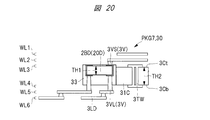
- FIG. 19 is a fragmentary cross-sectional view showing a relationship between a capacitor of a semiconductor device which is another modified example with respect to FIG. 18 and a core insulating layer in which a through-hole wiring is formed. It is principal part sectional drawing which shows the example of the embodiment which connects a via wiring to the capacitor incorporated in the wiring board.
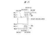
- FIG. 22 is a fragmentary cross-sectional view showing an example of an embodiment different from FIG. 21 in which a via wiring is connected to a capacitor built in a wiring board.
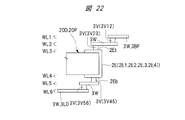
- FIG. 23 is a cross-sectional view of a principal part showing an example of an embodiment different from FIGS.
- FIG. 24 is a cross-sectional view of a principal part showing an example of an embodiment different from FIGS. 21 to 23 in which a via wiring is connected to a capacitor built in a wiring board.
- FIG. 26 is an enlarged cross-sectional view schematically showing a state in which an inspection is performed by short-circuiting an electrode of a DC cut capacitor in the electrical test process shown in FIG. 25.
- FIG. 25 is an enlarged cross-sectional view schematically showing a state in which an inspection is performed by short-circuiting an electrode of a DC cut capacitor in the electrical test process shown in FIG. 25.
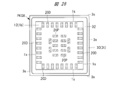
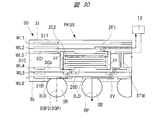
- FIG. 6 is a plan view showing an upper surface side of a semiconductor device which is a modified example with respect to FIG. 1.
- FIG. 29 is a bottom view of the semiconductor device shown in FIG. 28.
- FIG. 11 is an enlarged cross-sectional view schematically illustrating an example of a signal transmission path connected to a DC cut capacitor included in a semiconductor device which is a modification example of FIG. 10.
- FIG. 11 is an enlarged cross-sectional view schematically illustrating an example of a signal transmission path connected to a DC cut capacitor included in a semiconductor device which is another modification example of FIG. 10.
- FIG. 6 is a plan view showing a positional relationship between a plurality of capacitors and a semiconductor chip in a perspective plane viewed from the upper surface side of a wiring board included in a semiconductor device which is a study example for FIG. 5.
- FIG. 33 is an enlarged cross-sectional view schematically showing an example of a signal transmission path connected to the DC cut capacitor shown in FIG. 32.
- X consisting of A is an element other than A unless specifically stated otherwise and clearly not in context. It does not exclude things that contain.
- the component it means “X containing A as a main component”.
- silicon member is not limited to pure silicon, but includes a SiGe (silicon-germanium) alloy, other multi-component alloys containing silicon as a main component, and other additives. Needless to say, it is also included.
- gold plating, Cu layer, nickel / plating, etc. unless otherwise specified, not only pure materials but also members mainly composed of gold, Cu, nickel, etc. Shall be included.
- hatching or the like may be omitted even in a cross section when it becomes complicated or when it is clearly distinguished from a gap.
- the contour line of the background may be omitted even if the hole is planarly closed.
- hatching or a dot pattern may be added in order to clearly indicate that it is not a void or to clearly indicate the boundary of a region.
- FIG. 1 is an explanatory diagram illustrating a configuration example of an electronic device including the semiconductor device of this embodiment.
- FIG. 2 is an explanatory diagram illustrating a configuration example of a circuit included in the electronic device illustrated in FIG.
- the high-speed transmission path SGP2 illustrated in FIG. 2 is schematically illustrated by a bold line in order to explicitly indicate that the semiconductor device PKG1 and the semiconductor device PKG2 are electrically connected.
- the semiconductor device PKG1 and the semiconductor device PKG2 are electrically connected to each other via a signal transmission path SGP formed in the wiring board MB1.
- the electronic device EDV1 has a plurality of signal transmission paths SGP.
- the plurality of signal transmission paths SGP includes a low-speed transmission path SGP1 through which an electric signal is transmitted at the first transmission speed and an electric signal at a second transmission speed that is faster than the first transmission speed.
- a high-speed transmission path SGP2 through which is transmitted.
- the high-speed transmission path SGP2 is configured by a pair of differential signal transmission paths DSp and DSn through which a differential signal is transmitted.
- the semiconductor chip 11 included in the semiconductor device PKG1 is formed with, for example, a low-speed signal transmission electrode (electrode pad) TxL transmitted at the first transmission speed.
- the semiconductor chip 11 outputs a high-speed signal transmission electrode (electrode pad) Tx (specifically, a pair of differential signals) transmitted at a second transmission speed higher than the first transmission speed, for example.
- An electrode Txp and an electrode Txn) are formed.
- an electrode (electrode pad) RxL for receiving a low-speed signal transmitted at the first transmission speed is formed on the semiconductor chip 12 included in the semiconductor device PKG2.
- the semiconductor chip 12 receives, for example, a high-speed signal receiving electrode (electrode pad) Rx (specifically, a pair of differential signals) transmitted at a second transmission rate that is higher than the first transmission rate.
- An electrode Rxp and an electrode Rxn) are formed.
- an electrical signal is transmitted at a transmission speed less than 3 Gbps (Gigabit per second).
- an electric signal is transmitted at a transmission speed of about 3 Gbps to 100 Gbps.
- the capacitor 20D inserted in the high-speed transmission path SGP2 can cut the DC component included in the AC signal (in other words, block the DC component). Thereby, input / output of signals at high speed can be stabilized.
- the capacitor 20D inserted in series in the signal transmission path and cuts the DC component in the AC signal is referred to as a DC (Direct Current) cutting capacitor, an AC (Alternate Current) coupling capacitor, or , Referred to as a DC block capacitor (hereinafter referred to as a DC cut capacitor).
- the capacitor 20D which is a DC cut capacitor, is distinguished from a power supply capacitor 20P inserted in parallel in the power supply circuit, for example, as a capacitor 20P shown in FIG. 2 includes a reference potential supply path VSP for supplying a reference potential (first potential) VSS to the semiconductor chip 12, and a power supply potential supply for supplying a power supply potential (second potential) VDD to the semiconductor chip 12. It is inserted between the path VDP.
- the capacitor 20P can function as a bypass capacitor that bypasses noise (signal) included in the power supply potential supply path VDP to the reference potential supply path VSP side.
- the capacitor 20P reduces the influence of impedance components included in the power supply potential supply path VDP and the reference potential supply path VSP by reducing the loop (path distance) of the current flowing in the circuit formed in the semiconductor chip 12. It can function as a decoupling capacitor. Further, by connecting the capacitor 20P in the vicinity of the circuit that consumes the supplied power, it is possible to function as a battery that suppresses the phenomenon that the drive voltage drops instantaneously.
- bypass capacitor, decoupling capacitor, or power supply capacitor 20P used as a battery is all inserted in parallel in the power supply circuit.
- the capacitor 20D is inserted in series in the signal transmission path SGP. Therefore, as shown in FIG. 2, when the high-speed transmission path SGP2 is configured by the differential signal transmission paths DSp and DSn, the capacitor 20D is provided for the differential signal transmission path DSp and the differential signal transmission path DSn. Are inserted respectively.
- the state in which the capacitors are connected in series in the wiring path (signal transmission path or potential supply path) and the state in which the capacitors are connected in parallel can be defined as follows. That is, the capacitor has two electrodes, and can be defined by the connection destination of the wiring connected to the two electrodes.
- one electrode of the capacitor 20 ⁇ / b> D is connected to the electrode Rx of the semiconductor chip 12 through the first wiring.
- the other electrode of the capacitor 20D is connected to the land 3LH via a second wiring different from the first wiring.
- the land 3LH and the electrode Rx of the semiconductor chip 12 are electrically connected via the capacitor 20D. In this case, it can be said that the capacitor 20D is connected in series in a wiring path that electrically connects the electrode Rx of the semiconductor chip 12 and the land 3LH.
- one electrode of the capacitor 20P is connected to each of the electrode Vd and the land 3LVd of the semiconductor chip 12 through the first wiring.
- the other electrode of the capacitor 20P is connected to each of the electrode Vs and the land 3LVs of the semiconductor chip 12 via a second wiring different from the first wiring. In this case, it can be said that the capacitor 20P is connected in parallel between the wiring path for supplying the power supply potential to the semiconductor chip 12 and the wiring path for supplying the reference potential.
- the capacitor 20D can be mounted on the wiring board MB1 shown in FIG.
- the same number of capacitors 20D as the number of high-speed transmission paths is required.
- one (total two) capacitors 20D are required for each high-speed transmission path SGP2 of the differential pair. Become.
- the wiring constituting the high-speed transmission path SGP2 is formed on the inner layer of the wiring board MB1 shown in FIG. 1 (terminals on which the semiconductor devices PKG1 and PKG2 are mounted).
- the wiring layer is preferably formed on the wiring layer formed on the inner side of the wiring layer.
- an interlayer conductive layer that electrically connects stacked wiring layers such as vias and through holes (not shown). It will be necessary to route the road.
- Interlayer conductive paths such as vias and through holes cause impedance discontinuities in the high-speed transmission path SGP2. Therefore, from the viewpoint of improving the electrical characteristics of the high-speed transmission path SGP2, it is preferable to reduce the number of interlayer conductive paths included in the high-speed transmission path SGP2.
- the inventor of the present application studied a technique for mounting the capacitor 20D, which is a DC cut capacitor, in the semiconductor device PKG2 as shown in FIG.
- the layout of the wiring formed on the wiring board MB1 can be simplified.
- wiring board MB1 can be reduced in size.
- the capacitor 20D by mounting the capacitor 20D in the semiconductor device PKG2, the number of interlayer conductive paths inserted into the high-speed transmission path SGP2 included in the wiring board MB1 can be reduced. Thereby, the electrical characteristics of the high-speed transmission path SGP2 can be improved.
- a capacitor 20D is provided in the semiconductor device PKG2 having a circuit for reception. It is installed.
- one or more capacitors 20D may be inserted in the high-speed transmission path SGP2. Therefore, as a modification of FIG. 1, the capacitor 20D may be mounted on the semiconductor device PKG1 having a transmission circuit, and the capacitor 20D may not be mounted on the semiconductor device PKG2. As another modification to FIG. 1, the capacitor 20D can be mounted on both the semiconductor device PKG1 and the semiconductor device PKG2.
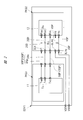
- FIG. 3 is a top view of a semiconductor device having a DC cut capacitor among the plurality of semiconductor devices shown in FIG.
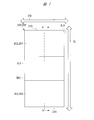
- FIG. 4 is a bottom view of the semiconductor device shown in FIG.
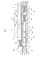
- FIG. 5 is a plan view showing the positional relationship between the plurality of capacitors and the semiconductor chip in the perspective plane seen from the upper surface side of the wiring board shown in FIG.
- FIG. 6 is an enlarged cross-sectional view along the line AA in FIG.
- FIGS. 3 to 6 the number of terminals is reduced for ease of viewing.
- the number of terminals (terminal 3BF, land 3LD, solder ball SB) is not limited to the mode shown in FIGS.
- the present invention can be applied to a semiconductor device having about 100 to 10,000 terminals such as terminals 3BF, lands 3LD, and solder balls SB.
- FIG. 5 the outlines of the plurality of capacitors built in the wiring board 30 are indicated by dotted lines in order to clearly show the planar positional relationship between the plurality of capacitors and the semiconductor chip.
- FIG. 5 is a top view, in order to make it easy to identify the capacitor 20D and the capacitor 20P among the plurality of capacitors, each of the plurality of capacitors 20P is hatched.
- FIG. 6 is a cross-sectional view, but hatching is omitted for each of the plurality of insulating layers 31 and the underfill resin for ease of viewing.
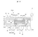
- the semiconductor device PKG2 of the present embodiment includes a wiring board 30, a semiconductor chip 12 (see FIG. 5) mounted on the wiring board 30, and a plurality of capacitors 20D and 20P built in the wiring board 30.
- the wiring substrate 30 includes an upper surface (surface, main surface, chip mounting surface) 3t on which the semiconductor chip 12 is mounted, and a lower surface (surface, main surface, mounting surface) 3b opposite to the upper surface 3t. , And a plurality of side surfaces 3s (see FIGS. 3 to 5) disposed between the upper surface 3t and the lower surface 3b, and form a rectangular outer shape in plan view as shown in FIGS.
- the planar size of the wiring board 30 is, for example, a square or rectangle having a side length of about 12 mm to 60 mm. Make it.
- the thickness (height) of the wiring board 30, that is, the distance from the upper surface 3t to the lower surface 3b shown in FIG. 6 is, for example, about 0.3 mm to 1.3 mm.
- the wiring board 30 is an interposer (relay board) for electrically connecting the semiconductor chip 12 mounted on the upper surface 3t side and the wiring board MB1 which is the mother board (mounting board) shown in FIG.
- the wiring substrate 30 has a plurality of wiring layers (six layers in the example shown in FIG. 6) WL1, WL2, WL3, WL4, WL5 that electrically connect the upper surface 3t side which is the chip mounting surface and the lower surface 3b side which is the mounting surface. , WL6.
- Each wiring layer has a conductor pattern such as a wiring that is a path for supplying an electric signal or electric power, and is covered with an insulating layer 31 that insulates a plurality of paths. Further, wiring layers adjacent in the thickness direction are electrically connected via interlayer conductive paths such as via wiring 3V and through-hole wiring 3TW.
- most of the wiring layer WL1 disposed on the uppermost surface 3t side is covered with the insulating layer 31T which is a solder resist film. Further, among the plurality of wiring layers, most of the wiring layer WL6 arranged on the lowermost surface 3b side is covered with the insulating layer 31B which is a solder resist film.
- the wiring board 30 is formed by laminating a plurality of wiring layers on the upper surface 3Ct and the lower surface 3Cb of the insulating layer (core material, core insulating layer) 31C made of a prepreg obtained by impregnating glass fiber with a resin, respectively, by a build-up method. To be formed. Further, the wiring layer WL3 on the upper surface 3Ct side and the wiring layer WL4 on the lower surface 3Cb side of the insulating layer 31C have a plurality of through holes (through-holes) provided so as to penetrate from one of the upper surface 3Ct and the lower surface 3Cb to the other. Are electrically connected via a plurality of through-hole wirings 3TW embedded in the holes).
- a plurality of terminals (bonding pads, bonding leads, chip connection terminals) 3BF electrically connected to the semiconductor chip 12 are formed on the upper surface 3t of the wiring board 30.
- the plurality of terminals 3BF and the plurality of lands 3LD are electrically connected through the wiring 3W, the via wiring 3V, and the through-hole wiring 3TW formed on the wiring board 30, respectively.
- the wiring board 30 is a wiring board in which a plurality of wiring layers are stacked on the upper surface 3Ct side and the lower surface 3Cb side of the insulating layer 31C, which is a core material.
- a so-called coreless substrate is used which does not have the insulating layer 31 ⁇ / b> C made of a hard material such as a prepreg material but is formed by sequentially laminating the insulating layer 31 and a conductor pattern such as the wiring 3 ⁇ / b> W. May be.
- the through-hole wiring 3TW is not formed, and each wiring layer is electrically connected via the via wiring 3V.
- FIG. 6 exemplarily shows a wiring board 30 having six wiring layers.
- a wiring board having seven or more wiring layers or five or less wiring layers is used. Also good.
- each of the wiring layers WL1, WL2, WL3, WL4, and WL6 is a conductor plane (pattern) 3PL formed so as to surround a conductor pattern such as the wiring 3W, the via wiring 3V, the through-hole wiring 3TW, and the land 3LD.
- the conductor plane 3PL is a conductor pattern formed in a region where a conductor pattern such as signal transmission wiring and terminals is not formed, and constitutes a part of a supply path for a reference potential or a power supply potential.
- the conductor plane 3PL is provided apart from a conductor pattern such as a conductor pattern such as the wiring 3W, the via wiring 3V, the through-hole wiring 3TW, and the land 3LD.
- the conductor plane 3PL When the conductor plane 3PL is formed in each wiring layer in this way, it is possible to suppress the spread of an electric field and a magnetic field spreading from the signal transmission path to the surroundings during signal transmission, and to suppress crosstalk noise from other signals. . Thereby, the noise tolerance of the signal transmission path can be improved.
- the conductor plane 3PL when a high-speed transmission path through which a signal is transmitted at a transmission speed of 3 Gbps or more is included, it is preferable to improve noise resistance by forming a conductor plane.
- the conductor plane 3PL may constitute a return path (return path) of the signal transmission path.
- solder ball SB solder material, external terminal, electrode, external electrode
- the solder ball SB is a conductive member that electrically connects a plurality of terminals (not shown) on the wiring board MB1 side and a plurality of lands 3LD when the semiconductor device PKG2 is mounted on the wiring board MB1 shown in FIG. It is.
- the solder ball SB is, for example, a Sn—Pb solder material containing lead (Pb), or a solder material made of so-called lead-free solder that does not substantially contain Pb.
- lead-free solder examples include tin (Sn) only, tin-bismuth (Sn-Bi), tin-copper-silver (Sn-Cu-Ag), tin-copper (Sn-Cu), and the like.
- the lead-free solder means a lead (Pb) content of 0.1 wt% or less, and this content is defined as a standard of the RoHS (Restriction of az Hazardous Substances) directive.
- the plurality of solder balls SB are arranged in a matrix (array or matrix).
- a plurality of lands 3LD (see FIG. 6) to which a plurality of solder balls SB are joined are also arranged in a matrix (matrix).
- a semiconductor device in which a plurality of external terminals (solder balls SB and lands 3LD) are arranged in a matrix on the mounting surface side of the wiring board 30 is referred to as an area array type semiconductor device. Since the area array type semiconductor device can effectively utilize the mounting surface (lower surface 3b) side of the wiring substrate 30 as an external terminal arrangement space, the mounting area of the semiconductor device increases even if the number of external terminals increases. It is preferable at the point which can suppress. That is, a semiconductor device in which the number of external terminals increases with higher functionality and higher integration can be mounted in a space-saving manner.
- the semiconductor device PKG2 includes a semiconductor chip 12 mounted on the wiring board 30.
- each of the semiconductor chips 12 includes a front surface (main surface, upper surface) 1t, a back surface (main surface, lower surface) 1b opposite to the front surface 1t, and between the front surface 1t and the back surface 1b.
- it has a rectangular outer shape that has a side surface 1s and has a smaller plane area than the wiring board 30 in plan view.
- the semiconductor chip 12 is mounted on the upper surface 3 t of the wiring substrate 30 with each of the four side surfaces 1 s extending along the four side surfaces 3 s of the wiring substrate 30.
- a plurality of pads (electrode pad bonding pads) 1PD are formed on the surface 1t side of the semiconductor chip 12.
- the plurality of pads 1PD are exposed from the passivation film that protects the surface 1t of the semiconductor chip 12 on the surface 1t of the semiconductor chip 12.
- a plurality of pads 1PD are arranged in a matrix (matrix or array) on the surface 1t of the semiconductor chip 12.
- the semiconductor chip 12 is mounted on the wiring board 30 with the surface 1t being arranged to face the upper surface 3t of the wiring board 30.
- a mounting method is called a face-down mounting method or a flip-chip connection method.
- the main surface of the semiconductor chip 12 (specifically, a semiconductor element formation region provided on an element formation surface of a semiconductor substrate that is a base material of the semiconductor chip 12) includes a plurality of semiconductor elements (circuits). Element) is formed.
- the plurality of pads 1PD are connected to the plurality of pads 1PD via wiring (not shown) formed in a wiring layer disposed inside the semiconductor chip 12 (specifically, between the surface 1t and a semiconductor element formation region (not shown)). Each is electrically connected to the semiconductor element.
- the semiconductor chip 12 (specifically, the base material of the semiconductor chip 12) is made of, for example, silicon (Si).
- an insulating film is formed on the surface 1t to cover the base material and wiring of the semiconductor chip 12, and a part of each of the plurality of pads 1PD is formed from the insulating film in an opening formed in the insulating film. Exposed.
- each of the plurality of pads 1PD is made of metal, and in the present embodiment, for example, aluminum (Al).
- the plurality of pads 1PD are connected to the protruding electrodes 1BP, respectively, and the plurality of pads 1PD of the semiconductor chip 12 and the plurality of terminals 3BF of the wiring board 30 are connected to the plurality of protruding electrodes 1BP.
- the protruding electrode (bump electrode) 1BP is a metal member (conductive member) formed so as to protrude on the surface 1t of the semiconductor chip 12.
- the protruding electrode 1BP is a so-called solder bump in which a solder material is laminated on the pad 1PD via a base metal film (under bump metal).
- the base metal film is, for example, a laminated film in which titanium (Ti), copper (Cu), and nickel (Ni) are laminated from the connection surface side with the pad 1PD (when a gold (Au) film is further formed on the nickel film) Can also be exemplified.
- solder material constituting the solder bump lead-containing solder material or lead-free solder can be used as in the case of the solder ball SB.
- solder bumps are integrated to form the protruding electrode 1BP.
- a pillar bump columnar electrode in which a solder film is formed on the tip surface of a conductor column made of copper (Cu) or nickel (Ni) may be used as the protruding electrode 1BP.
- the semiconductor chip 12 includes a circuit for inputting / outputting a plurality of signals having different transmission speeds.
- the semiconductor chip 12 includes a first circuit that inputs and outputs a first signal at a first transmission speed, and a second signal at a second transmission speed that is faster than the first transmission speed. And a second circuit for inputting and outputting.
- the second signal for example, a differential signal is transmitted at a transmission rate of about 3 Gbps (Gigabit per second) to 100 Gbps.
- a transmission path through which the second signal is transmitted is described as a high-speed transmission path.
- the first circuit is supplied with a first drive voltage for driving the first circuit in addition to the first signal.
- the second circuit is supplied with a second drive voltage for driving the second circuit, in addition to the second signal.
- an underfill resin (insulating resin) 32 is disposed between the semiconductor chip 12 and the wiring board 30.
- the underfill resin 32 is disposed so as to block the space between the surface 1t of the semiconductor chip 12 and the upper surface 3t of the wiring board 30.
- the underfill resin 32 is made of an insulating (non-conductive) material (for example, a resin material), and seals an electrical connection portion between the semiconductor chip 12 and the wiring board 30 (joint portions of the plurality of protruding electrodes 1BP). To be arranged.
- the stress generated in the electrical connection portion between the semiconductor chip 12 and the wiring board 30 can be relaxed.
- the stress generated at the joints between the plurality of pads 1PD and the plurality of protruding electrodes 1BP of the semiconductor chip 12 can be relaxed.
- the main surface of the semiconductor chip 12 on which the semiconductor element (circuit element) is formed can be protected.
- the semiconductor device PKG2 includes a plurality of capacitors 20D and 20P mounted on the wiring board 30.
- the semiconductor device PKG2 includes a plurality of capacitors 20D and 20P built in the wiring board 30.
- the above-mentioned “built in the wiring board 30” is defined as follows.
- the entire capacitor 20D and the entire capacitor 20P are arranged between the upper surface 3t and the lower surface 3b of the wiring board 30.
- the capacitor 20 ⁇ / b> P and the capacitor 20 ⁇ / b> D are built in the wiring board 30.
- the semiconductor chip 12 shown in FIG. 6 does not exist between the upper surface 3 t and the lower surface 3 b of the wiring substrate 30. In this case, the semiconductor chip 12 is not built in the wiring board 30.
- an electronic component such as a capacitor is disposed between the upper surface 3 t and the lower surface 3 b of the wiring board 30, and the other part is above the upper surface 3 t of the wiring board 30.
- positioned other than between the lower surfaces 3b so that it may protrude below the lower surface 3b can be considered.
- the electronic component is handled as a state where it is not built in the wiring board 30.
- At least one of the upper surface 3t and the lower surface 3b of the wiring board 30 exposes electrodes of electronic components such as capacitors, and a portion (main part) other than the exposed electrodes includes the upper surface 3t and The case where it arrange
- the electronic component is handled as being incorporated in the wiring board 30.
- the main part (main body part) excluding the electrodes and terminals of the electronic component is disposed between the upper surface 3t and the lower surface 3b of the wiring substrate 30, the electronic component is built in the wiring substrate 30. Treat as a state.
- the incorporation of the capacitor 20D in the wiring board 30 and the incorporation of the capacitor 20P in the wiring board 30 have different effects. Details of the effects will be described later.
- a heat radiating plate (heat spreader, member) 40 is attached to the back surface 1 b of the semiconductor chip 12.
- the heat radiating plate 40 is, for example, a metal plate having a higher thermal conductivity than the wiring board 30 and has a function of discharging heat generated in the semiconductor chip 12 to the outside.
- the heat radiating plate 40 is attached to the back surface 1 b of the semiconductor chip 12 via an adhesive (heat radiating resin) 41.
- the adhesive 41 has a higher thermal conductivity than the underfill resin 32 by containing, for example, a large number of metal particles and filler (for example, alumina).
- a support frame (stiffener ring) 42 that supports the heat sink 40 is fixed around the semiconductor chip 12.
- the heat radiating plate 40 is bonded and fixed to the back surface 1 b of the semiconductor chip 12 and the support frame 42. Fixing the metallic support frame 42 around the semiconductor chip 12 can suppress warping deformation of the wiring board 30, which is preferable from the viewpoint of improving mounting reliability.
- the heat radiation plate 40 can be enlarged by bonding and fixing the heat radiation plate 40 to the support frame 42 provided so as to surround the periphery of the semiconductor chip 12. That is, it is preferable that the heat radiating plate 40 is bonded and fixed to the support frame 42 from the viewpoint of improving the heat radiating performance by securing a large surface area of the heat radiating plate 40 and stably fixing it on the semiconductor chip 12.
- the embodiment in which the heat sink 40 is attached to the back surface 1b of the semiconductor chip 12 has been described as an example. However, as a modification, the heat sink 40 is not attached and the semiconductor chip 12 is not attached. It is good also as an embodiment which the back surface 1b exposed.
- FIG. 7 is a plan view showing one of the plurality of capacitors shown in FIG.
- FIG. 8 is a sectional view taken along line AA in FIG.
- FIG. 32 is a plan view showing the positional relationship between the plurality of capacitors and the semiconductor chip in a perspective plane viewed from the upper surface side of the wiring board included in the semiconductor device which is the examination example with respect to FIG.
- FIG. 9 is an enlarged cross-sectional view of a semiconductor device which is a modification to FIG.
- FIGS. 7 and 8 show a structure example of one capacitor as a representative example of the capacitor 20D and the capacitor 20P.
- the extending direction DL of the capacitors 20D and 20P and the width direction DW are schematically shown with arrows.
- FIG. 32 is a plan view similar to FIG. 5, but hatching is given to each of the plurality of capacitors 20 ⁇ / b> P in order to facilitate identification of the capacitor 20 ⁇ / b> D and the capacitor 20 ⁇ / b> P among the plurality of capacitors.
- a plurality of capacitors 20D and 20P are mounted on the wiring board 30 of the present embodiment.
- the plurality of capacitors 20D and 20P include the capacitor 20D that is a DC cut capacitor and the capacitor 20P for a power supply circuit that is used as a bypass capacitor, a decoupling capacitor, or a battery as described above.
- some of the capacitors 20 ⁇ / b> D and 20 ⁇ / b> P are shown with reference numerals.
- a plurality of capacitors (capacitors with hatching) arranged at positions overlapping the semiconductor chip 12 are all capacitors 20P, and each of the plurality of capacitors 20D is connected to a plurality of capacitors 20P.
- each of the plurality of capacitors 20 ⁇ / b> D is disposed at a position that does not overlap the semiconductor chip 12. In the example illustrated in FIG. 5, the plurality of capacitors 20 ⁇ / b> D are disposed outside the support frame 42.
- each of the capacitors (chip capacitors) 20D and 20P has a quadrangular shape in plan view.
- the capacitors 20D and 20P include two long sides (long side surfaces) 2LS extending along the extending direction (longitudinal direction) DL and two short sides extending along the width direction DW orthogonal to the extending direction DL.
- Capacitors 20D and 20P have electrode 2E1 and electrode 2E2 (or electrode 2E3 and electrode 2E4) arranged at ends opposite to each other in extending direction DL (in other words, in the extending direction of long side 2LS). Have.
- the capacitors 20D and 20P have a main body 2BD sandwiched between the electrodes 2E1 and 2E3 and the electrodes 2E2 and 2E4.
- the main body 2BD has a plurality of conductor plates 20CL stacked via an insulating layer (dielectric layer) 20IL, and each of the plurality of conductor plates 20CL includes electrodes 2E1, 2E3. And one of the electrodes 2E2, 2E4.
- the electrodes 2E1 and 2E3 and the electrodes 2E2 and 2E4 function as external electrode terminals for taking out the capacitance formed between the plurality of conductive plates arranged opposite to each other.
- an example of the structure of the capacitors 20D and 20P has been described. However, there are various modifications to the structures of the capacitors 20D and 20P.
- the capacitors 20D and 20P shown in FIG. 7 exemplarily show a capacitor structure in which electrodes are arranged so as to cover each of the short sides 2SS.
- an electrode may be arranged so as to cover the long side 2LS. That is, the position of the capacitor electrode may be either the short side 2SS or the long side 2LS.
- each of the plurality of capacitors 20P for the power supply circuit is connected in parallel in the power supply circuit so as to connect the first potential and the second potential of the power supply circuit.
- the plurality of pads 1PD included in the semiconductor chip 12 shown in FIG. 6 includes an electrode (electrode pad) Vs (see FIG. 2) to which the reference potential VSS (see FIG. 2) is supplied and a power supply potential VDD (see FIG. 2). ) Is supplied (electrode pad) Vd (see FIG. 2).
- 6 includes a land 3LVs (see FIG. 2) to which the reference potential VSS is supplied and a land 3LVd (see FIG.
- one electrode of the capacitor 20P is connected to the reference potential supply path VSP side connecting the electrode Vs and the land 3LVs, and the other electrode of the capacitor 20P is connected to the electrode Vd and the land 3LVd. Connected to the power supply potential supply path VDP side to be connected.
- each of the plurality of capacitors 20P is arranged at a position overlapping the semiconductor chip 12 in plan view.
- each of the plurality of capacitors 20 ⁇ / b> P is built in the wiring board 30. For this reason, each of the plurality of capacitors 20 ⁇ / b> P can be arranged at a position overlapping the semiconductor chip 12.
- each of the plurality of capacitors 20P for the power supply circuit is arranged at a position overlapping the semiconductor chip 12, compared to the case where the capacitor 20P is arranged around the semiconductor chip 12.
- the transmission distance between the capacitor 20P and the semiconductor chip 12 can be shortened.
- the electrical characteristics of the power supply circuit can be improved by shortening the transmission distance between the capacitor 20P for the power supply circuit and the semiconductor chip 12.
- the capacitor 20P when the capacitor 20P is used as a bypass capacitor, the noise flowing in the circuit that consumes power can be reduced by inserting the capacitor 20P near the circuit that consumes power. Further, for example, when the capacitor 20P is used as a decoupling capacitor, the loop of the current flowing through the circuit formed in the semiconductor chip 12 (path distance) can be reduced by reducing the distance between the capacitor 20P and the semiconductor chip 12. Can do. As a result, the influence of impedance components included in the power supply potential supply path VDP and the reference potential supply path VSP shown in FIG. 2 can be reduced. In addition, for example, when the capacitor 20P is used as a battery, it is easy to suppress the phenomenon that the drive voltage drops instantaneously by reducing the distance between the circuit that consumes power and the capacitor 20P.
- each of the plurality of DC cut capacitors 20D is inserted into the high-speed transmission path SGP2 shown in FIG. 2 in series connection.
- the plurality of pads 1PD included in the semiconductor chip 12 illustrated in FIG. 6 include electrodes (electrode pads) RxL (see FIG. 2) for low-speed signals that are transmitted at a relatively low first transmission speed.
- . 6 includes electrodes (electrode pads) Rxp, Rxn for high-speed signals transmitted at a second transmission speed higher than the first transmission speed (see FIG. 2). Reference).
- the plurality of lands 3LD included in the wiring board 30 illustrated in FIG. 6 include low-speed signal lands 3LL (see FIG.
- each of the electrodes Rxp and Rxn is electrically connected to the land 3LH via the capacitor 20D.
- one electrode of the capacitor 20D is connected to the electrode Rxp or the electrode Rxp side of the semiconductor chip 12 in the high-speed transmission path SGP2, and the other electrode of the capacitor 20D is connected to the land 3LH side of the high-speed transmission path SGP2. Connected to. More specifically, as shown in FIG.
- one electrode of the capacitor 20 ⁇ / b> D is electrically connected to the pad 1 ⁇ / b> PD of the semiconductor chip 12 through the wiring 3 ⁇ / b> W of the wiring board 30.
- the other electrode of the capacitor 20D is connected to the land 3LD through another wiring 3W of the wiring board 30.
- the capacitor 20D is connected to the land 3LD and the semiconductor. It can be said that they are connected in series in the wiring path connecting the chip 12.
- the electrode RxL and the land 3LL constituting the low-speed transmission path SGP1 shown in FIG. 2 are electrically connected without passing through a capacitor.
- each of the capacitors 20P for the power supply circuit included in the semiconductor device PKG2 of the present embodiment is disposed at a position overlapping the semiconductor chip 12. Further, each of the plurality of DC cut capacitors 20D included in the semiconductor device PKG2 is disposed between the plurality of capacitors 20P and the peripheral portion of the wiring substrate 30 (each side constituting the periphery of the upper surface 3t) in plan view. Has been.
- each of the plurality of capacitors 20D is inserted in series in the middle of the signal transmission path for high-speed signals (high-speed transmission path SGP2 shown in FIG. 2). Therefore, the wiring board 30 includes a wiring path that electrically connects each of the plurality of capacitors 20 ⁇ / b> D and the semiconductor chip 12. Therefore, when increasing the density of the high-speed transmission path, it is necessary to arrange these wiring paths at a high density.
- each of the plurality of capacitors 20P is not built in the wiring board 30 but arranged around the semiconductor chip 12 as in the semiconductor device PKGh1 which is a modified example shown in FIG.
- the semiconductor device PKGh1 is different from the semiconductor device PKG2 shown in FIG. 5 in that a plurality of capacitors 20P are mounted on the upper surface 3t of the wiring board 30 and arranged between the semiconductor chip 12 and the plurality of capacitors 20D. Is different. Further, the semiconductor device PKGh1 is different from the semiconductor device PKG2 shown in FIG. 5 in that each of the plurality of capacitors 20D is mounted on the upper surface 3t of the wiring board 30.
- a capacitor for a power supply circuit is provided between the semiconductor chip 12 and the capacitor 20D.
- 20P electrodes 2E3 and 2E4 are arranged. For this reason, it is necessary to form a terminal for supplying a potential to the capacitor 20P in a position overlapping the electrodes 2E3 and 2E4 of the capacitor 20P in the uppermost wiring layer of the wiring board 30.
- a terminal for a power supply circuit is formed between the semiconductor chip 12 and the capacitor 20D, the high-speed transmission path is hindered.
- the wiring for the high-speed transmission path is arranged directly under the terminal for the power supply circuit, the influence on the return path of the high-speed transmission path becomes large.
- the wiring is formed by selecting a region where the capacitor 20P is not disposed. There is a need. This makes it difficult to arrange a large number of high-speed transmission paths at high density.
- the plurality of capacitors 20 ⁇ / b> P are built in the wiring board 30, and are arranged at positions overlapping the semiconductor chip 12.
- each of the plurality of capacitors 20D is arranged between the plurality of capacitors 20P and the peripheral portion of the wiring substrate 30 (each side constituting the periphery of the upper surface 3t) in plan view. Yes.
- each of the plurality of capacitors 20D is disposed around a region where the plurality of capacitors 20D are disposed in plan view.
- the capacitor 20D is not arranged in the wiring path connecting the capacitor 20D and the semiconductor chip 12. For this reason, the layout of the high-speed transmission path connected to the capacitor 20D is not hindered by the terminals connected to the capacitor 20P and can be increased in density.
- the capacitor 20P since the capacitor 20P is built in the wiring board 30, it is not necessary to provide a space for mounting the capacitor 20P around the semiconductor chip 12 as in the semiconductor device PKGh1 shown in FIG. . For this reason, since the distance between the semiconductor chip 12 and the capacitor 20D can be reduced, the inductance and resistance of the wiring path connecting the capacitor 20D and the semiconductor chip 12 can be reduced.
- each of the plurality of capacitors 20 ⁇ / b> D and the peripheral edge of the wiring board 30 is smaller than the distance between each of the plurality of capacitors 20 ⁇ / b> D and the semiconductor chip 12 in plan view.
- each of the plurality of capacitors 20 ⁇ / b> D is arranged close to the peripheral edge side of the upper surface 3 t of the wiring board 30.
- each of the plurality of capacitors 20 ⁇ / b> D is arranged close to the peripheral edge side of the upper surface 3 t of the wiring substrate 30, the arrangement density of the high-speed transmission paths can be improved in the region near the semiconductor chip 12. .
- each of the plurality of effects described in this section can be obtained regardless of whether or not each of the plurality of capacitors 20D is built in the wiring board 30. Therefore, as in the semiconductor device PKG3 shown in FIG. 9 which is a modification to FIG. 6, each of the plurality of capacitors 20P is built in the wiring board 30, and a part or all of the plurality of capacitors 20D are part of the wiring board. 30 may be mounted on the upper surface 3t.
- FIG. 10 is an enlarged cross-sectional view schematically showing an example of a signal transmission path connected to the DC cut capacitor shown in FIG.
- FIG. 11 is an enlarged plan view showing the periphery of a region in which a DC cut capacitor of a semiconductor device, which is a modification of FIG. 5, is built.
- FIG. 12 is an enlarged cross-sectional view of the semiconductor device shown in FIG. FIG.
- FIG. 13 is an enlarged plan view showing an enlargement of the periphery of a region in which a DC cut capacitor of a semiconductor device, which is another modification of FIG. 5, is built.
- FIG. 14 is an enlarged cross-sectional view of the semiconductor device shown in FIG.
- FIG. 33 is an enlarged cross-sectional view schematically showing an example of a signal transmission path connected to the DC cut capacitor shown in FIG.
- FIG. 10 in order to clearly indicate the signal transmission path and the return path via the capacitor 20D, the high-speed transmission path SGP2 uses a two-dot chain line, and the return path RP uses a dotted line. This is shown schematically.
- FIG. 11 and FIG. 13 an example of a wiring path that connects the capacitor 20D and the test terminal 3TP is indicated by a dotted line.
- 10, 12, 14, and 33 are cross-sectional views, but hatching is omitted except for components mounted on the wiring board for easy understanding of the signal transmission path.
- the capacitor 20 ⁇ / b> D included in the semiconductor device PKG ⁇ b> 2 of the present embodiment is built in the wiring board 30.
- the capacitor 20 ⁇ / b> D included in the semiconductor device PKGh ⁇ b> 1 shown in FIG. 33 is not built in the wiring board 30 but is mounted on the upper surface 3 t of the wiring board 30.
- the semiconductor device PKG2 shown in FIG. 10 and the semiconductor device PKGh1 shown in FIG. 33 when the capacitor 20D is built in the wiring board 30, it is compared with the case where the capacitor 20D is mounted on the wiring board 30.
- the high-speed transmission path SGP2 and the return path RP change greatly.
- the high-speed transmission path SGP2 of the semiconductor device PKG2 has fewer impedance discontinuities than the high-speed transmission path SGP2 of the semiconductor device PKGh1.
- the impedance discontinuity point is a place where the impedance value changes rapidly in a part of the wiring path. For this reason, for example, in the portion of the interlayer conductive path such as the via wiring 3V and the through-hole wiring 3TW, the wiring structure is changed, so that it is likely to be an impedance discontinuity point.
- the number of via wirings 3V and the number of through-hole wirings 3TW included in the high-speed transmission path SGP2 are small compared to the case of the semiconductor device PKGh1 shown in FIG. For this reason, impedance discontinuity points included in the high-speed transmission path SGP2 can be reduced, and transmission characteristics can be improved.
- the capacitor 20D is arranged between the upper surface 3Ct and the lower surface 3Cb of the insulating layer 31C as the core material. For this reason, the high-speed transmission path SGP2 connected to the capacitor 20D is electrically separated from the through-hole wiring 3TW. In other words, the high-speed transmission path SGP2 connected to the capacitor 20D is electrically connected to the semiconductor chip 12 without passing through the through-hole wiring 3TW.
- the impedance value is likely to change greatly in the through-hole wiring 3TW and the capacitor 20D, so that the influence on the transmission characteristics is particularly large compared to the via wiring 3V. Therefore, as shown in FIG. 10, by embedding the capacitor 20D in the insulating layer 31C provided with the through-hole wiring 3TW, one through-hole wiring 3TW can be omitted, so that the high-speed transmission path SGP2 Transmission characteristics can be particularly improved.
- the electrical test of the circuit formed in the semiconductor device PKG2 may include a DC test in which a direct current is passed through the circuit for inspection.
- the DC test includes, for example, a continuity test for confirming the electrical connection state of the circuit.
- one electrode 2E1 (see FIG. 7) and the other electrode 2E2 of the capacitor 20D are used in order to pass a direct current.
- the electrode 2E1 (see FIG. 7) and the electrode 2E2 (see FIG. 7) of the capacitor 20D are provided on the wiring board 30. It is embedded between the upper surface 3t and the lower surface 3b and may not be exposed.
- the electrode 2E1 and the electrode 2E2 of the capacitor 20D are not exposed to the outside of the wiring board 30, another method for bypassing the electrodes of the capacitor 20D is necessary when performing the DC test. Therefore, in the present embodiment, each of the test terminal 3TP connected to one electrode 2E1 of the capacitor 20D and the test terminal 3TP connected to the other electrode 2E2 can be exposed from the wiring board 30. Provided. Thereby, when performing a DC test, a direct current can be sent through the high-speed transmission path SGP2 by electrically connecting the two terminals 3TP.
- the wiring board 30 of the present embodiment is arranged on the upper surface 3t side and is electrically connected to a plurality of pads 1PD of the semiconductor chip 12 (chip connection terminals) 3BF. And lands 3LD which are a plurality of external terminals arranged on the lower surface 3b side.
- the wiring board 30 includes a test terminal 3TP1 and a terminal 3TP2 that are connected to the capacitor 20D and exposed from the wiring board 30.
- one electrode 2E1 of the capacitor 20D is connected to a chip connecting terminal 3BF (see FIG. 6) and a test terminal 3TP1.
- the other electrode 2E2 of the capacitor 20D is connected to the land 3LD which is an external terminal and the other terminal 3TP2 for testing.
- each of the plurality of test terminals 3TP is exposed from the uppermost insulating layer 31T on the upper surface 3t of the wiring board 30.
- the test terminal 3TP may be formed on the lower surface 3b side and exposed from the lowermost insulating layer 31B on the lower surface 3b of the wiring board 30.
- the state where “the capacitor 20D is built in the wiring board 30” includes the following cases. That is, the electrodes 2E1 and 2E2 of the capacitor 20D are exposed on at least one of the upper surface 3t and the lower surface 3b of the wiring board 30, and portions (main parts) other than the exposed electrodes are the upper surface 3t and the lower surface It is a case where it arrange
- a portion exposed from the wiring board 30 in each of the electrode 2E1 and the electrode 2E2 of the capacitor 20D may be used instead of the above-described test terminal 3TP. That is, when performing the DC test, a portion exposed from the wiring board 30 in each of the electrode 2E1 and the electrode 2E2 of the capacitor 20D may be short-circuited.
- the wiring path connected to the terminal 3TP is a signal transmission path.
- the wiring path distance from the electrode 2E1 of the capacitor 20D to the terminal 3TP1 of the wiring board 30 and the wiring path distance from the electrode 2E2 of the capacitor 20D to the terminal 3TP2 of the wiring board 30 are the capacitor 20D. It is 1/4 or less of the wavelength of the electric signal supplied to. Thereby, it can suppress that signal strength falls by the influence of the wiring path
- each of the plurality of test terminals 3TP is arranged at a position overlapping the capacitor 20D in plan view. It is preferable.
- each of the plurality of test terminals 3TP may be arranged at a position not overlapping the capacitor 20D.
- the capacitor 20D is arranged at a position overlapping the heat sink 40 and the support frame 42 that supports the heat sink 40. There may be.
- each of the plurality of test terminals 3TP is arranged between the heat sink 40 and the peripheral edge of the wiring board 30 in plan view. It is preferable that In the example shown in FIGS. 11 and 12, the test terminal 3TP is disposed between the capacitor 20D and the peripheral edge of the wiring board 30.
- the heat sink 40 is covered to the vicinity of the peripheral edge of the upper surface 3t of the wiring board 30.
- the test terminal 3TP it is difficult to arrange the test terminal 3TP on the upper surface 3t side.
- the DC test can be performed with the heat sink 40 attached. it can.
- Each of the plurality of effects described in this section can be obtained with or without the plurality of capacitors 20P shown in FIG. Therefore, even in the case of a semiconductor device (not shown) in which the plurality of capacitors 20P shown in FIG. 5 are mounted, the case where each of the plurality of capacitors 20D is built in the wiring board 30 is described in this section. An effect is obtained.
- FIG. 15 is an enlarged plan view of a wiring layer in which a capacitor is embedded among the plurality of wiring layers shown in FIG.
- FIG. 16 is an enlarged plan view of the upper wiring layer of the wiring layer shown in FIG.
- FIG. 17 is an enlarged plan view of the upper wiring layer of the wiring layer shown in FIG.
- the wiring 3W and the like are provided.
- a conductor plane 3PL is arranged in a region that is not formed.
- conductor planes 3PL are formed in the wiring layers WL1 (see FIG. 17) to the wiring layers WL3 (see FIG. 17), respectively.
- an opening 3K3 is formed in a part of the conductor plane 3PL, an opening 3K3 is formed, and a capacitor 20D is embedded inside the opening 3K3.
- the conductor plane 3PL is arranged at a position overlapping the electrodes 2E1 and 2E2 of the capacitor 20D, and most of the capacitor 20D covers the conductor plane 3PL. It has been found that there is a concern that the transmission characteristics of the high-speed transmission path may deteriorate. That is, it has been found that capacitive coupling occurs between the conductor plane 3PL and the electrodes 2E1 and 2E2, and parasitic capacitance is added in the transmission path.
- the electrode 2E1 and the electrode 2E2 of the capacitor 20D are considered to have a wiring width (minimum width dimension) such as a lead wiring (for example, the wiring 3W shown in FIG. 16) in consideration of the freedom of the connection position. ) Is difficult.
- the “minimum width dimension” of the electrode 2E1 and the electrode 2E2 referred to here is, for example, the shortest length in the width direction DW shown in FIG.
- the value of the parasitic capacitance increases in proportion to the area of the portion that overlaps mainly in the thickness direction.
- parasitic capacitance is added to the electrode 2E1 and the electrode 2E2 constituting the high-speed transmission path, the impedance in the high-speed transmission path apparently decreases. That is, an impedance discontinuity occurs by adding a low impedance part to a part of the high-speed transmission path.
- the wiring layout is designed so that the impedance component in the transmission path approaches a predetermined value (for example, 50 ohms for a single wire, 100 ohms for a differential, or 85 ohms for a differential). Therefore, it is possible to suppress deterioration of characteristics such as signal reflection. Therefore, from the viewpoint of improving signal transmission quality, it is preferable to reduce the parasitic capacitance generated between the electrodes 2E1 and 2E2 and the conductor plane 3PL as much as possible to achieve impedance matching.
- a predetermined value for example, 50 ohms for a single wire, 100 ohms for a differential, or 85 ohms for a differential. Therefore, it is possible to suppress deterioration of characteristics such as signal reflection. Therefore, from the viewpoint of improving signal transmission quality, it is preferable to reduce the parasitic capacitance generated between the electrodes 2E1 and 2E2 and the conductor plane 3PL as much as possible to achieve impedance matching.
- the present inventor has found a method for suppressing the occurrence of impedance discontinuity in the electrode 2E1 and the electrode 2E2 for mounting the capacitor 20D when the capacitor 20D is mounted in a semiconductor device. That is, as shown in FIG. 16, the conductor plane 3PL of the wiring layer WL2 adjacent to the wiring layer WL3 on which the electrodes 2E1 and 2E2 of the capacitor 20D are arranged is formed in a region overlapping each of the electrode 2E1 and the electrode 2E2. It has an opening 3K2.
- the relationship between the electrodes 2E1 and 2E2 shown in FIG. 16 and the conductor plane 3PL can also be expressed as follows. That is, the conductor plane 3PL included in the wiring layer WL2 has an opening that overlaps each of the electrode 2E1 and the electrode 2E2.
- the insulating layer 31 covering the wiring layer WL3 (see FIG. 15) further inside than the wiring layer WL2 is exposed. .
- the value of the parasitic capacitance caused by capacitive coupling increases in proportion to the area of the portion where the conductor plane 3PL and the electrode 2E1 or 2E2 overlap in the thickness direction. Therefore, as shown in FIG. 16, it is particularly preferable that the electrode 2E1 and the electrode 2E2 as a whole do not overlap the conductor plane 3PL in the thickness direction.
- the outline of the electrode 2E1 and the outline of the electrode 2E2 are located inside the opening end portion (periphery portion of the opened region) of the opening 3K2 in plan view. It is preferable.
- the value of the parasitic capacitance can be reduced. For example, if 90% or more of the planar areas of the electrode 2E1 and the electrode 2E2 do not overlap with the conductor plane 3PL, the value of the parasitic capacitance can be reduced.
- the shape of the opening 3K2 shown in FIG. 16 preferably corresponds to the shape and position of the electrode 2E1 and the electrode 2E2 in the wiring layer WL3 (see FIG. 15). As shown in FIG. 16, if the opening 3K2 is formed so as to include the entire region overlapping with the electrode 2E1 and the electrode 2E2, the value of the parasitic capacitance is large even if the area of the opening 3K2 becomes larger than that. Does not reduce.
- the conductor plane 3PL may be used as a reference path (return path) of a high-speed transmission path.
- the conductor plane 3PL may be used as a reference path (return path) of a high-speed transmission path.
- the distance between the reference path and the high-speed transmission path it is preferable to keep the distance between the reference path and the high-speed transmission path constant. Therefore, it is preferable that the area of the opening 3K2 is not extremely large.
- the outline of the opening end of the opening 3K2 is preferably along the outline of the electrodes 2E1 and 2E2 in the wiring layer WL3 (see FIG. 15).
- the electrode 2E1 and the electrode 2E2 that constitute a part of the high-speed transmission path are formed in the wiring layer WL3.
- the conductor plane 3PL formed in the wiring layer WL2 adjacent to the wiring layer WL3 in the thickness direction regions overlapping the electrodes 2E1 and 2E2 are opened.
- the semiconductor device PKG2 see FIG. 5 of the present embodiment can improve the noise resistance of the high-speed transmission path, the electrical characteristics, reliability, and reliability can be improved.
- the conductor plane 3PL included in the wiring layer WL1 stacked on the wiring layer WL2 (see FIG. 16) is in a region overlapping each of the electrode 2E1 and the electrode 2E2. It has the opening 3K1 formed. Inside the opening 3K1, a test terminal 3TP1 and a terminal 3TP2 are arranged.
- the relationship between the electrodes 2E1 and 2E2 shown in FIG. 17 and the conductor plane 3PL can also be expressed as follows. That is, the conductor plane 3PL included in the wiring layer WL1 has an opening in the region overlapping with each of the electrode 2E1 and the electrode 2E2.
- the parasitic capacitance added to the electrode 2E1 and the electrode 2E2 it is capacitive coupling with the conductor plane 3PL of the wiring layer WL2 closest to the wiring layer WL3. Therefore, as described above, by forming the opening 3K2 as described above in the conductor plane 3PL of the wiring layer WL2, the value of the parasitic capacitance can be greatly reduced. Therefore, regardless of the wiring structure of the wiring layer WL1, the noise resistance of the high-speed transmission path can be improved by providing the opening 3K2 shown in FIG.
- capacitive coupling with the conductor plane 3PL formed in the wiring layer WL1 having the smallest separation distance from the wiring layer WL3 next to the wiring layer WL2 Is preferably taken into account.
- the thickness of each wiring layer tends to be thin in order to cope with both the thinning of the semiconductor package and the increase in the number of wiring layers accompanying the increase in functionality of the semiconductor device.
- the thickness of the insulating layer 31 (see FIG. 6) covering the wiring layers WL2 and WL3 is 20 to 30 ⁇ m.
- the opening 3K1 is formed in a region overlapping the electrode 2E1 and the electrode 2E2 in the conductor plane 3PL formed in the wiring layer WL1.
- the preferable shape of the opening 3K1 and the degree of overlap with the electrode 2E1 and the electrode 2E2 are the same as those of the opening 3K2 shown in FIG.
- each of the plurality of effects described in this section can be obtained regardless of the presence or absence of the plurality of capacitors 20P shown in FIG. Therefore, even in the case of a semiconductor device (not shown) in which the plurality of capacitors 20P shown in FIG. 5 are mounted, the case where each of the plurality of capacitors 20D is built in the wiring board 30 is described in this section. An effect is obtained.
- FIG. 18 is a cross-sectional view of the main part showing the relationship between the capacitor constituting the high-speed transmission path shown in FIG. 10 and the core insulating layer formed with the through-hole wiring.
- FIGS. 19 and 20 are principal part cross-sectional views showing the relationship between the capacitor of the semiconductor device which is a modification to FIG. 18 and the core insulating layer in which the through-hole wiring is formed.
- the capacitor 20D shown in FIG. 10 is built in the wiring board 30 by reducing the number of through-hole wirings 3TW included in the high-speed transmission path, impedance discontinuity points can be reduced. There is a point that the number can be reduced. In order to realize this advantage, it is preferable that the capacitor 20D is disposed (embedded) in the insulating layer 31C including the through-hole wiring 3TW.
- the thickness TH1 is preferably the same as the thickness TH2 of the insulating layer 31C.
- the thickness TH1 of the main body 2BD is the same as the thickness of the insulating layer 31C (the distance in the direction from one to the other of the upper surface 3Ct and the lower surface 3Cb shown in FIG. 10). .
- capacitor 20D thickness TH1 and thickness TH2 are approximately the same, via wiring 3V having the same size as via wiring 3V connected to through-hole wiring 3TW is connected to electrodes 2E1 and 2E2 (see FIG. 10) of capacitor 20D. it can. In this case, since a plurality of via wirings 3V can be formed at a time, the efficiency of the process of forming the via wiring 3V can be improved.
- the thickness TH1 of the capacitor 20D shown in FIG. 18 may be different depending on the product to be used.
- the thickness TH2 of the insulating layer 31C shown in FIG. 18 is determined in accordance with specifications such as the supporting strength of the wiring board 30 and electrical characteristics. For this reason, it may be difficult to make the thickness TH1 of the capacitor 20D and the thickness TH2 of the insulating layer 31C the same value.
- the thickness TH1 of the capacitor 20D is smaller than the thickness TH2 of the insulating layer 31C.
- the capacitor 20D is disposed so that a part of the capacitor 20D protrudes from one of the upper surface 3Ct side and the lower surface 3Cb of the insulating layer 31C.
- a via wiring 3VL having a relatively large thickness is connected to one surface of the electrode 2E1 (see FIG. 10) of the capacitor 20D, and the opposite side of the electrode 2E1 is connected.
- Via wiring 3VS having a relatively small thickness is connected to the surface.
- An insulating material (hole filling material) 33 made of an insulating material such as a resin is embedded around the capacitor 20D. As shown in FIG. 6, the insulating material 33 is disposed around the capacitor 20D and the capacitor 20P even in the case of the semiconductor device PKG2.
- the insulating material 33 may be the same material as the insulating material embedded in the through-hole wiring 3TW, or may be a different material. Further, the portion of the insulating material 33 shown in FIG. 6 may be formed integrally with the insulating layer 31 formed in the upper and lower layers of the insulating layer 31C.
- the capacitor 20D may be arranged at an intermediate position between the upper surface 3Ct side and the lower surface 3Cb of the insulating layer 31C.
- the process of embedding the capacitor 20D in the wiring board 30 becomes complicated, and therefore the configuration of the semiconductor device PKG6 or the semiconductor device PKG7 is preferable in that the manufacturing process is simplified.
- the thickness TH1 of the capacitor 20D and the thickness TH2 of the insulating layer 31C can be set to arbitrary values, the degree of freedom in selecting the capacitor 20D and the insulation The degree of freedom in selecting the thickness of the layer 31C can be improved.
- the impedance is larger than that of the other via wiring 3V. Therefore, from the viewpoint of reducing impedance discontinuities in the high-speed transmission path, it is preferable that the thickness TH1 of the capacitor 20D is approximately the same as the thickness TH2 of the insulating layer 31C, as shown in FIG.
- the DC cut capacitor 20D has been described.
- the power supply capacitor 20P shown in FIG. 6 has a thickness different from the thickness of the insulating layer 31C as shown in FIGS. A capacitor may be used.
- FIGS. 21 to 24 is a cross-sectional view of an essential part showing an example of an embodiment in which via wiring is connected to a capacitor built in a wiring board.
- the electrode 2E included in the capacitors 20D and 20P has an upper surface 2Et and a lower surface 2Eb opposite to the upper surface 2Et.
- the electrode 2E included in the capacitors 20D and 20P has the via wiring 3V connected to the upper surface 2Et and the lower surface 2Eb, respectively.
- the upper surface 2Et of the electrode 2E provided in the wiring layer WL3 and the wiring layer WL2 are electrically connected via the via wiring 3V23.
- the wiring layer WL1 and the wiring layer WL2 are electrically connected via the via wiring 3V12.
- the lower surface 2Eb of the electrode 2E provided in the wiring layer WL4 and the wiring layer WL5 are electrically connected through the via wiring 3V45.
- the wiring layer WL5 and the wiring layer WL6 are electrically connected via the via wiring 3V56.
- the via wiring 3V23 and the via wiring 3V12 overlap in the thickness direction (in other words, overlap in plan view).
- the via wiring 3V45 and the via wiring 3V56 overlap in the thickness direction (in other words, overlap in plan view).
- the wiring method as shown in FIG. 21 is effective when applied to a region where the number of wiring paths is large and the wiring density needs to be increased. For example, in a region overlapping with the semiconductor chip 12 (see FIG. 6), signal transmission paths, power supply potentials, and reference potential supply paths are densely arranged. Therefore, the wiring density can be improved by applying the via wiring connection structure shown in FIG. 21 to the capacitor connected to the region overlapping with the semiconductor chip 12.
- the via wiring 3V23 and the via wiring 3V12 do not overlap in the thickness direction (in other words, they do not overlap in plan view).
- the via wiring 3V45 and the via wiring 3V56 do not overlap in the thickness direction (in other words, they do not overlap in plan view).
- the wiring density is lower than that in the example shown in FIG. Further, the wiring path distance of each wiring path becomes longer than that in the example shown in FIG.
- the via wiring 3V does not overlap in the thickness direction as in the example shown in FIG.
- connection reliability between the via wiring 3V and another conductor pattern can be improved.
- the connection method of the via wiring 3V shown in FIG. 22 is effective when applied to a wiring path that requires high reliability, such as a signal transmission path.
- the diameter of the via wiring 3V23 is larger than the diameter of the via wiring 3V12. Further, the diameter of the via wiring 3V45 is larger than the diameter of the via wiring 3V56. That is, in the example shown in FIG. 23, the diameters of the via wirings 3V23 and 3V45 connected to the electrodes 2E of the capacitors 20D and 20P are larger than the diameters of the via wirings 3V connected to other than the electrodes 2E of the capacitors 20D and 20P. ing.
- the capacitors 20D and 20P are built in the wiring board 30 (see FIG.
- the electrode 2E and the via wiring are caused by the difference in the coefficient of linear expansion between the capacitors 20D and 20P and the insulating layer 31C (see FIG. 6). Stress may be applied to the connecting portion with 3V23 and 3V45. For this reason, it is preferable that the connection strength between the electrode 2E and the via wiring 3V23, 3V45 is improved as compared with other connection portions. Therefore, as shown in FIG. 23, if the diameters of the via wirings 3V23 and 3V45 connected to the electrodes 2E of the capacitors 20D and 20P are increased, the connection area between the electrode 2E and the via wirings 3V23 and 3V45 is increased. Can do. As a result, the connection reliability of the connection portion between the electrode 2E and the via wirings 3V23 and 3V45 can be improved.
- a plurality of via wirings 3V23 are connected to the upper surface 2Et of the electrode 2E.
- a plurality of via wirings 3V45 are connected to the lower surface 2Eb of the electrode 2E.
- a plurality of via wirings 3V are connected to the upper surface 2Et and the lower surface 2Eb of the electrode 2E.
- the total connection area between the electrode 2E and the plurality of via wirings 3V23 and 3V45 can be increased. For this reason, also in the example shown in FIG. 24, the connection reliability of the connection part of the electrode 2E and the several via wiring 3V23, 3V45 can be improved.
- the via wiring 3V that connects adjacent wiring layers has been described.
- the connection structure of the via wiring 3V has various modifications other than the examples shown in FIGS. There is an example.
- a part of the structure example shown in FIGS. 21 to 24 may be combined with a part of another structure example.
- a via wiring 3V penetrating the wiring layer WL2 is used to connect the wiring layer WL1 and the wiring.
- the layer WL3 may be electrically connected.
- FIG. 25 is an explanatory diagram showing an outline of the manufacturing process of the semiconductor device according to the embodiment. Details of each step will be described below.
- a method of manufacturing the semiconductor device PKG2 for one layer by preparing the wiring board 30 formed in advance in the product size will be described.
- the present invention can also be applied to a multi-cavity method that acquires a plurality of semiconductor devices. In this case, after the ball mounting process shown in FIG. 25 or after the electrical test process, an individualizing process for cutting the multi-piece substrate and dividing it into product forming regions is added.
- FIG. 26 is an explanatory diagram showing an example of a manufacturing process of a wiring board prepared in the wiring board preparation process shown in FIG.
- the wiring board 30 shown in FIG. 26 is the wiring board 30 in the state before mounting the semiconductor chip 12, the support frame 42, the heat sink 40, and the plurality of solder balls SB in the wiring board 30 shown in FIG.
- the wiring board 30 shown in FIG. 26 is manufactured as follows, for example. First, in the base material preparation step, a base material in a state where a support tape (support member) 3ST as a support member is attached to the insulating layer 31 as a core insulating layer is prepared. In the example shown in FIG. 26, the support tape 3ST is affixed to the insulating layer 31C. However, the supporting tape 3ST only needs to be attached to either the upper surface 3Ct or the lower surface 3Cb of the insulating layer 31C. A plurality of through-hole wirings 3TW (see FIG. 6) are formed in the insulating layer 31C. A plurality of conductor patterns constituting the wiring layer WL3 shown in FIG.
- a plurality of conductor patterns constituting the wiring layer WL4 are formed on the lower surface 3Cb.
- an opening CBT penetrating from one to the other of the upper surface 3Ct and the lower surface 3Cb is formed in a region where the capacitors 20D and 20P are to be mounted.
- capacitors 20D and 20P are arranged in the opening CBT.
- the capacitors 20D and 20P are supported by the support tape 3ST.
- the insulating material 33 (see FIG. 6) is filled around the capacitors 20D and 20P and cured. As a result, the capacitors 20D and 20P are fixed in the opening CBT.
- the support tape 3ST is peeled from the insulating layer 31C to which the capacitors 20D and 20P are fixed.
- wiring layers WL2 and WL1 shown in FIG. 6 are sequentially stacked.
- An insulating layer 31T is formed so as to cover the wiring layer WL1.
- wiring layers WL5 and WL6 are sequentially stacked on the lower surface 3Cb side of the insulating layer 31C.
- the insulating layer 31B is formed so as to cover the wiring layer WL6.
- This step can be performed by a so-called build-up method in which an insulating layer, a via wiring, and a wiring layer are sequentially formed.
- an opening is formed in the insulating layer 31T shown in FIG. 6, and at least a part of each of the plurality of terminals 3BF and terminals 3TP is exposed from the insulating layer 31T.
- an opening is formed in the insulating layer 31B shown in FIG. 6, and at least a part of each of the plurality of lands 3LD is exposed from the insulating layer 31T.
- the surface of each of the exposed plurality of terminals is subjected to a surface treatment to form, for example, a metal film 3mf shown in FIG.
- a solder material can be used for the metal film 3mf.
- the metal film 3mf may be, for example, a laminated film of nickel (Ni) and gold (Au) formed by plating, or a laminated film of nickel, palladium (Pd), and gold.
- the wiring board 30 in which the capacitors 20D and 20P are built in the wiring board 30 is obtained.
- the capacitor is mounted between the wiring board preparation step and the heat sink mounting step shown in FIG. To do.
- the semiconductor chip 12 is prepared (semiconductor chip preparation step), and mounted on the area where the plurality of terminals 3BF are formed in the upper surface 3t of the wiring board 30 shown in FIG.
- mounting is performed by a so-called face-down mounting method (or also called a flip-chip connection method) in a state where the surface 1 t (see FIG. 6) of the semiconductor chip 12 and the upper surface 3 t of the wiring substrate 30 face each other.
- a plurality of pads 1PD formed on the surface 1t side of the semiconductor chip 12 and a plurality of terminals 3BF of the wiring board 30 are electrically connected via a plurality of protruding electrodes 1BP, respectively. Connected.
- a solder bump in which a solder material is formed into a spherical shape is often used as the plurality of protruding electrodes 1BP.
- the protruding electrode 1BP is not limited to a solder bump, and for example, a pillar bump formed of a metal material such as copper in a columnar shape may be used.
- an underfill resin (insulating resin) 32 is disposed between the semiconductor chip 12 and the wiring board 30.
- the underfill resin 32 is disposed so as to seal an electrical connection portion between the semiconductor chip 12 and the wiring substrate 30 (joint portions of the plurality of protruding electrodes 1BP).
- the formation method of the underfill resin 32 is roughly divided into two types.
- the first application method which is the first method
- the underfill resin 32 is disposed on the chip mounting area before mounting the semiconductor chip.
- the semiconductor chip 12 is pressed from above the underfill resin 32 to electrically connect the wiring substrate 30 and the semiconductor chip 12.
- the underfill resin 32 is cured to obtain the structure shown in FIG.
- the resin material is arranged before the semiconductor chip 12 is mounted
- not only the paste-like resin material as described above but also a film-like resin material can be used. In this case, not the “application” operation but the “sticking” operation.
- the semiconductor chip 12 and the wiring board 30 are electrically connected before the underfill resin 32 is disposed. Thereafter, a liquid resin is injected into the gap between the semiconductor chip 12 and the wiring substrate 30 and cured to obtain the resin body shown in FIG. In this step, either the above-described pre-coating (or pre-bonding) method or post-injection method may be used.
- the heat sink 40 is prepared (heat sink preparation step) and mounted on the upper surface 3 t of the wiring board 30 so as to cover the semiconductor chip 12. Thereby, the semiconductor chip 12 is covered with the heat sink 40.
- the test terminal 3TP connected to each of the plurality of DC cut capacitors 20D is not covered with the heat radiating plate 40 as shown in FIGS.
- a support frame 42 is attached to the peripheral portion of the heat sink 40, and the heat sink 40 is bonded and fixed to the wiring board 30 via the support frame 42. Further, an adhesive (heat radiating resin) 41 is applied to the back surface 1 b of the semiconductor chip 12, and the heat radiating plate 40 is bonded and fixed to the semiconductor chip 12 through the adhesive 41.
- the support frame 42 may be bonded and fixed to the wiring board 30 and the heat sink 40 may be mounted on the fixed support frame 42.
- the support frame 42 may not be provided, and the heat radiating plate 40 may be simply bonded and fixed to the semiconductor chip 12.
- this step can be omitted when the heat sink 40 is not attached.
- solder balls SB are attached to the lower surface 3b side, which is the mounting surface of the wiring board 30, as shown in FIGS.
- the solder balls SB are arranged on the lands 3LD exposed from the insulating layer 31B shown in FIGS. 4 and 6, and a reflow process (a process of heating and melting the solder components and then cooling them) is performed.
- a reflow process a process of heating and melting the solder components and then cooling them
- the solder ball SB is joined to the land 3LD.
- a metal film such as a thin solder film may be formed on the exposed surface of the land 3LD instead of the solder ball SB.
- FIG. 25 is an enlarged cross-sectional view schematically showing a state in which inspection is performed by short-circuiting the electrode of the DC cut capacitor in the electrical test step shown in FIG.
- the inspection is performed by applying a direct current, and therefore, if the circuit to be inspected includes the DC cut capacitor 20D, the inspection current is cut. Therefore, when performing a DC test on the high-speed transmission path in which the capacitor 20D is inserted, as shown schematically in FIG. 27, the DC inspection signal is short-circuited between the electrode 2E2 and the electrode 2E1 of the capacitor 20D. SGin must be entered. If the electrodes 2E2 and 2E1 of the capacitor 20D are short-circuited, the inspection signal SGout is output from the electrode 2E1 side even if the DC cut capacitor 20D is inserted in series in the high-speed transmission path, and the entire circuit A DC test can be performed.
- each of the electrode 2E1 and the electrode 2E2 of the DC cut capacitor 20D is electrically connected to the test terminals 3TP1 and 3TP2 exposed from the wiring board 30.
- the electrode 2E2 and the electrode 2E1 of the capacitor 20D can be short-circuited via the terminals 3TP1 and 3TP2 for est.
- conductive members for short-circuiting the electrode 2E2 and the electrode 2E1 of the capacitor 20D.
- the inspection signal SGin is input.
- the test signal SGout that has passed through the test terminal 3TP2 and the terminal 3TP1 is output from the electrode 2E1 side.
- a plurality of terminals TM1 for connecting the semiconductor device PKG1 and a plurality of terminals TM2 for connecting the semiconductor device PKG2 are formed on the upper surface (mounting surface) MBt of the wiring board MB1.
- the semiconductor device PKG1 includes a plurality of solder balls SB that are external terminals.
- the plurality of solder balls SB of the semiconductor device PKG1 are joined to the plurality of terminals TM1 of the wiring board MB1, respectively, so that the semiconductor device PKG1 and the wiring board MB1 are electrically connected. Connecting.
- the plurality of solder balls SB of the semiconductor device PKG2 are respectively joined to the plurality of terminals TM2 of the wiring board MB1, thereby electrically connecting the semiconductor device PKG2 and the wiring board MB1. Connect.
- the semiconductor device PKG1 and the semiconductor device PKG2 are electrically connected via the high-speed transmission path SGP2 of the wiring substrate MB1. Is done.
- the capacitor 20D for DC cut is mounted on the semiconductor device PKG2, the capacitor 20D is not mounted on the wiring board MB1.
- the electronic device EDV1 can be reduced in size.
- the component mounting area on the wiring board MB1 can be reduced, and the degree of freedom in wiring design of the wiring board MB1 is improved. be able to. As a result, signal quality and power supply quality can be improved.
- each of the plurality of power supply circuit capacitors 20 ⁇ / b> P is disposed at a position overlapping the semiconductor chip 12, and each of the plurality of DC cut capacitors 20 ⁇ / b> D is disposed at a position not overlapping the semiconductor chip 12.
- the embodiment has been described. However, there are various modifications in the positional relationship between the semiconductor chip 12 and the capacitors 20D and 20P in plan view.
- FIG. 28 is a plan view showing an upper surface side of a semiconductor device which is a modification example of FIG.
- FIG. 29 is a bottom view of the semiconductor device shown in FIG.
- the outlines of the plurality of capacitors built in the wiring board 30 are indicated by dotted lines in order to clearly show the planar positional relationship between the plurality of capacitors and the semiconductor chip.
- FIG. 5 is a top view, in order to make it easy to identify the capacitor 20D and the capacitor 20P among the plurality of capacitors, each of the plurality of capacitors 20P is hatched.
- the semiconductor device PKG8 shown in FIG. 28 is different from the semiconductor device PKG2 shown in FIG. 5 in that each of the plurality of capacitors 20D and the plurality of capacitors 20P overlaps the semiconductor chip 12 in plan view.
- the semiconductor chip 12 can be mounted above the capacitor 20D. For this reason, even when the area of the back surface 1b of the semiconductor chip 12 is large, it can be mounted in the same package as the semiconductor chip 12, and an increase in the planar size of the package can be suppressed.
- the semiconductor device PKG8 shown in FIG. 6 The necessity of the heat sink 40 shown in FIGS. 1 and 6 is determined according to the thermal specifications of the semiconductor device. Therefore, in addition to the example shown in FIG. 28, for example, a semiconductor device in which the heat sink 40 and the support frame 42 shown in FIG. 6 are not mounted may be used. Further, a heat radiating plate 40 (see FIG. 6) may be attached to the semiconductor device PKG8 shown in FIG.
- the shape of the heat radiating plate 40 has various modifications.
- the support frame 42 shown in FIG. 6 is not provided, and the heat radiating plate 40 may simply be attached to the back surface 1b of the semiconductor chip 12 via an adhesive (heat radiating resin) 41.
- FIG. 30 is an enlarged cross-sectional view schematically showing an example of a signal transmission path connected to a DC cut capacitor included in a semiconductor device which is a modification to FIG.
- the test wiring path is not connected to the signal transmission path via the capacitor 20D, the noise influence on the signal transmission path can be reduced as compared with the semiconductor device PKG2 shown in FIG.
- the semiconductor device PKG9 it is difficult to perform a DC test on the signal transmission path via the capacitor 20D.
- the wiring board 30 is a wiring board in which a plurality of wiring layers are stacked on the upper surface 3Ct side and the lower surface 3Cb side of the insulating layer 31C, which is a core material.
- the insulating layer 31C (see FIG. 6) made of a hard material such as a prepreg material is not provided, but the insulating layer 31 and the wiring 3W, etc.
- a so-called coreless substrate in which conductor patterns are sequentially stacked may be used.
- FIG. 31 is an enlarged cross-sectional view schematically showing an example of a signal transmission path connected to a capacitor for DC cut included in a semiconductor device which is another modified example with respect to FIG.
- the semiconductor device PKG10 shown in FIG. 31 differs from the semiconductor device PKG2 shown in FIG. 6 in that the semiconductor device PKG10 shown in FIG. 31 does not have the insulating layer 31C shown in FIG. Further, the semiconductor device PKG10 is different from the semiconductor device PKG2 shown in FIG. 10 in that a part of each of the electrode 2E1 and the electrode 2E2 included in the capacitor 20D is exposed from the wiring board 30.
- the through-hole wiring 3TW shown in FIG. 6 is not formed. For this reason, even when the capacitor 20D is arranged in an arbitrary wiring layer of the wiring board 30, the problem of impedance discontinuity due to the through-hole wiring 3TW (see FIG. 6) does not occur.
- the capacitor 20D is disposed across the wiring layers WL1 and WL2 and the wiring layer WL3. A part of each of the electrode 2E1 and the electrode 2E2 of the capacitor 20D is exposed from the uppermost insulating layer 31T on the upper surface 3t of the wiring board 30. Therefore, in the example of the semiconductor device PKG10, the exposed portions of the electrode 2E1 and the electrode 2E2 can be used as the test terminal 3TP shown in FIG.
- the capacitor 20 ⁇ / b> D shown in FIG. 31 is handled as being built in the wiring board 30.
- a part of each of the electrode 2E1 and the electrode 2E2 included in the capacitor 20D may be exposed from the lowermost insulating layer 31B on the lower surface 3b of the wiring board 30.
- FIG. 31 as a representative example, an example in which a part of the capacitor 20 ⁇ / b> D is exposed from the wiring board 30 is described.
- a part of the capacitor 20 ⁇ / b> P shown in FIG. 6 may be exposed from the wiring board 30.
- [Appendix 1] (A) preparing a wiring board comprising a first surface and a second surface opposite to the first surface; (B) mounting a semiconductor chip having a plurality of chip electrodes on the first surface side of the wiring board; Including The wiring board is A first capacitor built in the wiring board; A second capacitor disposed between the first capacitor and the peripheral portion of the wiring board in a plan view; Have The second capacitor is inserted in series connection with a signal transmission path for inputting or outputting an electrical signal to the semiconductor chip, In the step (b), the semiconductor device is manufactured by mounting the semiconductor chip at a position overlapping the first capacitor in plan view.
- 1b Back surface (main surface, bottom surface) 1BP Projection electrode (Bump electrode) 1PD pad (electrode pad bonding pad) 1s side 1t surface (main surface, top surface) 2BD Main body 2E, 2E1, 2E2, 2E3, 2E4 Electrode 2Eb Lower surface 2Et Upper surface 2LS Long side (long side) 2SS short side (short side) 3b Bottom surface (surface, main surface, mounting surface) 3BF terminal (bonding pad, bonding lead, chip connection terminal) 3Cb Lower surface 3Ct Upper surface 3K1, 3K2, 3K3 Opening 3LD, 3LH, 3LL, 3LVd, 3LVs Land (external terminal, terminal) 3mf metal film 3PL conductor plane (pattern) 3s Side 3ST Support tape (support member) 3t Top surface (surface, main surface, chip mounting surface) 3TP, 3TP1, 3TP2 terminals (test terminals, test terminals) 3TW Through-hole wiring 3V, 3V12, 3V23, 3V23, 3V45
Landscapes
- Engineering & Computer Science (AREA)
- Power Engineering (AREA)
- Microelectronics & Electronic Packaging (AREA)
- Computer Hardware Design (AREA)
- Physics & Mathematics (AREA)
- Condensed Matter Physics & Semiconductors (AREA)
- General Physics & Mathematics (AREA)
- Manufacturing & Machinery (AREA)
- Materials Engineering (AREA)
- Chemical & Material Sciences (AREA)
- Ceramic Engineering (AREA)
- Geometry (AREA)
- Electromagnetism (AREA)
- Production Of Multi-Layered Print Wiring Board (AREA)
- Semiconductor Integrated Circuits (AREA)
- Structures For Mounting Electric Components On Printed Circuit Boards (AREA)
Abstract
Description
本願において、実施の態様の記載は、必要に応じて、便宜上複数のセクション等に分けて記載するが、特にそうでない旨明示した場合を除き、これらは相互に独立別個のものではなく、記載の前後を問わず、単一の例の各部分、一方が他方の一部詳細または一部または全部の変形例等である。また、原則として、同様の部分は繰り返しの説明を省略する。また、実施の態様における各構成要素は、特にそうでない旨明示した場合、理論的にその数に限定される場合および文脈から明らかにそうでない場合を除き、必須のものではない。
<電子装置>
まず、図1および図2を用いて、マザーボード上に複数の半導体装置(半導体パッケージ)が搭載され、複数の半導体装置の間で、電気信号を伝送する電子装置の構成例について説明する。図1は、本実施の形態の半導体装置を含む電子装置の構成例を示す説明図である。また、図2は、図1に示す電子装置が備える回路の構成例を示す説明図である。なお、図1では、半導体装置PKG1と半導体装置PKG2とが電気的に接続されていることを明示的に示すため、図2に示す高速伝送経路SGP2を太線により模式的に示す。
次に、図1に示す半導体装置PKG2を例として、半導体装置PKG2内にDCカット用のコンデンサ20Dを搭載する実施態様について詳細に説明する。図3は、図1に示す複数の半導体装置のうち、DCカット用のコンデンサを有する半導体装置の上面図である。また、図4は、図3に示す半導体装置の下面図である。また、図5は、図3に示す配線基板の上面側からみた透視平面において、複数のコンデンサと半導体チップとの位置関係を示す平面図である。また、図6は、図3のA-A線に沿った拡大断面図である。
次に、図5および図6に示す配線基板30とコンデンサ20D、20Pとの接続構造の詳細について説明する。まず、本セクションでは、図5に示す複数のコンデンサ20P、20Dのうち、電源回路用の複数のコンデンサ20Pのそれぞれが配線基板30に内蔵されていることにより、得られる効果について説明する。
次に、図5に示す複数のコンデンサ20P、20Dのうち、DCカット用の複数のコンデンサ20Dのそれぞれが配線基板30に内蔵されていることにより、得られる効果について説明する。図10は、図5に示すDCカット用のコンデンサに接続される信号伝送経路の例を模式的に示す拡大断面図である。また、図11は、図5に対する変形例である半導体装置のDCカット用のコンデンサが内蔵された領域の周辺を拡大して示す拡大平面図である。また、図12は、図11に示す半導体装置の拡大断面図である。また、図13は、図5に対する別の変形例である半導体装置のDCカット用のコンデンサが内蔵された領域の周辺を拡大して示す拡大平面図である。また、図14は、図13に示す半導体装置の拡大断面図である。また、図33は、図32に示すDCカット用のコンデンサに接続される信号伝送経路の例を模式的に示す拡大断面図である。
次に、コンデンサの周囲の導体パターンのレイアウトについて説明する。図15は、図10に示す複数の配線層のうち、コンデンサが埋め込まれた配線層の拡大平面図である。また、図16は、図15に示す配線層の上層の配線層の拡大平面図である。また、図17は、図16に示す配線層の上層の配線層の拡大平面図である。
次に、配線基板30に内蔵されるコンデンサ20D、20Pの厚さと、配線基板30の厚さ方向におけるレイアウトの関係について説明する。図18は、図10に示す高速伝送経路を構成するコンデンサとスルーホール配線が形成されたコア絶縁層との関係を示す要部断面図である。また、図19および図20は、図18に対する変形例である半導体装置のコンデンサとスルーホール配線が形成されたコア絶縁層との関係を示す要部断面図である。
本実施の形態のように、配線基板30(図6参照)の内部にコンデンサ20Dやコンデンサ20Pが内蔵されている場合、コンデンサ20Dやコンデンサ20Pの電極2E(図21参照)にビア配線3Vを接続する必要がある。以下図21~図24を用いてコンデンサ20D、20Pとビア配線3Vとの接続方法の例について順に説明する。図21~図24のそれぞれは、配線基板に内蔵されたコンデンサにビア配線を接続する実施態様の例を示す要部断面図である。
次に、図1~図24を用いて説明した半導体装置PKG2、PKG3、PKG4、PKG5、PKG6、PKG7の製造工程について説明する。本セクションでは、代表例として、半導体装置PKG2の製造方法を取り上げて説明する。半導体装置PKG2は、図25に示すフローに沿って製造される。図25は、一実施の形態である半導体装置の製造工程の概要を示す説明図である。各工程の詳細について以下に説明する。なお、以下の製造方法の説明においては、予め製品サイズに形成された配線基板30を準備して、一層分の半導体装置PKG2を製造する方法について説明する。しかし、変形例としては、複数の製品形成領域に区画された、所謂、多数個取り基板を準備して、複数の製品形成領域のそれぞれについて組立を行ったあと、製品形成領域毎に分割して複数の半導体装置を取得する、多数個取り方式にも適用できる。この場合、図25に示すボールマウント工程の後、または電気的試験工程の後に、多数個取り基板を切断して製品形成領域毎に分割する、個片化工程が追加される。
まず、図25に示す配線基板準備工程では、図26に示す配線基板30を準備する。図26は、図25に示す配線基板準備工程で準備する配線基板の製造工程の一例を示す説明図である。図26に示す配線基板30は、図6に示す配線基板30のうち、半導体チップ12、支持枠42、放熱板40、および複数の半田ボールSBを搭載する前の状態の配線基板30である。
次に、図25に示す半導体チップ搭載工程では、図5および図6に示すように、配線基板30の上面3t上に半導体チップ12を搭載する。
次に、図25に示す放熱板搭載工程では、図6に示すように、半導体チップ12上に放熱板40を搭載し、半導体チップ12を放熱板40で覆う。
次に、図25に示すボールマウント工程では、図4および図6に示すように、配線基板30の実装面である下面3b側に、複数の半田ボールSBを取り付ける。本工程では、図4および図6に示す絶縁層31Bから露出するランド3LD上に半田ボールSBを配置して、リフロー処理(加熱して半田成分を溶融接合させた後、冷却する処理)を施すことにより半田ボールSBがランド3LDに接合される。なお、図1に示す配線基板MB1と半導体装置PKG2を電気的に接続する導電性材料として半田ボールSBを用いない場合、本工程は省略することもできる。あるいは、本工程において、半田ボールSBに代えて、ランド3LDの露出面に、薄い半田膜などの金属膜を形成しても良い。
次に、図25に示す電気的試験工程では、半導体装置PKG2に形成された回路の電気的な試験を行う。この電気的試験には、検査用に直流電流を流して検査を行う、DCテストが含まれる。DCテストには、例えば、回路の電気的な接続状態を確認する導通テストなどが含まれる。図27は、図25に示す電気的試験工程において、DCカット用のコンデンサの電極を短絡させて検査を行う状態を模式的に示す拡大断面図である。
次に、図1を用いて、マザーボードである配線基板MB1上に半導体装置PKG1および半導体装置PKG2を搭載して、半導体装置PKG1と半導体装置PKG2とを電気的に接続する方法について説明する。
以上、本発明者によってなされた発明を実施の形態に基づき具体的に説明したが、本発明は上記実施の形態に限定されるものではなく、その要旨を逸脱しない範囲で種々変更可能であることはいうまでもない。
〔付記1〕
(a)第1面および前記第1面の反対側の第2面を備える配線基板を準備する工程と、
(b)前記配線基板の前記第1面側に、複数のチップ電極を備えた半導体チップを搭載する工程と、
を含み、
前記配線基板は、
前記配線基板に内蔵された第1コンデンサと、
平面視において、前記第1コンデンサと前記配線基板の周縁部との間に配置された第2コンデンサと、
を有し、
前記第2コンデンサは、前記半導体チップに対し、電気信号を入力または出力する信号伝送経路に直列接続で挿入されており、
前記(b)工程では、平面視において、前記第1コンデンサと重なる位置に前記半導体チップが搭載される、半導体装置の製造方法。
1BP 突起電極(バンプ電極)
1PD パッド(電極パッドボンディングパッド)
1s 側面
1t 表面(主面、上面)
2BD 本体部
2E、2E1、2E2、2E3、2E4 電極
2Eb 下面
2Et 上面
2LS 長辺(長側面)
2SS 短辺(短側面)
3b 下面(面、主面、実装面)
3BF 端子(ボンディングパッド、ボンディングリード、チップ接続用端子)
3Cb 下面
3Ct 上面
3K1、3K2、3K3 開口部
3LD、3LH、3LL、3LVd、3LVs ランド(外部端子、端子)
3mf 金属膜
3PL 導体プレーン(パターン)
3s 側面
3ST 支持テープ(支持部材)
3t 上面(面、主面、チップ搭載面)
3TP、3TP1、3TP2 端子(テスト用の端子、テスト端子)
3TW スルーホール配線
3V、3V12、3V23、3V23、3V45、3V56、3VL、3VS ビア配線
3W 配線
11、12 半導体チップ
20CL 導体板
20D、20P コンデンサ(チップコンデンサ、セラミックコンデンサ)
20IL 絶縁層(誘電体層)
30 配線基板
31 絶縁層
31B、31T 絶縁層(ソルダレジスト膜)
31C 絶縁層(コア材、コア絶縁層)
32 アンダフィル樹脂(絶縁性樹脂)
33 絶縁材(穴埋め材)
40 放熱板(ヒートスプレッダ、部材)
41 接着材(放熱樹脂)
42 支持枠(スティフナリング)
CBT 開口部
DL 延在方向(長手方向)
DSp、DSn 差動信号伝送経路
DW 幅方向
EDV1 電子装置(電子機器)
MB1 配線基板(マザーボード、実装基板)
MBt 上面(搭載面)
PKG2、PKG3、PKG4、PKG5、PKG6、PKG7、PKG8、PKG9、PKG10、PKGh1 半導体装置
RP リターン経路
Rx、RxL、Rxn、Rxp 電極(電極パッド)
SB 半田ボール(半田材、外部端子、電極、外部電極)
SD 接合材
SGin、SGout 検査信号
SGP 信号伝送経路
SGP1 低速伝送経路
SGP2 高速伝送経路
TM1、TM2 端子
Tx、TxL、Txn、Txp 電極(電極パッド)
Vd、Vs 電極(電極パッド)
VDD 電源電位
VDP 電源電位供給経路
VSP 基準電位供給経路
VSS 基準電位
WL1、WL2、WL3、WL4、WL5、WL6 配線層
Claims (14)
- 第1面および前記第1面の反対側の第2面を備える配線基板と、
複数のチップ電極を備え、前記配線基板に搭載された半導体チップと、
平面視において、前記半導体チップと重なる位置に配置され、かつ、前記配線基板に内蔵された第1コンデンサと、
平面視において、前記第1コンデンサと前記配線基板の周縁部との間に配置された第2コンデンサと、
を含み、
前記第2コンデンサは、前記半導体チップに対し、電気信号を入力または出力する信号伝送経路に直列接続で挿入されている、半導体装置。 - 請求項1において、
前記第1コンデンサは、前記半導体チップに電源電位を供給する電源電位供給経路に接続されている、半導体装置。 - 請求項2において、
平面視において、前記第2コンデンサと前記配線基板の周縁端との間隔は、前記第2コンデンサと前記半導体チップとの間隔より小さい、半導体装置。 - 請求項2において、
前記第2コンデンサは、前記配線基板に内蔵されている、半導体装置。 - 請求項2において、
平面視において、前記第2コンデンサは、前記半導体チップと重ならない位置に配置されている、半導体装置。 - 請求項2において、
前記配線基板は、
前記第1面と前記第2面との間に位置する第3面、および前記第3面の反対側の第4面を有する第1絶縁層と、
前記第1絶縁層の前記第3面および前記第4面のうち、一方から他方までを貫通するように形成された複数のスルーホール配線と、
を備え、
前記第2コンデンサは、前記第3面と前記第4面との間に配置され、かつ、前記複数のスルーホール配線とは、電気的に分離されている、半導体装置。 - 請求項2において、
前記配線基板は、
前記第1面側に配置され、前記半導体チップの前記複数のチップ電極と電気的に接続される複数のチップ接続用端子と、
前記第2面側に配置される複数の外部端子と、
前記第2コンデンサに電気的に接続される第1端子および第2端子と、
を備え、
前記第2コンデンサは、
前記複数のチップ接続用端子のうちの第1チップ接続用端子、および前記第1端子のそれぞれと電気的に接続される第1電極と、
前記複数の外部端子のうちの第1外部端子、および前記第2端子のそれぞれと電気的に接続される第2電極と、
を備えている、半導体装置。 - 請求項7において、
前記第2コンデンサの前記第1電極から前記配線基板の前記第1端子までの配線経路距離、および前記第2コンデンサの前記第2電極から前記配線基板の前記第2端子までの配線経路距離のそれぞれは、前記電気信号の波長の1/4以下である、半導体装置。 - 請求項7において、
平面視において、前記第1端子および前記第2端子は、前記第2コンデンサと重なる位置に配置されている、半導体装置。 - 請求項7において、
前記第1端子および前記第2端子は、前記配線基板の前記第1面側に形成され、
前記配線基板の前記第1面上には、前記半導体チップの全体を覆う第1部材が搭載され、
平面視において、前記第1端子および前記第2端子は、前記第1部材と前記配線基板の周縁端との間に配置されている、半導体装置。 - 請求項7において、
前記配線基板の前記第1面上には、前記半導体チップの全体を覆う第1部材が搭載され、
平面視において、前記第2コンデンサは前記第1部材と重なる位置に配置され、
前記第1端子および前記第2端子は、前記配線基板の前記第2面側に形成されている、半導体装置。 - 第1面および前記第1面の反対側の第2面を備える配線基板と、
複数のチップ電極を備え、前記配線基板に搭載された半導体チップと、
平面視において、前記半導体チップと重ならない位置に配置され、かつ、前記配線基板に内蔵されたコンデンサと、
を含み、
前記コンデンサは、前記半導体チップに形成された第1回路に対し、電気信号を入力または出力する信号伝送経路に直列接続で挿入されている、半導体装置。 - 請求項12において、
前記配線基板は、
前記第1面と前記第2面との間に位置する第3面、および前記第3面の反対側の第4面を有する第1絶縁層と、
前記第1絶縁層の前記第3面および前記第4面のうち、一方から他方までを貫通するように形成された複数のスルーホール配線と、
を備え、
前記コンデンサは、前記第3面と前記第4面との間に配置され、かつ、前記複数のスルーホール配線とは、電気的に分離されている、半導体装置。 - 請求項12において、
前記配線基板は、
前記第1面側に配置され、前記半導体チップの前記複数のチップ電極と電気的に接続される複数のチップ接続用端子と、
前記第2面側に配置される複数の外部端子と、
前記コンデンサに電気的に接続される第1端子および第2端子と、
を備え、
前記コンデンサは、
前記複数のチップ接続用端子のうちの第1チップ接続用端子、および前記第1端子のそれぞれと電気的に接続される第1電極と、
前記複数の外部端子のうちの第1外部端子、および前記第2端子のそれぞれと電気的に接続される第2電極と、
を備えている、半導体装置。
Priority Applications (7)
| Application Number | Priority Date | Filing Date | Title |
|---|---|---|---|
| EP15906255.3A EP3364449A4 (en) | 2015-10-15 | 2015-10-15 | SEMICONDUCTOR COMPONENT |
| PCT/JP2015/079179 WO2017064791A1 (ja) | 2015-10-15 | 2015-10-15 | 半導体装置 |
| CN201580083834.6A CN108140616B (zh) | 2015-10-15 | 2015-10-15 | 半导体器件 |
| JP2017545052A JP6609633B2 (ja) | 2015-10-15 | 2015-10-15 | 半導体装置 |
| KR1020187010256A KR20180070575A (ko) | 2015-10-15 | 2015-10-15 | 반도체 장치 |
| US15/759,211 US10396044B2 (en) | 2015-10-15 | 2015-10-15 | Semiconductor device |
| TW105132291A TW201725681A (zh) | 2015-10-15 | 2016-10-06 | 半導體裝置 |
Applications Claiming Priority (1)
| Application Number | Priority Date | Filing Date | Title |
|---|---|---|---|
| PCT/JP2015/079179 WO2017064791A1 (ja) | 2015-10-15 | 2015-10-15 | 半導体装置 |
Publications (1)
| Publication Number | Publication Date |
|---|---|
| WO2017064791A1 true WO2017064791A1 (ja) | 2017-04-20 |
Family
ID=58517560
Family Applications (1)
| Application Number | Title | Priority Date | Filing Date |
|---|---|---|---|
| PCT/JP2015/079179 WO2017064791A1 (ja) | 2015-10-15 | 2015-10-15 | 半導体装置 |
Country Status (7)
| Country | Link |
|---|---|
| US (1) | US10396044B2 (ja) |
| EP (1) | EP3364449A4 (ja) |
| JP (1) | JP6609633B2 (ja) |
| KR (1) | KR20180070575A (ja) |
| CN (1) | CN108140616B (ja) |
| TW (1) | TW201725681A (ja) |
| WO (1) | WO2017064791A1 (ja) |
Cited By (2)
| Publication number | Priority date | Publication date | Assignee | Title |
|---|---|---|---|---|
| JP2020068296A (ja) * | 2018-10-24 | 2020-04-30 | 日本電気株式会社 | マルチチップパッケージ |
| WO2021084750A1 (ja) * | 2019-11-01 | 2021-05-06 | 株式会社メイコー | インターポーザ実装基板 |
Families Citing this family (20)
| Publication number | Priority date | Publication date | Assignee | Title |
|---|---|---|---|---|
| US10056323B2 (en) * | 2014-04-24 | 2018-08-21 | Renesas Electronics Corporation | Semiconductor device and method for manufacturing the same |
| WO2018225327A1 (en) * | 2017-06-05 | 2018-12-13 | Toshiba Memory Corporation | Memory card, host device, memory card connector, and memory card adapter |
| US10475786B1 (en) | 2018-05-23 | 2019-11-12 | Texas Instruments Incorporated | Packaged semiconductor device |
| US11545427B2 (en) * | 2018-06-22 | 2023-01-03 | Advanced Semiconductor Engineering, Inc. | Capacitor bank structure and semiconductor package structure |
| KR20200048971A (ko) * | 2018-10-31 | 2020-05-08 | 삼성전자주식회사 | 반도체 패키지 및 이를 포함하는 안테나 모듈 |
| US10892316B2 (en) * | 2018-11-15 | 2021-01-12 | Google Llc | High density ball grid array (BGA) package capacitor design |
| CN113519049B (zh) * | 2019-03-05 | 2024-03-29 | 株式会社爱信 | 半导体装置 |
| KR102689959B1 (ko) * | 2019-03-12 | 2024-07-29 | 에스케이하이닉스 주식회사 | 인쇄 회로 기판을 포함하는 반도체 모듈 |
| US11412616B2 (en) * | 2019-03-26 | 2022-08-09 | Canon Kabushiki Kaisha | Printed circuit board and electronic device |
| JP7222334B2 (ja) * | 2019-09-04 | 2023-02-15 | Tdk株式会社 | 電子部品実装構造 |
| JP2021082786A (ja) * | 2019-11-22 | 2021-05-27 | ルネサスエレクトロニクス株式会社 | 半導体装置 |
| CN111128993A (zh) | 2019-12-18 | 2020-05-08 | 台达电子企业管理(上海)有限公司 | 基板及其所适用的制造方法及功率模块 |
| KR102216901B1 (ko) * | 2020-01-13 | 2021-02-18 | (주)샘씨엔에스 | 커패시터 내장형 공간 변환기와 그 제조 방법 |
| JP2021125643A (ja) * | 2020-02-07 | 2021-08-30 | キオクシア株式会社 | 半導体装置およびその製造方法 |
| US11716117B2 (en) * | 2020-02-14 | 2023-08-01 | Texas Instruments Incorporated | Circuit support structure with integrated isolation circuitry |
| EP3882937A1 (en) * | 2020-03-19 | 2021-09-22 | Murata Manufacturing Co., Ltd. | Electronic device with differential transmission lines equipped with capacitors separated by a cavity, and corresponding manufacturing method |
| KR20210128115A (ko) * | 2020-04-16 | 2021-10-26 | 에스케이하이닉스 주식회사 | 디커플링 캐패시터를 포함하는 반도체 패키지 |
| JP7528557B2 (ja) * | 2020-06-19 | 2024-08-06 | 日本電気株式会社 | 量子デバイス及びその製造方法 |
| US20220238449A1 (en) * | 2021-01-25 | 2022-07-28 | Infinera Corp. | Hybrid integrated circuit package |
| US11658081B2 (en) * | 2021-05-21 | 2023-05-23 | Renesas Electronics Corporation | Semiconductor apparatus and semiconductor device |
Citations (7)
| Publication number | Priority date | Publication date | Assignee | Title |
|---|---|---|---|---|
| JP2002009225A (ja) * | 2000-06-20 | 2002-01-11 | Murata Mfg Co Ltd | 高周波モジュール |
| JP2002100874A (ja) * | 1999-09-02 | 2002-04-05 | Ibiden Co Ltd | プリント配線板及びプリント配線板の製造方法 |
| JP2003142628A (ja) * | 2001-11-08 | 2003-05-16 | Ngk Spark Plug Co Ltd | 配線基板 |
| WO2005114729A1 (ja) * | 2004-05-21 | 2005-12-01 | Nec Corporation | 半導体装置及び配線基板 |
| JP2008227177A (ja) * | 2007-03-13 | 2008-09-25 | Nec Corp | インターポーザ、半導体モジュール、及びそれらの製造方法 |
| JP2009038111A (ja) * | 2007-07-31 | 2009-02-19 | Toshiba Corp | 半導体パッケージ、プリント配線板構造および電子機器 |
| JP2014187127A (ja) * | 2013-03-22 | 2014-10-02 | Taiyo Yuden Co Ltd | 部品内蔵回路基板及びその検査方法 |
Family Cites Families (9)
| Publication number | Priority date | Publication date | Assignee | Title |
|---|---|---|---|---|
| US6876554B1 (en) * | 1999-09-02 | 2005-04-05 | Ibiden Co., Ltd. | Printing wiring board and method of producing the same and capacitor to be contained in printed wiring board |
| US7791210B2 (en) * | 2003-11-05 | 2010-09-07 | Lsi Corporation | Semiconductor package having discrete non-active electrical components incorporated into the package |
| WO2006001087A1 (ja) | 2004-06-29 | 2006-01-05 | Renesas Technology Corp. | 半導体装置 |
| JP2010021275A (ja) | 2008-07-09 | 2010-01-28 | Mitsubishi Electric Corp | 半導体装置の製造方法 |
| US8107254B2 (en) | 2008-11-20 | 2012-01-31 | International Business Machines Corporation | Integrating capacitors into vias of printed circuit boards |
| US20110011634A1 (en) | 2009-07-14 | 2011-01-20 | Avago Technologies Enterprise IP (Singapore )Pte. Ltd. | Circuit package with integrated direct-current (dc) blocking capacitor |
| KR20120034386A (ko) * | 2010-10-01 | 2012-04-12 | 삼성전자주식회사 | 매립 디커플링 커패시터를 포함하는 회로 기판 및 이를 포함하는 반도체 패키지 |
| JP5630697B2 (ja) | 2010-10-18 | 2014-11-26 | 日立金属株式会社 | 電子部品 |
| KR20140072247A (ko) | 2012-11-29 | 2014-06-13 | 삼성전자주식회사 | 인쇄회로기판 및 이를 포함하는 장치 |
-
2015
- 2015-10-15 US US15/759,211 patent/US10396044B2/en active Active
- 2015-10-15 KR KR1020187010256A patent/KR20180070575A/ko unknown
- 2015-10-15 WO PCT/JP2015/079179 patent/WO2017064791A1/ja active Application Filing
- 2015-10-15 CN CN201580083834.6A patent/CN108140616B/zh active Active
- 2015-10-15 JP JP2017545052A patent/JP6609633B2/ja active Active
- 2015-10-15 EP EP15906255.3A patent/EP3364449A4/en not_active Withdrawn
-
2016
- 2016-10-06 TW TW105132291A patent/TW201725681A/zh unknown
Patent Citations (7)
| Publication number | Priority date | Publication date | Assignee | Title |
|---|---|---|---|---|
| JP2002100874A (ja) * | 1999-09-02 | 2002-04-05 | Ibiden Co Ltd | プリント配線板及びプリント配線板の製造方法 |
| JP2002009225A (ja) * | 2000-06-20 | 2002-01-11 | Murata Mfg Co Ltd | 高周波モジュール |
| JP2003142628A (ja) * | 2001-11-08 | 2003-05-16 | Ngk Spark Plug Co Ltd | 配線基板 |
| WO2005114729A1 (ja) * | 2004-05-21 | 2005-12-01 | Nec Corporation | 半導体装置及び配線基板 |
| JP2008227177A (ja) * | 2007-03-13 | 2008-09-25 | Nec Corp | インターポーザ、半導体モジュール、及びそれらの製造方法 |
| JP2009038111A (ja) * | 2007-07-31 | 2009-02-19 | Toshiba Corp | 半導体パッケージ、プリント配線板構造および電子機器 |
| JP2014187127A (ja) * | 2013-03-22 | 2014-10-02 | Taiyo Yuden Co Ltd | 部品内蔵回路基板及びその検査方法 |
Non-Patent Citations (1)
| Title |
|---|
| See also references of EP3364449A4 * |
Cited By (3)
| Publication number | Priority date | Publication date | Assignee | Title |
|---|---|---|---|---|
| JP2020068296A (ja) * | 2018-10-24 | 2020-04-30 | 日本電気株式会社 | マルチチップパッケージ |
| JP7183693B2 (ja) | 2018-10-24 | 2022-12-06 | 日本電気株式会社 | マルチチップパッケージ |
| WO2021084750A1 (ja) * | 2019-11-01 | 2021-05-06 | 株式会社メイコー | インターポーザ実装基板 |
Also Published As
| Publication number | Publication date |
|---|---|
| US10396044B2 (en) | 2019-08-27 |
| JP6609633B2 (ja) | 2019-11-20 |
| KR20180070575A (ko) | 2018-06-26 |
| CN108140616A (zh) | 2018-06-08 |
| EP3364449A1 (en) | 2018-08-22 |
| CN108140616B (zh) | 2021-04-30 |
| US20180254252A1 (en) | 2018-09-06 |
| JPWO2017064791A1 (ja) | 2018-05-31 |
| EP3364449A4 (en) | 2019-07-10 |
| TW201725681A (zh) | 2017-07-16 |
Similar Documents
| Publication | Publication Date | Title |
|---|---|---|
| JP6609633B2 (ja) | 半導体装置 | |
| US10304768B2 (en) | Semiconductor device and method for manufacturing the same | |
| US10446531B2 (en) | Electronic device and semiconductor device | |
| US9330992B2 (en) | Wiring substrate for a semiconductor device having differential signal paths | |
| CN104851862B (zh) | 电子设备 | |
| JP7001530B2 (ja) | 半導体装置 | |
| US10043755B2 (en) | Electronic device | |
| US11784173B2 (en) | Semiconductor device including a circuit for transmitting a signal | |
| US10950686B2 (en) | Semiconductor device including a chip capacitor mounted on a wiring substrate | |
| JP6324738B2 (ja) | 半導体装置 | |
| JP2019114601A (ja) | 半導体装置 | |
| JP6258460B2 (ja) | 半導体装置 |
Legal Events
| Date | Code | Title | Description |
|---|---|---|---|
| 121 | Ep: the epo has been informed by wipo that ep was designated in this application |
Ref document number: 15906255 Country of ref document: EP Kind code of ref document: A1 |
|
| ENP | Entry into the national phase |
Ref document number: 2017545052 Country of ref document: JP Kind code of ref document: A |
|
| WWE | Wipo information: entry into national phase |
Ref document number: 15759211 Country of ref document: US |
|
| ENP | Entry into the national phase |
Ref document number: 20187010256 Country of ref document: KR Kind code of ref document: A |
|
| NENP | Non-entry into the national phase |
Ref country code: DE |
|
| WWE | Wipo information: entry into national phase |
Ref document number: 2015906255 Country of ref document: EP |