WO2017033754A1 - プラズマ処理方法 - Google Patents
プラズマ処理方法 Download PDFInfo
- Publication number
- WO2017033754A1 WO2017033754A1 PCT/JP2016/073648 JP2016073648W WO2017033754A1 WO 2017033754 A1 WO2017033754 A1 WO 2017033754A1 JP 2016073648 W JP2016073648 W JP 2016073648W WO 2017033754 A1 WO2017033754 A1 WO 2017033754A1
- Authority
- WO
- WIPO (PCT)
- Prior art keywords
- gas
- processing
- plasma
- semiconductor wafer
- etching
- Prior art date
Links
- 238000003672 processing method Methods 0.000 title claims abstract description 21
- 239000007789 gas Substances 0.000 claims abstract description 265
- 238000012545 processing Methods 0.000 claims abstract description 265
- 238000005530 etching Methods 0.000 claims description 85
- 238000000034 method Methods 0.000 claims description 84
- 230000008569 process Effects 0.000 claims description 82
- 239000012433 hydrogen halide Substances 0.000 claims description 9
- 229910000039 hydrogen halide Inorganic materials 0.000 claims description 9
- 125000004430 oxygen atom Chemical group O* 0.000 claims description 4
- 150000001875 compounds Chemical class 0.000 claims description 3
- 238000002407 reforming Methods 0.000 abstract description 21
- UFHFLCQGNIYNRP-UHFFFAOYSA-N Hydrogen Chemical class [H][H] UFHFLCQGNIYNRP-UHFFFAOYSA-N 0.000 abstract description 4
- 229910052756 noble gas Inorganic materials 0.000 abstract 1
- 239000004065 semiconductor Substances 0.000 description 119
- 235000012431 wafers Nutrition 0.000 description 116
- 229920002120 photoresistant polymer Polymers 0.000 description 68
- 238000006243 chemical reaction Methods 0.000 description 21
- 238000010586 diagram Methods 0.000 description 20
- 230000007423 decrease Effects 0.000 description 15
- 230000004048 modification Effects 0.000 description 15
- 238000012986 modification Methods 0.000 description 15
- 238000012546 transfer Methods 0.000 description 15
- 238000009792 diffusion process Methods 0.000 description 11
- 239000003507 refrigerant Substances 0.000 description 11
- 230000001681 protective effect Effects 0.000 description 9
- 239000006227 byproduct Substances 0.000 description 8
- 238000000206 photolithography Methods 0.000 description 8
- 230000005684 electric field Effects 0.000 description 6
- 239000000463 material Substances 0.000 description 6
- 230000002269 spontaneous effect Effects 0.000 description 6
- 230000009467 reduction Effects 0.000 description 5
- VYPSYNLAJGMNEJ-UHFFFAOYSA-N silicon dioxide Inorganic materials O=[Si]=O VYPSYNLAJGMNEJ-UHFFFAOYSA-N 0.000 description 5
- 238000003860 storage Methods 0.000 description 5
- XUIMIQQOPSSXEZ-UHFFFAOYSA-N Silicon Chemical compound [Si] XUIMIQQOPSSXEZ-UHFFFAOYSA-N 0.000 description 4
- 238000000151 deposition Methods 0.000 description 4
- 230000006872 improvement Effects 0.000 description 4
- 238000009832 plasma treatment Methods 0.000 description 4
- 229910052710 silicon Inorganic materials 0.000 description 4
- 239000010703 silicon Substances 0.000 description 4
- OKTJSMMVPCPJKN-UHFFFAOYSA-N Carbon Chemical compound [C] OKTJSMMVPCPJKN-UHFFFAOYSA-N 0.000 description 3
- YCKRFDGAMUMZLT-UHFFFAOYSA-N Fluorine atom Chemical compound [F] YCKRFDGAMUMZLT-UHFFFAOYSA-N 0.000 description 3
- 229910052782 aluminium Inorganic materials 0.000 description 3
- XAGFODPZIPBFFR-UHFFFAOYSA-N aluminium Chemical compound [Al] XAGFODPZIPBFFR-UHFFFAOYSA-N 0.000 description 3
- 229910052799 carbon Inorganic materials 0.000 description 3
- 230000003247 decreasing effect Effects 0.000 description 3
- 230000008021 deposition Effects 0.000 description 3
- 230000000694 effects Effects 0.000 description 3
- 229910052731 fluorine Inorganic materials 0.000 description 3
- 239000011737 fluorine Substances 0.000 description 3
- 150000002500 ions Chemical class 0.000 description 3
- 229910018540 Si C Inorganic materials 0.000 description 2
- 229910008048 Si-S Inorganic materials 0.000 description 2
- 229910006336 Si—S Inorganic materials 0.000 description 2
- 230000004913 activation Effects 0.000 description 2
- 238000013459 approach Methods 0.000 description 2
- 239000004020 conductor Substances 0.000 description 2
- 239000001257 hydrogen Substances 0.000 description 2
- 229910052739 hydrogen Inorganic materials 0.000 description 2
- 239000012212 insulator Substances 0.000 description 2
- 238000001020 plasma etching Methods 0.000 description 2
- 239000010453 quartz Substances 0.000 description 2
- 229910010271 silicon carbide Inorganic materials 0.000 description 2
- 229910052814 silicon oxide Inorganic materials 0.000 description 2
- 239000000758 substrate Substances 0.000 description 2
- 229910004298 SiO 2 Inorganic materials 0.000 description 1
- 230000002159 abnormal effect Effects 0.000 description 1
- 230000015572 biosynthetic process Effects 0.000 description 1
- 230000008859 change Effects 0.000 description 1
- 238000004891 communication Methods 0.000 description 1
- 239000002826 coolant Substances 0.000 description 1
- 238000009826 distribution Methods 0.000 description 1
- 238000005516 engineering process Methods 0.000 description 1
- 230000005284 excitation Effects 0.000 description 1
- -1 for example Substances 0.000 description 1
- 239000001307 helium Substances 0.000 description 1
- 229910052734 helium Inorganic materials 0.000 description 1
- SWQJXJOGLNCZEY-UHFFFAOYSA-N helium atom Chemical compound [He] SWQJXJOGLNCZEY-UHFFFAOYSA-N 0.000 description 1
- 230000010354 integration Effects 0.000 description 1
- 238000010030 laminating Methods 0.000 description 1
- 238000004519 manufacturing process Methods 0.000 description 1
- 230000007246 mechanism Effects 0.000 description 1
- 229910052751 metal Inorganic materials 0.000 description 1
- 239000002184 metal Substances 0.000 description 1
- 229910021421 monocrystalline silicon Inorganic materials 0.000 description 1
- 238000000059 patterning Methods 0.000 description 1
- 230000002093 peripheral effect Effects 0.000 description 1
- 238000007348 radical reaction Methods 0.000 description 1
Images


Classifications
-
- H—ELECTRICITY
- H01—ELECTRIC ELEMENTS
- H01L—SEMICONDUCTOR DEVICES NOT COVERED BY CLASS H10
- H01L21/00—Processes or apparatus adapted for the manufacture or treatment of semiconductor or solid state devices or of parts thereof
- H01L21/02—Manufacture or treatment of semiconductor devices or of parts thereof
- H01L21/04—Manufacture or treatment of semiconductor devices or of parts thereof the devices having potential barriers, e.g. a PN junction, depletion layer or carrier concentration layer
- H01L21/18—Manufacture or treatment of semiconductor devices or of parts thereof the devices having potential barriers, e.g. a PN junction, depletion layer or carrier concentration layer the devices having semiconductor bodies comprising elements of Group IV of the Periodic Table or AIIIBV compounds with or without impurities, e.g. doping materials
- H01L21/30—Treatment of semiconductor bodies using processes or apparatus not provided for in groups H01L21/20 - H01L21/26
- H01L21/302—Treatment of semiconductor bodies using processes or apparatus not provided for in groups H01L21/20 - H01L21/26 to change their surface-physical characteristics or shape, e.g. etching, polishing, cutting
- H01L21/306—Chemical or electrical treatment, e.g. electrolytic etching
- H01L21/3065—Plasma etching; Reactive-ion etching
-
- H—ELECTRICITY
- H01—ELECTRIC ELEMENTS
- H01L—SEMICONDUCTOR DEVICES NOT COVERED BY CLASS H10
- H01L21/00—Processes or apparatus adapted for the manufacture or treatment of semiconductor or solid state devices or of parts thereof
- H01L21/67—Apparatus specially adapted for handling semiconductor or electric solid state devices during manufacture or treatment thereof; Apparatus specially adapted for handling wafers during manufacture or treatment of semiconductor or electric solid state devices or components ; Apparatus not specifically provided for elsewhere
- H01L21/67005—Apparatus not specifically provided for elsewhere
- H01L21/67011—Apparatus for manufacture or treatment
- H01L21/67017—Apparatus for fluid treatment
- H01L21/67063—Apparatus for fluid treatment for etching
- H01L21/67069—Apparatus for fluid treatment for etching for drying etching
-
- H—ELECTRICITY
- H01—ELECTRIC ELEMENTS
- H01J—ELECTRIC DISCHARGE TUBES OR DISCHARGE LAMPS
- H01J37/00—Discharge tubes with provision for introducing objects or material to be exposed to the discharge, e.g. for the purpose of examination or processing thereof
-
- H—ELECTRICITY
- H01—ELECTRIC ELEMENTS
- H01L—SEMICONDUCTOR DEVICES NOT COVERED BY CLASS H10
- H01L21/00—Processes or apparatus adapted for the manufacture or treatment of semiconductor or solid state devices or of parts thereof
- H01L21/02—Manufacture or treatment of semiconductor devices or of parts thereof
- H01L21/027—Making masks on semiconductor bodies for further photolithographic processing not provided for in group H01L21/18 or H01L21/34
- H01L21/0271—Making masks on semiconductor bodies for further photolithographic processing not provided for in group H01L21/18 or H01L21/34 comprising organic layers
- H01L21/0273—Making masks on semiconductor bodies for further photolithographic processing not provided for in group H01L21/18 or H01L21/34 comprising organic layers characterised by the treatment of photoresist layers
-
- H—ELECTRICITY
- H01—ELECTRIC ELEMENTS
- H01L—SEMICONDUCTOR DEVICES NOT COVERED BY CLASS H10
- H01L21/00—Processes or apparatus adapted for the manufacture or treatment of semiconductor or solid state devices or of parts thereof
- H01L21/02—Manufacture or treatment of semiconductor devices or of parts thereof
- H01L21/04—Manufacture or treatment of semiconductor devices or of parts thereof the devices having potential barriers, e.g. a PN junction, depletion layer or carrier concentration layer
- H01L21/18—Manufacture or treatment of semiconductor devices or of parts thereof the devices having potential barriers, e.g. a PN junction, depletion layer or carrier concentration layer the devices having semiconductor bodies comprising elements of Group IV of the Periodic Table or AIIIBV compounds with or without impurities, e.g. doping materials
- H01L21/30—Treatment of semiconductor bodies using processes or apparatus not provided for in groups H01L21/20 - H01L21/26
- H01L21/302—Treatment of semiconductor bodies using processes or apparatus not provided for in groups H01L21/20 - H01L21/26 to change their surface-physical characteristics or shape, e.g. etching, polishing, cutting
- H01L21/306—Chemical or electrical treatment, e.g. electrolytic etching
- H01L21/308—Chemical or electrical treatment, e.g. electrolytic etching using masks
- H01L21/3083—Chemical or electrical treatment, e.g. electrolytic etching using masks characterised by their size, orientation, disposition, behaviour, shape, in horizontal or vertical plane
- H01L21/3086—Chemical or electrical treatment, e.g. electrolytic etching using masks characterised by their size, orientation, disposition, behaviour, shape, in horizontal or vertical plane characterised by the process involved to create the mask, e.g. lift-off masks, sidewalls, or to modify the mask, e.g. pre-treatment, post-treatment
-
- H—ELECTRICITY
- H01—ELECTRIC ELEMENTS
- H01L—SEMICONDUCTOR DEVICES NOT COVERED BY CLASS H10
- H01L21/00—Processes or apparatus adapted for the manufacture or treatment of semiconductor or solid state devices or of parts thereof
- H01L21/02—Manufacture or treatment of semiconductor devices or of parts thereof
- H01L21/04—Manufacture or treatment of semiconductor devices or of parts thereof the devices having potential barriers, e.g. a PN junction, depletion layer or carrier concentration layer
- H01L21/18—Manufacture or treatment of semiconductor devices or of parts thereof the devices having potential barriers, e.g. a PN junction, depletion layer or carrier concentration layer the devices having semiconductor bodies comprising elements of Group IV of the Periodic Table or AIIIBV compounds with or without impurities, e.g. doping materials
- H01L21/30—Treatment of semiconductor bodies using processes or apparatus not provided for in groups H01L21/20 - H01L21/26
- H01L21/31—Treatment of semiconductor bodies using processes or apparatus not provided for in groups H01L21/20 - H01L21/26 to form insulating layers thereon, e.g. for masking or by using photolithographic techniques; After treatment of these layers; Selection of materials for these layers
- H01L21/3105—After-treatment
- H01L21/311—Etching the insulating layers by chemical or physical means
- H01L21/31105—Etching inorganic layers
- H01L21/31111—Etching inorganic layers by chemical means
- H01L21/31116—Etching inorganic layers by chemical means by dry-etching
-
- H—ELECTRICITY
- H01—ELECTRIC ELEMENTS
- H01L—SEMICONDUCTOR DEVICES NOT COVERED BY CLASS H10
- H01L21/00—Processes or apparatus adapted for the manufacture or treatment of semiconductor or solid state devices or of parts thereof
- H01L21/02—Manufacture or treatment of semiconductor devices or of parts thereof
- H01L21/04—Manufacture or treatment of semiconductor devices or of parts thereof the devices having potential barriers, e.g. a PN junction, depletion layer or carrier concentration layer
- H01L21/18—Manufacture or treatment of semiconductor devices or of parts thereof the devices having potential barriers, e.g. a PN junction, depletion layer or carrier concentration layer the devices having semiconductor bodies comprising elements of Group IV of the Periodic Table or AIIIBV compounds with or without impurities, e.g. doping materials
- H01L21/30—Treatment of semiconductor bodies using processes or apparatus not provided for in groups H01L21/20 - H01L21/26
- H01L21/31—Treatment of semiconductor bodies using processes or apparatus not provided for in groups H01L21/20 - H01L21/26 to form insulating layers thereon, e.g. for masking or by using photolithographic techniques; After treatment of these layers; Selection of materials for these layers
- H01L21/3105—After-treatment
- H01L21/311—Etching the insulating layers by chemical or physical means
- H01L21/31127—Etching organic layers
- H01L21/31133—Etching organic layers by chemical means
- H01L21/31138—Etching organic layers by chemical means by dry-etching
-
- H—ELECTRICITY
- H01—ELECTRIC ELEMENTS
- H01L—SEMICONDUCTOR DEVICES NOT COVERED BY CLASS H10
- H01L21/00—Processes or apparatus adapted for the manufacture or treatment of semiconductor or solid state devices or of parts thereof
- H01L21/02—Manufacture or treatment of semiconductor devices or of parts thereof
- H01L21/04—Manufacture or treatment of semiconductor devices or of parts thereof the devices having potential barriers, e.g. a PN junction, depletion layer or carrier concentration layer
- H01L21/18—Manufacture or treatment of semiconductor devices or of parts thereof the devices having potential barriers, e.g. a PN junction, depletion layer or carrier concentration layer the devices having semiconductor bodies comprising elements of Group IV of the Periodic Table or AIIIBV compounds with or without impurities, e.g. doping materials
- H01L21/30—Treatment of semiconductor bodies using processes or apparatus not provided for in groups H01L21/20 - H01L21/26
- H01L21/31—Treatment of semiconductor bodies using processes or apparatus not provided for in groups H01L21/20 - H01L21/26 to form insulating layers thereon, e.g. for masking or by using photolithographic techniques; After treatment of these layers; Selection of materials for these layers
- H01L21/3105—After-treatment
- H01L21/311—Etching the insulating layers by chemical or physical means
- H01L21/31144—Etching the insulating layers by chemical or physical means using masks
-
- H—ELECTRICITY
- H01—ELECTRIC ELEMENTS
- H01L—SEMICONDUCTOR DEVICES NOT COVERED BY CLASS H10
- H01L21/00—Processes or apparatus adapted for the manufacture or treatment of semiconductor or solid state devices or of parts thereof
- H01L21/02—Manufacture or treatment of semiconductor devices or of parts thereof
- H01L21/04—Manufacture or treatment of semiconductor devices or of parts thereof the devices having potential barriers, e.g. a PN junction, depletion layer or carrier concentration layer
- H01L21/18—Manufacture or treatment of semiconductor devices or of parts thereof the devices having potential barriers, e.g. a PN junction, depletion layer or carrier concentration layer the devices having semiconductor bodies comprising elements of Group IV of the Periodic Table or AIIIBV compounds with or without impurities, e.g. doping materials
- H01L21/30—Treatment of semiconductor bodies using processes or apparatus not provided for in groups H01L21/20 - H01L21/26
- H01L21/31—Treatment of semiconductor bodies using processes or apparatus not provided for in groups H01L21/20 - H01L21/26 to form insulating layers thereon, e.g. for masking or by using photolithographic techniques; After treatment of these layers; Selection of materials for these layers
- H01L21/3205—Deposition of non-insulating-, e.g. conductive- or resistive-, layers on insulating layers; After-treatment of these layers
- H01L21/321—After treatment
- H01L21/3213—Physical or chemical etching of the layers, e.g. to produce a patterned layer from a pre-deposited extensive layer
- H01L21/32133—Physical or chemical etching of the layers, e.g. to produce a patterned layer from a pre-deposited extensive layer by chemical means only
- H01L21/32135—Physical or chemical etching of the layers, e.g. to produce a patterned layer from a pre-deposited extensive layer by chemical means only by vapour etching only
- H01L21/32136—Physical or chemical etching of the layers, e.g. to produce a patterned layer from a pre-deposited extensive layer by chemical means only by vapour etching only using plasmas
-
- H—ELECTRICITY
- H01—ELECTRIC ELEMENTS
- H01L—SEMICONDUCTOR DEVICES NOT COVERED BY CLASS H10
- H01L21/00—Processes or apparatus adapted for the manufacture or treatment of semiconductor or solid state devices or of parts thereof
- H01L21/02—Manufacture or treatment of semiconductor devices or of parts thereof
- H01L21/04—Manufacture or treatment of semiconductor devices or of parts thereof the devices having potential barriers, e.g. a PN junction, depletion layer or carrier concentration layer
- H01L21/18—Manufacture or treatment of semiconductor devices or of parts thereof the devices having potential barriers, e.g. a PN junction, depletion layer or carrier concentration layer the devices having semiconductor bodies comprising elements of Group IV of the Periodic Table or AIIIBV compounds with or without impurities, e.g. doping materials
- H01L21/30—Treatment of semiconductor bodies using processes or apparatus not provided for in groups H01L21/20 - H01L21/26
- H01L21/324—Thermal treatment for modifying the properties of semiconductor bodies, e.g. annealing, sintering
-
- H—ELECTRICITY
- H01—ELECTRIC ELEMENTS
- H01L—SEMICONDUCTOR DEVICES NOT COVERED BY CLASS H10
- H01L21/00—Processes or apparatus adapted for the manufacture or treatment of semiconductor or solid state devices or of parts thereof
- H01L21/70—Manufacture or treatment of devices consisting of a plurality of solid state components formed in or on a common substrate or of parts thereof; Manufacture of integrated circuit devices or of parts thereof
- H01L21/71—Manufacture of specific parts of devices defined in group H01L21/70
- H01L21/768—Applying interconnections to be used for carrying current between separate components within a device comprising conductors and dielectrics
- H01L21/76801—Applying interconnections to be used for carrying current between separate components within a device comprising conductors and dielectrics characterised by the formation and the after-treatment of the dielectrics, e.g. smoothing
- H01L21/76802—Applying interconnections to be used for carrying current between separate components within a device comprising conductors and dielectrics characterised by the formation and the after-treatment of the dielectrics, e.g. smoothing by forming openings in dielectrics
-
- H—ELECTRICITY
- H05—ELECTRIC TECHNIQUES NOT OTHERWISE PROVIDED FOR
- H05H—PLASMA TECHNIQUE; PRODUCTION OF ACCELERATED ELECTRICALLY-CHARGED PARTICLES OR OF NEUTRONS; PRODUCTION OR ACCELERATION OF NEUTRAL MOLECULAR OR ATOMIC BEAMS
- H05H1/00—Generating plasma; Handling plasma
- H05H1/24—Generating plasma
- H05H1/46—Generating plasma using applied electromagnetic fields, e.g. high frequency or microwave energy
Definitions
- Various aspects and embodiments of the present invention relate to a plasma processing method.
- a mask having a predetermined pattern is formed on a layer to be etched, and the pattern of the mask is transferred to the layer to be etched by etching.
- the mask for example, a resist mask formed by a photolithography technique is used. Therefore, the critical dimension of the pattern formed in the etched layer is affected by the resolution limit of the resist mask formed by the photolithography technique.
- the ratio of the height of the resist mask to the pattern dimension needs to be 3 or less. Accordingly, as the semiconductor device becomes finer, the resist mask becomes thinner.
- the height of the resist mask is, for example, 30 nm or less in the 10 nm generation.
- the resist mask When etching the layer to be etched, the resist mask is also partially etched, but as the resist mask becomes thinner, the resist mask cannot maintain the predetermined pattern until the predetermined pattern is formed on the etched layer. . Thereby, the dimensional accuracy of the pattern formed in the etched layer after etching may be reduced.
- Japanese Patent Application Laid-Open No. 2004-228620 discloses that an encapsulating layer is formed on a resist on a pattern and then an etching process for patterning a hard mask is performed in order to improve the etching resistance of the EVU photoresist. ing. Further, in Patent Document 2 below, in order to suppress resist damage, the wafer temperature is set to ⁇ 40 ° C. to 0 ° C. only in the step of etching the organic antireflection film using an ArF resist having a predetermined pattern as a mask. Is disclosed.
- a modification process for improving the roughness of the surface of the photoresist on which a predetermined pattern is formed is performed before the etching.
- the photoresist thickness becomes thinner than the thickness before the reforming process is performed by executing the reforming process.
- Photolithography using EUV light enables finer processing than conventional ArF excimer laser light, so that it is necessary to make the photoresist thinner than before. Therefore, when the modification process is performed on the photoresist on which the pattern is formed by photolithography using EUV light, the photoresist becomes thinner. Thereby, when the layer to be etched is etched using the photoresist as a mask, the dimensional accuracy of the layer to be etched after etching is deteriorated.
- One aspect of the present invention is a plasma processing method of processing an object to be processed in which an organic film, a mask film, and a resist film are sequentially stacked, and the object to be processed having a predetermined pattern formed on the resist film Supplying a reformed gas, which is a mixed gas containing H2 gas, hydrogen halide gas, or a rare gas and H2 gas or hydrogen halide gas, into the chamber into which the body is carried, and a process at -20 ° C or lower A reforming step of modifying the resist film of the object to be processed by plasma of the reformed gas at a temperature.
- a reformed gas which is a mixed gas containing H2 gas, hydrogen halide gas, or a rare gas and H2 gas or hydrogen halide gas
- the processing accuracy of the resist film itself can be favorably maintained.
- FIG. 1 is a cross-sectional view showing an example of a plasma processing apparatus.
- FIG. 2 is a cross-sectional view showing an example of a semiconductor wafer.
- FIG. 3 is a flowchart illustrating an example of the plasma processing method according to the first embodiment.
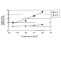
- FIG. 4 is a diagram illustrating an example of the relationship between the processing temperature and the amount of decrease in the photoresist height.
- FIG. 5 is a diagram illustrating an example of the relationship of the sum of LWR and LER with respect to the processing temperature.
- FIG. 6 is a diagram showing an example of the relationship of LWR, LER, and photoresist height with respect to the processing temperature.
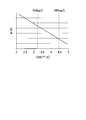
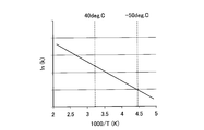
- FIG. 7 is a diagram illustrating an example of an Arrhenius plot in H 2 gas.
- FIG. 1 is a cross-sectional view showing an example of a plasma processing apparatus.
- FIG. 2 is a cross-sectional view showing an example of a semiconductor wafer.
- FIG. 3 is a flowchart illustrating
- FIG. 8 is a flowchart illustrating an example of a plasma processing method according to the second embodiment.
- FIG. 9 is a diagram illustrating an example of the relationship between the processing temperature and the selection ratio.
- FIG. 10 is a diagram illustrating an example of an Arrhenius plot for fluorine.
- FIG. 11 is a schematic diagram showing an example of the relationship between the processing temperature and the cross-sectional shape of the groove.
- FIG. 12 is a diagram illustrating an example of the relationship between the processing temperature and the taper angle.
- FIG. 13 is a flowchart illustrating an example of a plasma processing method according to the third embodiment.
- FIG. 14 is a diagram illustrating an example of the relationship between the processing temperature and Top-BtmCD.
- FIG. 15 is a diagram illustrating an example of an Arrhenius plot in O 2 gas.
- FIG. 16 is a diagram illustrating an example of the relationship between the processing temperature and the selection ratio.
- FIG. 17 is a flowchart illustrating an example of a plasma processing method according to the fourth embodiment.
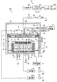
- FIG. 1 is a cross-sectional view illustrating an example of a plasma processing apparatus 100.
- the plasma processing apparatus 100 has a chamber 1 that is airtight and electrically grounded.
- the chamber 1 is formed in a substantially cylindrical shape by, for example, aluminum having an anodized surface.
- a shower head 16 is provided in the opening at the top of the chamber 1, and a cylindrical ground conductor 1 a is provided thereon.
- a mounting table 2 that horizontally supports a semiconductor wafer W that is an example of an object to be processed is provided.
- the mounting table 2 includes a base material 2 a and an electrostatic chuck 6.
- the base material 2a is made of a conductive metal such as aluminum and functions as a lower electrode.
- the base material 2a is supported by a support base 4 made of a conductor.
- the support 4 is supported on the bottom of the chamber 1 through the insulating plate 3.
- a focus ring 5 made of, for example, single crystal silicon is provided on the outer periphery above the mounting table 2.
- a cylindrical inner wall member 3 a made of, for example, quartz is provided around the mounting table 2 and the support table 4 so as to surround the mounting table 2 and the support table 4.
- An electrostatic chuck 6 is provided on the upper surface of the substrate 2a.
- the electrostatic chuck 6 includes an insulator 6b and an electrode 6a provided between the insulators 6b.
- the electrode 6 a is connected to the DC power supply 12.
- the electrostatic chuck 6 attracts and holds the semiconductor wafer W on the upper surface of the electrostatic chuck 6 by generating a Coulomb force on the surface of the electrostatic chuck 6 by a DC voltage applied to the electrode 6 a from the DC power source 12.
- the flow path 2b through which the refrigerant flows is formed inside the base material 2a.
- a refrigerant such as Galden circulates in the flow path 2b through the pipes 2c and 2d.
- the mounting table 2 and the electrostatic chuck 6 are controlled to a predetermined temperature by the refrigerant circulating in the flow path 2b.
- the mounting table 2 is provided with a pipe 30 for supplying a heat transfer gas (backside gas) such as helium gas to the back side of the semiconductor wafer W so as to penetrate the mounting table 2.
- the pipe 30 is connected to a backside gas supply source (not shown).
- the plasma processing apparatus 100 brings the semiconductor wafer W adsorbed and held on the upper surface of the electrostatic chuck 6 to a predetermined temperature by the coolant flowing in the flow path 2b and the heat transfer gas supplied to the back side of the semiconductor wafer W. Can be controlled.
- a shower head 16 is provided so as to face the mounting table 2 substantially in parallel, in other words, to face the semiconductor wafer W mounted on the mounting table 2. .
- the shower head 16 also functions as an upper electrode. That is, the shower head 16 and the mounting table 2 function as a pair of electrodes (upper electrode and lower electrode).
- a space between the semiconductor wafer W mounted on the mounting table 2 and the shower head 16 is referred to as a processing space S.
- a high frequency power supply 10a is connected to the shower head 16 via a matching unit 11a.
- a high frequency power source 10b is connected to the base material 2a of the mounting table 2 via a matching unit 11b.
- the high frequency power supply 10a applies high frequency power of a predetermined frequency (for example, 60 MHz) used for generating plasma to the shower head 16.
- the high-frequency power source 10b is a high-frequency power having a predetermined frequency used for ion attraction (bias), and a high-frequency power having a lower frequency (for example, 13 MHz) than the high-frequency power source 10a is applied to the substrate 2a of the mounting table 2. To do.
- the shower head 16 is supported on the upper portion of the chamber 1 through an insulating member 45.
- the shower head 16 includes a main body portion 16a and an upper top plate 16b.
- the main body portion 16a is formed of, for example, aluminum whose surface is anodized, and supports the upper top plate 16b in a detachable manner at the lower portion thereof.
- the upper top plate 16b is formed of a silicon-containing material such as quartz.
- Gas diffusion chambers 16c and 16d are provided in the main body 16a.
- a large number of gas flow ports 16e are formed at the bottom of the main body 16a so as to be positioned below the gas diffusion chamber 16c or 16d.
- the gas diffusion chamber 16c is provided in the approximate center of the shower head 16, and the gas diffusion chamber 16d is provided around the gas diffusion chamber 16c so as to surround the gas diffusion chamber 16c.
- the gas diffusion chambers 16c and 16d can independently control the flow rate of the processing gas.
- the upper top plate 16b is provided with gas flow ports 16f so as to penetrate the upper top plate 16b in the thickness direction, and each gas flow port 16f communicates with the gas flow port 16e described above. .
- the process gas supplied to the gas diffusion chambers 16c and 16d is diffused and supplied into the chamber 1 through the gas flow port 16e or 16f.
- the main body 16a and the like are provided with a temperature adjusting mechanism such as a heater (not shown) and a pipe (not shown) for circulating the refrigerant, so that the shower head 16 is within a desired range during the processing of the semiconductor wafer W.
- the temperature can be controlled.
- the main body 16a of the shower head 16 is provided with a gas inlet 16g for introducing a processing gas into the gas diffusion chamber 16c and a gas inlet 16h for introducing a processing gas into the gas diffusion chamber 16d.
- One end of a pipe 15a is connected to the gas inlet 16g.
- the other end of the pipe 15a is connected to a gas supply source 15 that supplies a gas used for processing the semiconductor wafer W through a valve V1 and a mass flow controller (MFC) 15c.
- MFC mass flow controller
- one end of a pipe 15b is connected to the gas inlet 16h.
- the other end of the pipe 15b is connected to the gas supply source 15 via the valve V2 and the MFC 15d.
- the processing gas supplied from the gas supply source 15 is supplied to the gas diffusion chambers 16c and 16d through the pipes 15a and 15b, respectively, and is diffused into the chamber 1 through the gas distribution ports 16e and 16f. Supplied.
- the gas supply source 15 supplies the reformed gas into the chamber 1 when, for example, a reforming process described later is executed.
- the shower head 16 is electrically connected to a variable DC power source 52 that outputs a negative DC voltage via a low-pass filter (LPF) 51 and a switch 53.
- the switch 53 controls application and interruption of the DC voltage from the variable DC power source 52 to the shower head 16. For example, when high frequency power is applied from the high frequency power source 10 a to the shower head 16 and high frequency power is applied from the high frequency power source 10 b to the mounting table 2, and plasma is generated in the processing space S in the chamber 1, Thus, the switch 53 is turned on, and a negative DC voltage of a predetermined magnitude is applied to the shower head 16 that functions as the upper electrode.
- An exhaust path 71 is provided around the mounting table 2 so as to surround the mounting table 2. Between the processing space S and the exhaust path 71, a baffle plate 18 having a plurality of through holes is provided around the mounting table 2 so as to surround the mounting table 2.
- An exhaust pipe 72 is connected to the exhaust path 71, and an exhaust device 73 is connected to the exhaust pipe 72.
- the exhaust device 73 includes a vacuum pump such as a turbo molecular pump. By operating the vacuum pump, the exhaust device 73 can reduce the pressure in the chamber 1 to a predetermined degree of vacuum via the exhaust path 71 and the exhaust pipe 72.
- An opening 74 is provided on the side wall of the chamber 1, and a gate valve G for opening and closing the opening 74 is provided in the opening 74.
- Depot shields 76 and 77 are detachably provided on the inner wall of the chamber 1 and the outer peripheral surface of the mounting table 2. The deposition shields 76 and 77 prevent etching by-products (deposition) from adhering to the inner wall of the chamber 1.
- a conductive member (GND block) 79 connected to the ground in a DC manner is provided at the position of the deposition shield 76 that is substantially the same height as the semiconductor wafer W held by suction on the electrostatic chuck 6.
- the GND block 79 suppresses abnormal discharge in the chamber 1.
- the operation of the plasma processing apparatus 100 configured as described above is comprehensively controlled by the control unit 60.
- the control unit 60 includes a CPU (Central Processing Unit) and a process controller 61 that controls each unit of the plasma processing apparatus 100, a user interface 62, and a storage unit 63.
- CPU Central Processing Unit
- the user interface 62 includes an input device such as a keyboard that is used to input commands for an operator to operate the plasma processing apparatus 100, and an output device such as a display that visualizes and displays the operating status of the plasma processing apparatus 100. .
- the storage unit 63 stores a control program (software) for realizing various processes executed by the plasma processing apparatus 100 under the control of the process controller 61, and a recipe storing process condition data. Yes.
- the process controller 61 operates based on a control program stored in the storage unit 63, and reads a recipe or the like from the storage unit 63 according to an instruction received via the user interface 62. Then, the process controller 61 controls the plasma processing apparatus 100 according to the read recipe or the like, whereby the plasma processing apparatus 100 performs a desired process.
- the process controller 61 may read a control program, a recipe, and the like stored in a computer-readable recording medium (for example, a hard disk, a CD, a flexible disk, a semiconductor memory, etc.) from the recording medium and execute the program. Is possible. Further, the process controller 61 can acquire and execute a control program, a recipe, and the like stored in the storage unit of another device from the other device, for example, via a communication line.
- a computer-readable recording medium for example, a hard disk, a CD, a flexible disk, a semiconductor memory, etc.
- control unit 60 controls each unit of the plasma processing apparatus 100 to perform a plasma processing method described later.
- the control unit 60 supplies a reformed gas into the chamber 1 when performing a reforming process described later, and a predetermined semiconductor wafer W held on the electrostatic chuck 6 by suction. Control to temperature.
- the control unit 60 applies high-frequency power having a predetermined frequency and a negative DC voltage having a predetermined voltage to the shower head 16 that functions as the upper electrode, and applies high-frequency power having a predetermined frequency to the mounting table 2 that functions as the lower electrode.
- plasma of the reformed gas is generated in the chamber 1.
- the control unit 60 modifies the photoresist provided on the semiconductor wafer W by the generated reformed gas plasma.
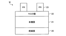
- FIG. 2 is a cross-sectional view showing an example of the semiconductor wafer W.
- the semiconductor wafer W is formed by laminating an organic film 21, a mask film 22, and a photoresist (PR) 23 in this order on the insulating film 20.
- the insulating film 20 is an oxide film such as SiO 2.
- the organic film 21 is an organic dielectric layer (ODL) such as a spin-on carbon film.
- the mask film 22 is, for example, a silicon-containing antireflection film (SiARC).
- the mask film 22 may have a two-layer structure in which a SiON film is stacked on the organic film 21 and an organic antireflection film (BARC) is stacked thereon.
- the photoresist 23 is, for example, an EUV resist in which a predetermined pattern is formed using EUV light.
- the photoresist 23 is an example of a resist film.
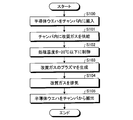
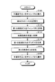
- FIG. 3 is a flowchart illustrating an example of the plasma processing method according to the first embodiment.
- the gate valve G is opened, and the semiconductor wafer W is carried into the chamber 1 from the opening 74 by a transfer robot (not shown) and placed on the electrostatic chuck 6. (S100). Then, the transfer robot retreats out of the chamber 1 and the gate valve G is closed. A predetermined DC voltage is applied to the electrode 6a of the electrostatic chuck 6 from the DC power source 12, and the semiconductor wafer W is attracted and held on the electrostatic chuck 6 by Coulomb force. Then, the inside of the chamber 1 is exhausted to a predetermined degree of vacuum by the vacuum pump of the exhaust device 73.
- the reformed gas is supplied into the chamber 1 from the gas supply source 15 at a predetermined flow rate, and the inside of the chamber 1 is maintained at a predetermined pressure (S101).
- the reformed gas is a hydrogen-containing gas.
- the reformed gas is a mixed gas containing, for example, Ar gas and H 2 gas.
- the reformed gas may be H2 gas, hydrogen halide gas, or a mixed gas containing a rare gas and H2 gas or hydrogen halide gas.
- the hydrogen halide gas for example, HBr gas or the like can be used.
- Ar gas etc. can be used, for example.
- the semiconductor wafer W is controlled to a predetermined processing temperature by the refrigerant flowing in the flow path 2b of the mounting table 2 and the heat transfer gas supplied to the back side of the semiconductor wafer W (S102).
- the plasma processing apparatus 100 controls the processing temperature of the semiconductor wafer W to ⁇ 20 ° C. or lower, for example.
- the plasma processing apparatus 100 controls the processing temperature of the semiconductor wafer W to a temperature within a range of ⁇ 60 ° C. or higher and ⁇ 20 ° C. or lower, for example.
- a high frequency power having a predetermined frequency (for example, 60 MHz) is applied to the shower head 16 from the high frequency power source 10a, and a negative DC voltage having a predetermined voltage is applied from the variable DC power source 52.
- high frequency power of a predetermined frequency (for example, 13 MHz) is applied to the mounting table 2 from the high frequency power supply 10b.
- an electric field is formed between the shower head 16 as the upper electrode and the mounting table 2 as the lower electrode, and plasma of the reformed gas is generated in the processing space S on the semiconductor wafer W (S103).
- Step S103 is an example of a reforming process.
- the surface of the photoresist 23 of the semiconductor wafer W is modified by the plasma of the modifying gas.
- LWR Line Width Roughness
- LER Line Edge Roughness
- the semiconductor wafer W by the plasma of the reformed gas After the processing of the semiconductor wafer W by the plasma of the reformed gas is performed for a predetermined time, the supply of the reformed gas from the gas supply source 15 is stopped, and the reformed gas in the chamber 1 is stopped by the vacuum pump of the exhaust device 73. Is exhausted (S104). Then, the gate valve G is opened, and the semiconductor wafer W on the electrostatic chuck 6 is unloaded from the chamber 1 by a transfer robot or the like (S105), and the plasma processing shown in this flowchart ends. After the plasma processing shown in this flowchart is performed, the semiconductor wafer W is subjected to processing for etching the mask film 22 using the photoresist 23 with improved LWR and LER as a mask.
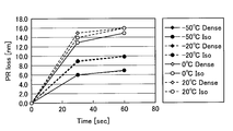
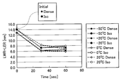
- FIG. 4 is a diagram illustrating an example of the relationship between the processing temperature and the amount of decrease in the photoresist height.
- FIG. 4 shows experimental results of the amount of decrease in the height of the photoresist 23 with respect to the time during which the semiconductor wafer W is exposed to plasma at each temperature from ⁇ 50 ° C. to + 20 ° C. Note that “Dense” shown in FIG. 4 indicates the amount of decrease in the height of the photoresist 23 in the region where the pattern density formed on the photoresist 23 is high, and “Iso” shown in FIG. The amount of reduction in the height of the photoresist 23 in the region where the density of the pattern formed on the photoresist 23 is low is shown.
- the lower the processing temperature of the semiconductor wafer W the smaller the decrease in the height of the photoresist 23 is. That is, the amount of decrease in the height of the photoresist 23 depends on the processing temperature of the semiconductor wafer W. Note that, even in a region where the pattern density formed on the photoresist 23 is high or a region where the pattern density formed on the photoresist 23 is low, the lower the processing temperature of the semiconductor wafer W, the lower the photoresist 23 height. The trend of small quantities remains the same.
- FIG. 5 is a diagram showing an example of the relationship of the sum of LWR and LER with respect to the processing temperature.
- FIG. 5 shows the experimental results of the sum of LWR and LER with respect to the time during which the semiconductor wafer W is exposed to plasma at each processing temperature from ⁇ 50 ° C. to + 20 ° C.
- the value of the sum of LWR and LER was measured in a region where the density of the pattern formed on the photoresist 23 is high and a region where the density of the pattern formed on the photoresist 23 is low.
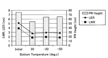
- the relationship between the LWR, LER, and photoresist height with respect to the processing temperature is summarized as shown in FIG. 6, for example.
- the first axis shows an example of the relationship between LWR and LER with respect to the processing temperature
- the second axis shows an example of the relationship between the photoresist height and the processing temperature.
- the lower the processing temperature of the semiconductor wafer W the smaller the amount of reduction in the height of the photoresist 23 is. Further, there is not much difference in the reduction in the height of the photoresist 23 between the case where the processing temperature of the semiconductor wafer W is ⁇ 20 ° C. and the case where it is ⁇ 50 ° C. This is presumably because there is a threshold value for the activation energy of H radicals in the vicinity of ⁇ 20 ° C. Therefore, if the processing temperature of the semiconductor wafer W is set to ⁇ 20 ° C. or lower, the amount of decrease in the height of the photoresist 23 can be reduced.
- the processing temperature of the semiconductor wafer W is in the range of ⁇ 60 ° C. or more and ⁇ 20 ° C. or less, it can be controlled to a temperature in that range using a commonly used refrigerant. An increase in cost in processing can also be suppressed.
- the height of the photoresist 23 decreases due to a spontaneous reaction by H radicals present in the plasma of the reformed gas.
- the rate constant k of the reaction in the H radical can be calculated by the Arrhenius equation (1) shown below.
- A is a constant (frequency factor) independent of temperature
- E a is activation energy per mole
- R is a gas constant
- T is an absolute temperature.
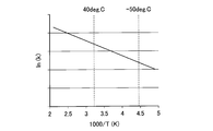
- FIG. 7 is a diagram illustrating an example of an Arrhenius plot in H 2 gas.
- the lower the treatment temperature that is, the higher the value of 1000 / T (K)
- the lower the value of the rate constant k of the H radical reaction and the lower the reaction rate. Therefore, it is considered that by reducing the processing temperature of the semiconductor wafer W, the rate of spontaneous reaction due to H radicals present in the plasma of the reformed gas is reduced, and the reduction in the height of the photoresist 23 can be suppressed.
- the LWR and LER of the photoresist 23 are improved by the effect of the VUV (Vacuum Ultra-Vioret) reaction.
- the photoresist 23 irradiated with the VUV light absorbs the VUV light, a chemical reaction occurs on the surface, and the surface flows. As a result, the surface of the photoresist 23 becomes smooth, and surface irregularities that cause LWR and LER are reduced.
- the VUV reaction depends on the emission intensity of VUV light.
- the emission intensity I of VUV light is expressed by, for example, the following formula (2). Where ⁇ and ⁇ are proportional constants, k ex (p) is an excitation rate coefficient, n (1) is a radical density, and ne is an electron density.
- the emission intensity I of VUV light in the reforming process depends on the density of H radicals but not on the temperature. Therefore, if the conditions other than the processing temperature of the semiconductor wafer W are the same, the LWR and LER improvement effects equivalent to those at room temperature or high temperature can be obtained even at low temperatures.
- Example 1 a reforming process for reforming the photoresist 23 of the semiconductor wafer W using a plasma of a reformed gas was performed.
- a first etching process for etching the mask film 22 is further performed using the photoresist 23 as a mask.
- the configuration of the plasma processing apparatus 100 is the same as that of the plasma processing apparatus 100 in the first embodiment shown in FIG.
- FIG. 8 is a flowchart illustrating an example of a plasma processing method according to the second embodiment. Note that in FIG. 8, the processes denoted by the same reference numerals as those in FIG. 3 are the same as the processes described in FIG.
- the gate valve G is opened, and the semiconductor wafer W is placed on the electrostatic chuck 6 and sucked and held on the electrostatic chuck 6 (S100). Then, the inside of the chamber 1 is exhausted to a predetermined degree of vacuum by the vacuum pump of the exhaust device 73. Then, the processes of steps S101 to S104 shown in FIG. 3 are executed.
- the first processing gas is supplied into the chamber 1 from the gas supply source 15 at a predetermined flow rate, and the interior of the chamber 1 is maintained at a predetermined pressure (S110).
- the first processing gas includes SF6 gas.
- the first processing gas may be a halogenated compound gas and may contain a gas containing a CF bond or SF bond.
- the first processing gas may contain CF4 gas, SF6 gas, or the like.
- the semiconductor wafer W is controlled to a predetermined processing temperature by the refrigerant flowing in the flow path 2b of the mounting table 2 and the heat transfer gas supplied to the back side of the semiconductor wafer W (S111).
- the plasma processing apparatus 100 controls the processing temperature of the semiconductor wafer W to a normal temperature (for example, a temperature within a range of 0 ° C. to 40 ° C.).
- a high frequency power having a predetermined frequency (for example, 60 MHz) is applied to the shower head 16 from the high frequency power source 10 a, and a negative DC voltage having a predetermined voltage is applied from the variable DC power source 52.
- high frequency power of a predetermined frequency (for example, 13 MHz) is applied to the mounting table 2 from the high frequency power supply 10b.
- an electric field is formed between the shower head 16 as the upper electrode and the mounting table 2 as the lower electrode, and plasma of the first processing gas is generated in the processing space S on the semiconductor wafer W (S112).
- the mask film 22 is etched by the plasma of the first processing gas using the photoresist 23 as a mask.
- Step S112 is an example of a first etching process.
- the supply of the first processing gas from the gas supply source 15 is stopped, and the first pump in the chamber 1 is turned on by the vacuum pump of the exhaust device 73. 1 processing gas is exhausted (S113). Then, the gate valve G is opened, the semiconductor wafer W on the electrostatic chuck 6 is unloaded from the chamber 1 (S105), and the plasma processing shown in this flowchart ends. After the plasma processing shown in this flowchart is performed, the semiconductor wafer W is subjected to processing for etching the photoresist 23 using the mask film 22 to which the pattern of the photoresist 23 is transferred by etching as a mask.
- the first processing gas is used for etching the mask film 22 using the photoresist 23 as a mask.
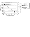
- the selection ratio of the mask film 22 to the photoresist 23 is measured, for example, as shown in FIG.
- FIG. 9 is a diagram illustrating an example of the relationship between the processing temperature and the selection ratio. Referring to FIG. 9, the selectivity when SF6 is used as the first processing gas is higher than the selectivity when CF4 is used. Further, the difference between the selection ratio when SF6 was used as the first processing gas and the selection ratio when CF4 was used was further increased in the normal temperature region (range of 0 ° C. to 40 ° C.).
- the selection ratio of the mask film 22 to the photoresist 23 is such that a by-product generated by the combination of the element contained in the first processing gas and the carbon contained in the photoresist 23 serves as a protective film. Improve by depositing on top. Since the bond energy of the CS bond is 272 (kJ / mol) and the bond energy of the CC bond is 346 (kJ / mol), the CS bond is less energy than the CC bond. Combine to make by-products. Therefore, when SF6 is used as the first processing gas, a by-product is more easily generated, and a protective film is more easily formed on the photoresist 23. Therefore, the selection ratio when SF6 is used as the first processing gas is higher than the selection ratio when CF4 is used.
- the mask film 22 has a double structure of SiARC or BARC and SiON. For this reason, the mask film 22 contains silicon element. Then, in the process of etching the mask film 22, a by-product generated by the combination of the element contained in the first processing gas and the silicon contained in the mask film 22 is formed on the photoresist 23 as a protective film. To deposit. This also improves the selectivity of the mask film 22 with respect to the photoresist 23.
- the Si—S bond is more than the Si—C bond. Bonds with less energy and produces by-products. Therefore, when SF6 is used as the first processing gas, a by-product is more easily generated, and a protective film is more easily formed on the photoresist 23. Therefore, the selection ratio when SF6 is used as the first processing gas is higher than the selection ratio when CF4 is used.
- both F radicals (F * ) and F ions (F + ) in the plasma contribute to the plasma etching of the mask film 22.
- the by-product that has reacted with the carbon contained in the mask film 22 forms a protective film on the side wall and bottom surface of the mask film 22. Therefore, the shape of the groove formed in the mask film 22 by plasma etching is determined by the correlation between the F ions contributing to the downward etching, the F radical contributing to the isotropic etching, and the protective film.
- the bond energy of SF bond is 284 (kJ / mol) and the bond energy of CF bond is 485 (kJ / mol)
- the case where SF6 is used as the first processing gas is used.
- the absolute amount of F radicals in the plasma is larger than the absolute amount of F radicals in the plasma when CF4 is used as the first processing gas. Therefore, when SF6 is used as the first processing gas, isotropic etching with F radicals is promoted more than when CF4 is used as the first processing gas.
- FIG. 10 shows an example of an Arrhenius plot for fluorine.
- the reaction rate constant k in fluorine increases as the treatment temperature increases, that is, as the value of 1000 / T (K) decreases, the value of the reaction rate constant k increases. Rises.
- the lower the treatment temperature that is, the higher the value of 1000 / T (K)
- FIG. 11 is a schematic diagram showing an example of the relationship between the processing temperature and the cross-sectional shape of the groove.
- FIG. 11A shows an example of the cross-sectional shape of the groove formed in the mask film 22 when etching is performed at a low processing temperature (for example, less than 0 ° C.).
- FIG. 11B shows an example of the cross-sectional shape of the groove formed in the mask film 22 when etching is performed at a processing temperature of room temperature (for example, 0 ° C. or higher and lower than 40 ° C.).
- FIG. 11C shows an example of the cross-sectional shape of the groove formed in the mask film 22 when etching is performed at a high processing temperature (for example, 40 ° C. or higher).
- the processing temperature is room temperature
- the balance between the protective film formed on the side wall of the groove and the isotropic etching by F radicals is good.
- the side wall of the groove formed in the film 22 has an angle close to vertical.
- FIG. 12 is a diagram showing an example of the relationship between the processing temperature and the taper angle.
- the angle of the sidewall of the groove increases as the processing temperature increases.
- the taper angle is 80 degrees or higher.
- the taper angle is 90 degrees when the process temperature is about 40 ° C. due to the tendency of the taper angle to increase with respect to the increase in process temperature. Become.
- the side wall of the groove formed in the mask film 22 is preferably at an angle in the range of 80 degrees or more and 90 degrees or less. Therefore, when SF6 is used as the first processing gas, if the processing temperature is in the range of 0 ° C. or more and 40 ° C. or less, the taper angle of the groove sidewall is in the range of 80 ° or more and 90 ° or less. Become. Accordingly, in the first etching step for etching the mask film 22, when SF6 is used as the first processing gas, the processing temperature is preferably in the range of 0 ° C. or higher and 40 ° C. or lower.
- the processing temperature is in the range of about 20 ° C. or more and 40 ° C. or less, the taper angle of the groove sidewall is 80 degrees or more and 90 degrees. The angle is within the following range. Therefore, when CF4 is used as the first processing gas in the first etching step for etching the mask film 22, the processing temperature is preferably in the range of 20 ° C. or higher and 40 ° C. or lower.
- the mask film 22 of the semiconductor wafer W is etched using the photoresist 23 as a mask.
- One etching step was performed.
- the mask film 22 etched in the first etching process is used as a mask, and the organic film 21 of the semiconductor wafer W is further used.
- a second etching step for etching is performed.
- the configuration of the plasma processing apparatus 100 is the same as that of the plasma processing apparatus 100 in the first embodiment shown in FIG.
- FIG. 13 is a flowchart illustrating an example of a plasma processing method according to the third embodiment.
- the processes denoted by the same reference numerals as those in FIG. 3 or FIG. 8 are the same as the processes described in FIG. 3 or FIG.
- the gate valve G is opened, and the semiconductor wafer W is placed on the electrostatic chuck 6 and sucked and held on the electrostatic chuck 6 (S100). Then, the inside of the chamber 1 is exhausted to a predetermined degree of vacuum by the vacuum pump of the exhaust device 73.
- steps S101 to S104 shown in FIG. 3 is executed. Thereby, the photoresist 23 is modified and LWR and LER of the photoresist 23 are reduced.
- steps S110 to S113 shown in FIG. 8 are executed. As a result, the pattern of the photoresist 23 in which LWR and LER are reduced is transferred to the mask film 22.
- the second processing gas is supplied into the chamber 1 from the gas supply source 15 at a predetermined flow rate, and the interior of the chamber 1 is maintained at a predetermined pressure (S120).
- the second processing gas is a mixed gas of Ar gas and O 2 gas.
- the second processing gas may be a mixed gas of a rare gas and a gas containing oxygen atoms.
- Ar gas can be used.
- the gas containing oxygen atoms for example, CO2 gas or the like can be used in addition to O2 gas.
- the semiconductor wafer W is controlled to a predetermined processing temperature by the refrigerant flowing in the flow path 2b of the mounting table 2 and the heat transfer gas supplied to the back side of the semiconductor wafer W (S121).
- the plasma processing apparatus 100 controls the processing temperature of the semiconductor wafer W to ⁇ 20 ° C. or lower, for example.
- the plasma processing apparatus 100 controls the processing temperature of the semiconductor wafer W to a temperature within a range of ⁇ 60 ° C. or higher and ⁇ 20 ° C. or lower, for example.
- a high frequency power having a predetermined frequency (for example, 60 MHz) is applied to the shower head 16 from the high frequency power source 10 a, and a negative DC voltage having a predetermined voltage is applied from the variable DC power source 52.
- high frequency power of a predetermined frequency (for example, 13 MHz) is applied to the mounting table 2 from the high frequency power supply 10b.
- an electric field is formed between the shower head 16 as the upper electrode and the mounting table 2 as the lower electrode, and plasma of the second processing gas is generated in the processing space S on the semiconductor wafer W (S122).
- the organic film 21 is etched by the plasma of the second processing gas using the mask film 22 to which the pattern of the photoresist 23 is transferred as a mask.
- Step S122 is an example of a second etching process.
- the supply of the second processing gas from the gas supply source 15 is stopped, and the vacuum pump of the exhaust device 73 is used to supply the second processing gas in the chamber 1.
- the second processing gas is exhausted (S123).
- the gate valve G is opened, the semiconductor wafer W on the electrostatic chuck 6 is unloaded from the chamber 1 (S105), and the plasma processing shown in this flowchart ends.
- the semiconductor wafer W is subjected to processing for etching the insulating film 20 using the organic film 21 to which the pattern of the mask film 22 is transferred by etching as a mask.
- the second processing gas is used for etching the organic film 21 using the mask film 22 as a mask.
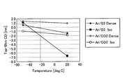
- a mixed gas of Ar gas and O 2 gas is used as the second processing gas, for example, as shown in FIG. 14, the value of Top-BtmCD increases as the processing temperature of the semiconductor wafer W decreases.
- FIG. 14 is a diagram illustrating an example of the relationship between the processing temperature and Top-BtmCD.
- the vertical axis represents the Top-BtmCD value
- the horizontal axis represents the processing temperature of the semiconductor wafer W.
- Top-BtmCD is a value obtained by subtracting BtmCD from TopCD.
- TopCD is a CD (Critical Dimension) at the opening of the groove formed in the organic film 21, and BtmCD is a CD at the bottom of the groove formed in the organic film 21.
- “Dense” shown in FIG. 14 indicates the Top-BtmCD of the groove in the region where the density of the groove formed in the organic film 21 is high, and “Iso” indicates the groove formed in the organic film 21.
- the Top-BtmCD of the groove in the low density region is shown.
- Top-BtmCD When the value of Top-BtmCD is greater than 0, the side wall of the groove formed in the organic film 21 is tapered. When the Top-BtmCD value is smaller than 0, the sidewall of the groove formed in the organic film 21 has a bowing shape. When the Top-BtmCD value is 0, the side wall of the groove formed in the organic film 21 is substantially vertical.
- the value of Top-BtmCD increases in the negative direction as the processing temperature of the semiconductor wafer W increases. That is, as the processing temperature of the semiconductor wafer W increases, the groove formed in the organic film 21 becomes a bowing shape.
- the Top-BtmCD value approaches 0 as the processing temperature of the semiconductor wafer W decreases. That is, the lower the processing temperature of the semiconductor wafer W, the more the bowing shape of the groove formed in the organic film 21 is suppressed.
- the value of Top-BtmCD approaches 0 as the processing temperature of the semiconductor wafer W decreases. That is, the lower the processing temperature of the semiconductor wafer W, the more the bowing shape of the groove formed in the organic film 21 is suppressed. Therefore, even when a mixed gas of Ar gas and CO 2 gas is used as the second processing gas, the bowing shape of the groove formed in the organic film 21 is suppressed by setting the processing temperature of the semiconductor wafer W low. Can do.
- FIG. 15 is a diagram showing an example of an Arrhenius plot for O 2 gas.
- the processing temperature that is, the value of 1000 / T (K) is decreased
- the value of the rate constant k of the reaction such as O radical is increased and the reaction rate is increased. That is, the higher the processing temperature, the higher the reaction rate of O radicals contributing to isotropic etching, the spontaneous reaction of the side wall of the groove formed in the organic film 21 is promoted, and the groove has a bowing shape.
- the processing temperature when the processing temperature is lowered, that is, the value of 1000 / T (K) is increased, the value of the rate constant k of the reaction such as O radical is decreased and the reaction rate is decreased. . That is, the lower the processing temperature, the lower the reaction rate of O radicals contributing to isotropic etching, the spontaneous reaction of the side walls of the grooves formed in the organic film 21 is suppressed, and the bowing shape of the grooves is suppressed. Therefore, in the etching of the organic film 21 using the mask film 22 as a mask, the bowing shape of the groove formed in the organic film 21 can be suppressed by setting the processing temperature of the semiconductor wafer W low.
- the processing temperature of the semiconductor wafer W is about ⁇ 20 ° C. or lower, the Top-BtmCD value is ⁇ 2.0 nm or higher under any condition, and the bowing shape of the groove is sufficiently suppressed. Is done. Therefore, in the etching of the organic film 21 using the mask film 22 as a mask, when the mixed gas of Ar gas and O 2 gas or the mixed gas of Ar gas and CO 2 gas is used as the second processing gas, the processing of the semiconductor wafer W is performed.
- the temperature is preferably set to ⁇ 20 ° C. or lower.
- the value is +2.0 nm or more. If the value of Top-BtmCD becomes too large in the positive direction, the side wall of the groove formed in the organic film 21 may be tapered, and the bottom may be blocked to cause an etch stop. Therefore, in the etching of the organic film 21 using the mask film 22 as a mask, when the mixed gas of Ar gas and O 2 gas or the mixed gas of Ar gas and CO 2 gas is used as the second processing gas, the processing of the semiconductor wafer W is performed.
- the temperature is more preferably set to a temperature in the range of ⁇ 60 ° C. or more and ⁇ 20 ° C. or less.
- FIG. 16 is a diagram illustrating an example of the relationship between the processing temperature and the selection ratio.
- SiARC is used as the mask film 22.
- the etching rate of the mask film 22 has little dependence on the processing temperature of the semiconductor wafer W, but the etching rate of the organic film 21 increases as the processing temperature of the semiconductor wafer W decreases. Therefore, the lower the processing temperature of the semiconductor wafer W, the higher the selectivity of the organic film 21 with respect to the mask film 22. Therefore, in the etching of the organic film 21 using the mask film 22 as a mask, the organic film 21 can be etched with a high selectivity by setting the processing temperature of the semiconductor wafer W low.
- Example 3 the modification process, the first etching process, and the second etching process were performed in the same plasma processing apparatus 100. In contrast, in this embodiment, the modification process and the second etching process are performed in the first plasma processing apparatus 100, and the first etching process is performed in the second plasma processing apparatus 100. Different from Example 3. In the present embodiment, the configuration of the first plasma processing apparatus 100 and the second plasma processing apparatus 100 is the same as that of the plasma processing apparatus 100 in the first embodiment shown in FIG. To do.
- FIG. 17 is a flowchart illustrating an example of a plasma processing method according to the fourth embodiment.
- the gate valve G is opened, and the semiconductor wafer W is loaded into the chamber 1 from the opening 74 by a transfer robot or the like and placed on the electrostatic chuck 6 (S200). ).
- the gate valve G is closed, and the semiconductor wafer W is attracted and held by the electrostatic chuck 6.
- the inside of the chamber 1 is exhausted to a predetermined degree of vacuum by the vacuum pump of the exhaust device 73.
- the reformed gas is supplied into the chamber 1 from the gas supply source 15 at a predetermined flow rate, and the inside of the chamber 1 is maintained at a predetermined pressure.
- the reformed gas is a hydrogen-containing gas.
- the reformed gas includes, for example, Ar gas and H 2 gas.
- the reformed gas may be H2 gas, hydrogen halide gas, or a mixed gas containing a rare gas and H2 gas or hydrogen halide gas.
- the semiconductor wafer W is controlled to a predetermined processing temperature by the refrigerant flowing in the flow path 2b of the mounting table 2 and the heat transfer gas supplied to the back side of the semiconductor wafer W (S202).
- the plasma processing apparatus 100 controls the processing temperature of the semiconductor wafer W to ⁇ 20 ° C. or lower, for example.
- the plasma processing apparatus 100 controls the processing temperature of the semiconductor wafer W to a temperature in the range of ⁇ 60 ° C. or higher and ⁇ 20 ° C. or lower, for example.
- Step S203 is an example of a reforming process.
- the surface of the photoresist 23 of the semiconductor wafer W is modified by the reformed gas plasma, and LWR and LER are improved.
- the supply of the reformed gas from the gas supply source 15 is stopped, and the reformed gas in the chamber 1 is stopped by the vacuum pump of the exhaust device 73. Is exhausted (S204). Then, in the first plasma processing apparatus 100, the gate valve G is opened, and the semiconductor wafer W on the electrostatic chuck 6 is unloaded from the chamber 1 by a transfer robot or the like (S205).
- the gate valve G is opened, and in step S205, the semiconductor wafer W unloaded from the first plasma processing apparatus 100 is transferred to the second plasma processing apparatus 100 by a transfer robot or the like. It is carried into the chamber 1 and placed on the electrostatic chuck 6 (S300). Then, the gate valve G is closed, and the semiconductor wafer W is attracted and held by the electrostatic chuck 6. Then, the inside of the chamber 1 is exhausted to a predetermined degree of vacuum by the vacuum pump of the exhaust device 73.
- the first processing gas is supplied into the chamber 1 from the gas supply source 15 at a predetermined flow rate, and the inside of the chamber 1 has a predetermined pressure.
- the first processing gas includes SF6 gas.
- the first processing gas may be a halogenated compound gas and may contain a gas containing a CF bond or SF bond.
- the semiconductor wafer W is controlled to a predetermined processing temperature by the refrigerant flowing in the flow path 2b of the mounting table 2 and the heat transfer gas supplied to the back side of the semiconductor wafer W (S302).
- the plasma processing apparatus 100 controls the processing temperature of the semiconductor wafer W to a normal temperature (for example, a temperature in the range of 0 ° C. to 40 ° C.).
- Step S303 is an example of a first etching process.
- the supply of the first processing gas from the gas supply source 15 is stopped, and the first pump in the chamber 1 is turned on by the vacuum pump of the exhaust device 73. 1 processing gas is exhausted (S304). Then, in the second plasma processing apparatus 100, the gate valve G is opened, and the semiconductor wafer W on the electrostatic chuck 6 is unloaded from the chamber 1 (S305).
- step S305 the semiconductor wafer W unloaded from the second plasma processing apparatus 100 is transferred to the first plasma processing apparatus 100 by a transfer robot or the like. It is carried into the chamber 1 and placed on the electrostatic chuck 6 (S206). Then, the gate valve G is closed, and the semiconductor wafer W is attracted and held by the electrostatic chuck 6. Then, the inside of the chamber 1 is exhausted to a predetermined degree of vacuum by the vacuum pump of the exhaust device 73.
- the second processing gas is supplied into the chamber 1 from the gas supply source 15 at a predetermined flow rate, and the inside of the chamber 1 has a predetermined pressure.
- the second processing gas is a mixed gas of Ar gas and O 2 gas.
- the second processing gas may be a mixed gas of a rare gas and a gas containing oxygen atoms.
- step S208 the plasma processing apparatus 100 controls the processing temperature of the semiconductor wafer W to ⁇ 20 ° C. or lower, for example.
- the plasma processing apparatus 100 controls the processing temperature of the semiconductor wafer W to a temperature in the range of ⁇ 60 ° C. or higher and ⁇ 20 ° C. or lower, for example.
- a high frequency power having a predetermined frequency and a negative DC voltage having a predetermined voltage are applied to the shower head 16, and a high frequency power having a predetermined frequency is applied to the mounting table 2.
- an electric field is formed between the shower head 16 as the upper electrode and the mounting table 2 as the lower electrode, and plasma of the second processing gas is generated in the processing space S on the semiconductor wafer W (S209).
- the organic film 21 is etched by the plasma of the second processing gas using the mask film 22 as a mask.
- Step S209 is an example of a second etching process.
- the supply of the second processing gas from the gas supply source 15 is stopped, and the vacuum pump of the exhaust device 73 is used to supply the second processing gas in the chamber 1.
- the second processing gas is exhausted (S210).
- the gate valve G is opened, the semiconductor wafer W on the electrostatic chuck 6 is unloaded from the chamber 1 (S211), and the plasma processing shown in this flowchart ends.
- the semiconductor wafer W is subjected to processing for etching the insulating film 20 using the organic film 21 to which the pattern of the mask film 22 is transferred by etching as a mask.
- the first plasma processing apparatus 100 performs the modification process (step S203) and the second etching process (step S209), and the second plasma processing apparatus 100 performs the first etching process. Execute. Then, the first plasma processing apparatus 100 controls the processing temperature of the semiconductor wafer W to, for example, ⁇ 20 ° C. or lower in the modification process and the second etching process, and the second plasma processing apparatus 100 In the etching process, the processing temperature of the semiconductor wafer W is controlled to, for example, room temperature.
- the first etching process is started after the modification process is performed at a processing temperature of ⁇ 20 ° C. or lower. Before starting, it is necessary to wait until the semiconductor wafer W and each part in the chamber 1 reach room temperature. Further, when the first etching process and the second etching process are continuously performed in one plasma processing apparatus 100, after the first etching process is performed at room temperature and before the second etching process is started. It is necessary to wait until the temperature of each part in the semiconductor wafer W and the chamber 1 becomes ⁇ 20 ° C. or lower.
- the modification process and the second etching process performed at ⁇ 20 ° C. or less are performed by the first plasma processing apparatus 100, and the first etching process performed at room temperature is performed by the second process.
- This is executed by the plasma processing apparatus 100.
- each process can be performed while keeping the inside of each plasma processing apparatus 100 at a predetermined temperature. Therefore, it is possible to reduce the waiting time until each part in the chamber 1 of the plasma processing apparatus 100 reaches a predetermined temperature. Further, it is possible to improve the throughput when the modifying process, the first etching process, and the second etching process are successively performed on the plurality of semiconductor wafers W.
- the second plasma processing apparatus 100 performs the processing shown in step S302 while the processing shown in steps S200 to S205 is being performed in the first plasma processing apparatus 100. May be performed first. Thereby, a 1st etching process can be started more rapidly.
Landscapes
- Engineering & Computer Science (AREA)
- Physics & Mathematics (AREA)
- Power Engineering (AREA)
- Condensed Matter Physics & Semiconductors (AREA)
- General Physics & Mathematics (AREA)
- Manufacturing & Machinery (AREA)
- Computer Hardware Design (AREA)
- Microelectronics & Electronic Packaging (AREA)
- Chemical & Material Sciences (AREA)
- Plasma & Fusion (AREA)
- Chemical Kinetics & Catalysis (AREA)
- General Chemical & Material Sciences (AREA)
- Inorganic Chemistry (AREA)
- Electromagnetism (AREA)
- Spectroscopy & Molecular Physics (AREA)
- Analytical Chemistry (AREA)
- Drying Of Semiconductors (AREA)
- Plasma Technology (AREA)
Abstract
Description
図1は、プラズマ処理装置100の一例を示す断面図である。プラズマ処理装置100は、気密に構成され、電気的に接地電位とされたチャンバ1を有する。チャンバ1は、例えば表面に陽極酸化処理が施されたアルミニウム等により、略円筒状に形成される。チャンバ1の上部の開口には、シャワーヘッド16が設けられ、その上には、円筒状の接地導体1aが設けられている。チャンバ1内には、被処理体の一例である半導体ウエハWを水平に支持する載置台2が設けられている。
本実施例において処理される半導体ウエハWは、例えば図2に示すような構造である。図2は、半導体ウエハWの一例を示す断面図である。半導体ウエハWは、絶縁膜20上に、有機膜21、マスク膜22、およびフォトレジスト(PR)23が、この順に積層されて形成される。絶縁膜20は、例えばSiO2等の酸化膜である。有機膜21は、例えばスピンオンカーボン膜等の有機誘電体層(ODL:Organic Dielectric Layer)である。マスク膜22は、例えばシリコン含有反射防止膜(SiARC)である。なお、他の例として、マスク膜22は、有機膜21上にSiON膜が積層され、その上に有機反射防止膜(BARC)が積層された2層構造であってもよい。フォトレジスト23は、例えば、EUV光を用いて所定のパターンが形成されたEUVレジストである。フォトレジスト23は、レジスト膜の一例である。
次に、図2に示した半導体ウエハWに対して行われるプラズマ処理について説明する。図3は、実施例1におけるプラズマ処理方法の一例を示すフローチャートである。

図8は、実施例2におけるプラズマ処理方法の一例を示すフローチャートである。なお、図8において、図3と同一の符号を付した処理は、図3において説明した処理と同様であるため、詳細な説明を省略する。
図13は、実施例3におけるプラズマ処理方法の一例を示すフローチャートである。なお、図13において、図3または図8と同一の符号を付した処理は、図3または図8において説明した処理と同様であるため、詳細な説明を省略する。
図17は、実施例4におけるプラズマ処理方法の一例を示すフローチャートである。まず、第1のプラズマ処理装置100において、ゲートバルブGが開かれ、半導体ウエハWが搬送ロボット等により、開口部74からチャンバ1内に搬入され、静電チャック6上に載置される(S200)。そして、ゲートバルブGが閉じられ、半導体ウエハWが静電チャック6に吸着保持される。そして、排気装置73の真空ポンプによりチャンバ1内が所定の真空度まで排気される。
100 プラズマ処理装置
1 チャンバ
2 載置台
16 シャワーヘッド
20 絶縁膜
21 有機膜
22 マスク膜
23 フォトレジスト
Claims (6)
- 有機膜、マスク膜、およびレジスト膜が順に積層された被処理体をプラズマにより処理するプラズマ処理方法であって、
前記レジスト膜に所定のパターンが形成された前記被処理体が搬入されたチャンバ内にH2ガス、ハロゲン化水素ガス、または、希ガスとH2ガスまたはハロゲン化水素ガスとを含む混合ガスである改質ガスを供給する工程と、
-20℃以下の処理温度で、前記改質ガスのプラズマにより前記被処理体の前記レジスト膜を改質する改質工程と
を有することを特徴とするプラズマ処理方法。 - 前記チャンバ内にエッチング用の第1の処理ガスを供給する工程と、
0℃以上40℃以下の範囲内の処理温度で、前記第1の処理ガスのプラズマにより、前記改質工程で改質された前記レジスト膜をマスクとして、前記マスク膜をエッチングする第1のエッチング工程と
を有することを特徴とする請求項1に記載のプラズマ処理方法。 - 前記第1の処理ガスには、
ハロゲン化化合物ガスであって、CF結合またはSF結合を含むガスが含まれることを特徴とする請求項2に記載のプラズマ処理方法。 - 前記チャンバ内にエッチング用の第2の処理ガスを供給する工程と、
-20℃以下の処理温度で、前記第2の処理ガスのプラズマにより、前記第1のエッチング工程でエッチングされた前記マスク膜をマスクとして、前記有機膜をエッチングする第2のエッチング工程と
を有することを特徴とする請求項2または3に記載のプラズマ処理方法。 - 前記チャンバ内にエッチング用の第2の処理ガスを供給する工程と、
-20℃以下の処理温度で、前記第2の処理ガスのプラズマにより、前記改質工程で改質された前記レジスト膜のパターンが転写された前記マスク膜をマスクとして、前記有機膜をエッチングする第2のエッチング工程と
を有することを特徴とする請求項1に記載のプラズマ処理方法。 - 前記第2の処理ガスには、
希ガスと酸素原子を含むガスとの混合ガスが含まれることを特徴とする請求項4または5に記載のプラズマ処理方法。
Priority Applications (3)
| Application Number | Priority Date | Filing Date | Title |
|---|---|---|---|
| US15/747,900 US10460963B2 (en) | 2015-08-27 | 2016-08-10 | Plasma processing method |
| KR1020187002353A KR102608178B1 (ko) | 2015-08-27 | 2016-08-10 | 플라즈마 처리 방법 |
| CN201680043730.7A CN108028196A (zh) | 2015-08-27 | 2016-08-10 | 等离子体处理方法 |
Applications Claiming Priority (2)
| Application Number | Priority Date | Filing Date | Title |
|---|---|---|---|
| JP2015167416A JP6817692B2 (ja) | 2015-08-27 | 2015-08-27 | プラズマ処理方法 |
| JP2015-167416 | 2015-08-27 |
Publications (1)
| Publication Number | Publication Date |
|---|---|
| WO2017033754A1 true WO2017033754A1 (ja) | 2017-03-02 |
Family
ID=58100040
Family Applications (1)
| Application Number | Title | Priority Date | Filing Date |
|---|---|---|---|
| PCT/JP2016/073648 WO2017033754A1 (ja) | 2015-08-27 | 2016-08-10 | プラズマ処理方法 |
Country Status (6)
| Country | Link |
|---|---|
| US (1) | US10460963B2 (ja) |
| JP (1) | JP6817692B2 (ja) |
| KR (1) | KR102608178B1 (ja) |
| CN (1) | CN108028196A (ja) |
| TW (1) | TWI692029B (ja) |
| WO (1) | WO2017033754A1 (ja) |
Cited By (1)
| Publication number | Priority date | Publication date | Assignee | Title |
|---|---|---|---|---|
| US11189469B2 (en) * | 2018-03-30 | 2021-11-30 | Tokyo Electron Limited | Etching method and plasma processing apparatus |
Families Citing this family (8)
| Publication number | Priority date | Publication date | Assignee | Title |
|---|---|---|---|---|
| KR102632799B1 (ko) * | 2017-12-18 | 2024-02-01 | 도쿄엘렉트론가부시키가이샤 | 리소그래피를 위한 표면 접착력을 강화하기 위한 플라즈마 처리 방법 |
| KR20210076999A (ko) | 2018-11-14 | 2021-06-24 | 램 리써치 코포레이션 | 차세대 리소그래피에서 유용한 하드 마스크들을 제조하기 위한 방법들 |
| JP7229750B2 (ja) | 2018-12-14 | 2023-02-28 | 東京エレクトロン株式会社 | プラズマ処理方法およびプラズマ処理装置 |
| JP2020177958A (ja) * | 2019-04-15 | 2020-10-29 | 東京エレクトロン株式会社 | 基板処理方法及び基板処理装置 |
| CN112103166A (zh) * | 2019-06-18 | 2020-12-18 | 东京毅力科创株式会社 | 基板处理装置 |
| KR102539806B1 (ko) | 2020-01-15 | 2023-06-05 | 램 리써치 코포레이션 | 포토레지스트 부착 및 선량 감소를 위한 하부층 |
| KR20230041688A (ko) * | 2020-06-22 | 2023-03-24 | 램 리써치 코포레이션 | 금속-함유 포토레지스트 (photoresist) 증착을 위한 표면 개질 |
| JP2022163526A (ja) * | 2021-04-14 | 2022-10-26 | 東京エレクトロン株式会社 | 基板処理方法 |
Citations (6)
| Publication number | Priority date | Publication date | Assignee | Title |
|---|---|---|---|---|
| JPH06168918A (ja) * | 1992-11-30 | 1994-06-14 | Sony Corp | ドライエッチング方法及びドライエッチング装置 |
| JP2000221698A (ja) * | 1999-01-29 | 2000-08-11 | Sony Corp | 電子装置の製造方法 |
| JP2005072518A (ja) * | 2003-08-28 | 2005-03-17 | Hitachi Ltd | 半導体装置の製造方法およびその装置 |
| JP2005243681A (ja) * | 2004-02-24 | 2005-09-08 | Tokyo Electron Ltd | 膜改質方法、膜改質装置及びスリミング量の制御方法 |
| JP2009267352A (ja) * | 2008-03-31 | 2009-11-12 | Tokyo Electron Ltd | プラズマ処理方法及びコンピュータ読み取り可能な記憶媒体 |
| JP2014082475A (ja) * | 2012-09-25 | 2014-05-08 | Tokyo Electron Ltd | プラズマ処理方法 |
Family Cites Families (14)
| Publication number | Priority date | Publication date | Assignee | Title |
|---|---|---|---|---|
| JP4260764B2 (ja) * | 1999-03-09 | 2009-04-30 | 東京エレクトロン株式会社 | 半導体装置の製造方法 |
| JP4194521B2 (ja) * | 2004-04-07 | 2008-12-10 | 東京エレクトロン株式会社 | 半導体装置の製造方法 |
| WO2008096752A1 (ja) * | 2007-02-09 | 2008-08-14 | Tokyo Electron Limited | エッチング方法および記憶媒体 |
| JP4919871B2 (ja) * | 2007-02-09 | 2012-04-18 | 東京エレクトロン株式会社 | エッチング方法、半導体装置の製造方法および記憶媒体 |
| JP2008218867A (ja) * | 2007-03-07 | 2008-09-18 | Elpida Memory Inc | 半導体装置の製造方法 |
| JP2010205967A (ja) * | 2009-03-04 | 2010-09-16 | Tokyo Electron Ltd | プラズマエッチング方法、プラズマエッチング装置及びコンピュータ記憶媒体 |
| JP5606060B2 (ja) * | 2009-12-24 | 2014-10-15 | 東京エレクトロン株式会社 | エッチング方法及びエッチング処理装置 |
| JP2011138871A (ja) * | 2009-12-28 | 2011-07-14 | Renesas Electronics Corp | 半導体装置の製造方法 |
| EP2608247A1 (en) * | 2011-12-21 | 2013-06-26 | Imec | EUV photoresist encapsulation |
| JP5894106B2 (ja) * | 2012-06-18 | 2016-03-23 | 信越化学工業株式会社 | レジスト下層膜形成用化合物、これを用いたレジスト下層膜材料、レジスト下層膜形成方法、パターン形成方法 |
| JP6185305B2 (ja) * | 2013-06-28 | 2017-08-23 | 東京エレクトロン株式会社 | プラズマエッチング方法およびプラズマエッチング装置 |
| US9793127B2 (en) * | 2013-11-13 | 2017-10-17 | Taiwan Semiconductor Manufacturing Company Limited | Plasma generation and pulsed plasma etching |
| JP2015138914A (ja) * | 2014-01-23 | 2015-07-30 | マイクロン テクノロジー, インク. | 半導体装置の製造方法 |
| TWI653507B (zh) * | 2014-02-07 | 2019-03-11 | 比利時商愛美科公司 | 用於減低微影製程後線寬粗糙度之電漿方法 |
-
2015
- 2015-08-27 JP JP2015167416A patent/JP6817692B2/ja active Active
-
2016
- 2016-08-10 US US15/747,900 patent/US10460963B2/en active Active
- 2016-08-10 CN CN201680043730.7A patent/CN108028196A/zh active Pending
- 2016-08-10 WO PCT/JP2016/073648 patent/WO2017033754A1/ja active Application Filing
- 2016-08-10 KR KR1020187002353A patent/KR102608178B1/ko active IP Right Grant
- 2016-08-17 TW TW105126157A patent/TWI692029B/zh active
Patent Citations (6)
| Publication number | Priority date | Publication date | Assignee | Title |
|---|---|---|---|---|
| JPH06168918A (ja) * | 1992-11-30 | 1994-06-14 | Sony Corp | ドライエッチング方法及びドライエッチング装置 |
| JP2000221698A (ja) * | 1999-01-29 | 2000-08-11 | Sony Corp | 電子装置の製造方法 |
| JP2005072518A (ja) * | 2003-08-28 | 2005-03-17 | Hitachi Ltd | 半導体装置の製造方法およびその装置 |
| JP2005243681A (ja) * | 2004-02-24 | 2005-09-08 | Tokyo Electron Ltd | 膜改質方法、膜改質装置及びスリミング量の制御方法 |
| JP2009267352A (ja) * | 2008-03-31 | 2009-11-12 | Tokyo Electron Ltd | プラズマ処理方法及びコンピュータ読み取り可能な記憶媒体 |
| JP2014082475A (ja) * | 2012-09-25 | 2014-05-08 | Tokyo Electron Ltd | プラズマ処理方法 |
Cited By (1)
| Publication number | Priority date | Publication date | Assignee | Title |
|---|---|---|---|---|
| US11189469B2 (en) * | 2018-03-30 | 2021-11-30 | Tokyo Electron Limited | Etching method and plasma processing apparatus |
Also Published As
| Publication number | Publication date |
|---|---|
| KR20180043784A (ko) | 2018-04-30 |
| JP6817692B2 (ja) | 2021-01-20 |
| TWI692029B (zh) | 2020-04-21 |
| CN108028196A (zh) | 2018-05-11 |
| TW201719748A (zh) | 2017-06-01 |
| US10460963B2 (en) | 2019-10-29 |
| JP2017045869A (ja) | 2017-03-02 |
| KR102608178B1 (ko) | 2023-11-30 |
| US20180226279A1 (en) | 2018-08-09 |
Similar Documents
| Publication | Publication Date | Title |
|---|---|---|
| WO2017033754A1 (ja) | プラズマ処理方法 | |
| EP2819151B1 (en) | Plasma etching method and plasma etching apparatus | |
| US20100224587A1 (en) | Plasma etching method, plasma etching apparatus and computer-readable storage medium | |
| JP4912907B2 (ja) | プラズマエッチング方法及びプラズマエッチング装置 | |
| US20090203218A1 (en) | Plasma etching method and computer-readable storage medium | |
| US8609549B2 (en) | Plasma etching method, plasma etching apparatus, and computer-readable storage medium | |
| JP6255187B2 (ja) | シリコン酸化膜をエッチングする方法 | |
| US10453699B2 (en) | Etching method and etching apparatus | |
| US10580655B2 (en) | Plasma etching method for selectively etching silicon oxide with respect to silicon nitride | |
| KR101540816B1 (ko) | 플라즈마 에칭 방법, 컴퓨터 기억 매체 및 플라즈마 에칭 장치 | |
| JP2014096500A (ja) | プラズマエッチング方法及びプラズマエッチング装置 | |
| KR20150043978A (ko) | 플라즈마 처리 방법 | |
| US20220059361A1 (en) | Etching method and plasma processing apparatus | |
| US20080014755A1 (en) | Plasma etching method and computer-readable storage medium | |
| US9754797B2 (en) | Etching method for selectively etching silicon oxide with respect to silicon nitride | |
| US20070212887A1 (en) | Plasma etching method, plasma etching apparatus, control program and computer-readable storage medium | |
| KR20160110153A (ko) | 플라즈마 에칭 방법 및 플라즈마 에칭 장치 | |
| US9633864B2 (en) | Etching method | |
| US20070197040A1 (en) | Plasma etching method, plasma etching apparatus, control program and computer-readable storage medium | |
| WO2022196369A1 (ja) | 基板処理方法および基板処理装置 | |
| US10811275B2 (en) | Plasma etching method and plasma etching apparatus | |
| JP2006278517A (ja) | プラズマエッチング方法、プラズマエッチング装置、制御プログラム及びコンピュータ記憶媒体 |
Legal Events
| Date | Code | Title | Description |
|---|---|---|---|
| 121 | Ep: the epo has been informed by wipo that ep was designated in this application |
Ref document number: 16839101 Country of ref document: EP Kind code of ref document: A1 |
|
| ENP | Entry into the national phase |
Ref document number: 20187002353 Country of ref document: KR Kind code of ref document: A |
|
| WWE | Wipo information: entry into national phase |
Ref document number: 15747900 Country of ref document: US |
|
| NENP | Non-entry into the national phase |
Ref country code: DE |
|
| 122 | Ep: pct application non-entry in european phase |
Ref document number: 16839101 Country of ref document: EP Kind code of ref document: A1 |