WO2017008497A1 - 氧化物薄膜晶体管的制备方法 - Google Patents
氧化物薄膜晶体管的制备方法 Download PDFInfo
- Publication number
- WO2017008497A1 WO2017008497A1 PCT/CN2016/072012 CN2016072012W WO2017008497A1 WO 2017008497 A1 WO2017008497 A1 WO 2017008497A1 CN 2016072012 W CN2016072012 W CN 2016072012W WO 2017008497 A1 WO2017008497 A1 WO 2017008497A1
- Authority
- WO
- WIPO (PCT)
- Prior art keywords
- photoresist
- drain electrode
- source
- thin film
- oxidation resistant
- Prior art date
Links
- 239000010409 thin film Substances 0.000 title claims abstract description 96
- 238000004519 manufacturing process Methods 0.000 title claims abstract description 47
- 238000000034 method Methods 0.000 claims abstract description 120
- 230000008569 process Effects 0.000 claims abstract description 99
- 229910052751 metal Inorganic materials 0.000 claims abstract description 80
- 239000002184 metal Substances 0.000 claims abstract description 80
- 239000004065 semiconductor Substances 0.000 claims abstract description 61
- 238000000059 patterning Methods 0.000 claims abstract description 39
- 239000000758 substrate Substances 0.000 claims abstract description 27
- 239000010410 layer Substances 0.000 claims description 233
- 239000010408 film Substances 0.000 claims description 132
- 229920002120 photoresistant polymer Polymers 0.000 claims description 124
- 230000003647 oxidation Effects 0.000 claims description 97
- 238000007254 oxidation reaction Methods 0.000 claims description 97
- 238000005530 etching Methods 0.000 claims description 83
- 230000003064 anti-oxidating effect Effects 0.000 claims description 45
- 229910045601 alloy Inorganic materials 0.000 claims description 38
- 239000000956 alloy Substances 0.000 claims description 38
- 239000007788 liquid Substances 0.000 claims description 24
- 229910000881 Cu alloy Inorganic materials 0.000 claims description 22
- 239000011241 protective layer Substances 0.000 claims description 21
- 239000000463 material Substances 0.000 claims description 19
- 238000009832 plasma treatment Methods 0.000 claims description 14
- 229910016525 CuMo Inorganic materials 0.000 claims description 6
- 238000004380 ashing Methods 0.000 claims description 6
- 101150089047 cutA gene Proteins 0.000 claims description 6
- 238000001039 wet etching Methods 0.000 claims description 4
- 238000001312 dry etching Methods 0.000 claims description 3
- 230000014759 maintenance of location Effects 0.000 claims 1
- 230000015572 biosynthetic process Effects 0.000 abstract description 7
- 229910052802 copper Inorganic materials 0.000 description 8
- 230000004888 barrier function Effects 0.000 description 7
- 238000002360 preparation method Methods 0.000 description 6
- 230000004048 modification Effects 0.000 description 5
- 238000012986 modification Methods 0.000 description 5
- QVGXLLKOCUKJST-UHFFFAOYSA-N atomic oxygen Chemical compound [O] QVGXLLKOCUKJST-UHFFFAOYSA-N 0.000 description 4
- 230000000694 effects Effects 0.000 description 4
- 229910052738 indium Inorganic materials 0.000 description 4
- APFVFJFRJDLVQX-UHFFFAOYSA-N indium atom Chemical compound [In] APFVFJFRJDLVQX-UHFFFAOYSA-N 0.000 description 4
- 239000004973 liquid crystal related substance Substances 0.000 description 4
- 229910052760 oxygen Inorganic materials 0.000 description 4
- 239000001301 oxygen Substances 0.000 description 4
- 239000011701 zinc Substances 0.000 description 4
- GYHNNYVSQQEPJS-UHFFFAOYSA-N Gallium Chemical compound [Ga] GYHNNYVSQQEPJS-UHFFFAOYSA-N 0.000 description 3
- 229910052733 gallium Inorganic materials 0.000 description 3
- 239000003292 glue Substances 0.000 description 3
- 230000002093 peripheral effect Effects 0.000 description 3
- 230000000717 retained effect Effects 0.000 description 3
- VYPSYNLAJGMNEJ-UHFFFAOYSA-N silicon dioxide Inorganic materials O=[Si]=O VYPSYNLAJGMNEJ-UHFFFAOYSA-N 0.000 description 3
- YCKRFDGAMUMZLT-UHFFFAOYSA-N Fluorine atom Chemical compound [F] YCKRFDGAMUMZLT-UHFFFAOYSA-N 0.000 description 2
- 229910052581 Si3N4 Inorganic materials 0.000 description 2
- 229910004298 SiO 2 Inorganic materials 0.000 description 2
- XUIMIQQOPSSXEZ-UHFFFAOYSA-N Silicon Chemical compound [Si] XUIMIQQOPSSXEZ-UHFFFAOYSA-N 0.000 description 2
- ATJFFYVFTNAWJD-UHFFFAOYSA-N Tin Chemical compound [Sn] ATJFFYVFTNAWJD-UHFFFAOYSA-N 0.000 description 2
- HCHKCACWOHOZIP-UHFFFAOYSA-N Zinc Chemical compound [Zn] HCHKCACWOHOZIP-UHFFFAOYSA-N 0.000 description 2
- XLOMVQKBTHCTTD-UHFFFAOYSA-N Zinc monoxide Chemical compound [Zn]=O XLOMVQKBTHCTTD-UHFFFAOYSA-N 0.000 description 2
- 239000002253 acid Substances 0.000 description 2
- 229910052782 aluminium Inorganic materials 0.000 description 2
- 229910052804 chromium Inorganic materials 0.000 description 2
- 239000004020 conductor Substances 0.000 description 2
- 229910052731 fluorine Inorganic materials 0.000 description 2
- 239000011737 fluorine Substances 0.000 description 2
- 229910052750 molybdenum Inorganic materials 0.000 description 2
- 230000007935 neutral effect Effects 0.000 description 2
- 238000000206 photolithography Methods 0.000 description 2
- 229910052710 silicon Inorganic materials 0.000 description 2
- 239000010703 silicon Substances 0.000 description 2
- HQVNEWCFYHHQES-UHFFFAOYSA-N silicon nitride Chemical compound N12[Si]34N5[Si]62N3[Si]51N64 HQVNEWCFYHHQES-UHFFFAOYSA-N 0.000 description 2
- 229910052814 silicon oxide Inorganic materials 0.000 description 2
- 229910052715 tantalum Inorganic materials 0.000 description 2
- 229910052719 titanium Inorganic materials 0.000 description 2
- 229910052721 tungsten Inorganic materials 0.000 description 2
- 229910052725 zinc Inorganic materials 0.000 description 2
- ZWOQODLNWUDJFT-UHFFFAOYSA-N aluminum lanthanum Chemical compound [Al].[La] ZWOQODLNWUDJFT-UHFFFAOYSA-N 0.000 description 1
- 229910021417 amorphous silicon Inorganic materials 0.000 description 1
- 238000000137 annealing Methods 0.000 description 1
- 230000008859 change Effects 0.000 description 1
- 238000000576 coating method Methods 0.000 description 1
- 238000010586 diagram Methods 0.000 description 1
- AJNVQOSZGJRYEI-UHFFFAOYSA-N digallium;oxygen(2-) Chemical compound [O-2].[O-2].[O-2].[Ga+3].[Ga+3] AJNVQOSZGJRYEI-UHFFFAOYSA-N 0.000 description 1
- 238000005516 engineering process Methods 0.000 description 1
- 229910001195 gallium oxide Inorganic materials 0.000 description 1
- 239000011521 glass Substances 0.000 description 1
- AMGQUBHHOARCQH-UHFFFAOYSA-N indium;oxotin Chemical compound [In].[Sn]=O AMGQUBHHOARCQH-UHFFFAOYSA-N 0.000 description 1
- 239000011159 matrix material Substances 0.000 description 1
- TWNQGVIAIRXVLR-UHFFFAOYSA-N oxo(oxoalumanyloxy)alumane Chemical compound O=[Al]O[Al]=O TWNQGVIAIRXVLR-UHFFFAOYSA-N 0.000 description 1
- 230000000149 penetrating effect Effects 0.000 description 1
- 238000002294 plasma sputter deposition Methods 0.000 description 1
- 238000000623 plasma-assisted chemical vapour deposition Methods 0.000 description 1
- 229910021420 polycrystalline silicon Inorganic materials 0.000 description 1
- 229920005591 polysilicon Polymers 0.000 description 1
- 239000010453 quartz Substances 0.000 description 1
- 239000002994 raw material Substances 0.000 description 1
- 230000009467 reduction Effects 0.000 description 1
- 230000004044 response Effects 0.000 description 1
- 238000002834 transmittance Methods 0.000 description 1
- YVTHLONGBIQYBO-UHFFFAOYSA-N zinc indium(3+) oxygen(2-) Chemical compound [O--].[Zn++].[In+3] YVTHLONGBIQYBO-UHFFFAOYSA-N 0.000 description 1
- 239000011787 zinc oxide Substances 0.000 description 1
Images


Classifications
-
- H—ELECTRICITY
- H01—ELECTRIC ELEMENTS
- H01L—SEMICONDUCTOR DEVICES NOT COVERED BY CLASS H10
- H01L27/00—Devices consisting of a plurality of semiconductor or other solid-state components formed in or on a common substrate
- H01L27/02—Devices consisting of a plurality of semiconductor or other solid-state components formed in or on a common substrate including semiconductor components specially adapted for rectifying, oscillating, amplifying or switching and having potential barriers; including integrated passive circuit elements having potential barriers
- H01L27/12—Devices consisting of a plurality of semiconductor or other solid-state components formed in or on a common substrate including semiconductor components specially adapted for rectifying, oscillating, amplifying or switching and having potential barriers; including integrated passive circuit elements having potential barriers the substrate being other than a semiconductor body, e.g. an insulating body
- H01L27/1214—Devices consisting of a plurality of semiconductor or other solid-state components formed in or on a common substrate including semiconductor components specially adapted for rectifying, oscillating, amplifying or switching and having potential barriers; including integrated passive circuit elements having potential barriers the substrate being other than a semiconductor body, e.g. an insulating body comprising a plurality of TFTs formed on a non-semiconducting substrate, e.g. driving circuits for AMLCDs
- H01L27/1259—Multistep manufacturing methods
- H01L27/1288—Multistep manufacturing methods employing particular masking sequences or specially adapted masks, e.g. half-tone mask
-
- H—ELECTRICITY
- H01—ELECTRIC ELEMENTS
- H01L—SEMICONDUCTOR DEVICES NOT COVERED BY CLASS H10
- H01L27/00—Devices consisting of a plurality of semiconductor or other solid-state components formed in or on a common substrate
- H01L27/02—Devices consisting of a plurality of semiconductor or other solid-state components formed in or on a common substrate including semiconductor components specially adapted for rectifying, oscillating, amplifying or switching and having potential barriers; including integrated passive circuit elements having potential barriers
- H01L27/12—Devices consisting of a plurality of semiconductor or other solid-state components formed in or on a common substrate including semiconductor components specially adapted for rectifying, oscillating, amplifying or switching and having potential barriers; including integrated passive circuit elements having potential barriers the substrate being other than a semiconductor body, e.g. an insulating body
- H01L27/1214—Devices consisting of a plurality of semiconductor or other solid-state components formed in or on a common substrate including semiconductor components specially adapted for rectifying, oscillating, amplifying or switching and having potential barriers; including integrated passive circuit elements having potential barriers the substrate being other than a semiconductor body, e.g. an insulating body comprising a plurality of TFTs formed on a non-semiconducting substrate, e.g. driving circuits for AMLCDs
- H01L27/1222—Devices consisting of a plurality of semiconductor or other solid-state components formed in or on a common substrate including semiconductor components specially adapted for rectifying, oscillating, amplifying or switching and having potential barriers; including integrated passive circuit elements having potential barriers the substrate being other than a semiconductor body, e.g. an insulating body comprising a plurality of TFTs formed on a non-semiconducting substrate, e.g. driving circuits for AMLCDs with a particular composition, shape or crystalline structure of the active layer
- H01L27/1225—Devices consisting of a plurality of semiconductor or other solid-state components formed in or on a common substrate including semiconductor components specially adapted for rectifying, oscillating, amplifying or switching and having potential barriers; including integrated passive circuit elements having potential barriers the substrate being other than a semiconductor body, e.g. an insulating body comprising a plurality of TFTs formed on a non-semiconducting substrate, e.g. driving circuits for AMLCDs with a particular composition, shape or crystalline structure of the active layer with semiconductor materials not belonging to the group IV of the periodic table, e.g. InGaZnO
-
- H—ELECTRICITY
- H01—ELECTRIC ELEMENTS
- H01L—SEMICONDUCTOR DEVICES NOT COVERED BY CLASS H10
- H01L27/00—Devices consisting of a plurality of semiconductor or other solid-state components formed in or on a common substrate
- H01L27/02—Devices consisting of a plurality of semiconductor or other solid-state components formed in or on a common substrate including semiconductor components specially adapted for rectifying, oscillating, amplifying or switching and having potential barriers; including integrated passive circuit elements having potential barriers
- H01L27/12—Devices consisting of a plurality of semiconductor or other solid-state components formed in or on a common substrate including semiconductor components specially adapted for rectifying, oscillating, amplifying or switching and having potential barriers; including integrated passive circuit elements having potential barriers the substrate being other than a semiconductor body, e.g. an insulating body
- H01L27/1214—Devices consisting of a plurality of semiconductor or other solid-state components formed in or on a common substrate including semiconductor components specially adapted for rectifying, oscillating, amplifying or switching and having potential barriers; including integrated passive circuit elements having potential barriers the substrate being other than a semiconductor body, e.g. an insulating body comprising a plurality of TFTs formed on a non-semiconducting substrate, e.g. driving circuits for AMLCDs
- H01L27/1259—Multistep manufacturing methods
- H01L27/127—Multistep manufacturing methods with a particular formation, treatment or patterning of the active layer specially adapted to the circuit arrangement
-
- H—ELECTRICITY
- H01—ELECTRIC ELEMENTS
- H01L—SEMICONDUCTOR DEVICES NOT COVERED BY CLASS H10
- H01L29/00—Semiconductor devices specially adapted for rectifying, amplifying, oscillating or switching and having potential barriers; Capacitors or resistors having potential barriers, e.g. a PN-junction depletion layer or carrier concentration layer; Details of semiconductor bodies or of electrodes thereof ; Multistep manufacturing processes therefor
- H01L29/40—Electrodes ; Multistep manufacturing processes therefor
- H01L29/43—Electrodes ; Multistep manufacturing processes therefor characterised by the materials of which they are formed
- H01L29/45—Ohmic electrodes
-
- H—ELECTRICITY
- H01—ELECTRIC ELEMENTS
- H01L—SEMICONDUCTOR DEVICES NOT COVERED BY CLASS H10
- H01L29/00—Semiconductor devices specially adapted for rectifying, amplifying, oscillating or switching and having potential barriers; Capacitors or resistors having potential barriers, e.g. a PN-junction depletion layer or carrier concentration layer; Details of semiconductor bodies or of electrodes thereof ; Multistep manufacturing processes therefor
- H01L29/66—Types of semiconductor device ; Multistep manufacturing processes therefor
- H01L29/66007—Multistep manufacturing processes
- H01L29/66969—Multistep manufacturing processes of devices having semiconductor bodies not comprising group 14 or group 13/15 materials
-
- H—ELECTRICITY
- H01—ELECTRIC ELEMENTS
- H01L—SEMICONDUCTOR DEVICES NOT COVERED BY CLASS H10
- H01L29/00—Semiconductor devices specially adapted for rectifying, amplifying, oscillating or switching and having potential barriers; Capacitors or resistors having potential barriers, e.g. a PN-junction depletion layer or carrier concentration layer; Details of semiconductor bodies or of electrodes thereof ; Multistep manufacturing processes therefor
- H01L29/66—Types of semiconductor device ; Multistep manufacturing processes therefor
- H01L29/68—Types of semiconductor device ; Multistep manufacturing processes therefor controllable by only the electric current supplied, or only the electric potential applied, to an electrode which does not carry the current to be rectified, amplified or switched
- H01L29/76—Unipolar devices, e.g. field effect transistors
- H01L29/772—Field effect transistors
- H01L29/78—Field effect transistors with field effect produced by an insulated gate
- H01L29/786—Thin film transistors, i.e. transistors with a channel being at least partly a thin film
- H01L29/7869—Thin film transistors, i.e. transistors with a channel being at least partly a thin film having a semiconductor body comprising an oxide semiconductor material, e.g. zinc oxide, copper aluminium oxide, cadmium stannate
Definitions
- Embodiments of the present invention relate to a method of fabricating an oxide thin film transistor.
- thin film transistors for driving and controlling pixels have also been developed, and have been developed from amorphous silicon thin film transistors and low temperature polysilicon thin film transistors to oxide thin film transistors.
- the oxide thin film transistor is excellent in characteristics such as electron mobility, on-state current, and switching characteristics.
- the oxide thin film transistor has the advantages of less characteristic unevenness, low material and process cost, low process temperature, available coating process, high light transmittance, and large band gap. Therefore, the oxide thin film transistor can be used for displays requiring fast response and large current, such as high frequency, high resolution, large size liquid crystal displays, and organic light emitting displays.
- an oxide thin film transistor having an etch barrier layer needs to be prepared by four patterning processes using four masks. That is, the first mask is used to form the gate through the first patterning process; the gate insulating layer is formed; the second mask is used to form the active layer through the second patterning process; and the third mask is used to pass the third time
- the patterning process forms an etch barrier layer; and the source electrode and the drain electrode are formed by a fourth patterning process using a fourth mask. Due to the need to prepare an etch barrier, the production cost is increased and the risk of yield reduction is increased.
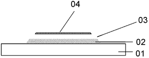
- FIG. 1(a) to 1(c) are flow charts of preparing an oxide thin film transistor using a back channel etching process according to a technique.
- the preparation of an oxide thin film transistor by a back channel etching process requires three masks to be completed by three patterning processes. That is, the gate 02 is formed by the first patterning process using the first mask (as shown in FIG. 1(a)); the gate insulating layer 03 is formed (as shown in FIG. 1(b)); The template forms the active layer 04 through the second patterning process (as shown in FIG. 1(b)); the source electrode 05 and the drain electrode 06 are formed by the third patterning process using the third mask (FIG. 1(c) Shown).
- the oxide thin film transistor can be simplified. Preparation process to reduce preparation costs.
- a method of fabricating an oxide thin film transistor includes forming a gate electrode, a gate insulating layer, an active layer, a source electrode, and a drain electrode.
- Forming the active layer, the source electrode, and the drain electrode includes: sequentially forming an oxide semiconductor film and a source/drain electrode metal film on the substrate, the entire surface of the oxide semiconductor film and the source leakage
- the epipolar metal film is in direct contact; and the oxide semiconductor film and the source/drain electrode metal film are patterned using a two-tone mask to form the active layer, the source electrode, and the drain electrode by one patterning process.
- the patterning the oxide semiconductor film and the source/drain electrode metal film with a two-tone mask to form an active layer, a source electrode, and a drain electrode by one patterning process include: a metal film at the source/drain electrode Forming a photoresist layer thereon; exposing and developing the photoresist layer to form a photoresist completely reserved portion, a photoresist portion remaining portion, and a photoresist completely removed portion, wherein the photoresist completely remains portion Corresponding to a region where the source electrode and the drain electrode are to be formed, the photoresist portion remaining portion corresponds to a region between the source electrode and the drain electrode where a channel is to be formed, the photoresist portion The thickness of the photoresist in the reserved region is smaller than the thickness of the photoresist in the completely remaining portion of the photoresist, and the completely removed region of the photoresist corresponds to other regions; the first etching process is performed to remove the photoresist Completely removing the source
- the source/drain electrode metal film is formed of Cu or a Cu alloy, and the second etching process uses a fluorine-free etchant.
- the Cu alloy is a CuMo alloy, a CuMn alloy, a CuTa alloy, a CuCa alloy, a CuMg alloy, or a CuMgAl alloy.
- the fluorine-free etching liquid is a fluorine-free H 2 O 2 -based etching liquid.
- the method further includes forming a first anti-oxidation cap layer covering the source electrode and a second anti-oxidation cap layer covering the drain electrode.
- Forming the active layer, the source electrode, the drain electrode, The first oxidation resistant cap layer and the second oxidation resistant cap layer include: sequentially forming an oxide semiconductor film, a source/drain electrode metal film, and an oxidation resistant film on the base substrate; and adopting the two-tone mask Patterning the oxide semiconductor film, the source/drain electrode metal film, and the oxidation resistant film to form the active layer, the source electrode, the drain electrode, and the first anti-etching by a patterning process An oxide cap layer and the second oxidation resistant cap layer.
- the patterning the oxide semiconductor film, the source/drain electrode metal film, and the oxidation resistant film with the two-tone mask to form the active layer, the source electrode, and the source electrode by a patterning process comprises: forming a photoresist layer on the anti-oxidation film, exposing and developing the photoresist layer to form a photoresist completely remaining portion, a photoresist portion remaining portion, and a photoresist completely removed portion, wherein the photoresist completely remaining portion corresponds to a region where the source electrode and the drain electrode are to be formed, the photolithography
- the glue portion remaining portion corresponds to a region between the source electrode and the drain electrode where a channel is to be formed, and a photoresist of the photoresist portion remaining region has a thickness smaller than that of the photoresist completely retained portion a thickness of the glue, the photoresist completely removed region corresponds to other regions; performing a first
- the source/drain electrode metal film is formed of Cu or a Cu alloy, and the third etching process uses a fluorine-free etchant.
- the Cu alloy is a CuMo alloy, a CuMn alloy, a CuTa alloy, a CuCa alloy, a CuMg alloy, or a CuMgAl alloy.
- the fluorine-free etching liquid is a fluorine-free H 2 O 2 -based etching liquid.
- the first etching process and the second etching process are wet etching processes, and an etching rate of the second etching process is smaller than an etching rate of the first etching process.
- the first oxidation resistant cap layer and the second oxidation resistant cap layer are formed of Mo or MoNb.
- the first anti-oxidation cap layer and the second anti-oxidation cap layer are made of an oxide semiconductor material form.
- the method further includes plasma treating the first anti-oxidation cap layer and/or the second anti-oxidation cap layer.
- the method further includes: forming a protective layer to cover the first anti-oxidation cap layer, the second anti-oxidation cap layer, the source electrode, the drain electrode, the active layer, the gate An insulating layer and the base substrate; and forming a first via hole in the protective layer to plasma treat the first oxidation resistant cap layer through the first via hole, and/or in the protection A second via is formed in the layer to plasma treat the second oxidation resistant cap layer through the second via.
- forming the first via in the protective layer, forming a second via in the protective layer, and performing the first anti-oxidation cap layer and/or the second anti-oxidation cap layer Plasma treatment is carried out in the same dry etching apparatus.
- the atmosphere in which the plasma treatment is performed is selected from one or more of He, SF 6 and H 2 .
- the first oxidation resistant cap layer, the second oxidation resistant cap layer, and the active layer are formed of the same material.
- the pattern of the first oxidation resistant cap layer is the same as the pattern of the source electrode, and the pattern of the second oxidation resistant cap layer is the same as the pattern of the drain electrode.
- 1(a) to 1(c) are flow diagrams of preparing an oxide thin film transistor using a back channel etching process according to a technique
- 2(a) to 2(g) illustrate a method of fabricating an oxide thin film transistor according to an embodiment of the present invention
- 3(a) to 3(g) illustrate variations of a method of fabricating an oxide thin film transistor according to an embodiment of the present invention
- 4(a) and 4(b) illustrate a method of fabricating an array substrate in accordance with an embodiment of the present invention.
- Embodiments of the present invention provide a method of fabricating an oxide thin film transistor.
- the method includes: forming a gate electrode, a gate insulating layer, an active layer, a source electrode, and a drain electrode, wherein forming the active layer, the source electrode, and the drain electrode comprises: sequentially forming an oxide on the substrate substrate a semiconductor film and a source/drain electrode metal film, the entire surface of the oxide semiconductor film is in direct contact with the source/drain electrode metal film; and the oxide semiconductor film and the source/drain electrode metal are patterned using a two-tone mask
- the thin film forms the active layer, the source electrode, and the drain electrode by one patterning process.
- the method of fabricating an oxide thin film transistor according to an embodiment of the present invention since the entire surface of the oxide semiconductor film is in direct contact with the source/drain electrode metal film, a back channel etching process may be employed to avoid preparation of an etch barrier. Floor. Further, in the method of fabricating an oxide thin film transistor according to an embodiment of the present invention, since a two-tone mask is employed, the active layer, the source electrode, and the drain electrode may be simultaneously formed by one patterning process Thus, the fabrication of the thin film transistor can be completed with only two masks.
- the method of fabricating an oxide thin film transistor according to an embodiment of the present invention organically combines a back channel etching process and a two-tone mask process, and can further reduce the number of masks while avoiding the formation of an etch barrier layer. This simplifies the manufacturing process, reduces production costs, and improves product yield.
- an oxide thin film transistor according to an embodiment of the present invention will be described with reference to the accompanying drawings Carry out a detailed description. It should be noted that the method for fabricating an oxide thin film transistor according to an embodiment of the present invention can be used for preparing a bottom gate type oxide thin film transistor, a top gate type oxide thin film transistor, or other types of oxide thin film transistors, and the bottom is only bottom.
- a gate oxide thin film transistor is described as an example.
- FIGS. 2(a) to 2(g) illustrate a method of fabricating an oxide thin film transistor according to an embodiment of the present invention.
- a method of manufacturing a thin film transistor according to an embodiment of the present invention includes the following steps.
- Step S1 forming a gate electrode
- a gate metal thin film 20 is formed on the base substrate 10, and the gate metal thin film 20 is patterned by a single-tone mask to form the gate electrode 21.
- the base substrate 10 may be a glass substrate, a quartz substrate, an organic substrate, or the like.
- the gate metal thin film 20 may be formed of an alloy such as Cr, W, Cu, Ti, Ta, Mo, Al, or the like.
- the gate metal film 20 is formed of, for example, a low-resistivity Cu or Cu alloy.
- the Cu alloy is a CuMo alloy, a CuMn alloy, a CuTa alloy, a CuCa alloy, a CuMg alloy, a CuMgAl alloy, or the like.
- the process of patterning the gate metal film 20 with a single-tone mask to form the gate electrode 21 is a conventional patterning process, which will not be described herein.
- Step S2 forming a gate insulating layer
- a gate insulating layer 30 is formed to cover the gate electrode 21 and the base substrate 10.
- the gate insulating layer 30 is formed of silicon nitride, silicon oxide, silicon oxynitride, aluminum oxide, or the like by plasma enhanced chemical vapor deposition, sputtering, or the like.
- Step S3 forming an active layer, a source electrode, and a drain electrode
- an oxide semiconductor film 40 and a source/drain electrode metal film 50 are sequentially formed on the gate insulating layer 30, the entire surface of the oxide semiconductor film 40 and the The source/drain electrode metal film 50 is in direct contact; and the oxide semiconductor film 40 and the source/drain electrode metal film 50 are patterned using a two-tone mask to form the active layer 41, the source electrode 51, and the drain electrode by one patterning process 52.
- the oxide semiconductor thin film 40 may be a thin film composed of at least two elements of an oxygen element and an element such as In (indium), Ga (gallium), Zn (zinc), or Sn (tin).
- the oxide semiconductor thin film 40 may be an IGZO (indium gallium zinc oxide) thin film, an IZO (indium zinc oxide) thin film, an InSnO (indium tin oxide) thin film, an InGaSnO (indium gallium oxide) thin film, or the like.
- the thickness of the oxide semiconductor film 40 is to Preferred to
- the source/drain electrode metal thin film 50 may be formed of a metal such as Cr, W, Cu, Ti, Ta, Mo, Al, or an alloy such as aluminum lanthanum.
- the source/drain electrode metal film 50 is formed of, for example, a low-resistivity Cu or Cu alloy.
- the Cu alloy is a CuMo alloy, a CuMn alloy, a CuTa alloy, a CuCa alloy, a CuMg alloy, a CuMgAl alloy, or the like.
- the two-tone mask is a halftone mask or a gray tone mask.
- the patterning of the oxide semiconductor film 40 and the source/drain metal film 50 by a two-tone mask to form the active layer 41, the source electrode 51 and the drain electrode 52 by one patterning process include:
- the thickness of the photoresist is smaller than the thickness of the photoresist in the completely remaining portion of the photoresist, and the photoresist completely removed region corresponds to other regions, as shown in FIG. 2(d);
- the source/drain electrode metal film 50 is formed of, for example, a low-resistivity Cu or Cu alloy.
- a display device such as a liquid crystal display device, an organic light emitting display device, or the like, by patterning the source/drain electrode metal film 50, a data line directly connected or integrally formed with the source electrode 51 may be simultaneously and in the same layer as the source electrode 51 and the drain electrode 52.
- the source/drain electrode metal film 50 is made of low resistivity Cu or When the Cu alloy is formed, the data line, the source electrode 51, and the drain electrode 52 excellent in conductivity can be simultaneously obtained, which is very advantageous for a large-sized display device.
- the second etching process is performed, for example, by using a fluorine-free etching solution to remove the source leakage of the photoresist portion remaining region.
- An epipolar metal film 50 is formed to form the source electrode 51 and the drain electrode 50. The inventors have found that the source-drain electrode metal film 50 of the remaining portion of the photoresist portion can be sufficiently etched by using a fluorine-free etchant, and damage to the active layer 41 can be effectively reduced or even avoided.
- the fluorine-free etching liquid is a fluorine-free H 2 O 2 -based etching liquid; the fluorine-free H 2 O 2 -based etching liquid is an etching liquid containing no fluorine-containing H 2 O 2 as a main component, for example, in the etching liquid.
- the proportion of fluorine-free H 2 O 2 is about 5% to 30%.
- the fluorine-free H 2 O 2 -based etching liquid is a neutral fluorine-free H 2 O 2 etching liquid.
- the first etching process described above is a wet etching process and, for example, an acid etching solution is used.
- the method of fabricating the oxide thin film transistor according to the embodiment of the present invention can be completed by the above steps S1, S2 and S3.
- the method of fabricating an oxide thin film transistor according to an embodiment of the present invention does not require the preparation of an etch barrier layer, which organically combines a back channel etch process and a two-tone mask process, and can further reduce the formation of an etch barrier while avoiding The number of reticle simplifies the manufacturing process, reduces manufacturing costs, and improves product yield.
- a method for preparing an oxide thin film transistor according to an embodiment of the present invention uses a Cu or a Cu alloy to form a source/drain electrode metal film, thereby obtaining a source electrode and a drain electrode having excellent conductivity characteristics, which is advantageous for an oxide thin film transistor.
- the method for fabricating a thin film transistor uses a fluorine-free etching solution to etch and remove a source/drain electrode metal film of a portion of the photoresist remaining portion, which can sufficiently etch and remove the source and drain of the remaining portion of the photoresist portion.
- the ultra-metal thin film can effectively reduce or even avoid damage to the active layer and improve the characteristics of the oxide thin film transistor.
- the oxide thin film transistor In order to further improve the characteristics of the oxide thin film transistor, it is generally required to anneal the oxide thin film transistor a plurality of times or form a protective layer such as SiO 2 on the oxide thin film transistor.
- a protective layer such as SiO 2
- the source electrode 51 and the drain electrode 52 may be more or less oxidized, and the source electrode 51 and the drain electrode 52 are made of a low-resistivity Cu or Cu alloy. Oxidation is more pronounced in the case of formation.
- the method of fabricating a thin film transistor according to an embodiment of the present invention further includes: forming a first oxidation resistant cap layer 61 covering the source electrode 51 and a second oxidation resistant cap layer 62 covering the drain electrode 52. .
- a first oxidation resistant cap layer 61 covering the source electrode 51 and a second oxidation resistant cap layer 62 covering the drain electrode 52.
- 3(a) to 3(g) show a modification of a method of manufacturing an oxide thin film transistor in which a first oxidation resistant cap layer 61 and a second oxidation resistant cap layer 62 are formed, according to an embodiment of the present invention.
- a modification of the method of manufacturing an oxide thin film transistor according to an embodiment of the present invention includes the following steps.
- Step S11 forming a gate electrode
- step is the same as the above step S1, and reference may be made to FIG. 2(a) and FIG. 2(b), and details are not described herein again.
- Step S22 forming a gate insulating layer
- this step is the same as step S2 above, and can be seen in FIG. 2(c), and details are not described herein again.
- Step S33 forming an active layer, a source electrode, a drain electrode, a first oxidation resistant cap layer, and a second oxidation resistant cap layer.
- an oxide semiconductor film 40, a source/drain electrode metal film 50, and an oxidation resistant film 60 are sequentially formed on the gate insulating layer 30; and the two-tone mask is employed.
- the template is patterned to form the oxide semiconductor film 40, the source/drain electrode metal film 50, and the oxidation resistant film 60 to form the active layer 41, the source electrode 51, and the drain electrode 52 by one patterning process.
- the two-tone mask is a halftone mask or a gray tone mask.
- the oxide semiconductor film 40, the source/drain electrode metal film 50, and the oxidation resistant film 60 are patterned by using the two-tone mask to form the active layer 41 by a patterning process.
- the source electrode 51, the drain electrode 52, the first oxidation resistant cap layer 61 and the second oxidation resistant cap layer 62 comprise:
- the thickness of the photoresist is smaller than the thickness of the photoresist in the completely remaining portion of the photoresist, and the photoresist completely removed region corresponds to other regions, as shown in FIG. 3(b);
- the photoresist of the completely remaining portion of the photoresist is removed as shown in FIG. 3(f).
- the source/drain electrode metal film 50 can be formed of a low-resistivity Cu or Cu alloy, whereby source and drain electrodes excellent in conductivity characteristics can be obtained, which is advantageous for application of an oxide thin film transistor to a large-sized display. Device.
- the third etching process uses, for example, a fluorine-free etching solution to etch away the source of the photoresist portion remaining region. The electrode metal film 50 is drained to form the source electrode 51 and the drain electrode 50.
- the fluorine-free etching liquid is a fluorine-free H 2 O 2 -based etching liquid; the fluorine-free H 2 O 2 -based etching liquid is an etching liquid containing no fluorine-containing H 2 O 2 as a main component, for example, in the etching liquid.
- the proportion of fluorine-free H 2 O 2 is about 5% to 30%.
- the fluorine-free H 2 O 2 -based etching liquid is a neutral fluorine-free H 2 O 2 etching liquid.
- the first etching process and the second etching process in the above step S33 are both a wet etching process, and an acid-based etching liquid is used, for example.
- the etch rate of the second etch process is less than the etch rate of the first etch process.
- the oxidation resistant film 60, the source/drain metal film 50, and the oxide semiconductor film 40 in the completely removed region of the photoresist can be quickly and efficiently removed in the first etching process.
- the second etching process the oxidation resistant film 60 of the photoresist portion remaining region can be effectively removed while preventing the etching solution from penetrating the source/drain electrode metal film 50 located in the remaining portion of the photoresist portion.
- the active layer 41 is damaged, thereby balancing efficiency and quality.
- the process difficulty can be reduced and the process efficiency can be improved.
- step S33 since the second etching process and the third etching process both use the photoresist which is completely retained by the photoresist as a mask, the first anti-etch formed in the second etching process
- the pattern of the oxide cap layer 61 and the pattern of the second oxidation resistant cap layer 62 are respectively the same as those of the source electrode 51 and the drain electrode 52 formed in the third etching process.
- the first anti-oxidation cap layer 61 and the second anti-oxidation cap layer 62 have a thickness of to Preferred to
- the first oxidation resistant cap layer 61 and the second oxidation resistant cap layer 62 are formed of Mo, MoNb, or the like.
- the first oxidation resistant cap layer 61 and the second oxidation resistant cap layer 62 are formed of an oxide semiconductor material; in this case, the oxidation resistant film 60 is an oxide semiconductor film.
- the oxidation-resistant film 60 is an oxide semiconductor film, the following advantageous effects can be obtained: (1) the adhesion of the oxide semiconductor film to the photoresist is good, and the first, second, and third etchings are performed as described above. The glue phenomenon does not occur in the process; (2) the galvanic effect between the oxide semiconductor film and the source/drain electrode metal film 50 (for example, formed of Cu or Cu alloy) is small, and a good etching slope angle is easily formed. Conducive to the subsequent process.
- the oxide semiconductor material forming the first oxidation resistant cap layer 61 and the second oxidation resistant cap layer 62 may be composed of oxygen and In (indium), Ga (gallium), Zn (zinc), Sn ( At least two elements of elements such as tin).
- the oxide semiconductor material may be IGZO, IZO, InSnO, InGaSnO, or the like.
- the oxidation resistant film 60 is an oxide semiconductor film, and the inventors of the present invention found The amount of oxygen introduced when the oxide semiconductor film is prepared is extremely small, and has little influence on the source/drain electrode metal film 50.
- a modification of the method of manufacturing an oxide thin film transistor according to an embodiment of the present invention further includes: The first anti-oxidation cap layer 61 and/or the second anti-oxidation cap layer 62 are subjected to plasma treatment. In this way, the first anti-oxidation cap layer 61 and/or the second anti-oxidation cap layer 62 can be converted from a semiconductor to a conductor, facilitating electrical connection between the source electrode 51 and/or the drain electrode 52 and the external line.
- both of the second oxidation resistant cap layers 62 are plasma treated.
- the source electrode 51 and the data line are generally Directly connected or integrally formed, the first anti-oxidation cap layer 61 covering the source electrode 51 may not be subjected to plasma treatment.
- a modification of the method of fabricating a thin film transistor according to an embodiment of the present invention further includes: forming a protective layer 70 to cover the first anti-oxidation cap layer 61, the second anti-oxidation cap a layer 62, the source electrode 51, the drain electrode 52, the active layer 41, the gate insulating layer 30, and the base substrate 10; and forming a first via 71 in the protective layer 70
- the first anti-oxidation cap layer 61 is plasma-treated through the first via 71, and/or a second via 72 is formed in the protective layer 70 to pass through the second via 72
- the second anti-oxidation cap layer 62 is subjected to plasma treatment.
- the protective layer 70 may protect the thin film transistor from the external environment, and the protective layer 70 is formed of silicon oxide, silicon nitride, or silicon oxynitride.
- the first via 71 is formed in the protective layer 70
- the second via 72 is formed in the protective layer 70
- the oxidation resistant cap layer 62 is subjected to plasma treatment in the same dry etching apparatus. Thereby, the process difficulty can be simplified and the process efficiency can be improved.
- the atmosphere for plasma treatment of the first oxidation resistant cap layer 61 and/or the second oxidation resistant cap layer 62 is selected from one or more of He, SF 6 and H 2 .
- the first oxidation resistant cap layer 61 and the second oxidation resistant cap layer 62 may be formed of an oxide semiconductor material, and the active layer 41 is obtained by patterning the oxide semiconductor film 40. It can thus be seen that the first anti-oxidation cap layer 61, the second anti-oxidation cap layer 62 and the active layer 41 can be formed of the same material, such as IGZO. As a result, equipment investment and raw material types can be reduced, and process costs can be reduced. In consideration of the respective functions of the active layer 41 and the oxidation resistant cap layers 61 and 62, for example, the thickness of the active layer 41 is smaller than the thickness of the oxidation resistant cap layers 61 and 62.
- the oxidation resistant film 60 formed of IGZO and the oxide semiconductor thin film 40 formed of IGZO sandwich a source/drain electrode metal film 50 formed of Cu or a Cu alloy therebetween, thereby passing through the above-described step S33
- the patterning process can obtain the first anti-oxidation cap layer 61 and the second anti-oxidation cap layer 62 formed of IGZO, the source electrode 51 and the drain electrode 52 formed of Cu or a Cu alloy, and the active layer 41 formed of IGZO. .
- a modification of the method of manufacturing an oxide thin film transistor according to an embodiment of the present invention can obtain the same technical effects as the method of manufacturing an oxide thin film transistor according to an embodiment of the present invention as described above.
- a first anti-oxidation cap layer covering the source electrode and a second anti-oxidation cap layer covering the drain electrode are formed, It is possible to prevent the source electrode and the drain electrode from being oxidized.
- the method of fabricating the oxide thin film transistor according to the embodiment of the present invention can be well compatible with the method of fabricating the array substrate of the display device.
- the display device may be any product or component having a display function such as a liquid crystal panel, an organic light emitting display panel, a mobile phone, a tablet computer, a television, a display, a notebook computer, a digital photo frame, a navigator, or the like.
- an embodiment of the present invention further provides a method of fabricating an array substrate.
- the array substrate includes a display area and a peripheral area surrounding the display area.
- a plurality of gate lines and a plurality of data lines cross each other to form a plurality of sub-pixels arranged in a matrix, and pixel electrodes and pixels are formed in each sub-pixel.
- Electrode-connected thin film transistor is a method of fabricating an array substrate.
- a method of fabricating an array substrate according to an embodiment of the present invention includes the following steps.
- Step S111 forming a gate, a gate line, and a gate pad
- the gate metal film 20 is patterned using a single-tone mask to simultaneously form the gate electrode 21, the gate line (not shown), and the gate pad 22 .
- This step S111 differs from the above-described steps S1 and S11 in that the pattern of the single-tone mask is changed.
- the gate line is connected to the gate electrode 21, and the gate line pad 22 is located in a peripheral region of the array substrate, and the gate line pad 22 is connected to the gate line to connect the gate line to the driving circuit.
- Step S222 forming a gate insulating layer
- a gate insulating layer 30 is formed to cover the gate electrode 21, the gate line, the gate line pad 22, and the base substrate 10.
- Step S333 forming an active layer, a source electrode, a drain electrode, a data line, and a data line pad.
- the oxide semiconductor film 40 and the source/drain electrode metal film 50 are patterned using a two-tone mask to form the active layer 41 and the source electrode by one patterning process. 51.
- the step S333 differs from the above step S3 in that the pattern of the two-tone mask is changed such that the photoresist completely remains corresponding to the region where the source and drain electrodes are to be formed, the region where the data line is to be formed, and The area where the data line pads are formed.
- the data line is connected to the source electrode 51, and the data line pad 90 is located in the peripheral area of the array substrate, and the data line pad 90 is connected to the data line to connect the data line to the driving circuit.
- the data line pad 90 has a two-layer structure including a semiconductor layer 42.
- the metal layer 53, the semiconductor layer 42 is formed in the same layer and the same material as the active layer 41, and the metal layer 53 is formed in the same layer and the same material as the source electrode 51 and the drain electrode 52.
- the data line is also a two-layer structure, one layer is formed in the same layer as the active layer 41, and the other layer is formed in the same layer as the source electrode 51 and the drain electrode 52.
- the first anti-oxidation cap layer 61 and the second anti-oxidation cap layer may also be formed in this step S333.
- the oxide semiconductor film 40, the source/drain electrode metal film 50, and the oxidation resistant film are patterned using a two-tone mask to form an active layer by one patterning process. 41.
- the data line pad 90 has a three-layer structure including a semiconductor layer 42, a metal layer 53, and an oxidation resistant layer 63.
- the semiconductor layer 42 is in the same layer as the active layer 41. The material is formed.
- the metal layer 53 is formed in the same layer and the same material as the source electrode 51 and the drain electrode 52.
- the oxidation resistant layer 63 is formed in the same layer and the same material as the first oxidation resistant cap layer 61 and the second oxidation resistant cap layer 62.
- the data line is also a three-layer structure, one layer is formed in the same layer as the active layer 41, and the same layer is formed in the same layer as the source electrode 51 and the drain electrode 52, and the first layer is formed with the same material.
- the oxide cap layer 61 and the second oxidation resistant cap layer 62 are formed in the same layer and in the same material.
- Step S444 forming a protective layer and via holes
- a protective layer 70 is formed, and the protective layer 70 is patterned to form a second via 72, a third via 73, and a fourth via 74.
- the second via 72 exposes the drain electrode 52
- the third via 73 exposes the gate pad 22
- the fourth via 74 exposes the data line pad 74.
- Step S555 forming a pixel electrode
- a pixel electrode 80 is formed, which is connected to the drain electrode 52 through the second via 72.
- the pixel electrode 80 is formed of a transparent conductive material such as ITO.
- the method for fabricating the array substrate according to the embodiment of the present invention may further include: performing plasma treatment on the second oxidation resistant cap layer 62 through the second via hole 72.
- the oxidation resistant layer 63 in the data line pad 90 can also be plasma treated. Specific details of the plasma treatment can be referred to the above description, and will not be described herein.
- the system for fabricating an array substrate according to an embodiment of the present invention can be completed by the above steps S111 to S555.
- Preparation method A method of fabricating an array substrate according to an embodiment of the present invention is based on a method of fabricating an oxide thin film transistor according to an embodiment of the present invention, and thus the same technical effects as those of an oxide thin film transistor according to an embodiment of the present invention can be obtained. I will not repeat them here.
Landscapes
- Engineering & Computer Science (AREA)
- Power Engineering (AREA)
- Microelectronics & Electronic Packaging (AREA)
- Computer Hardware Design (AREA)
- General Physics & Mathematics (AREA)
- Condensed Matter Physics & Semiconductors (AREA)
- Physics & Mathematics (AREA)
- Ceramic Engineering (AREA)
- Manufacturing & Machinery (AREA)
- Chemical & Material Sciences (AREA)
- Crystallography & Structural Chemistry (AREA)
- Thin Film Transistor (AREA)
- Electrodes Of Semiconductors (AREA)
Abstract
Description
Claims (19)
- 一种氧化物薄膜晶体管的制备方法,包括:形成栅极、栅绝缘层、有源层、源电极和漏电极,其中形成所述有源层、所述源电极和所述漏电极包括:在衬底基板上依次形成氧化物半导体薄膜和源漏电极金属薄膜,所述氧化物半导体薄膜的整个表面与所述源漏电极金属薄膜直接接触;以及采用双色调掩模板图案化所述氧化物半导体薄膜和所述源漏电极金属薄膜以通过一次构图工艺形成所述有源层、所述源电极和所述漏电极。
- 根据权利要求1所述的氧化物薄膜晶体管的制备方法,其中所述采用双色调掩模板图案化所述氧化物半导体薄膜和所述源漏电极金属薄膜以通过一次构图工艺形成有源层、源电极和漏电极包括:在所述源漏电极金属薄膜上形成光刻胶层;对所述光刻胶层进行曝光、显影以形成光刻胶完全保留部分、光刻胶部分保留部分和光刻胶完全去除部分,其中所述光刻胶完全保留部分对应于要形成所述源电极和所述漏电极的区域,所述光刻胶部分保留部分对应于所述源电极和所述漏电极之间要形成沟道的区域,所述光刻胶部分保留区域的光刻胶的厚度小于所述光刻胶完全保留部分的光刻胶的厚度,所述光刻胶完全去除区域对应于其他区域;进行第一次蚀刻工艺,去除所述光刻胶完全去除区域的所述源漏金属薄膜和所述氧化物半导体薄膜,以形成所述有源层;进行灰化工艺,去除所述光刻胶部分保留区域的光刻胶;进行第二次蚀刻工艺,去除所述光刻胶部分保留区域的所述源漏电极金属薄膜,以形成所述源电极和所述漏电极;以及去除所述光刻胶完全保留部分的光刻胶。
- 根据权利要求2所述的氧化物薄膜晶体管的制备方法,其中所述源漏电极金属薄膜由Cu或Cu合金形成,且所述第二次蚀刻工艺采用无氟蚀刻液。
- 根据权利要求3所述的氧化物薄膜晶体管的制备方法,其中所述Cu合金为CuMo合金、CuMn合金、CuTa合金、CuCa合金、CuMg合金或CuMgAl合金。
- 根据权利要求3所述的氧化物薄膜晶体管的制备方法,其中所述无氟蚀刻液为无氟H2O2系蚀刻液。
- 根据权利要求1所述的氧化物薄膜晶体管的制备方法,还包括:形成覆盖所述源电极的第一抗氧化盖层和覆盖所述漏电极的第二抗氧化盖层,其中形成所述有源层、所述源电极、所述漏电极、所述第一抗氧化盖层和所述第二抗氧化盖层包括:在所述衬底基板上依次形成氧化物半导体薄膜、源漏电极金属薄膜和抗氧化薄膜;以及采用所述双色调掩模板图案化所述氧化物半导体薄膜、所述源漏电极金属薄膜和所述抗氧化薄膜以通过一次构图工艺形成所述有源层、所述源电极、所述漏电极、所述第一抗氧化盖层和所述第二抗氧化盖层。
- 根据权利要求6所述的氧化物薄膜晶体管的制备方法,其中所述采用所述双色调掩模板图案化所述氧化物半导体薄膜、所述源漏电极金属薄膜和所述抗氧化薄膜以通过一次构图工艺形成所述有源层、所述源电极、所述漏电极、所述第一抗氧化盖层和所述第二抗氧化盖层包括:在所述抗氧化薄膜上形成光刻胶层,对所述光刻胶层进行曝光、显影以形成光刻胶完全保留部分、光刻胶部分保留部分和光刻胶完全去除部分,其中所述光刻胶完全保留部分对应于要形成所述源电极和所述漏电极的区域,所述光刻胶部分保留部分对应于所述源电极和所述漏电极之间要形成沟道的区域,所述光刻胶部分保留区域的光刻胶的厚度小于所述光刻胶完全保留部分的光刻胶的厚度,所述光刻胶完全去除区域对应于其他区域;进行第一次蚀刻工艺,去除所述光刻胶完全去除区域的所述抗氧化薄膜、所述源漏金属薄膜和所述氧化物半导体薄膜,以形成所述有源层;进行灰化工艺,去除所述光刻胶部分保留区域的光刻胶;进行第二次蚀刻工艺,去除所述光刻胶部分保留区域的所述抗氧化薄膜,以形成所述第一抗氧化盖层和所述第二抗氧化盖层;进行第三次蚀刻工艺,去除所述光刻胶部分保留区域的所述源漏电极金属薄膜,以形成所述源电极和所述漏电极;以及去除所述光刻胶完全保留部分的光刻胶。
- 根据权利要求7所述的氧化物薄膜晶体管的制备方法,其中所述源漏 电极金属薄膜由Cu或Cu合金形成,且所述第三次蚀刻工艺采用无氟蚀刻液。
- 根据权利要求8所述的氧化物薄膜晶体管的制备方法,其中所述Cu合金为CuMo合金、CuMn合金、CuTa合金、CuCa合金、CuMg合金或CuMgAl合金。
- 根据权利要求8所述的氧化物薄膜晶体管的制备方法,其中所述无氟蚀刻液为无氟H2O2系蚀刻液。
- 根据权利要求7所述的氧化物薄膜晶体管的制备方法,其中所述第一次蚀刻工艺和所述第二次蚀刻工艺为湿法蚀刻工艺,且所述第二次蚀刻工艺的蚀刻速率小于所述第一次蚀刻工艺的蚀刻速率。
- 根据权利要求6所述的氧化物薄膜晶体管的制备方法,其中所述第一抗氧化盖层和所述第二抗氧化盖层由Mo或MoNb形成。
- 根据权利要求6所述的氧化物薄膜晶体管的制备方法,其中所述第一抗氧化盖层和所述第二抗氧化盖层由氧化物半导体材料形成。
- 根据权利要求13所述的氧化物薄膜晶体管的制备方法,还包括:对所述第一抗氧化盖层和/或所述第二抗氧化盖层进行等离子体处理。
- 根据权利要求14所述的氧化物薄膜晶体管的制备方法,还包括:形成保护层以覆盖所述第一抗氧化盖层、所述第二抗氧化盖层、所述源电极、所述漏电极、所述有源层、所述栅绝缘层和所述衬底基板;以及在所述保护层中形成第一过孔以通过所述第一过孔对所述第一抗氧化盖层进行等离子体处理,和/或在所述保护层中形成第二过孔以通过所述第二过孔对所述第二抗氧化盖层进行等离子体处理。
- 根据权利要求15所述的氧化物薄膜晶体管的制备方法,其中在所述保护层中形成所述第一过孔、在所述保护层中形成第二过孔、以及对所述第一抗氧化盖层和/或所述第二抗氧化盖层进行等离子体处理在同一干刻设备中进行。
- 根据权利要求14所述的氧化物薄膜晶体管的制备方法,其中进行所述等离子处理的气氛选自He、SF6和H2中的一种或几种。
- 根据权利要求13-17任一项所述的氧化物薄膜晶体管的制备方法,其中所述第一抗氧化盖层、所述第二抗氧化盖层和所述有源层由相同的材料形成。
- 根据权利要求6-17任一项所述的氧化物薄膜晶体管的制备方法,其中所述第一抗氧化盖层的图案与所述源电极的图案相同,并且所述第二抗氧化盖层的图案与所述漏电极的图案相同。
Priority Applications (1)
| Application Number | Priority Date | Filing Date | Title |
|---|---|---|---|
| US15/308,991 US9812472B2 (en) | 2015-07-15 | 2016-01-25 | Preparation method of oxide thin-film transistor |
Applications Claiming Priority (2)
| Application Number | Priority Date | Filing Date | Title |
|---|---|---|---|
| CN201510415622.5A CN105140131A (zh) | 2015-07-15 | 2015-07-15 | 氧化物薄膜晶体管的制备方法 |
| CN201510415622.5 | 2015-07-15 |
Publications (1)
| Publication Number | Publication Date |
|---|---|
| WO2017008497A1 true WO2017008497A1 (zh) | 2017-01-19 |
Family
ID=54725437
Family Applications (1)
| Application Number | Title | Priority Date | Filing Date |
|---|---|---|---|
| PCT/CN2016/072012 WO2017008497A1 (zh) | 2015-07-15 | 2016-01-25 | 氧化物薄膜晶体管的制备方法 |
Country Status (3)
| Country | Link |
|---|---|
| US (1) | US9812472B2 (zh) |
| CN (1) | CN105140131A (zh) |
| WO (1) | WO2017008497A1 (zh) |
Families Citing this family (11)
| Publication number | Priority date | Publication date | Assignee | Title |
|---|---|---|---|---|
| CN105140131A (zh) * | 2015-07-15 | 2015-12-09 | 京东方科技集团股份有限公司 | 氧化物薄膜晶体管的制备方法 |
| CN107093583A (zh) * | 2017-05-03 | 2017-08-25 | 京东方科技集团股份有限公司 | 一种阵列基板及其制备方法、显示装置 |
| CN107768307A (zh) * | 2017-11-21 | 2018-03-06 | 深圳市华星光电半导体显示技术有限公司 | 背沟道蚀刻型tft基板及其制作方法 |
| CN108183132A (zh) | 2017-12-27 | 2018-06-19 | 深圳市华星光电半导体显示技术有限公司 | 一种igzo薄膜晶体管制备方法 |
| CN108550626A (zh) * | 2018-04-18 | 2018-09-18 | 深圳市华星光电技术有限公司 | 薄膜晶体管器件的制作方法和薄膜晶体管器件 |
| CN109192704A (zh) * | 2018-09-05 | 2019-01-11 | 京东方科技集团股份有限公司 | 阵列基板及其制造方法、显示装置 |
| CN110676265B (zh) * | 2019-09-25 | 2022-02-08 | 南京京东方显示技术有限公司 | 一种显示面板的制造方法 |
| CN110798916B (zh) * | 2019-11-19 | 2023-04-11 | 京东方科技集团股份有限公司 | 一种加热器及其制备方法、传感器、智能终端 |
| CN111472000B (zh) * | 2020-04-15 | 2021-07-27 | 苏州华星光电技术有限公司 | 一种铜钼膜层的蚀刻方法、阵列基板 |
| CN113594181A (zh) * | 2021-07-23 | 2021-11-02 | 惠州华星光电显示有限公司 | 阵列基板及其制备方法 |
| CN113764282B (zh) * | 2021-09-03 | 2023-09-05 | 深圳市华星光电半导体显示技术有限公司 | 一种背沟道蚀刻型的薄膜电晶体及其制作方法 |
Citations (6)
| Publication number | Priority date | Publication date | Assignee | Title |
|---|---|---|---|---|
| WO2004055917A2 (en) * | 2002-12-14 | 2004-07-01 | Koninklijke Philips Electronics N.V. | Manufacture of thin film transistors |
| US20060183263A1 (en) * | 2005-02-16 | 2006-08-17 | Chin-Mao Lin | Structure and Manufacturing Method of An Image TFT Array |
| CN101097381A (zh) * | 2006-06-30 | 2008-01-02 | Lg.菲利浦Lcd株式会社 | 液晶显示器件的制造方法 |
| CN102812555A (zh) * | 2010-03-11 | 2012-12-05 | 夏普株式会社 | 半导体装置及其制造方法 |
| CN103715272A (zh) * | 2014-01-16 | 2014-04-09 | 广州新视界光电科技有限公司 | 金属氧化物薄膜晶体管及其制备方法 |
| CN105140131A (zh) * | 2015-07-15 | 2015-12-09 | 京东方科技集团股份有限公司 | 氧化物薄膜晶体管的制备方法 |
Family Cites Families (4)
| Publication number | Priority date | Publication date | Assignee | Title |
|---|---|---|---|---|
| CN102237305B (zh) * | 2010-05-06 | 2013-10-16 | 北京京东方光电科技有限公司 | 阵列基板及其制造方法和液晶显示器 |
| KR20120138074A (ko) * | 2011-06-14 | 2012-12-24 | 삼성디스플레이 주식회사 | 박막 트랜지스터, 및 박막 트랜지스터 표시판과 이들을 제조하는 방법 |
| US9365770B2 (en) * | 2011-07-26 | 2016-06-14 | Mitsubishi Gas Chemical Company, Inc. | Etching solution for copper/molybdenum-based multilayer thin film |
| CN103745955B (zh) * | 2014-01-03 | 2017-01-25 | 京东方科技集团股份有限公司 | 显示装置、阵列基板及其制造方法 |
-
2015
- 2015-07-15 CN CN201510415622.5A patent/CN105140131A/zh active Pending
-
2016
- 2016-01-25 WO PCT/CN2016/072012 patent/WO2017008497A1/zh active Application Filing
- 2016-01-25 US US15/308,991 patent/US9812472B2/en active Active
Patent Citations (6)
| Publication number | Priority date | Publication date | Assignee | Title |
|---|---|---|---|---|
| WO2004055917A2 (en) * | 2002-12-14 | 2004-07-01 | Koninklijke Philips Electronics N.V. | Manufacture of thin film transistors |
| US20060183263A1 (en) * | 2005-02-16 | 2006-08-17 | Chin-Mao Lin | Structure and Manufacturing Method of An Image TFT Array |
| CN101097381A (zh) * | 2006-06-30 | 2008-01-02 | Lg.菲利浦Lcd株式会社 | 液晶显示器件的制造方法 |
| CN102812555A (zh) * | 2010-03-11 | 2012-12-05 | 夏普株式会社 | 半导体装置及其制造方法 |
| CN103715272A (zh) * | 2014-01-16 | 2014-04-09 | 广州新视界光电科技有限公司 | 金属氧化物薄膜晶体管及其制备方法 |
| CN105140131A (zh) * | 2015-07-15 | 2015-12-09 | 京东方科技集团股份有限公司 | 氧化物薄膜晶体管的制备方法 |
Also Published As
| Publication number | Publication date |
|---|---|
| US20170162612A1 (en) | 2017-06-08 |
| US9812472B2 (en) | 2017-11-07 |
| CN105140131A (zh) | 2015-12-09 |
Similar Documents
| Publication | Publication Date | Title |
|---|---|---|
| WO2017008497A1 (zh) | 氧化物薄膜晶体管的制备方法 | |
| CN105161505B (zh) | 一种阵列基板及其制作方法、显示面板 | |
| US9455324B2 (en) | Thin film transistor and method of fabricating the same, array substrate and method of fabricating the same, and display device | |
| US20130175552A1 (en) | Array substrate and manufacturing method | |
| US9761616B2 (en) | Manufacturing method of array substrate with reduced number of patterning processes array substrate and display device | |
| WO2017219438A1 (zh) | Tft基板的制造方法 | |
| US10566458B2 (en) | Array substrate and method for manufacturing the same | |
| US11087985B2 (en) | Manufacturing method of TFT array substrate | |
| WO2016119324A1 (zh) | 阵列基板及其制作方法、显示装置 | |
| WO2013131380A1 (zh) | 阵列基板及其制作方法和显示装置 | |
| WO2015149482A1 (zh) | 阵列基板及其制作方法、显示装置 | |
| WO2019205440A1 (zh) | Tft基板的制作方法及tft基板 | |
| WO2018113214A1 (zh) | 薄膜晶体管及其制作方法、显示基板、显示装置 | |
| US9276014B2 (en) | Array substrate and method of fabricating the same, and liquid crystal display device | |
| WO2013127202A1 (zh) | 阵列基板的制造方法及阵列基板、显示器 | |
| US20160284741A1 (en) | Array substrate fabricating method | |
| WO2018205886A1 (zh) | 薄膜晶体管及其制作方法、阵列基板和显示装置 | |
| WO2017202115A1 (zh) | 薄膜晶体管及其制作方法、衬底基板及显示装置 | |
| WO2016026207A1 (zh) | 阵列基板及其制作方法和显示装置 | |
| WO2013181915A1 (zh) | Tft阵列基板及其制造方法和显示装置 | |
| WO2017028493A1 (zh) | 薄膜晶体管及其制作方法、显示器件 | |
| CN109037241B (zh) | Ltps阵列基板及其制造方法、显示面板 | |
| KR20160017867A (ko) | 표시장치와 그 제조 방법 | |
| TWI424507B (zh) | 薄膜電晶體陣列基板的製造方法 | |
| CN104681626A (zh) | 氧化物薄膜晶体管及其制作方法、阵列基板 |
Legal Events
| Date | Code | Title | Description |
|---|---|---|---|
| WWE | Wipo information: entry into national phase |
Ref document number: 15308991 Country of ref document: US |
|
| 121 | Ep: the epo has been informed by wipo that ep was designated in this application |
Ref document number: 16823645 Country of ref document: EP Kind code of ref document: A1 |
|
| NENP | Non-entry into the national phase |
Ref country code: DE |
|
| 122 | Ep: pct application non-entry in european phase |
Ref document number: 16823645 Country of ref document: EP Kind code of ref document: A1 |
|
| 32PN | Ep: public notification in the ep bulletin as address of the adressee cannot be established |
Free format text: NOTING OF LOSS OF RIGHTS PURSUANT TO RULE 112(1) EPC (EPO FORM 1205A DATED 22.08.2018) |