WO2016157611A1 - 露光データ生成方法、製造方法、露光データ生成装置、露光データ生成プログラム、および、製造システム - Google Patents
露光データ生成方法、製造方法、露光データ生成装置、露光データ生成プログラム、および、製造システム Download PDFInfo
- Publication number
- WO2016157611A1 WO2016157611A1 PCT/JP2015/083016 JP2015083016W WO2016157611A1 WO 2016157611 A1 WO2016157611 A1 WO 2016157611A1 JP 2015083016 W JP2015083016 W JP 2015083016W WO 2016157611 A1 WO2016157611 A1 WO 2016157611A1
- Authority
- WO
- WIPO (PCT)
- Prior art keywords
- exposure
- layer
- resist
- multilayer
- area
- Prior art date
- Legal status (The legal status is an assumption and is not a legal conclusion. Google has not performed a legal analysis and makes no representation as to the accuracy of the status listed.)
- Ceased
Links
Images














Classifications
-
- G—PHYSICS
- G03—PHOTOGRAPHY; CINEMATOGRAPHY; ANALOGOUS TECHNIQUES USING WAVES OTHER THAN OPTICAL WAVES; ELECTROGRAPHY; HOLOGRAPHY
- G03F—PHOTOMECHANICAL PRODUCTION OF TEXTURED OR PATTERNED SURFACES, e.g. FOR PRINTING, FOR PROCESSING OF SEMICONDUCTOR DEVICES; MATERIALS THEREFOR; ORIGINALS THEREFOR; APPARATUS SPECIALLY ADAPTED THEREFOR
- G03F7/00—Photomechanical, e.g. photolithographic, production of textured or patterned surfaces, e.g. printing surfaces; Materials therefor, e.g. comprising photoresists; Apparatus specially adapted therefor
- G03F7/70—Microphotolithographic exposure; Apparatus therefor
- G03F7/70483—Information management; Active and passive control; Testing; Wafer monitoring, e.g. pattern monitoring
- G03F7/70491—Information management, e.g. software; Active and passive control, e.g. details of controlling exposure processes or exposure tool monitoring processes
- G03F7/70508—Data handling in all parts of the microlithographic apparatus, e.g. handling pattern data for addressable masks or data transfer to or from different components within the exposure apparatus
-
- G—PHYSICS
- G03—PHOTOGRAPHY; CINEMATOGRAPHY; ANALOGOUS TECHNIQUES USING WAVES OTHER THAN OPTICAL WAVES; ELECTROGRAPHY; HOLOGRAPHY
- G03F—PHOTOMECHANICAL PRODUCTION OF TEXTURED OR PATTERNED SURFACES, e.g. FOR PRINTING, FOR PROCESSING OF SEMICONDUCTOR DEVICES; MATERIALS THEREFOR; ORIGINALS THEREFOR; APPARATUS SPECIALLY ADAPTED THEREFOR
- G03F7/00—Photomechanical, e.g. photolithographic, production of textured or patterned surfaces, e.g. printing surfaces; Materials therefor, e.g. comprising photoresists; Apparatus specially adapted therefor
- G03F7/004—Photosensitive materials
- G03F7/09—Photosensitive materials characterised by structural details, e.g. supports, auxiliary layers
- G03F7/095—Photosensitive materials characterised by structural details, e.g. supports, auxiliary layers having more than one photosensitive layer
-
- G—PHYSICS
- G03—PHOTOGRAPHY; CINEMATOGRAPHY; ANALOGOUS TECHNIQUES USING WAVES OTHER THAN OPTICAL WAVES; ELECTROGRAPHY; HOLOGRAPHY
- G03F—PHOTOMECHANICAL PRODUCTION OF TEXTURED OR PATTERNED SURFACES, e.g. FOR PRINTING, FOR PROCESSING OF SEMICONDUCTOR DEVICES; MATERIALS THEREFOR; ORIGINALS THEREFOR; APPARATUS SPECIALLY ADAPTED THEREFOR
- G03F7/00—Photomechanical, e.g. photolithographic, production of textured or patterned surfaces, e.g. printing surfaces; Materials therefor, e.g. comprising photoresists; Apparatus specially adapted therefor
- G03F7/20—Exposure; Apparatus therefor
-
- G—PHYSICS
- G03—PHOTOGRAPHY; CINEMATOGRAPHY; ANALOGOUS TECHNIQUES USING WAVES OTHER THAN OPTICAL WAVES; ELECTROGRAPHY; HOLOGRAPHY
- G03F—PHOTOMECHANICAL PRODUCTION OF TEXTURED OR PATTERNED SURFACES, e.g. FOR PRINTING, FOR PROCESSING OF SEMICONDUCTOR DEVICES; MATERIALS THEREFOR; ORIGINALS THEREFOR; APPARATUS SPECIALLY ADAPTED THEREFOR
- G03F7/00—Photomechanical, e.g. photolithographic, production of textured or patterned surfaces, e.g. printing surfaces; Materials therefor, e.g. comprising photoresists; Apparatus specially adapted therefor
- G03F7/20—Exposure; Apparatus therefor
- G03F7/2022—Multi-step exposure, e.g. hybrid; backside exposure; blanket exposure, e.g. for image reversal; edge exposure, e.g. for edge bead removal; corrective exposure
-
- G—PHYSICS
- G03—PHOTOGRAPHY; CINEMATOGRAPHY; ANALOGOUS TECHNIQUES USING WAVES OTHER THAN OPTICAL WAVES; ELECTROGRAPHY; HOLOGRAPHY
- G03F—PHOTOMECHANICAL PRODUCTION OF TEXTURED OR PATTERNED SURFACES, e.g. FOR PRINTING, FOR PROCESSING OF SEMICONDUCTOR DEVICES; MATERIALS THEREFOR; ORIGINALS THEREFOR; APPARATUS SPECIALLY ADAPTED THEREFOR
- G03F7/00—Photomechanical, e.g. photolithographic, production of textured or patterned surfaces, e.g. printing surfaces; Materials therefor, e.g. comprising photoresists; Apparatus specially adapted therefor
- G03F7/26—Processing photosensitive materials; Apparatus therefor
- G03F7/38—Treatment before imagewise removal, e.g. prebaking
-
- G—PHYSICS
- G03—PHOTOGRAPHY; CINEMATOGRAPHY; ANALOGOUS TECHNIQUES USING WAVES OTHER THAN OPTICAL WAVES; ELECTROGRAPHY; HOLOGRAPHY
- G03F—PHOTOMECHANICAL PRODUCTION OF TEXTURED OR PATTERNED SURFACES, e.g. FOR PRINTING, FOR PROCESSING OF SEMICONDUCTOR DEVICES; MATERIALS THEREFOR; ORIGINALS THEREFOR; APPARATUS SPECIALLY ADAPTED THEREFOR
- G03F7/00—Photomechanical, e.g. photolithographic, production of textured or patterned surfaces, e.g. printing surfaces; Materials therefor, e.g. comprising photoresists; Apparatus specially adapted therefor
- G03F7/26—Processing photosensitive materials; Apparatus therefor
- G03F7/40—Treatment after imagewise removal, e.g. baking
-
- G—PHYSICS
- G03—PHOTOGRAPHY; CINEMATOGRAPHY; ANALOGOUS TECHNIQUES USING WAVES OTHER THAN OPTICAL WAVES; ELECTROGRAPHY; HOLOGRAPHY
- G03F—PHOTOMECHANICAL PRODUCTION OF TEXTURED OR PATTERNED SURFACES, e.g. FOR PRINTING, FOR PROCESSING OF SEMICONDUCTOR DEVICES; MATERIALS THEREFOR; ORIGINALS THEREFOR; APPARATUS SPECIALLY ADAPTED THEREFOR
- G03F7/00—Photomechanical, e.g. photolithographic, production of textured or patterned surfaces, e.g. printing surfaces; Materials therefor, e.g. comprising photoresists; Apparatus specially adapted therefor
- G03F7/70—Microphotolithographic exposure; Apparatus therefor
- G03F7/70216—Mask projection systems
- G03F7/70358—Scanning exposure, i.e. relative movement of patterned beam and workpiece during imaging
-
- G—PHYSICS
- G03—PHOTOGRAPHY; CINEMATOGRAPHY; ANALOGOUS TECHNIQUES USING WAVES OTHER THAN OPTICAL WAVES; ELECTROGRAPHY; HOLOGRAPHY
- G03F—PHOTOMECHANICAL PRODUCTION OF TEXTURED OR PATTERNED SURFACES, e.g. FOR PRINTING, FOR PROCESSING OF SEMICONDUCTOR DEVICES; MATERIALS THEREFOR; ORIGINALS THEREFOR; APPARATUS SPECIALLY ADAPTED THEREFOR
- G03F7/00—Photomechanical, e.g. photolithographic, production of textured or patterned surfaces, e.g. printing surfaces; Materials therefor, e.g. comprising photoresists; Apparatus specially adapted therefor
- G03F7/70—Microphotolithographic exposure; Apparatus therefor
- G03F7/70483—Information management; Active and passive control; Testing; Wafer monitoring, e.g. pattern monitoring
- G03F7/70605—Workpiece metrology
- G03F7/70616—Monitoring the printed patterns
- G03F7/70633—Overlay, i.e. relative alignment between patterns printed by separate exposures in different layers, or in the same layer in multiple exposures or stitching
Definitions
- the present invention relates to a technique for manufacturing a multilayered three-dimensional structure by exposing along exposure data.
- the present invention has been made in view of the above problems, and with regard to the production of a multilayer three-dimensional structure, the depth of each concave portion on the concave and convex surface can be individually adjusted, and the shape of the concave and convex surface caused by the misalignment of the exposure position
- the purpose is to provide technology that can suppress change.
- the exposure data generation method is to produce a multilayer structure by developing a resist laminate formed by repeatedly forming a resist layer and exposing the resist layer in each layer.
- an exposure data generation method for generating a plurality of exposure data wherein the multilayer three-dimensional structure is formed in each layer in the depth direction based on design data representing the multilayer three-dimensional structure having an uneven surface on one side.
- a division pattern generation step for generating a plurality of division patterns expressing each pattern when divided, a convex area including a convex surface on the one side, and a concave area including a concave surface on the one side with respect to the plurality of division patterns And a data generation step of setting a concave surface peripheral region positioned around the concave surface region as an exposure region and generating a plurality of exposure data.
- An exposure data generation method is the exposure data generation method according to the first aspect of the present invention, wherein the data generation step is performed on the multi-layer solid with respect to the plurality of divided patterns.
- a first process for setting an existing area of the structure as an exposure area and a non-existing area of the multilayered three-dimensional structure as a non-exposure area; and an exposure area in the one layer of the exposure areas after the first process A second process for setting the convex surface area and the concave surface area as an exposure area by changing the area in which non-exposure is set to the non-exposure area, and surrounding the concave area among the non-exposure areas after the second process.
- the convex area, the concave area, and the concave surrounding area are set as exposure areas, and the plurality of exposure data is generated. Characterized in that it is a step of executing processing with the.
- An exposure data generation method is the exposure data generation method according to the first or second aspect of the present invention, wherein the exposure apparatus performs exposure on the resist layer.
- the upper limit of the deviation when the exposure position deviates from the reference exposure position is known in advance as the overlay accuracy, and the width of the area around the concave surface is 2 to 3 times the overlay accuracy. It is characterized by.
- An exposure data generation method is the exposure data generation method according to any one of the first to third aspects of the present invention, wherein the uneven surface has a plurality of recesses.
- the relatively wide recesses of the plurality of recesses are relatively shallow, and the relatively narrow recesses of the plurality of recesses are relatively deep.
- a multi-dimensional solid having a concavo-convex surface on one side is developed by developing a resist laminate formed by repeatedly forming a resist layer and exposing the resist layer in each layer.
- a manufacturing method for manufacturing a structure which is repeatedly performed on each layer in order from the other side to the one side, a coating step of applying a resist to form a resist layer, and heating the resist layer.
- the resist layer based on a pre-bake step and exposure data corresponding to the layer among the plurality of exposure data generated by the exposure data generation method according to any of the first to fourth aspects of the present invention And a resist laminate produced by executing the coating step, the pre-bake step, and the exposure step on each of the layers.
- a development process for removing the resist at a portion not exposed in the exposure process with a developer to obtain the multilayer three-dimensional structure As a process to be executed, a development process for removing the resist at a portion not exposed in the exposure process with a developer to obtain the multilayer three-dimensional structure, and a hard baking process for heating the multilayer three-dimensional structure, It is characterized by having.
- the manufacturing method according to the sixth aspect of the present invention is the manufacturing method according to the fifth aspect of the present invention, wherein the steps are repeatedly performed on each layer in the order from the other side to the one side.
- a manufacturing method according to a seventh aspect of the present invention is the manufacturing method according to the fifth aspect or the sixth aspect of the present invention, wherein the step of performing the hard baking step is the step of the multilayer three-dimensional structure. It has the surface processing process which processes the surface of one side, It is characterized by the above-mentioned.
- a manufacturing method according to an eighth aspect of the present invention is the manufacturing method according to any of the fifth to seventh aspects of the present invention, wherein the components of the resist applied in the coating step are in the respective layers. It is characterized by being identical.
- a manufacturing method according to a ninth aspect of the present invention is the manufacturing method according to any of the fifth to eighth aspects of the present invention, wherein the exposure step comprises exposing light to the resist layer. It is a direct drawing process which performs local exposure continuously by irradiating while scanning.
- An exposure data generating apparatus is to produce a multilayer structure by developing a resist laminate formed by repeatedly forming a resist layer and exposing the resist layer in each layer.
- an exposure data generating apparatus that generates a plurality of exposure data, on the basis of design data representing the multilayer three-dimensional structure having an uneven surface on one side, the multilayer three-dimensional structure is formed in each layer in the depth direction.
- Divided pattern generation means for generating a plurality of divided patterns expressing each pattern when divided, and a convex area including a convex surface on the one side and a concave area including a concave surface on the one side with respect to the plurality of divided patterns
- a data generation means for generating a plurality of exposure data by setting, as an exposure area, a concave peripheral area located around the concave area. And butterflies.
- An exposure data generation apparatus is the exposure data generation apparatus according to the tenth aspect of the present invention, wherein the data generation means is configured to apply the multilayer solid to the plurality of divided patterns.
- the convex surface area, the concave surface area, and the concave surface peripheral area are set as exposure areas by changing the located concave surface peripheral area to an exposure area, and the plurality of exposure data is generated. And having processing and, the.
- An exposure data generation apparatus is the exposure data generation apparatus according to the tenth aspect or the eleventh aspect of the present invention, wherein the exposure apparatus exposes the resist layer.
- the upper limit of the deviation when the exposure position deviates from the reference exposure position is known in advance as the overlay accuracy, and the width of the area around the concave surface is 2 to 3 times the overlay accuracy. It is characterized by.
- An exposure data generation apparatus is the exposure data generation apparatus according to any one of the tenth to twelfth aspects of the present invention, wherein the uneven surface has a plurality of recesses.
- the relatively wide recesses of the plurality of recesses are relatively shallow, and the relatively narrow recesses of the plurality of recesses are relatively deep.
- the exposure data generation program according to the fourteenth aspect of the present invention is installed in a computer and executed in the memory by the CPU, so that the computer according to any of the tenth to thirteenth aspects of the present invention is applied. It functions as an exposure data generation device.
- the manufacturing system develops a resist laminate formed by repeatedly forming a resist layer and exposing the resist layer in each layer, and has a multilayer structure having an uneven surface on one side.
- a manufacturing system for manufacturing a structure, the exposure data generating apparatus according to any one of the tenth to thirteenth aspects of the present invention, a coating apparatus for coating a resist to form a resist layer, and the resist layer A heating device that heats the resist layer, an exposure device that exposes the resist layer, and a developing device that removes the resist at a location that has not been exposed by the exposure device with a developer.
- a manufacturing system according to a sixteenth aspect of the present invention is the manufacturing system according to the fifteenth aspect of the present invention, comprising a surface processing device for processing the surface of the one side of the multilayer structure. To do.
- a manufacturing system according to a seventeenth aspect of the present invention is the manufacturing system according to the fifteenth aspect or sixteenth aspect of the present invention, wherein the components of the resist applied by the coating apparatus are the same in each of the layers. It is characterized by.
- a manufacturing system is the manufacturing system according to any one of the fifteenth to seventeenth aspects of the present invention, wherein the exposure apparatus applies exposure light to the resist layer. It is characterized by being a direct drawing apparatus that continuously performs local exposure by irradiating while scanning.
- a multilayer structure is produced by developing a resist laminate formed by repeatedly forming a resist layer and selectively exposing the resist layer in each layer. For this reason, according to each exposure pattern about each resist layer, the depth of each recessed part in an uneven surface can be adjusted separately.
- the exposure area of the exposure data includes a convex area, a concave area, and a concave peripheral area. For this reason, even when both of the two resist layers are exposed in a shifted manner, an unintended step difference is suppressed from occurring on the uneven surface of the multilayer three-dimensional structure.
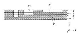
- FIG. 3 is a view of each divided pattern after the first processing as seen from the AA cross section of FIG. 2.
- FIG. 3 is a view of each divided pattern after the second processing as seen from the AA cross section of FIG. 2. It is a figure which shows the division
- FIG. 10 is a view of each divided pattern after the third processing as seen from the AA cross section of FIG. 2.
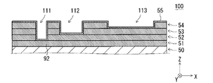
- FIG. 3 is a view of a manufacturing process of a multilayer three-dimensional structure as seen from the AA cross section of FIG.
- FIG. 3 is a view of a manufacturing process of a multilayer three-dimensional structure as seen from the AA cross section of FIG.
- FIG. 3 is a view of a manufacturing process of a multilayer three-dimensional structure as seen from the AA cross section of FIG.
- FIG. 3 is a view of a manufacturing process of a multilayer three-dimensional structure as seen from the AA cross section of FIG.
- FIG. 3 is a view of a manufacturing process of a multilayer three-dimensional structure as seen from the AA cross section of FIG.
- FIG. 3 is a view of a manufacturing process of a multilayer three-dimensional structure as seen from the AA cross section of FIG.
- FIG. 3 is a view of a manufacturing process of a multilayer three-dimensional structure
- FIG. 3 is a view of a manufacturing process of a multilayer three-dimensional structure as seen from the AA section of FIG.
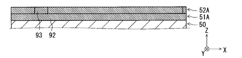
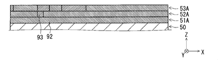
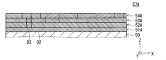
- FIG. 3 is a view of a manufacturing process of a multilayered three-dimensional structure according to a comparative example as seen from the AA cross section of FIG. 2 when a deviation occurs in the exposure position.
- FIG. 3 is a view of a manufacturing process of a multilayered three-dimensional structure according to a comparative example as seen from the AA cross section of FIG. 2 when a deviation occurs in the exposure position.
- FIG. 3 is a view of a manufacturing process of a multilayered three-dimensional structure according to a comparative example as seen from the AA cross section of FIG. 2 when a deviation occurs in the exposure position.
- FIG. 3 is a view of a manufacturing process of a multilayered three-dimensional structure according to a comparative example as seen from the AA cross section of FIG. 2 when a deviation occurs in the exposure position.
- FIG. 3 is a view of a manufacturing process of a multilayered three-dimensional structure according to a comparative example as seen from the AA cross section of FIG. 2 when a deviation occurs in the exposure position.
- FIG. 3 is a view of a manufacturing process of a multilayered three-dimensional structure according to a comparative example as seen from the AA cross section of FIG. 2 when a deviation occurs in the exposure position.
- FIG. 3 is a view of a manufacturing process of a multilayered three-dimensional structure according to the present embodiment as seen from the AA cross section of FIG. 2 when a deviation occurs in the exposure position.
- FIG. 3 is a view of a manufacturing process of a multilayered three-dimensional structure according to the present embodiment as seen from the AA cross section of FIG. 2 when a deviation occurs in the exposure position.
- FIG. 3 is a view of a manufacturing process of a multilayered three-dimensional structure according to the present embodiment as seen from the AA cross section of FIG. 2 when a deviation occurs in the exposure position.
- FIG. 3 is a view of a manufacturing process of a multilayered three-dimensional structure according to the present embodiment as seen from the AA cross section of FIG. 2 when a deviation occurs in the exposure position.
- FIG. 3 is a view of a manufacturing process of a multilayered three-dimensional structure according to the present embodiment as seen from the AA cross section of FIG. 2 when a deviation occurs in the exposure position.
- FIG. 3 is a view of a manufacturing process of a multilayered three-dimensional structure according to the present embodiment as seen from the AA cross section of FIG. 2 when a deviation occurs in the exposure position.
- FIG. 1 is a flowchart showing the flow of exposure data generation processing for generating a plurality of exposure data and manufacturing processing for manufacturing the multilayer three-dimensional structure 100. Steps S1 and S2 in FIG. 1 show the steps of the exposure data generation process, and steps S3 to S10 in FIG. 1 show the steps of the manufacturing process.
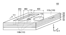
- FIG. 2 is a perspective view showing an example of the multilayer three-dimensional structure 100 manufactured by the flow of FIG.
- the multilayer structure 100 of the present embodiment is a structure in which four resist layers 51 to 54 are laminated on the main surface on the + Z side of the substrate 50, and the uneven surface 110 is formed on the + Z side.
- the concavo-convex surface 110 includes a rectangular first recess 111 having a long side in the Y direction in the XY plan view, an L-shaped second recess 112 having a long side in the Y direction in the XY plan view, and an XY plan view.
- the circular third recesses 113 are arranged along the X direction.
- the layers are called in order, they are called the first layer to the fourth layer in order from the ⁇ Z side layer to the + Z side layer.
- the uppermost surface (upper surface of the fourth layer) of the concavo-convex surface 110 is referred to as a convex surface 110a
- the portion of the concavo-convex surface 110 that is recessed from the convex surface 110a is referred to as a concave surface 110b.
- the first recess 111 is a recess having a depth corresponding to three layers. That is, the concave surface 110b of the first concave portion 111 is located at the boundary between the first layer and the second layer.
- the second recess 112 is a recess having a depth corresponding to two layers. That is, the concave surface 110b of the second concave portion 112 is located at the boundary between the second layer and the third layer.
- the third recess 113 is a recess having a depth corresponding to one layer. That is, the concave surface 110b of the third recess 113 is located at the boundary between the third layer and the fourth layer.
- FIG. 3 is a block diagram showing an electrical configuration of the exposure data generation apparatus 7 that executes the exposure data generation process.
- the exposure data generation device 7 is configured by a general computer in which, for example, a CPU 71, a ROM 72, a RAM 73, a storage device 74, and the like are interconnected via a bus line 75.
- the ROM 72 stores an operating system and the like, and the RAM 73 is used as a work area when the CPU 71 performs predetermined processing.
- the storage device 74 is configured by a nonvolatile storage device such as a flash memory or a hard disk device.
- the input unit 76, the display unit 77, the communication unit 78, and the reading unit 79 are also connected to the bus line 75.
- the input unit 76 includes various switches, a touch panel, and the like, and receives various inputs from the operator.
- the display unit 77 includes a liquid crystal display device, a lamp, and the like, and displays various types of information under the control of the CPU 71.
- the communication unit 78 has a data communication function via wire or wireless.
- the reading unit 79 reads data recorded on a recording medium readable by an inserted computer, for example, a CD, a DVD, or a USB memory.
- the program P (exposure data generation program) is installed in the exposure data generation device 7 and is executed in the RAM 73 (memory) by the CPU 71, so that the division pattern generation means that is a functional part of the exposure data generation device 7 executes step S1. Then, the data generation means that is a functional part of the exposure data generation device 7 executes step S2. Thereby, exposure data generation processing is executed.
- the program P may be read into the exposure data generation device 7 wirelessly. Further, the recording medium RM that records the program P so as to be readable by the computer may be read by the reading unit 79 and the program P may be read by the exposure data generating device 7.
- Step S1 division pattern generation step.
- the multilayer three-dimensional structure 100 is a three-dimensional structure composed of four layers, four division patterns are generated in step S1.
- step S2 data generation step
- the first process is performed. Specifically, for the four division patterns obtained in the division pattern generation step, the existence area of the multilayer three-dimensional structure 100 is set as the exposure area 90, and the non-existence area of the multilayer three-dimensional structure 100 is designated as the non-exposure area 91.
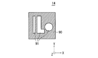
- Is set. 4 to 7 are diagrams showing the four divided patterns 11 to 14 after the first processing in the order of the first layer to the fourth layer.
- the first concave portion 111 to the third concave portion 113 are not formed in the first layer of the multilayer three-dimensional structure 100.
- the entire region of the first layer becomes the existence region of the multilayer three-dimensional structure 100.
- the entire first layer area is set as the exposure area 90.
- the first recess 111 is formed in the second layer of the multilayer structure 100, and the second recess 112 and the third recess 113 are not formed.
- the region where the first recess 111 is formed in the entire region of the second layer is a non-existing region of the multilayer three-dimensional structure 100, and the remaining region of the entire region of the second layer is the existing region of the multilayer three-dimensional structure 100. It becomes. Therefore, in the divided pattern 12, the non-existing area is set as the non-exposed area 91 among the entire area of the second layer, and the existing area is set as the exposed area 90 of the entire area of the second layer.
- the first recess 111 and the second recess 112 are formed in the third layer of the multilayer three-dimensional structure 100, and the third recess 113 is not formed.
- the region where the first concave portion 111 and the second concave portion 112 are formed in the entire region of the third layer is a non-existing region of the multilayer three-dimensional structure 100, and the remaining region of the entire third layer region is the multilayer solid This is the region where the structure 100 exists.
- the non-existing area is set as the non-exposed area 91 among the entire area of the third layer, and the existing area is set as the exposed area 90 among all the areas of the third layer.
- a first recess 111 to a third recess 113 are formed in the fourth layer of the multilayer structure 100.
- the region where the first recesses 111 to the third recess 113 are formed in the entire region of the fourth layer is a non-existing region of the multilayer three-dimensional structure 100, and the remaining region of the entire region of the fourth layer is the multilayer solid. This is the region where the structure 100 exists. Therefore, in the divided pattern 14, the non-existing area is set as the non-exposed area 91 among the entire areas of the fourth layer, and the existing area of the all areas of the fourth layer is set as the exposed area 90.
- FIG. 8 is a view of the divided patterns 11 to 14 as viewed from the AA cross section of FIG. 2 at the time after the first processing.
- the second process is performed. Specifically, the area where the exposure area 90 is set also in the upper layer (+ Z side layer) of each exposure area 90 after the first processing is changed to a non-exposure area 91.
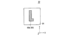
- 9 to 12 are diagrams showing the four divided patterns 21 to 24 after the second processing in the order of the first layer to the fourth layer.
- a region including the convex surface 110a on the + Z side is referred to as a convex surface region 90a
- a region including the concave surface 110b on the + Z side is referred to as a concave surface region 90b.
- the exposure region 90 in the divided pattern 21 is a concave region 90 b including the concave surface 110 b of the first concave portion 111 on the + Z side.
- the exposure region 90 in the divided pattern 22 is a concave region 90 b including the concave surface 110 b of the second concave portion 112 on the + Z side.
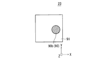
- the exposure region 90 in the divided pattern 23 is a concave region 90 b including the concave surface 110 b of the third concave portion 113 on the + Z side.
- the divided pattern 24 is the same pattern as the divided pattern 14.
- the exposure region 90 in the divided pattern 24 is a convex surface region 90a including a convex surface 110a on the + Z side.
- FIG. 13 is a view of the divided patterns 21 to 24 at the time after the second processing as seen from the AA cross section of FIG.
- the third process is performed next. Specifically, an area located around the concave surface area 90 b in each non-exposed area 91 after the second processing is changed to the exposure area 90.
- 14 to 17 are diagrams showing the four divided patterns 31 to 34 after the third process in the order of the first layer to the fourth layer.
- an area located around the concave surface 110b in each divided pattern is referred to as a concave peripheral area 90c.
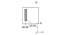
- the concave peripheral area 90c located around the concave area 90b in the non-exposure area 91 of the split pattern 21 is changed to the exposure area 90, and the split pattern 21 is changed to the split pattern 31. Is done.
- the concave surrounding area 90 c is a rectangular annular area having a long side in the Y direction.
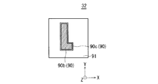
- the concave peripheral area 90c located around the concave area 90b in the non-exposure area 91 of the split pattern 22 is changed to the exposure area 90, and the split pattern 22 is changed to the split pattern 32. And changed.
- the concave peripheral region 90 c is an L-shaped annular region having a long side in the Y direction.
- the concave peripheral area 90c located around the concave area 90b in the non-exposed area 91 of the split pattern 23 is changed to the exposure area 90, and the split pattern 23 is changed to the split pattern 33. And changed.
- the concave surrounding area 90c is an annular area.
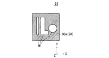
- the divided pattern 34 is the same pattern as the divided patterns 14 and 24.
- FIG. 18 is a view of the divided patterns 31 to 34 at the time after the third process, as viewed from the AA cross section of FIG.
- the data of the four divided patterns 31 to 34 generated in the first process to the third process become the four exposure data given to the exposure apparatus during the manufacturing process of the multilayer three-dimensional structure 100.
- the overlay accuracy of the exposure apparatus is known in advance before the third process, and the width W40 of the concave surrounding area 90c is set to twice the overlay accuracy.
- the overlay accuracy is an upper limit value of deviation when the exposure position when the resist layer is exposed deviates from the reference exposure position.
- the overlay accuracy in Japanese Unexamined Patent Application Publication No. 2009-224523 and Japanese Unexamined Patent Application Publication No. 2014 are provided. This is the same concept as the overlay accuracy in Japanese Patent Application No. 103343.
- the effect of setting the width W40 of the concave surrounding area 90c will be described in detail in ⁇ 1.4 Positional shift in exposure process> described later.
- a manufacturing system for manufacturing the multilayer three-dimensional structure 100 develops a resist laminate formed by repeatedly forming a resist layer and exposing the resist layer in each layer, and has a three-dimensional three-dimensional structure having an uneven surface 110 on the + Z side.
- 100 is a system for manufacturing 100.
- This manufacturing system includes an exposure data generating device 7, a coating device that coats a resist to form a resist layer, a heating device that heats the resist layer, an exposure device that exposes the resist layer, and an exposure device that is not exposed.
- a developing device that removes the resist at the spot with a developer, and a surface processing device that performs surface processing.
- the manufacturing system may be configured by arranging these devices in a cluster system, or may be configured by arranging these devices in an inline system.
- FIG. 19 to FIG. 24 are views showing the manufacturing process of the multilayer three-dimensional structure 100 as seen from the AA cross section of FIG.
- the manufacturing process of the multilayer three-dimensional structure 100 when viewed from the AA cross section of FIG. 2 will be described.
- the coating apparatus applies a negative resist to the main surface on one side (+ Z side) of the substrate 50 to form the first resist layer 51 on the substrate 50 (step S3).
- This resist has transparency to exposure light used in the exposure apparatus.
- the heating device heats the resist layer 51 to evaporate the solvent in the resist layer 51 (step S4: pre-baking step).
- the exposure apparatus exposes the resist layer 51 based on the exposure data of the first layer among the four exposure data generated by the above-described exposure data generation process (step S5: exposure process).
- a portion of the resist layer 51 corresponding to the exposure region 90 of the divided pattern 31 is exposed to become a development insoluble region 92. Further, the portion corresponding to the non-exposed area 91 of the divided pattern 31 in the resist layer 51 is not exposed and is maintained as the development soluble area 93.
- the exposure apparatus is composed of, for example, a direct drawing apparatus that continuously performs local exposure by irradiating the resist layer with exposure light while scanning. In this case, the direct drawing process is executed in step S5, and it is not necessary to prepare a mask corresponding to each exposure data.
- FIG. 19 is a diagram showing a manufacturing process of the multilayer three-dimensional structure 100 at this point.
- Step S7 When Steps S3 to S6 are executed for the resist layer 51, it is determined whether or not there is a resist layer that has not yet been formed (Step S7). Here, since the resist layers 52 to 54 exist as resist layers not yet formed, the process branches to Yes in step S7.
- Steps S3 to S6 are executed for the second resist layer 52 on the substrate 50.
- a portion corresponding to the exposure region 90 of the divided pattern 32 in the resist layer 52 is exposed to become a development insoluble region 92.
- the resist used in the present embodiment is transmissive to exposure light.
- the resist layer 51 which is the lower layer of the resist layer 52, is also exposed at a portion corresponding to the exposure region 90 of the divided pattern 32 to become a development insoluble region 92.
- the portion corresponding to the non-exposed area 91 of the divided pattern 32 in the resist layer 52 is not exposed and is maintained as the development soluble area 93.
- the resist layer 52 is heated, and the solvent in the resist layer 52 evaporates.
- FIG. 20 is a diagram illustrating a manufacturing process of the multilayered three-dimensional structure 100 at this point.
- Step S7 When Steps S3 to S6 are executed for the resist layer 52, it is determined whether or not there is a resist layer that has not yet been formed (Step S7). Here, since the resist layers 53 and 54 exist as resist layers not yet formed, the process branches to Yes in step S7.
- FIG. 21 is a diagram showing a manufacturing process of the multilayer structure 100 when Steps S3 to S6 are performed on the resist layer 53.
- FIG. 22 is a diagram showing a manufacturing process of the multilayer structure 100 when Steps S3 to S6 are performed on the resist layer.
- the resist laminate 57 is generated by executing steps S3 to S6 for each layer in the order from the ⁇ Z side to the + Z side. Then, it is determined whether or not there is a resist layer that has not yet been formed (step S7). Since all the resist layers 51 to 54 are formed here, the process branches to No in step S7.
- the developing device removes the resist in the development soluble region 93 of the resist laminated body 57 with the developer to obtain the multilayer three-dimensional structure 100 (step S8: development step). At this point, the multilayer three-dimensional structure 100 is obtained, but the strength of the multilayer three-dimensional structure 100 is increased by performing steps S9 and S10 in the manufacturing process.
- FIG. 23 is a diagram illustrating a manufacturing process of the multilayered three-dimensional structure 100 at this point.
- the multilayer three-dimensional structure 100 that is, the multilayer three-dimensional structure 100 corresponding to FIG. 23
- the next surface processing step is drawn. Yes.
- the surface processing apparatus processes the surface on the + Z side of the multilayer three-dimensional structure 100 and covers the surface with the protective film 55 (step S10: surface processing step).
- a film such as a plating film or a diamond-like carbon film is formed as the protective film 55.
- FIG. 24 is a diagram showing the multilayer three-dimensional structure 100 manufactured by steps S1 to S10.
- the multi-dimensional three-dimensional structure 100 is developed by developing the resist laminate 57 that is generated by repeatedly forming a resist layer and selectively exposing the resist layer in each layer. Manufacturing. For this reason, the depth of each recessed part in the uneven
- the multilayer three-dimensional structure 100 is used as, for example, an intaglio in printing processing.
- a relatively wide recess is formed relatively shallow among the plurality of recesses, and a relatively narrow recess among the plurality of recesses is relatively It is desirable to be formed deeply. This is because, when the ink filled in each recess is transferred to a transfer roll or the like, variation in the ink transfer ratio in each recess is suppressed.
- the width of the concave portion means a width in a short direction in a plan view of the concave portion as viewed from above. As shown in FIG.
- the third recess 113 having a relatively wide width W30 is formed relatively shallow, and the second recess 112 having an intermediate width W20 is set to an intermediate depth.
- the first concave portion 111 having a relatively narrow width W10 is formed relatively deep. For this reason, from the above viewpoint, variation during transfer is suppressed, which is desirable.
- the adhesion between the base material 50 and the resist layers 51 to 54 is increased, desirable.
- the components of the resist applied by the coating apparatus are the same in each layer as in this embodiment, compared to the embodiment in which the components of the resist are different in each layer as in the technique described in JP 2012-208350 A.
- the manufacturing process of the multilayer structure 100 is facilitated, and the manufacturing cost is also suppressed.
- the resist is applied to each resist layer as in the technique described in JP 2012-208350 A. Compared to an aspect in which exposure light having different wavelengths corresponding to the components is irradiated, the manufacturing process of the multilayer structure 100 is facilitated, and the manufacturing cost is also suppressed.
- the difference in the manufacturing process between the present embodiment and the comparative example will be described assuming that a positional deviation occurs in the exposure process.
- the first resist layer 51 is exposed at the reference exposure position
- the second resist layer 52 is exposed with a deviation of the overlay accuracy in the ⁇ X direction from the reference exposure position
- the third resist layer 53 is exposed. Is assumed to be shifted from the reference exposure position in the + X direction by the overlay accuracy
- the fourth resist layer 54 is exposed from the reference exposure position by the overlay accuracy in the ⁇ X direction.
- the exposure process is executed using the data of the divided patterns 11 to 14 shown in FIG. 8 as exposure data.
- 25 to 29 are views of the manufacturing process of the multilayer three-dimensional structure 100A as seen from the AA cross section of FIG.
- steps S3 to S6 are executed for the first resist layer 51A on the substrate 50.
- a portion corresponding to the exposure region 90 of the divided pattern 11 in the resist layer 51A is exposed to become a development insoluble region 92.
- the resist layer 51A is heated, and the solvent in the resist layer 51A evaporates.
- FIG. 25 is a diagram showing a manufacturing process of the multilayer three-dimensional structure 100A at this point.
- Step S7 When Steps S3 to S6 are executed for the resist layer 51A, it is determined whether or not there is a resist layer that has not yet been formed (Step S7).
- the process branches to Yes in step S7.
- Steps S3 to S6 are similarly performed for the second to fourth resist layers 52A to 54A on the base material 50.
- the exposure process is executed with a deviation of the overlay accuracy in the ⁇ X direction from the reference exposure position.
- FIG. 26 is a diagram showing a manufacturing process of the multilayer structure 100 when Steps S3 to S6 are performed on the resist layer 52A.
- FIG. 27 is a diagram showing a manufacturing process of the multilayer structure 100 when Steps S3 to S6 are performed on the resist layer 53A.
- FIG. 28 is a diagram showing a manufacturing process of the multilayer structure 100 when Steps S3 to S6 are performed on the resist layer 54A.
- steps S3 to S6 are executed for each layer in the order from the ⁇ Z side to the + Z side, whereby the resist laminate 57A is generated (FIG. 28). Then, it is determined whether or not there is a resist layer that has not yet been formed (step S7). Here, since all the resist layers 51A to 54A are formed, the process branches to No in step S7.
- the developing device removes the resist in the development soluble region 93 of the resist laminate 57A with a developer to obtain the multilayer three-dimensional structure 100A (step S8: development step).
- the heating device heats the multilayer three-dimensional structure 100A to evaporate the solvent in the multilayer three-dimensional structure 100A and the developer attached to the multilayer three-dimensional structure 100A (step S9: hard baking process).
- FIG. 29 is a diagram showing a manufacturing process of the multilayer three-dimensional structure 100A at this point.
- the multilayer three-dimensional structure 100A thus manufactured includes the first concave portion 111A to the third concave portion 113A on the concave and convex surface 110A.
- the uneven surface 110A is different from the shape of the uneven surface 110 in the multilayer three-dimensional structure 100 when an ideal exposure process without positional deviation is executed. This is because the shape of the development soluble region 93 in the resist laminate 57 ⁇ / b> A becomes incompatible with the shape of the concavo-convex surface 110 due to the displacement of the exposure position.
- the manufacturing method of the comparative example cannot manufacture a multilayer three-dimensional structure having a desired uneven surface 110 when a deviation occurs in the exposure position.
- the exposure process is executed using the data of the divided patterns 31 to 34 shown in FIG. 18 as exposure data.
- 30 to 35 are views showing the manufacturing process of the multilayer three-dimensional structure 100B as seen from the AA cross section of FIG.
- steps S3 to S6 are executed for the first resist layer 51B on the substrate 50.
- a portion corresponding to the exposure region 90 of the divided pattern 31 in the resist layer 51B is exposed to become a development insoluble region 92.
- the portion corresponding to the non-exposed area 91 of the divided pattern 31 in the resist layer 51B is not exposed and is maintained as the development soluble area 93.
- the resist layer 51B is heated, and the solvent in the resist layer 51B evaporates.
- FIG. 30 is a diagram showing a manufacturing process of the multilayer three-dimensional structure 100B at this point.
- Step S7 When Steps S3 to S6 are executed for the resist layer 51B, it is determined whether or not there is a resist layer that has not yet been formed (Step S7). Here, since the resist layers 52B to 54B exist as resist layers not yet formed, the process branches to Yes in step S7.
- Steps S3 to S6 are similarly performed for the second to fourth resist layers 52B to 54B on the base material 50.
- the exposure process is executed with a deviation of the overlay accuracy in the ⁇ X direction from the reference exposure position.
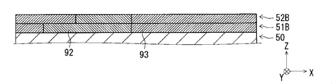
- FIG. 31 is a diagram showing a manufacturing process of the multilayer three-dimensional structure 100B at the time when Steps S3 to S6 are performed on the resist layer 52B.
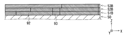
- FIG. 32 is a diagram showing a manufacturing process of the multilayer three-dimensional structure 100B at the time when Steps S3 to S6 are performed on the resist layer 53B.
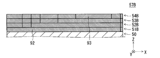
- FIG. 33 is a diagram showing a manufacturing process of the multilayer three-dimensional structure 100B when Steps S3 to S6 are performed on the resist layer 54B.
- steps S3 to S6 are executed for each layer in the order from the ⁇ Z side to the + Z side, whereby the resist laminate 57B is generated (FIG. 33). Then, it is determined whether or not there is a resist layer that has not yet been formed (step S7). Here, since all the resist layers 51B to 54B are formed, the process branches to No in step S7.
- the developing device removes the resist in the development soluble region 93 of the resist laminate 57B with a developer to obtain the multilayer three-dimensional structure 100B (step S8: development step).
- the heating device heats the multilayer three-dimensional structure 100B to evaporate the solvent in the multilayer three-dimensional structure 100B and the developer attached to the multilayer three-dimensional structure 100B (step S9: hard baking process).
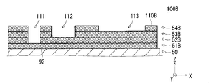
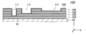
- FIG. 34 is a diagram showing a manufacturing process of the multilayer three-dimensional structure 100B at this point.
- the position of the concavo-convex surface 110B of the multilayer structure 100B manufactured in this way deviates from the ideal position (position of the concavo-convex surface 110) as the exposure position of the uppermost fourth layer is displaced. Formed. However, as can be seen from FIGS. 23 and 34, the shape of the uneven surface 110B of the multilayer three-dimensional structure 100B matches the ideal shape of the uneven surface 110.
- the exposure area 90 of the exposure data does not include other areas other than the convex surface area 90a, the concave surface area 90b, and the concave surface surrounding area 90c. Even in such a case, it is possible to suppress unintended steps.
- the exposure region 90 includes the other region, the fourth resist layer 54A is exposed to be shifted in the ⁇ X direction with respect to the third resist layer 53A. 2 An unintended step is formed in the recess 112A (FIGS. 27 to 29).
- the number of exposure areas is suppressed because the exposure area 90 includes only the convex area 90a, the concave area 90b, and the concave surrounding area 90c.
- the surface processing apparatus processes the surface on the + Z side of the multilayer three-dimensional structure 100B and covers the surface with the protective film 55B (step S10: surface processing step).
- a film such as a plating film or a diamond-like carbon film is formed as the protective film 55B.
- FIG. 35 is a diagram showing a multilayer three-dimensional structure 100B manufactured by steps S1 to S10.
- the aspect of manufacturing the multilayered three-dimensional structure 100 (FIG. 2) having a simple shape has been described.
- various types of multilayered three-dimensional structures can be manufactured according to the present invention.
- the layer thickness of each resist layer does not need to be constant.
- the width W40 of the concave surrounding area 90c is twice the overlay accuracy
- the present invention is not limited to this.
- the width of the concave peripheral region is at least twice the overlay accuracy.
- setting a wide exposure area causes an unintended step in the multilayer structure to be manufactured, and therefore the width of the concave peripheral area may be three times or less of the overlay accuracy. desirable.
- the multilayer structure 100 to be manufactured is formed of four resist layers.
- the manufactured multilayer three-dimensional structure 100 may be composed of three or less resist layers, or may be composed of five or more resist layers.
- the present invention is particularly effective when the number of layers is large, such as in the case of four or more layers, from the viewpoint of obtaining a multilayer three-dimensional structure having a desired concavo-convex surface even when the exposure position is shifted in each resist layer. It is.
- the mode in which a plurality of exposure data is generated by performing the first process to the third process has been described.
- the present invention is not limited to this. Even in a mode in which a plurality of exposure data is generated by another processing order, if the exposure area set in the exposure data includes a convex surface area, a concave surface area, and a concave peripheral area, the same effect as in the above embodiment is obtained. can get.
- the post-baking step (step S6) has an effect of promoting the crosslinking reaction of the heated resist layer and improving the adhesion between the resist layer and its upper and lower layers.
- the post-baking step (step S6) may be omitted.
- the exposure data generation method, the manufacturing method, the exposure data generation device, the exposure data generation program, and the manufacturing system have been described.
- the present invention can be freely combined with each embodiment, modified with any component in each embodiment, or omitted with any component in each embodiment.
- Exposure Data Generation Device 11-14 21-24, 31-34 Divided Pattern 50 Base Material 51-54, 51A-54A, 51B-54B Resist Layer 55, 55A, 55B Protective Film 57, 57A, 57B Resist Layer 90 Exposure region 90a Convex region 90b Concave surface region 90c Concave surface region 91 Non-exposed region 92 Development insoluble region 93 Development soluble region 100, 100A, 100B Multi-layer structure 110, 110A, 110B Concave surface 111, 111A First recess 112, 112A First 2 recesses 113, 113A 3rd recess S1-S10 steps
Landscapes
- Physics & Mathematics (AREA)
- General Physics & Mathematics (AREA)
- Engineering & Computer Science (AREA)
- Architecture (AREA)
- Structural Engineering (AREA)
- Exposure And Positioning Against Photoresist Photosensitive Materials (AREA)
- Photosensitive Polymer And Photoresist Processing (AREA)
- Materials For Photolithography (AREA)
Abstract
多層立体構造の製造に関して、凹凸面における各凹部の深さを個別に調整可能であり、かつ、露光位置の位置ズレに起因した凹凸面の形状変化を抑制可能な技術を提供する。本発明では、レジスト層の形成と当該レジスト層に対する選択的な露光とを各層で繰り返し行って生成されるレジスト積層体を現像することにより多層立体構造を製造する。このため、各レジスト層についての各露光パターンに応じて、凹凸面における各凹部の深さを個別に調整可能である。また、本発明では、露光データの露光領域が、凸面領域、凹面領域、および、凹面周囲領域からなる。このため、ある2つのレジスト層に関して両層がずれて露光された場合であっても、多層立体構造の凹凸面に意図しない段差が生じることが抑制される。
Description
本発明は、露光データに沿って露光することにより多層立体構造を製造する技術に関する。
従来より、積層されるレジストを選択的に露光した後、現像によってレジスト積層体のうち現像可溶領域を除去して、一方側に凹凸面を有する多層立体構造を製造する技術が知られている。
一方側に凹凸面を有する多層立体構造の製造方法としては、例えば、レジスト積層体の一方側の主面に耐エッチング液用のレジスト被膜を部分的に形成した後、被膜のない箇所についてウェットエッチングを行う技術が知られている。しかしながら、このようにウェットエッチングによって凹凸面を形成する場合、凹凸面における各凹部の深さを個別に調整することが困難である。
特許文献1に記載の技術では、レジストの成分が異なる複数のレジスト層を積層した後、波長の異なる複数の露光用光をレジスト積層体に照射してレジスト積層体を選択的に露光する。その後、現像によってレジスト積層体のうち現像可溶領域を除去して、多層立体構造を製造する。この技術では、凹凸面における各凹部の深さを個別に調整した多層立体構造を製造可能である。
しかしながら、特許文献1のようにレジストの成分が各層において異なる場合、それぞれ異なる成分のレジストを塗布する複数の塗布装置を設ける必要がある。また、特許文献1のように各レジスト層に対して波長の異なる複数の露光用光を照射する場合、それぞれ異なる波長の露光用光を照射する複数の露光装置を設ける必要がある。したがって、多層立体構造を製造する製造処理の容易性や製造コストの観点から望ましくない。
また、レジスト層に対する露光位置に全く位置ズレが生じないことは稀であり、通常は多少の位置ズレが生じる。この場合、特許文献1に記載の技術では、各レジスト層を露光する際の位置ズレに起因して、所望の形状とは異なる形状の凹凸面を有する多層立体構造が製造されることになる。したがって、各レジスト層を露光する際にこのような位置ズレが生じた場合であっても、所望の凹凸面を有する多層立体構造を製造可能な技術が求められている。
本発明は上記課題に鑑みなされたものであり、多層立体構造の製造に関して、凹凸面における各凹部の深さを個別に調整可能であり、かつ、露光位置の位置ズレに起因した凹凸面の形状変化を抑制可能な技術を提供することを目的としている。
本発明の第1の態様にかかる露光データ生成方法は、レジスト層の形成と当該レジスト層に対する露光とを各層で繰り返し行って生成されるレジスト積層体を現像して多層立体構造を製造することに先立って、複数の露光データを生成する露光データ生成方法であって、一方側に凹凸面を有する前記多層立体構造を表現した設計データを基に、前記多層立体構造を深さ方向で前記各層に分割した場合の各パターンを表現した複数の分割パターンを生成する分割パターン生成工程と、前記複数の分割パターンに対して、前記一方側に凸面を含む凸面領域、前記一方側に凹面を含む凹面領域、および、前記凹面領域の周囲に位置する凹面周囲領域を、露光領域として設定して、複数の露光データを生成するデータ生成工程と、を備えることを特徴とする。
本発明の第2の態様にかかる露光データ生成方法は、本発明の第1の態様にかかる露光データ生成方法であって、前記データ生成工程は、前記複数の分割パターンに対して、前記多層立体構造の存在領域を露光領域として設定し前記多層立体構造の非存在領域を非露光領域として設定する第1処理と、前記第1処理後の各露光領域のうち前記一方側の層にも露光領域が設定される領域を非露光領域に変更することにより、前記凸面領域および前記凹面領域を露光領域として設定する第2処理と、前記第2処理後の各非露光領域のうち前記凹面領域の周囲に位置する前記凹面周囲領域を露光領域に変更することにより、前記凸面領域、前記凹面領域、および、前記凹面周囲領域を露光領域として設定して、前記複数の露光データを生成する第3処理と、を実行する工程であることを特徴とする。
本発明の第3の態様にかかる露光データ生成方法は、本発明の第1の態様または第2の態様にかかる露光データ生成方法であって、露光装置がレジスト層に対して露光をする際の露光位置が基準露光位置からズレる場合におけるズレの上限値が、重ね合わせ精度として予め知得されており、前記凹面周囲領域の幅は前記重ね合わせ精度の2倍ないし3倍の長さであることを特徴とする。
本発明の第4の態様にかかる露光データ生成方法は、本発明の第1の態様ないし第3の態様のいずれかにかかる露光データ生成方法であって、前記凹凸面は複数の凹部を有しており、前記複数の凹部のうち相対的に幅の広い凹部は相対的に浅く前記複数の凹部のうち相対的に幅の狭い凹部は相対的に深いことを特徴とする。
本発明の第5の態様にかかる製造方法は、レジスト層の形成と当該レジスト層に対する露光とを各層で繰り返し行って生成されるレジスト積層体を現像して、一方側に凹凸面を有する多層立体構造を製造する製造方法であって、他方側から前記一方側の順で各層に対して繰り返し実行される工程として、レジストを塗布してレジスト層を形成する塗布工程と、前記レジスト層を加熱するプリベーク工程と、本発明の第1の態様ないし第4の態様のいずれかにかかる露光データ生成方法により生成される前記複数の露光データのうちその層に対応する露光データに基づいて、前記レジスト層を露光する露光工程と、を有し、前記各層に対して前記塗布工程、前記プリベーク工程、および、前記露光工程が実行されて生成されるレジスト積層体に対して実行される工程として、前記露光工程で露光されなかった箇所のレジストを現像液により除去して、前記多層立体構造を得る現像工程と、前記多層立体構造を加熱するハードベーク工程と、を有することを特徴とする。
本発明の第6の態様にかかる製造方法は、本発明の第5の態様にかかる製造方法であって、前記他方側から前記一方側の順で各層に対して繰り返し実行される工程として、前記塗布工程、前記プリベーク工程、および、前記露光工程、に加え、露光された前記レジスト層を加熱するポストベーク工程、を有し、前記各層に対して前記塗布工程、前記プリベーク工程、前記露光工程、および、前記ポストベーク工程が実行されて生成されるレジスト積層体に対して実行される工程として、前記現像工程および前記ハードベーク工程を有することを特徴とする。
本発明の第7の態様にかかる製造方法は、本発明の第5の態様または第6の態様にかかる製造方法であって、前記ハードベーク工程の後に行われる工程として、前記多層立体構造の前記一方側の表面を加工する表面加工工程を有することを特徴とする。
本発明の第8の態様にかかる製造方法は、本発明の第5の態様ないし第7の態様のいずれかにかかる製造方法であって、前記塗布工程において塗布されるレジストの成分は前記各層において同一であることを特徴とする。
本発明の第9の態様にかかる製造方法は、本発明の第5の態様ないし第8の態様のいずれかにかかる製造方法であって、前記露光工程は、前記レジスト層に対して露光用光を走査しつつ照射することによって局所的な露光を連続的に行う直接描画工程であることを特徴とする。
本発明の第10の態様にかかる露光データ生成装置は、レジスト層の形成と当該レジスト層に対する露光とを各層で繰り返し行って生成されるレジスト積層体を現像して多層立体構造を製造することに先立って、複数の露光データを生成する露光データ生成装置であって、一方側に凹凸面を有する前記多層立体構造を表現した設計データを基に、前記多層立体構造を深さ方向で前記各層に分割した場合の各パターンを表現した複数の分割パターンを生成する分割パターン生成手段と、前記複数の分割パターンに対して、前記一方側に凸面を含む凸面領域、前記一方側に凹面を含む凹面領域、および、前記凹面領域の周囲に位置する凹面周囲領域を、露光領域として設定して、複数の露光データを生成するデータ生成手段と、を備えることを特徴とする。
本発明の第11の態様にかかる露光データ生成装置は、本発明の第10の態様にかかる露光データ生成装置であって、前記データ生成手段は、前記複数の分割パターンに対して、前記多層立体構造の存在領域を露光領域として設定し前記多層立体構造の非存在領域を非露光領域として設定する第1処理と、前記第1処理後の各露光領域のうち前記一方側の層にも露光領域が設定される領域を非露光領域に変更することにより、前記凸面領域および前記凹面領域を露光領域として設定する第2処理と、第2処理後の各非露光領域のうち前記凹面領域の周囲に位置する前記凹面周囲領域を露光領域に変更することにより、前記凸面領域、前記凹面領域、および、前記凹面周囲領域を露光領域として設定して、前記複数の露光データを生成する第3処理と、を有することを特徴とする。
本発明の第12の態様にかかる露光データ生成装置は、本発明の第10の態様または第11の態様にかかる露光データ生成装置であって、露光装置がレジスト層に対して露光をする際の露光位置が基準露光位置からズレる場合におけるズレの上限値が、重ね合わせ精度として予め知得されており、前記凹面周囲領域の幅は前記重ね合わせ精度の2倍ないし3倍の長さであることを特徴とする。
本発明の第13の態様にかかる露光データ生成装置は、本発明の第10の態様ないし第12の態様のいずれかにかかる露光データ生成装置であって、前記凹凸面は複数の凹部を有しており、前記複数の凹部のうち相対的に幅の広い凹部は相対的に浅く前記複数の凹部のうち相対的に幅の狭い凹部は相対的に深いことを特徴とする。
本発明の第14の態様にかかる露光データ生成プログラムは、コンピュータにインストールされてCPUによってメモリにおいて実行されることにより、前記コンピュータを本発明の第10の態様ないし第13の態様のいずれかにかかる露光データ生成装置として機能させることを特徴とする。
本発明の第15の態様にかかる製造システムは、レジスト層の形成と当該レジスト層に対する露光とを各層で繰り返し行って生成されるレジスト積層体を現像して、一方側に凹凸面を有する多層立体構造を製造する製造システムであって、本発明の第10の態様ないし第13の態様のいずれかにかかる露光データ生成装置と、レジストを塗布してレジスト層を形成する塗布装置と、前記レジスト層を加熱する加熱装置と、前記レジスト層を露光する露光装置と、前記露光装置で露光されなかった箇所のレジストを現像液により除去する現像装置と、を備えることを特徴とする。
本発明の第16の態様にかかる製造システムは、本発明の第15の態様にかかる製造システムであって、前記多層立体構造の前記一方側の表面を加工する表面加工装置を有することを特徴とする。
本発明の第17の態様にかかる製造システムは、本発明の第15の態様または第16の態様にかかる製造システムであって、前記塗布装置が塗布するレジストの成分は前記各層において同一であることを特徴とする。
本発明の第18の態様にかかる製造システムは、本発明の第15の態様ないし第17の態様のいずれかにかかる製造システムであって、前記露光装置は、前記レジスト層に対して露光用光を走査しつつ照射することによって局所的な露光を連続的に行う直接描画装置であることを特徴とする。
本発明では、レジスト層の形成と当該レジスト層に対する選択的な露光とを各層で繰り返し行って生成されるレジスト積層体を現像することにより多層立体構造を製造する。このため、各レジスト層についての各露光パターンに応じて、凹凸面における各凹部の深さを個別に調整可能である。
また、本発明では、露光データの露光領域が、凸面領域、凹面領域、および、凹面周囲領域からなる。このため、ある2つのレジスト層に関して両層がずれて露光された場合であっても、多層立体構造の凹凸面に意図しない段差が生じることが抑制される。
以下、本発明の実施形態を図面に基づいて説明する。図面では同様な構成および機能を有する部分に同じ符号が付され、重複説明が省略される。また、各図面は模式的に示されたものである。なお、一部の図面には、方向関係を明確にする目的で、Z軸を鉛直方向の軸としXY平面を水平面とするXYZ直交座標軸が適宜付されている。以下の説明で、単に上下と表現する場合、上とは+Z側を意味し、下とは-Z側を意味する。
<1 実施形態>
<1.1 多層立体構造100の構成例>
図1は、複数の露光データを生成する露光データ生成処理および多層立体構造100を製造する製造処理の流れを示すフロー図である。図1中のステップS1、S2は露光データ生成処理の各工程を示し、図1中のステップS3~S10は製造処理の各工程を示す。
<1.1 多層立体構造100の構成例>
図1は、複数の露光データを生成する露光データ生成処理および多層立体構造100を製造する製造処理の流れを示すフロー図である。図1中のステップS1、S2は露光データ生成処理の各工程を示し、図1中のステップS3~S10は製造処理の各工程を示す。
図2は、図1のフローにより製造される多層立体構造100の一例を示す斜視図である。図2に示すように、本実施形態の多層立体構造100は、基材50の+Z側の主面に4層のレジスト層51~54を積層した構造であり、その+Z側に凹凸面110を有する。凹凸面110には、XY平面視においてY方向を長辺とする矩形状の第1凹部111と、XY平面視においてY方向を長辺とするL字状の第2凹部112と、XY平面視において円状の第3凹部113と、がX方向に沿って配列される。
以下では、各層を順序付けて呼ぶ場合に、-Z側の層から+Z側の層に向けて順に1層目~4層目と呼ぶ。また、以下では、凹凸面110のうちの最も上側の面(4層目の上面)を凸面110aと呼び、凹凸面110のうちの凸面110aより窪んだ部分を凹面110bと呼ぶ。また、第1凹部111は3層分の深さを有する凹部である。すなわち、第1凹部111の凹面110bは1層目と2層目との境界に位置する。また、第2凹部112は、2層分の深さを有する凹部である。すなわち、第2凹部112の凹面110bは2層目と3層目との境界に位置する。また、第3凹部113は、1層分の深さを有する凹部である。すなわち、第3凹部113の凹面110bは3層目と4層目との境界に位置する。
<1.2 露光データ生成処理>
以下では、多層立体構造100の製造処理に先立って行われる露光データ生成処理について説明する。
以下では、多層立体構造100の製造処理に先立って行われる露光データ生成処理について説明する。
図3は、露光データ生成処理を実行する露光データ生成装置7の電気的構成を示したブロック図である。図3に示されるように、露光データ生成装置7は、例えば、CPU71、ROM72、RAM73、記憶装置74等が、バスライン75を介して相互接続された一般的なコンピュータによって構成される。ROM72はオペレーティングシステム等を格納しており、RAM73はCPU71が所定の処理を行う際の作業領域として供される。記憶装置74は、フラッシュメモリ、あるいは、ハードディスク装置等の不揮発性の記憶装置によって構成される。
また、露光データ生成装置7では、入力部76、表示部77、通信部78、および、読取部79もバスライン75に接続されている。入力部76は、各種スイッチ、タッチパネル等により構成されており、オペレータからの各種入力を受ける。表示部77は、液晶表示装置、ランプ等により構成されており、CPU71による制御のもと各種の情報を表示する。通信部78は、有線または無線を介したデータ通信機能を有する。読取部79は、挿入されたコンピュータによって読み取り可能な記録媒体、例えばCD、DVD、あるいはUSBメモリ、に記録されたデータを読み取る。
プログラムP(露光データ生成プログラム)が露光データ生成装置7にインストールされてCPU71によりRAM73(メモリ)において実行されることによって、露光データ生成装置7の機能部である分割パターン生成手段がステップS1を実行し、露光データ生成装置7の機能部であるデータ生成手段がステップS2を実行する。これにより、露光データ生成処理が実行される。
プログラムPは、無線により露光データ生成装置7に読み込まれてもよい。また、コンピュータによって読み取り可能にプログラムPを記録する記録媒体RMが読取部79に読み取られて、プログラムPが露光データ生成装置7に読み込まれてもよい。
露光データ生成処理では、まず、多層立体構造100を表現した設計データを基に、多層立体構造100を深さ方向で各層に分割した場合の各パターンを表現した複数の分割パターンが生成される(ステップS1:分割パターン生成工程)。ここでは、多層立体構造100が4層からなる立体構造であるので、ステップS1で4つの分割パターンが生成される。
露光データ生成処理では、次に、4つの分割パターンに対して第1処理ないし第3処理が行われて、4つの露光データが生成される(ステップS2:データ生成工程)。
データ生成工程では、まず、第1処理が行われる。具体的には、分割パターン生成工程で得られた4つの分割パターンに対して、多層立体構造100の存在領域が露光領域90として設定され、多層立体構造100の非存在領域が非露光領域91として設定される。図4~図7は、第1処理後の4つの分割パターン11~14を1層目~4層目の順に示す図である。
図2に示すように、多層立体構造100の1層目には、第1凹部111~第3凹部113が形成されていない。言い換えると、1層目の全ての領域が、多層立体構造100の存在領域となる。このため、分割パターン11においては、1層目の全ての領域が露光領域90として設定される。
また、図2に示すように、多層立体構造100の2層目には、第1凹部111が形成され、第2凹部112および第3凹部113は形成されていない。言い換えると、2層目の全領域のうち第1凹部111が形成された領域は多層立体構造100の非存在領域となり、2層目の全領域のうち残りの領域は多層立体構造100の存在領域となる。このため、分割パターン12においては、2層目の全領域のうち上記非存在領域が非露光領域91として設定され、2層目の全領域のうち上記存在領域が露光領域90として設定される。
また、図2に示すように、多層立体構造100の3層目には、第1凹部111および第2凹部112が形成され、第3凹部113は形成されていない。言い換えると、3層目の全領域のうち第1凹部111および第2凹部112が形成された領域は多層立体構造100の非存在領域となり、3層目の全領域のうち残りの領域は多層立体構造100の存在領域となる。このため、分割パターン13においては、3層目の全領域のうち上記非存在領域が非露光領域91として設定され、3層目の全領域のうち上記存在領域が露光領域90として設定される。
また、図2に示すように、多層立体構造100の4層目には、第1凹部111~第3凹部113が形成されている。言い換えると、4層目の全領域のうち第1凹部111~第3凹部113が形成された領域は多層立体構造100の非存在領域となり、4層目の全領域のうち残りの領域は多層立体構造100の存在領域となる。このため、分割パターン14においては、4層目の全領域のうち上記非存在領域が非露光領域91として設定され、4層目の全領域のうちの上記存在領域が露光領域90として設定される。図8は、この第1処理後の時点における分割パターン11~14を図2のA-A断面から見た図である。
データ生成工程では、次に、第2処理が行われる。具体的には、第1処理後の各露光領域90のうちその上層(+Z側の層)にも露光領域90が設定される領域が、非露光領域91に変更される。図9~図12は、第2処理後の4つの分割パターン21~24を1層目~4層目の順に示す図である。以下では、各分割パターンにおいて+Z側に凸面110aを含む領域を凸面領域90aと呼び、+Z側に凹面110bを含む領域を凹面領域90bと呼ぶ。
1層目に対する第2処理により、分割パターン11の露光領域90のうち分割パターン12~14にも露光領域90が設定される領域は非露光領域91に変更されて、分割パターン11は分割パターン21へと変更される。図2および図9から分かるように、分割パターン21における露光領域90は、+Z側に第1凹部111の凹面110bを含む凹面領域90bである。
また、2層目に対する第2処理により、分割パターン12の露光領域90のうち分割パターン13、14にも露光領域90が設定される領域は非露光領域91に変更されて、分割パターン12は分割パターン22へと変更される。図2および図10から分かるように、分割パターン22における露光領域90は、+Z側に第2凹部112の凹面110bを含む凹面領域90bである。
また、3層目に対する第2処理により、分割パターン13の露光領域90のうち分割パターン14にも露光領域90が設定される領域は非露光領域91に変更されて、分割パターン13は分割パターン23へと変更される。図2および図11から分かるように、分割パターン23における露光領域90は、+Z側に第3凹部113の凹面110bを含む凹面領域90bである。
また、4層目は多層立体構造100において最も上の層であるので、4層目に対して第2処理が行われても露光領域90および非露光領域91に変更はない。したがって、分割パターン24は分割パターン14と同様のパターンとなる。図2および図12から分かるように、分割パターン24における露光領域90は、+Z側に凸面110aを含む凸面領域90aである。
以上説明したように、第2処理後の分割パターン21~24では、凸面領域90aおよび凹面領域90bが露光領域90として設定される。図13は、この第2処理後の時点における分割パターン21~24を図2のA-A断面から見た図である。
データ生成工程では、次に、第3処理が行われる。具体的には、第2処理後の各非露光領域91のうち凹面領域90bの周囲に位置する領域が露光領域90に変更される。図14~図17は、第3処理後の4つの分割パターン31~34を1層目~4層目の順に示す図である。以下では、各分割パターンにおいて凹面110bの周囲に位置する領域を凹面周囲領域90cと呼ぶ。
1層目に対する第3処理により、分割パターン21の非露光領域91のうち凹面領域90bの周囲に位置する凹面周囲領域90cが露光領域90に変更されて、分割パターン21は分割パターン31へと変更される。図14から分かるように、凹面周囲領域90cはY方向を長辺とする矩形環状の領域である。
また、2層目に対する第3処理により、分割パターン22の非露光領域91のうち凹面領域90bの周囲に位置する凹面周囲領域90cが露光領域90に変更されて、分割パターン22は分割パターン32へと変更される。図15から分かるように、凹面周囲領域90cはY方向を長辺とするL字環状の領域である。
また、3層目に対する第3処理により、分割パターン23の非露光領域91のうち凹面領域90bの周囲に位置する凹面周囲領域90cが露光領域90に変更されて、分割パターン23は分割パターン33へと変更される。図16から分かるように、凹面周囲領域90cは円環状の領域である。
また、4層目の分割パターン24は凹面領域90bを有さないので、4層目に対して第3処理が行われても露光領域90および非露光領域91に変更はない。したがって、分割パターン34は分割パターン14、24と同様のパターンとなる。
以上説明したように、第3処理後の分割パターン31~34では、凸面領域90a、凹面領域90b、および、凹面周囲領域90cが露光領域90として設定される。図18は、この第3処理後の時点における分割パターン31~34を図2のA-A断面から見た図である。
こうして第1処理~第3処理で生成された4つの分割パターン31~34のデータが、多層立体構造100の製造処理の際に露光装置に与えられる4つの露光データとなる。
本実施形態では、露光装置の重ね合わせ精度が第3処理よりも前に予め知得され、凹面周囲領域90cの幅W40が重ね合わせ精度の2倍の長さに設定される。ここで、重ね合わせ精度とは、レジスト層に対して露光をする際の露光位置が基準露光位置からずれる場合におけるズレの上限値であり、特開2009-224523号公報におけるオーバーレイ精度や特開2014-103343号公報における重ね合わせ精度と同様の概念である。このように、凹面周囲領域90cの幅W40が設定されることの効果については、後述する<1.4 露光工程における位置ズレ>で詳細に説明する。
<1.3 多層立体構造100の製造処理>
多層立体構造100を製造する製造システムは、レジスト層の形成と当該レジスト層に対する露光とを各層で繰り返し行って生成されるレジスト積層体を現像して、+Z側に凹凸面110を有する多層立体構造100を製造するシステムである。
多層立体構造100を製造する製造システムは、レジスト層の形成と当該レジスト層に対する露光とを各層で繰り返し行って生成されるレジスト積層体を現像して、+Z側に凹凸面110を有する多層立体構造100を製造するシステムである。
この製造システムは、露光データ生成装置7と、レジストを塗布してレジスト層を形成する塗布装置と、レジスト層を加熱する加熱装置と、レジスト層を露光する露光装置と、露光装置で露光されなかった箇所のレジストを現像液により除去する現像装置と、表面加工を行う表面加工装置と、を備える。製造システムは、これら各装置をクラスタ方式で配置することにより構成されてもよいし、これら各装置をインライン方式で配置することにより構成されてもよい。
図19~図24は、多層立体構造100の製造過程を図2のA-A断面から見た図である。以下、図2のA-A断面から見た場合における、多層立体構造100の製造処理について説明する。
製造処理においては、まず、塗布装置が基材50の一方側(+Z側)の主面にネガ型のレジストを塗布し、基材50上における1層目のレジスト層51を形成する(ステップS3:塗布工程)。なお、このレジストは、露光装置で用いられる露光用光に対して透過性を有する。
次に、加熱装置が、レジスト層51を加熱して、レジスト層51内の溶剤を蒸発させる(ステップS4:プリベーク工程)。
次に、露光装置が、上述した露光データ生成処理により生成される4つの露光データのうち1層目の露光データに基づいて、レジスト層51を露光する(ステップS5:露光工程)。レジスト層51のうち分割パターン31の露光領域90に相当する箇所は、露光されて、現像不溶領域92となる。また、レジスト層51のうち分割パターン31の非露光領域91に相当する箇所は、露光されず、現像可溶領域93のまま維持される。露光装置は、例えば、レジスト層に対して露光用光を走査しつつ照射することによって局所的な露光を連続的に行う直接描画装置で構成される。この場合、ステップS5では直接描画工程が実行され、各露光データに対応するマスクを準備することが不要となるので望ましい。
次に、加熱装置がレジスト層51を加熱して、レジスト層51の溶剤を蒸発させる(ステップS6:ポストベーク工程)。図19は、この時点における、多層立体構造100の製造過程を示す図である。
レジスト層51についてステップS3~S6が実行されると、未だ形成されていないレジスト層が存在するか否かについて判定される(ステップS7)。ここでは、未だ形成されていないレジスト層としてレジスト層52~54が存在するため、ステップS7でYesに分岐する。
次に、基材50上における2層目のレジスト層52について、ステップS3~S6が実行される。その結果、レジスト層52のうち分割パターン32の露光領域90に相当する箇所は、露光されて、現像不溶領域92となる。上記の通り、本実施形態で用いられるレジストは露光用光に対して透過性を有する。このため、レジスト層52の下層であるレジスト層51についても、分割パターン32の露光領域90に相当する箇所が、露光されて、現像不溶領域92となる。また、レジスト層52のうち分割パターン32の非露光領域91に相当する箇所は、露光されず、現像可溶領域93のまま維持される。その後、レジスト層52が加熱されて、レジスト層52内の溶剤が蒸発する。図20は、この時点における、多層立体構造100の製造過程を示す図である。
レジスト層52についてステップS3~S6が実行されると、未だ形成されていないレジスト層が存在するか否かについて判定される(ステップS7)。ここでは、未だ形成されていないレジスト層としてレジスト層53、54が存在するため、ステップS7でYesに分岐する。
基材50上における3層目のレジスト層53および4層目のレジスト層54についても、同様にステップS3~S6が実行される。図21は、レジスト層53についてステップS3~S6を実行した時点における、多層立体構造100の製造過程を示す図である。図22は、レジスト層54についてステップS3~S6を実行した時点における、多層立体構造100の製造過程を示す図である。
このように、-Z側から+Z側の順で各層に対してステップS3~S6が実行されることにより、レジスト積層体57が生成される。そして、未だ形成されていないレジスト層が存在するか否かについて判定される(ステップS7)。ここでは、全てのレジスト層51~54が形成されているため、ステップS7でNoに分岐する。
現像装置は、レジスト積層体57のうち現像可溶領域93のレジストを現像液により除去して、多層立体構造100を得る(ステップS8:現像工程)。この時点で多層立体構造100は得られるが、製造処理では続けてステップS9、S10を行うことにより多層立体構造100の強度を高める。
次に、加熱装置は、多層立体構造100を加熱して、多層立体構造100内の溶剤や多層立体構造100に付着する現像液を蒸発させる(ステップS9:ハードベーク工程)。図23は、この時点における、多層立体構造100の製造過程を示す図である。なお、図2では、図示が煩雑になるのを防ぐ目的で、次の表面加工工程が行われる前の時点の多層立体構造100(すなわち、図23に対応する多層立体構造100)が描かれている。
次に、表面加工装置が、多層立体構造100の+Z側の表面を加工し、該表面を保護膜55で覆う(ステップS10:表面加工工程)。保護膜55として、例えば、めっき膜、または、ダイヤモンドライクカーボン膜などの膜が成膜される。図24は、ステップS1~S10により製造された多層立体構造100を示す図である。
以上説明したように、本実施形態の製造方法では、レジスト層の形成と当該レジスト層に対する選択的な露光とを各層で繰り返し行って生成されるレジスト積層体57を現像することにより多層立体構造100を製造する。このため、各レジスト層についての各露光パターンに応じて、凹凸面110における各凹部の深さを個別に調整可能である。
多層立体構造100は、例えば、印刷処理における凹版として利用される。多層立体構造100が凹版として利用される場合には、複数の凹部のうち相対的に幅の広い凹部は相対的に浅く形成され、前記複数の凹部のうち相対的に幅の狭い凹部は相対的に深く形成されることが望ましい。これにより、各凹部に充填されたインクを転写ロール等に転写する際に、各凹部におけるインク転写割合のばらつきが抑制されるからである。ここで、凹部の幅とは、その凹部を上面から視た平面視において短方向の幅をいう。図2に示すように、本実施形態の多層立体構造100では、相対的に広い幅W30の第3凹部113が相対的に浅く形成され、中間の幅W20の第2凹部112が中間の深さで形成され、相対的に狭い幅W10の第1凹部111が相対的に深く形成される。このため、上記観点から転写時のばらつきが抑制され、望ましい。
また、本実施形態の多層立体構造100のように、1層目のレジスト層51の全面が現像不溶領域92であれば、基材50とレジスト層51~54との間の密着性が高まり、望ましい。
また、本実施形態のように塗布装置が塗布するレジストの成分が各層において同一である態様では、特開2012-208350号公報に記載の技術のようにレジストの成分が各層において異なる態様に比べて、多層立体構造100の製造処理が容易となり製造コストも抑制される。
また、本実施形態のように露光装置が同一波長の露光用光をレジスト層に対して照射する態様では、特開2012-208350号公報に記載の技術のように各レジスト層に対してレジストの成分に対応して異なる波長の露光用光を照射する態様に比べて、多層立体構造100の製造処理が容易となり製造コストも抑制される。
<1.4 露光工程における位置ズレ>
上述した<1.3 多層立体構造100の製造処理>では、レジスト層に対する位置ズレがない理想的な露光位置(基準露光位置)で露光工程が行われる場合について説明した。しかしながら、露光工程を実行する場合、一般には、XY面内において重ね合わせ精度の範囲内で露光位置がずれる。
上述した<1.3 多層立体構造100の製造処理>では、レジスト層に対する位置ズレがない理想的な露光位置(基準露光位置)で露光工程が行われる場合について説明した。しかしながら、露光工程を実行する場合、一般には、XY面内において重ね合わせ精度の範囲内で露光位置がずれる。
以下、露光工程における位置ズレが生じた場合を想定し、本実施形態と比較例との製造処理の差異を説明する。ここでは、1層目のレジスト層51を基準露光位置で露光し、2層目のレジスト層52を基準露光位置から-X方向に重ね合わせ精度分ずれて露光し、3層目のレジスト層53を基準露光位置から+X方向に重ね合わせ精度分ずれて露光し、4層目のレジスト層54を基準露光位置から-X方向に重ね合わせ精度分ずれて露光する場合を想定する。
上記想定のもと、比較例の製造処理で多層立体構造100Aを製造する場合について説明する。この比較例では、図8に示す分割パターン11~14のデータを露光データとして、露光工程を実行する。図25~図29は、多層立体構造100Aの製造過程を図2のA-A断面から見た図である。
まず、基材50上における1層目のレジスト層51Aについて、ステップS3~S6が実行される。その結果、レジスト層51Aのうち分割パターン11の露光領域90に相当する箇所が露光されて、現像不溶領域92となる。その後、レジスト層51Aが加熱されて、レジスト層51A内の溶剤が蒸発する。図25は、この時点における、多層立体構造100Aの製造過程を示す図である。
レジスト層51AについてステップS3~S6が実行されると、未だ形成されていないレジスト層が存在するか否かについて判定される(ステップS7)。ここでは、未だ形成されていないレジスト層としてレジスト層52A~54Aが存在するため、ステップS7でYesに分岐する。
基材50上における2層目~4層目のレジスト層52A~54Aについても、同様にステップS3~S6が実行される。なお、各ステップS5では、上記の通り、基準露光位置から±X方向に重ね合わせ精度分ずれて露光工程が実行される。図26は、レジスト層52AについてステップS3~S6を実行した時点における、多層立体構造100の製造過程を示す図である。図27は、レジスト層53AについてステップS3~S6を実行した時点における、多層立体構造100の製造過程を示す図である。図28は、レジスト層54AについてステップS3~S6を実行した時点における、多層立体構造100の製造過程を示す図である。
このように、-Z側から+Z側の順で各層に対してステップS3~S6が実行されることにより、レジスト積層体57Aが生成される(図28)。そして、未だ形成されていないレジスト層が存在するか否かについて判定される(ステップS7)。ここでは、全てのレジスト層51A~54Aが形成されているため、ステップS7でNoに分岐する。
現像装置は、レジスト積層体57Aのうち現像可溶領域93のレジストを現像液により除去して、多層立体構造100Aを得る(ステップS8:現像工程)。次に、加熱装置は、多層立体構造100Aを加熱して、多層立体構造100A内の溶剤や多層立体構造100Aに付着する現像液を蒸発させる(ステップS9:ハードベーク工程)。図29は、この時点における、多層立体構造100Aの製造過程を示す図である。
こうして製造された多層立体構造100Aは、凹凸面110Aに第1凹部111A~第3凹部113Aを含んで構成される。しかしながら、凹凸面110Aは、位置ズレのない理想的な露光工程を実行した場合の多層立体構造100における凹凸面110の形状とは異なる。これは、露光位置の位置ズレによってレジスト積層体57Aにおける現像可溶領域93の形状が凹凸面110の形状と非対応になったことに起因する。このように、比較例の製造方法では、露光位置にずれが生じた場合に所望の凹凸面110をもつ多層立体構造を製造することができない。
次に、上記想定のもと、本実施形態の製造処理で多層立体構造100Bを製造する場合について説明する。以下では、図18に示す分割パターン31~34のデータを露光データとして、露光工程を実行する。図30~図35は、多層立体構造100Bの製造過程を図2のA-A断面から見た図である。
まず、基材50上における1層目のレジスト層51Bについて、ステップS3~S6が実行される。その結果、レジスト層51Bのうち分割パターン31の露光領域90に相当する箇所が露光されて、現像不溶領域92となる。また、レジスト層51Bのうち分割パターン31の非露光領域91に相当する箇所は、露光されず、現像可溶領域93のまま維持される。その後、レジスト層51Bが加熱されて、レジスト層51B内の溶剤が蒸発する。図30は、この時点における、多層立体構造100Bの製造過程を示す図である。
レジスト層51BについてステップS3~S6が実行されると、未だ形成されていないレジスト層が存在するか否かについて判定される(ステップS7)。ここでは、未だ形成されていないレジスト層としてレジスト層52B~54Bが存在するため、ステップS7でYesに分岐する。
基材50上における2層目~4層目のレジスト層52B~54Bについても、同様にステップS3~S6が実行される。なお、各ステップS5では、上記の通り、基準露光位置から±X方向に重ね合わせ精度分ずれて露光工程が実行される。図31は、レジスト層52BについてステップS3~S6を実行した時点における、多層立体構造100Bの製造過程を示す図である。図32は、レジスト層53BについてステップS3~S6を実行した時点における、多層立体構造100Bの製造過程を示す図である。図33は、レジスト層54BについてステップS3~S6を実行した時点における、多層立体構造100Bの製造過程を示す図である。
このように、-Z側から+Z側の順で各層に対してステップS3~S6が実行されることにより、レジスト積層体57Bが生成される(図33)。そして、未だ形成されていないレジスト層が存在するか否かについて判定される(ステップS7)。ここでは、全てのレジスト層51B~54Bが形成されているため、ステップS7でNoに分岐する。
現像装置は、レジスト積層体57Bのうち現像可溶領域93のレジストを現像液により除去して、多層立体構造100Bを得る(ステップS8:現像工程)。次に、加熱装置は、多層立体構造100Bを加熱して、多層立体構造100B内の溶剤や多層立体構造100Bに付着する現像液を蒸発させる(ステップS9:ハードベーク工程)。図34は、この時点における、多層立体構造100Bの製造過程を示す図である。
こうして製造された多層立体構造100Bの凹凸面110Bの位置は、最も上層である4層目の露光位置が位置ズレしていることに伴って、理想的な位置(凹凸面110の位置)からずれて形成される。とはいえ、図23および図34から分かるように、多層立体構造100Bの凹凸面110Bの形状は、理想的な凹凸面110の形状と一致する。
本実施形態では、露光データの露光領域90が、凸面領域90a、凹面領域90b、および、凹面周囲領域90c以外の他の領域を含まないことによって、ある2つのレジスト層に関して両層がずれて露光された場合であっても、意図しない段差が生じることが抑制される。例えば、比較例では、露光領域90が上記他の領域を含むことによって、3層目のレジスト層53Aに対して4層目のレジスト層54Aが-X方向にずれて露光された場合に、第2凹部112Aに意図しない段差が生じている(図27~図29)。しかしながら、本実施形態では、露光領域90が凸面領域90a、凹面領域90b、および、凹面周囲領域90cのみからなることによって、露光領域の数が抑制される。これにより、下層で形成される現像不溶領域92と上層で形成される現像不溶領域92との間で意図しない段差が生じることが抑制される。特に、本実施形態のように凹面周囲領域90cの幅W40が重ね合わせ精度の2倍の長さであれば、ある2つのレジスト層に関して両層が反対向きに最大限ずれて露光された場合であっても(すなわち、両層が反対向きに重ね合わせ精度分ずれて露光された場合であっても)、各凹部の形状が変化することが防がれる。このため、本実施形態の製造方法では、露光位置の位置ズレに起因した凹凸面110の形状変化が抑制される。
最後に、表面加工装置が、多層立体構造100Bの+Z側の表面を加工し、該表面を保護膜55Bで覆う(ステップS10:表面加工工程)。保護膜55Bとして、例えば、めっき膜、または、ダイヤモンドライクカーボン膜などの膜が成膜される。図35は、ステップS1~S10により製造された多層立体構造100Bを示す図である。
<2 変形例>
以上、本発明の実施の形態について説明したが、この発明はその趣旨を逸脱しない限りにおいて上述したもの以外に種々の変更を行うことが可能である。
以上、本発明の実施の形態について説明したが、この発明はその趣旨を逸脱しない限りにおいて上述したもの以外に種々の変更を行うことが可能である。
上記実施形態では、理解を容易にする目的で、簡易な形状の多層立体構造100(図2)を製造する態様について説明したが、本発明によって種々の形状の多層立体構造が製造可能である。また、上記実施形態では、各レジスト層の層厚が一定である場合について説明したが、各レジスト層の層厚は一定でなくても構わない。
また、上記実施形態では、凹面周囲領域90cの幅W40が重ね合わせ精度の2倍である場合について説明したが、これに限られるものではない。ただし、上記の通り、上層と下層との両層が反対向きにずれて露光される場合を考慮すると、凹面周囲領域の幅は重ね合わせ精度の2倍以上であることが望ましい。また、上記の通り、露光領域を広く設定することは製造される多層立体構造に意図しない段差を生じさせる原因となることから、凹面周囲領域の幅は重ね合わせ精度の3倍以下であることが望ましい。
また、上記実施形態では、製造される多層立体構造100が4層のレジスト層で構成される場合について説明したが、これに限られるものではない。製造される多層立体構造100は、3層以下のレジスト層で構成されてもよいし、5層以上のレジスト層で構成されてもよい。ただし、各レジスト層で露光位置がずれた場合であっても所望の凹凸面を持つ多層立体構造を得るという観点からいえば、4層以上の場合など層数が多い場合に本発明は特に有効である。
また、上記実施形態では、第1処理ないし第3処理を行うことによって複数の露光データが生成される態様について説明したが、これに限られるものではない。他の処理順序によって複数の露光データを生成する態様であっても、その露光データにおいて設定される露光領域が凸面領域、凹面領域、および凹面周囲領域からなれば、上記実施形態と同様の効果を得られる。
また、上記実施形態では、各レジスト層について露光工程(ステップS5)の後にポストベーク工程(ステップS6)を行う態様について説明した。一般に、ポストベーク工程(ステップS6)では、加熱されるレジスト層の架橋反応を促進させ該レジスト層とその上層および下層との密着性を向上させる効果がある。しかしながら、レジスト層の材質や形成されるレジスト層の層厚などの条件によっては、ポストベーク工程(ステップS6)を実施せずとも各層間での密着性を十分に確保することができる場合がある。したがって、このような場合、ポストベーク工程(ステップS6)は省略されても構わない。
以上、実施形態およびその変形例に係る露光データ生成方法、製造方法、露光データ生成装置、露光データ生成プログラム、および、製造システムについて説明したが、これらは本発明に好ましい実施形態の例であって、本発明の実施の範囲を限定するものではない。本発明は、その発明の範囲内において、各実施形態の自由な組み合わせ、あるいは各実施形態の任意の構成要素の変形、もしくは各実施形態において任意の構成要素の省略が可能である。
7 露光データ生成装置
11~14,21~24,31~34 分割パターン
50 基材
51~54,51A~54A,51B~54B レジスト層
55,55A,55B 保護膜
57,57A,57B レジスト積層体
90 露光領域
90a 凸面領域
90b 凹面領域
90c 凹面周囲領域
91 非露光領域
92 現像不溶領域
93 現像可溶領域
100,100A,100B 多層立体構造
110,110A,110B 凹凸面
111,111A 第1凹部
112,112A 第2凹部
113,113A 第3凹部
S1~S10 ステップ
11~14,21~24,31~34 分割パターン
50 基材
51~54,51A~54A,51B~54B レジスト層
55,55A,55B 保護膜
57,57A,57B レジスト積層体
90 露光領域
90a 凸面領域
90b 凹面領域
90c 凹面周囲領域
91 非露光領域
92 現像不溶領域
93 現像可溶領域
100,100A,100B 多層立体構造
110,110A,110B 凹凸面
111,111A 第1凹部
112,112A 第2凹部
113,113A 第3凹部
S1~S10 ステップ
Claims (18)
- レジスト層の形成と当該レジスト層に対する露光とを各層で繰り返し行って生成されるレジスト積層体を現像して多層立体構造を製造することに先立って、複数の露光データを生成する露光データ生成方法であって、
一方側に凹凸面を有する前記多層立体構造を表現した設計データを基に、前記多層立体構造を深さ方向で前記各層に分割した場合の各パターンを表現した複数の分割パターンを生成する分割パターン生成工程と、
前記複数の分割パターンに対して、前記一方側に凸面を含む凸面領域、前記一方側に凹面を含む凹面領域、および、前記凹面領域の周囲に位置する凹面周囲領域を、露光領域として設定して、複数の露光データを生成するデータ生成工程と、
を備えることを特徴とする露光データ生成方法。 - 請求項1に記載の露光データ生成方法であって、
前記データ生成工程は、
前記複数の分割パターンに対して、前記多層立体構造の存在領域を露光領域として設定し前記多層立体構造の非存在領域を非露光領域として設定する第1処理と、
前記第1処理後の各露光領域のうち前記一方側の層にも露光領域が設定される領域を非露光領域に変更することにより、前記凸面領域および前記凹面領域を露光領域として設定する第2処理と、
前記第2処理後の各非露光領域のうち前記凹面領域の周囲に位置する前記凹面周囲領域を露光領域に変更することにより、前記凸面領域、前記凹面領域、および、前記凹面周囲領域を露光領域として設定して、前記複数の露光データを生成する第3処理と、
を実行する工程であることを特徴とする露光データ生成方法。 - 請求項1または請求項2に記載の露光データ生成方法であって、
露光装置がレジスト層に対して露光をする際の露光位置が基準露光位置からズレる場合におけるズレの上限値が、重ね合わせ精度として予め知得されており、
前記凹面周囲領域の幅は前記重ね合わせ精度の2倍ないし3倍の長さであることを特徴とする露光データ生成方法。 - 請求項1ないし請求項3のいずれかに記載の露光データ生成方法であって、
前記凹凸面は複数の凹部を有しており、前記複数の凹部のうち相対的に幅の広い凹部は相対的に浅く前記複数の凹部のうち相対的に幅の狭い凹部は相対的に深いことを特徴とする露光データ生成方法。 - レジスト層の形成と当該レジスト層に対する露光とを各層で繰り返し行って生成されるレジスト積層体を現像して、一方側に凹凸面を有する多層立体構造を製造する製造方法であって、
他方側から前記一方側の順で各層に対して繰り返し実行される工程として、
レジストを塗布してレジスト層を形成する塗布工程と、
前記レジスト層を加熱するプリベーク工程と、
請求項1ないし請求項4のいずれかに記載の露光データ生成方法により生成される前記複数の露光データのうちその層に対応する露光データに基づいて、前記レジスト層を露光する露光工程と、
を有し、
前記各層に対して前記塗布工程、前記プリベーク工程、および、前記露光工程が実行されて生成されるレジスト積層体に対して実行される工程として、
前記露光工程で露光されなかった箇所のレジストを現像液により除去して、前記多層立体構造を得る現像工程と、
前記多層立体構造を加熱するハードベーク工程と、
を有することを特徴とする製造方法。 - 請求項5に記載の製造方法であって、
前記他方側から前記一方側の順で各層に対して繰り返し実行される工程として、
前記塗布工程、前記プリベーク工程、および、前記露光工程、に加え、露光された前記レジスト層を加熱するポストベーク工程、を有し、
前記各層に対して前記塗布工程、前記プリベーク工程、前記露光工程、および、前記ポストベーク工程が実行されて生成されるレジスト積層体に対して実行される工程として、
前記現像工程および前記ハードベーク工程を有することを特徴とする製造方法。 - 請求項5または請求項6に記載の製造方法であって、
前記ハードベーク工程の後に行われる工程として、前記多層立体構造の前記一方側の表面を加工する表面加工工程を有することを特徴とする製造方法。 - 請求項5ないし請求項7のいずれかに記載の製造方法であって、
前記塗布工程において塗布されるレジストの成分は前記各層において同一であることを特徴とする製造方法。 - 請求項5ないし請求項8のいずれかに記載の製造方法であって、
前記露光工程は、前記レジスト層に対して露光用光を走査しつつ照射することによって局所的な露光を連続的に行う直接描画工程であることを特徴とする製造方法。 - レジスト層の形成と当該レジスト層に対する露光とを各層で繰り返し行って生成されるレジスト積層体を現像して多層立体構造を製造することに先立って、複数の露光データを生成する露光データ生成装置であって、
一方側に凹凸面を有する前記多層立体構造を表現した設計データを基に、前記多層立体構造を深さ方向で前記各層に分割した場合の各パターンを表現した複数の分割パターンを生成する分割パターン生成手段と、
前記複数の分割パターンに対して、前記一方側に凸面を含む凸面領域、前記一方側に凹面を含む凹面領域、および、前記凹面領域の周囲に位置する凹面周囲領域を、露光領域として設定して、複数の露光データを生成するデータ生成手段と、
を備えることを特徴とする露光データ生成装置。 - 請求項10に記載の露光データ生成装置であって、
前記データ生成手段は、
前記複数の分割パターンに対して、前記多層立体構造の存在領域を露光領域として設定し前記多層立体構造の非存在領域を非露光領域として設定する第1処理と、
前記第1処理後の各露光領域のうち前記一方側の層にも露光領域が設定される領域を非露光領域に変更することにより、前記凸面領域および前記凹面領域を露光領域として設定する第2処理と、
第2処理後の各非露光領域のうち前記凹面領域の周囲に位置する前記凹面周囲領域を露光領域に変更することにより、前記凸面領域、前記凹面領域、および、前記凹面周囲領域を露光領域として設定して、前記複数の露光データを生成する第3処理と、
を有することを特徴とする露光データ生成装置。 - 請求項10または請求項11に記載の露光データ生成装置であって、
露光装置がレジスト層に対して露光をする際の露光位置が基準露光位置からズレる場合におけるズレの上限値が、重ね合わせ精度として予め知得されており、
前記凹面周囲領域の幅は前記重ね合わせ精度の2倍ないし3倍の長さであることを特徴とする露光データ生成装置。 - 請求項10ないし請求項12のいずれかに記載の露光データ生成装置であって、
前記凹凸面は複数の凹部を有しており、前記複数の凹部のうち相対的に幅の広い凹部は相対的に浅く前記複数の凹部のうち相対的に幅の狭い凹部は相対的に深いことを特徴とする露光データ生成装置。 - コンピュータにインストールされてCPUによってメモリにおいて実行されることにより、前記コンピュータを請求項10ないし請求項13のいずれかに記載の露光データ生成装置として機能させることを特徴とする露光データ生成プログラム。
- レジスト層の形成と当該レジスト層に対する露光とを各層で繰り返し行って生成されるレジスト積層体を現像して、一方側に凹凸面を有する多層立体構造を製造する製造システムであって、
請求項10ないし請求項13のいずれかに記載の露光データ生成装置と、
レジストを塗布してレジスト層を形成する塗布装置と、
前記レジスト層を加熱する加熱装置と、
前記レジスト層を露光する露光装置と、
前記露光装置で露光されなかった箇所のレジストを現像液により除去する現像装置と、
を備えることを特徴とする製造システム。 - 請求項15に記載の製造システムであって、
前記多層立体構造の前記一方側の表面を加工する表面加工装置を有することを特徴とする製造システム。 - 請求項15または請求項16に記載の製造システムであって、
前記塗布装置が塗布するレジストの成分は前記各層において同一であることを特徴とする製造システム。 - 請求項15ないし請求項17のいずれかに記載の製造システムであって、
前記露光装置は、前記レジスト層に対して露光用光を走査しつつ照射することによって局所的な露光を連続的に行う直接描画装置であることを特徴とする製造システム。
Priority Applications (2)
| Application Number | Priority Date | Filing Date | Title |
|---|---|---|---|
| KR1020177024361A KR20170108149A (ko) | 2015-03-30 | 2015-11-25 | 노광 데이터 생성 방법, 제조 방법, 노광 데이터 생성 장치, 노광 데이터 생성 프로그램, 및, 제조 시스템 |
| CN201580078204.XA CN107430345B (zh) | 2015-03-30 | 2015-11-25 | 曝光数据生成方法、多层立体结构的制造方法、曝光数据生成装置、计算机可读存储介质及多层立体结构的制造系统 |
Applications Claiming Priority (2)
| Application Number | Priority Date | Filing Date | Title |
|---|---|---|---|
| JP2015-068636 | 2015-03-30 | ||
| JP2015068636A JP6427452B2 (ja) | 2015-03-30 | 2015-03-30 | 露光データ生成方法、製造方法、露光データ生成装置、露光データ生成プログラム、および、製造システム |
Publications (1)
| Publication Number | Publication Date |
|---|---|
| WO2016157611A1 true WO2016157611A1 (ja) | 2016-10-06 |
Family
ID=57006664
Family Applications (1)
| Application Number | Title | Priority Date | Filing Date |
|---|---|---|---|
| PCT/JP2015/083016 Ceased WO2016157611A1 (ja) | 2015-03-30 | 2015-11-25 | 露光データ生成方法、製造方法、露光データ生成装置、露光データ生成プログラム、および、製造システム |
Country Status (5)
| Country | Link |
|---|---|
| JP (1) | JP6427452B2 (ja) |
| KR (1) | KR20170108149A (ja) |
| CN (1) | CN107430345B (ja) |
| TW (1) | TWI596445B (ja) |
| WO (1) | WO2016157611A1 (ja) |
Families Citing this family (2)
| Publication number | Priority date | Publication date | Assignee | Title |
|---|---|---|---|---|
| JP6840007B2 (ja) * | 2017-03-24 | 2021-03-10 | 株式会社Screenホールディングス | 凹版の製造方法および凹版製造装置 |
| JP7395410B2 (ja) | 2020-04-06 | 2023-12-11 | 株式会社Screenホールディングス | 光学装置および3次元造形装置 |
Citations (6)
| Publication number | Priority date | Publication date | Assignee | Title |
|---|---|---|---|---|
| JP2000199968A (ja) * | 1999-01-06 | 2000-07-18 | Sony Corp | 多層レジスト構造およびこれを用いた3次元微細構造の作製方法 |
| JP2002148817A (ja) * | 2000-11-14 | 2002-05-22 | Mitsubishi Materials Corp | レジストのパターニング方法、高アスペクト比のコンタクトプローブ及びその製法 |
| JP2005049460A (ja) * | 2003-07-30 | 2005-02-24 | Ricoh Co Ltd | レジストパターン作成方法、レジストパターン作成装置、フォトマスクの設計方法及びフォトマスク |
| JP2007114758A (ja) * | 2005-09-21 | 2007-05-10 | Tohoku Univ | 露光方法 |
| JP2007173826A (ja) * | 2005-12-24 | 2007-07-05 | Internatl Business Mach Corp <Ibm> | デュアル・ダマシン構造を製作する方法 |
| JP2012208350A (ja) * | 2011-03-30 | 2012-10-25 | Lapis Semiconductor Co Ltd | レジストパターンの形成方法、立体構造の製造方法、及び半導体装置の製造方法 |
Family Cites Families (3)
| Publication number | Priority date | Publication date | Assignee | Title |
|---|---|---|---|---|
| JP2747573B2 (ja) * | 1991-07-25 | 1998-05-06 | 富士通株式会社 | 露光データ作成装置及び露光データ作成方法 |
| JP4156700B2 (ja) * | 1998-03-16 | 2008-09-24 | 富士通株式会社 | 露光データ作成方法、露光データ作成装置、及び、記録媒体 |
| SG118239A1 (en) * | 2003-04-24 | 2006-01-27 | Asml Netherlands Bv | Lithographic processing method and device manufactured thereby |
-
2015
- 2015-03-30 JP JP2015068636A patent/JP6427452B2/ja not_active Expired - Fee Related
- 2015-11-25 WO PCT/JP2015/083016 patent/WO2016157611A1/ja not_active Ceased
- 2015-11-25 KR KR1020177024361A patent/KR20170108149A/ko not_active Abandoned
- 2015-11-25 CN CN201580078204.XA patent/CN107430345B/zh not_active Expired - Fee Related
-
2016
- 2016-03-23 TW TW105109066A patent/TWI596445B/zh not_active IP Right Cessation
Patent Citations (6)
| Publication number | Priority date | Publication date | Assignee | Title |
|---|---|---|---|---|
| JP2000199968A (ja) * | 1999-01-06 | 2000-07-18 | Sony Corp | 多層レジスト構造およびこれを用いた3次元微細構造の作製方法 |
| JP2002148817A (ja) * | 2000-11-14 | 2002-05-22 | Mitsubishi Materials Corp | レジストのパターニング方法、高アスペクト比のコンタクトプローブ及びその製法 |
| JP2005049460A (ja) * | 2003-07-30 | 2005-02-24 | Ricoh Co Ltd | レジストパターン作成方法、レジストパターン作成装置、フォトマスクの設計方法及びフォトマスク |
| JP2007114758A (ja) * | 2005-09-21 | 2007-05-10 | Tohoku Univ | 露光方法 |
| JP2007173826A (ja) * | 2005-12-24 | 2007-07-05 | Internatl Business Mach Corp <Ibm> | デュアル・ダマシン構造を製作する方法 |
| JP2012208350A (ja) * | 2011-03-30 | 2012-10-25 | Lapis Semiconductor Co Ltd | レジストパターンの形成方法、立体構造の製造方法、及び半導体装置の製造方法 |
Also Published As
| Publication number | Publication date |
|---|---|
| KR20170108149A (ko) | 2017-09-26 |
| JP6427452B2 (ja) | 2018-11-21 |
| CN107430345B (zh) | 2019-04-12 |
| TW201640231A (zh) | 2016-11-16 |
| CN107430345A (zh) | 2017-12-01 |
| TWI596445B (zh) | 2017-08-21 |
| JP2016188926A (ja) | 2016-11-04 |
Similar Documents
| Publication | Publication Date | Title |
|---|---|---|
| US8871408B2 (en) | Mask pattern creation method, recording medium, and semiconductor device manufacturing method | |
| JP2009294308A (ja) | パターン検証方法、パターン検証装置、プログラム、及び半導体装置の製造方法 | |
| KR100632328B1 (ko) | 패턴 데이터의 작성 방법, 패턴 검증 방법, 포토 마스크의작성 방법, 및 반도체 장치의 제조 방법 | |
| JP6418786B2 (ja) | パターンの作成方法、プログラムおよび情報処理装置 | |
| JP2011066238A (ja) | パターン形成用テンプレートの作製方法 | |
| US6221539B1 (en) | Mask pattern correction method and a recording medium which records a mask pattern correction program | |
| JP6730851B2 (ja) | 決定方法、形成方法、プログラム、および物品の製造方法 | |
| US20170220729A1 (en) | Directed Self-Assembly-Aware Layout Decomposition For Multiple Patterning | |
| KR20110012295A (ko) | 반도체 소자의 레이아웃 생성 방법 | |
| JP2019035874A (ja) | 半導体装置の製造方法 | |
| WO2016157611A1 (ja) | 露光データ生成方法、製造方法、露光データ生成装置、露光データ生成プログラム、および、製造システム | |
| JP5173701B2 (ja) | プリント配線板の配線パターンの形成方法およびプリント配線板の製造方法 | |
| US9104833B2 (en) | Mask set for double exposure process and method of using the mask set | |
| JP2008090286A (ja) | マスク及びその形成方法 | |
| TWI589987B (zh) | 光罩圖案的分割方法 | |
| CN106610563B (zh) | 掩膜版及双重图形化法的方法 | |
| JP2013161987A (ja) | パターン形成方法 | |
| JP2009271174A (ja) | マスクパターン作成方法及びパターン形成方法 | |
| CN104765247A (zh) | 一种亚微米光栅的制作方法 | |
| TWI597561B (zh) | 圖案產生方法、遮罩的製造方法、曝光方法、半導體設備的製造方法、儲存媒體、以及資訊處理裝置 | |
| JP6956516B2 (ja) | リソグラフィ方法、決定方法、情報処理装置、プログラム及び物品の製造方法 | |
| JP2010038944A (ja) | フォトマスクの製造方法及びこのフォトマスクを用いた半導体デバイスの製造方法 | |
| JP2018017762A (ja) | 凹版および凹版の製造方法 | |
| CN104752319B (zh) | 导电孔阵列图形的形成方法 | |
| JP3646713B2 (ja) | マスクパターン分割方法およびレジストパターン形成方法 |
Legal Events
| Date | Code | Title | Description |
|---|---|---|---|
| 121 | Ep: the epo has been informed by wipo that ep was designated in this application |
Ref document number: 15887753 Country of ref document: EP Kind code of ref document: A1 |
|
| ENP | Entry into the national phase |
Ref document number: 20177024361 Country of ref document: KR Kind code of ref document: A |
|
| NENP | Non-entry into the national phase |
Ref country code: DE |
|
| 122 | Ep: pct application non-entry in european phase |
Ref document number: 15887753 Country of ref document: EP Kind code of ref document: A1 |