WO2016157371A1 - 半導体装置および半導体装置の製造方法 - Google Patents
半導体装置および半導体装置の製造方法 Download PDFInfo
- Publication number
- WO2016157371A1 WO2016157371A1 PCT/JP2015/059956 JP2015059956W WO2016157371A1 WO 2016157371 A1 WO2016157371 A1 WO 2016157371A1 JP 2015059956 W JP2015059956 W JP 2015059956W WO 2016157371 A1 WO2016157371 A1 WO 2016157371A1
- Authority
- WO
- WIPO (PCT)
- Prior art keywords
- insulating film
- gate insulating
- metal
- semiconductor device
- film
- Prior art date
- Legal status (The legal status is an assumption and is not a legal conclusion. Google has not performed a legal analysis and makes no representation as to the accuracy of the status listed.)
- Ceased
Links
Images












Classifications
-
- H—ELECTRICITY
- H10—SEMICONDUCTOR DEVICES; ELECTRIC SOLID-STATE DEVICES NOT OTHERWISE PROVIDED FOR
- H10D—INORGANIC ELECTRIC SEMICONDUCTOR DEVICES
- H10D64/00—Electrodes of devices having potential barriers
- H10D64/60—Electrodes characterised by their materials
- H10D64/66—Electrodes having a conductor capacitively coupled to a semiconductor by an insulator, e.g. MIS electrodes
- H10D64/68—Electrodes having a conductor capacitively coupled to a semiconductor by an insulator, e.g. MIS electrodes characterised by the insulator, e.g. by the gate insulator
- H10D64/681—Electrodes having a conductor capacitively coupled to a semiconductor by an insulator, e.g. MIS electrodes characterised by the insulator, e.g. by the gate insulator having a compositional variation, e.g. multilayered
- H10D64/685—Electrodes having a conductor capacitively coupled to a semiconductor by an insulator, e.g. MIS electrodes characterised by the insulator, e.g. by the gate insulator having a compositional variation, e.g. multilayered being perpendicular to the channel plane
-
- H—ELECTRICITY
- H10—SEMICONDUCTOR DEVICES; ELECTRIC SOLID-STATE DEVICES NOT OTHERWISE PROVIDED FOR
- H10D—INORGANIC ELECTRIC SEMICONDUCTOR DEVICES
- H10D30/00—Field-effect transistors [FET]
- H10D30/40—FETs having zero-dimensional [0D], one-dimensional [1D] or two-dimensional [2D] charge carrier gas channels
- H10D30/47—FETs having zero-dimensional [0D], one-dimensional [1D] or two-dimensional [2D] charge carrier gas channels having two-dimensional [2D] charge carrier gas channels, e.g. nanoribbon FETs or high electron mobility transistors [HEMT]
- H10D30/471—High electron mobility transistors [HEMT] or high hole mobility transistors [HHMT]
- H10D30/475—High electron mobility transistors [HEMT] or high hole mobility transistors [HHMT] having wider bandgap layer formed on top of lower bandgap active layer, e.g. undoped barrier HEMTs such as i-AlGaN/GaN HEMTs
-
- H—ELECTRICITY
- H10—SEMICONDUCTOR DEVICES; ELECTRIC SOLID-STATE DEVICES NOT OTHERWISE PROVIDED FOR
- H10D—INORGANIC ELECTRIC SEMICONDUCTOR DEVICES
- H10D62/00—Semiconductor bodies, or regions thereof, of devices having potential barriers
- H10D62/80—Semiconductor bodies, or regions thereof, of devices having potential barriers characterised by the materials
- H10D62/85—Semiconductor bodies, or regions thereof, of devices having potential barriers characterised by the materials being Group III-V materials, e.g. GaAs
- H10D62/8503—Nitride Group III-V materials, e.g. AlN or GaN
-
- H—ELECTRICITY
- H10—SEMICONDUCTOR DEVICES; ELECTRIC SOLID-STATE DEVICES NOT OTHERWISE PROVIDED FOR
- H10D—INORGANIC ELECTRIC SEMICONDUCTOR DEVICES
- H10D64/00—Electrodes of devices having potential barriers
- H10D64/01—Manufacture or treatment
- H10D64/011—Manufacture or treatment of electrodes ohmically coupled to a semiconductor
-
- H—ELECTRICITY
- H10—SEMICONDUCTOR DEVICES; ELECTRIC SOLID-STATE DEVICES NOT OTHERWISE PROVIDED FOR
- H10D—INORGANIC ELECTRIC SEMICONDUCTOR DEVICES
- H10D64/00—Electrodes of devices having potential barriers
- H10D64/01—Manufacture or treatment
- H10D64/013—Manufacture or treatment of electrodes having a conductor capacitively coupled to a semiconductor by an insulator
- H10D64/01358—Manufacture or treatment of electrodes having a conductor capacitively coupled to a semiconductor by an insulator the insulator being formed after the semiconductor body, the semiconductor being a Group III-V material
-
- H—ELECTRICITY
- H10—SEMICONDUCTOR DEVICES; ELECTRIC SOLID-STATE DEVICES NOT OTHERWISE PROVIDED FOR
- H10D—INORGANIC ELECTRIC SEMICONDUCTOR DEVICES
- H10D64/00—Electrodes of devices having potential barriers
- H10D64/118—Electrodes comprising insulating layers having particular dielectric or electrostatic properties, e.g. having static charges
-
- H—ELECTRICITY
- H10—SEMICONDUCTOR DEVICES; ELECTRIC SOLID-STATE DEVICES NOT OTHERWISE PROVIDED FOR
- H10D—INORGANIC ELECTRIC SEMICONDUCTOR DEVICES
- H10D64/00—Electrodes of devices having potential barriers
- H10D64/20—Electrodes characterised by their shapes, relative sizes or dispositions
- H10D64/27—Electrodes not carrying the current to be rectified, amplified, oscillated or switched, e.g. gates
- H10D64/311—Gate electrodes for field-effect devices
- H10D64/411—Gate electrodes for field-effect devices for FETs
- H10D64/511—Gate electrodes for field-effect devices for FETs for IGFETs
- H10D64/512—Disposition of the gate electrodes, e.g. buried gates
- H10D64/513—Disposition of the gate electrodes, e.g. buried gates within recesses in the substrate, e.g. trench gates, groove gates or buried gates
-
- H—ELECTRICITY
- H10—SEMICONDUCTOR DEVICES; ELECTRIC SOLID-STATE DEVICES NOT OTHERWISE PROVIDED FOR
- H10D—INORGANIC ELECTRIC SEMICONDUCTOR DEVICES
- H10D64/00—Electrodes of devices having potential barriers
- H10D64/60—Electrodes characterised by their materials
- H10D64/66—Electrodes having a conductor capacitively coupled to a semiconductor by an insulator, e.g. MIS electrodes
- H10D64/667—Electrodes having a conductor capacitively coupled to a semiconductor by an insulator, e.g. MIS electrodes the conductor comprising a layer of alloy material, compound material or organic material contacting the insulator, e.g. TiN workfunction layers
-
- H—ELECTRICITY
- H10—SEMICONDUCTOR DEVICES; ELECTRIC SOLID-STATE DEVICES NOT OTHERWISE PROVIDED FOR
- H10D—INORGANIC ELECTRIC SEMICONDUCTOR DEVICES
- H10D64/00—Electrodes of devices having potential barriers
- H10D64/60—Electrodes characterised by their materials
- H10D64/66—Electrodes having a conductor capacitively coupled to a semiconductor by an insulator, e.g. MIS electrodes
- H10D64/68—Electrodes having a conductor capacitively coupled to a semiconductor by an insulator, e.g. MIS electrodes characterised by the insulator, e.g. by the gate insulator
- H10D64/691—Electrodes having a conductor capacitively coupled to a semiconductor by an insulator, e.g. MIS electrodes characterised by the insulator, e.g. by the gate insulator comprising metallic compounds, e.g. metal oxides or metal silicates
-
- H—ELECTRICITY
- H10—SEMICONDUCTOR DEVICES; ELECTRIC SOLID-STATE DEVICES NOT OTHERWISE PROVIDED FOR
- H10D—INORGANIC ELECTRIC SEMICONDUCTOR DEVICES
- H10D30/00—Field-effect transistors [FET]
- H10D30/01—Manufacture or treatment
- H10D30/015—Manufacture or treatment of FETs having heterojunction interface channels or heterojunction gate electrodes, e.g. HEMT
-
- H—ELECTRICITY
- H10—SEMICONDUCTOR DEVICES; ELECTRIC SOLID-STATE DEVICES NOT OTHERWISE PROVIDED FOR
- H10D—INORGANIC ELECTRIC SEMICONDUCTOR DEVICES
- H10D30/00—Field-effect transistors [FET]
- H10D30/01—Manufacture or treatment
- H10D30/021—Manufacture or treatment of FETs having insulated gates [IGFET]
-
- H—ELECTRICITY
- H10—SEMICONDUCTOR DEVICES; ELECTRIC SOLID-STATE DEVICES NOT OTHERWISE PROVIDED FOR
- H10D—INORGANIC ELECTRIC SEMICONDUCTOR DEVICES
- H10D30/00—Field-effect transistors [FET]
- H10D30/40—FETs having zero-dimensional [0D], one-dimensional [1D] or two-dimensional [2D] charge carrier gas channels
- H10D30/47—FETs having zero-dimensional [0D], one-dimensional [1D] or two-dimensional [2D] charge carrier gas channels having two-dimensional [2D] charge carrier gas channels, e.g. nanoribbon FETs or high electron mobility transistors [HEMT]
- H10D30/471—High electron mobility transistors [HEMT] or high hole mobility transistors [HHMT]
- H10D30/475—High electron mobility transistors [HEMT] or high hole mobility transistors [HHMT] having wider bandgap layer formed on top of lower bandgap active layer, e.g. undoped barrier HEMTs such as i-AlGaN/GaN HEMTs
- H10D30/4755—High electron mobility transistors [HEMT] or high hole mobility transistors [HHMT] having wider bandgap layer formed on top of lower bandgap active layer, e.g. undoped barrier HEMTs such as i-AlGaN/GaN HEMTs having wide bandgap charge-carrier supplying layers, e.g. modulation doped HEMTs such as n-AlGaAs/GaAs HEMTs
-
- H—ELECTRICITY
- H10—SEMICONDUCTOR DEVICES; ELECTRIC SOLID-STATE DEVICES NOT OTHERWISE PROVIDED FOR
- H10D—INORGANIC ELECTRIC SEMICONDUCTOR DEVICES
- H10D64/00—Electrodes of devices having potential barriers
- H10D64/20—Electrodes characterised by their shapes, relative sizes or dispositions
- H10D64/27—Electrodes not carrying the current to be rectified, amplified, oscillated or switched, e.g. gates
- H10D64/311—Gate electrodes for field-effect devices
- H10D64/411—Gate electrodes for field-effect devices for FETs
- H10D64/511—Gate electrodes for field-effect devices for FETs for IGFETs
- H10D64/517—Gate electrodes for field-effect devices for FETs for IGFETs characterised by the conducting layers
- H10D64/519—Gate electrodes for field-effect devices for FETs for IGFETs characterised by the conducting layers characterised by their top-view geometrical layouts
Definitions
- the present invention relates to a semiconductor device and a method for manufacturing the semiconductor device, and can be suitably used for, for example, a semiconductor device using a nitride semiconductor and a method for manufacturing the semiconductor device.
- a semiconductor device using a nitride semiconductor such as gallium nitride (GaN) has a characteristic of operating at high speed and low loss.
- a power MISFET (Metal-Insulator-Semiconductor-Field-Effect-Transistor) using a gallium nitride-based nitride semiconductor is capable of normally-off operation, and its development is in progress.
- Patent Document 1 Japanese Patent Application Laid-Open No. 2014-183125 describes an electron transit layer formed of i-GaN, an electron supply layer formed of AlGaN, a source electrode, a drain electrode, and an insulating film.
- a normally-off type semiconductor device having a formed gate electrode is disclosed.
- the gate electrode is formed by lift-off using Ni / Au.
- the present inventor is engaged in research and development of a semiconductor device using a nitride semiconductor as described above, and is eagerly examining improvement in characteristics of a normally-off type semiconductor device. In the process, it has been found that there is room for further improvement in a semiconductor device using a nitride semiconductor and a method for manufacturing the semiconductor device.
- a semiconductor device shown in an embodiment disclosed in the present application includes a first gate insulating film, a second gate insulating film, a first gate electrode, and a second gate electrode.
- the first gate insulating film is an oxide film containing a first metal or an oxide film containing silicon
- the second gate insulating film is an oxide film containing a second metal
- the electronegativity of the second metal is Less than the electronegativity of the first metal or silicon.
- the first gate electrode is a nitride film containing a third metal
- the second gate electrode is made of a fourth metal.
- a method of manufacturing a semiconductor device includes a step of forming a first gate insulating film made of an oxide film containing a first metal or an oxide film containing silicon on a nitride semiconductor layer. Have Forming a second gate insulating film made of an oxide film of a second metal on the first gate insulating film; and forming a first gate electrode made of a nitride film containing a third metal on the second gate insulating film. Forming. Furthermore, the method includes a step of forming a second gate electrode made of a fourth metal on the first gate electrode.
- the first gate insulating film is an oxide film containing a first metal or an oxide film containing silicon
- the second gate insulating film is an oxide film containing a second metal
- the electronegativity of the second metal is Less than the electronegativity of the first metal or silicon.
- the characteristics of the semiconductor device can be improved.
- a semiconductor device having good characteristics can be manufactured.
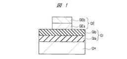
- FIG. 1 is a cross-sectional view illustrating a configuration of a semiconductor device according to a first embodiment.
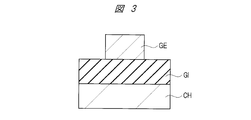
- FIG. 6 is a cross-sectional view showing another configuration of the semiconductor device of First Embodiment. 6 is a cross-sectional view showing a configuration of Comparative Example 1 of the semiconductor device of First Embodiment;
- FIG. 6 is a cross-sectional view showing a configuration of Comparative Example 2 of the semiconductor device of First Embodiment;
- FIG. FIG. 6 is a diagram showing oxygen concentration distributions in samples 1 to 4.
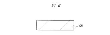
- 7 is a cross-sectional view showing a manufacturing step of the semiconductor device of First Embodiment;
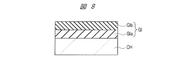
- FIG. 7 is a cross-sectional view showing a manufacturing step of the semiconductor device of the first embodiment, and is a cross-sectional view showing a manufacturing step following FIG. 6;
- FIG. 8 is a cross-sectional view showing a manufacturing step of the semiconductor device of the first embodiment, and is a cross-sectional view showing a manufacturing step following FIG. 7;
- FIG. 9 is a cross-sectional view showing a manufacturing step of the semiconductor device of the first embodiment, and is a cross-sectional view showing a manufacturing step following FIG. 8;
- FIG. 10 is a cross-sectional view showing a manufacturing step of the semiconductor device of the first embodiment, and is a cross-sectional view showing a manufacturing step following FIG. 9;
- FIG. 9 is a cross-sectional view showing a manufacturing step of the semiconductor device of the first embodiment, and is a cross-sectional view showing a manufacturing step following FIG. 9;
- FIG. 9 is a cross-sectional view showing a manufacturing step of the semiconductor device of the first embodiment
- FIG. 11 is a cross-sectional view showing a manufacturing step of the semiconductor device of the first embodiment, and is a cross-sectional view showing a manufacturing step following FIG. 10;
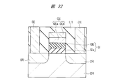
- 1 is a cross-sectional view showing a characteristic configuration of a semiconductor device according to a first embodiment.
- FIG. 6 is a cross-sectional view showing a configuration of a semiconductor device according to a second embodiment.
- 11 is a cross-sectional view showing a manufacturing step of the semiconductor device of Second Embodiment;
- FIG. FIG. 15 is a cross-sectional view showing a manufacturing step of the semiconductor device of the second embodiment, and showing the manufacturing step following FIG. 14;
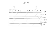
- FIG. 16 is a cross-sectional view showing a manufacturing step of the semiconductor device of the second embodiment, and is a cross-sectional view showing a manufacturing step following FIG. 15;
- FIG. 17 is a cross-sectional view showing a manufacturing step of the semiconductor device of the second embodiment, and is a cross-sectional view showing a manufacturing step following FIG. 16;
- FIG. 18 is a cross-sectional view showing a manufacturing step of the semiconductor device of the second embodiment, and showing the manufacturing step following FIG. 17;
- FIG. 19 is a cross-sectional view showing a manufacturing step of the semiconductor device of the second embodiment, and is a cross-sectional view showing a manufacturing step following FIG. 18;
- FIG. 18 is a cross-sectional view showing a manufacturing step of the semiconductor device of the second embodiment, and is a cross-sectional view showing a manufacturing step following FIG. 18;
- FIG. 20 is a cross-sectional view showing a manufacturing step of the semiconductor device of the second embodiment, and is a cross-sectional view showing a manufacturing step following FIG. 19;
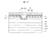
- FIG. 21 is a cross-sectional view showing a manufacturing step of the semiconductor device of the second embodiment, and is a cross-sectional view showing a manufacturing step following FIG. 20;
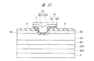
- FIG. 22 is a cross-sectional view showing a manufacturing step of the semiconductor device of the second embodiment, and is a cross-sectional view showing a manufacturing step following FIG. 21.
- FIG. 23 is a cross-sectional view showing a manufacturing step of the semiconductor device of the second embodiment, and is a cross-sectional view showing a manufacturing step following FIG. 22;
- FIG. 24 is a cross-sectional view showing a manufacturing step of the semiconductor device of the second embodiment, and is a cross-sectional view showing a manufacturing step following FIG. 23.
- FIG. 25 is a cross-sectional view showing a manufacturing step of the semiconductor device of the second embodiment, and showing the manufacturing step following FIG. 24;
- FIG. 6 is an example of a plan view showing a configuration of a semiconductor device according to a second embodiment.
- FIG. 6 is a cross-sectional view showing a configuration of a semiconductor device according to a second embodiment.
- FIG. 6 is a cross-sectional view illustrating a configuration of a semiconductor device according to a third embodiment. It is a graph which shows the lamination effect of a gate insulating film.
- FIG. 10 is a cross-sectional view showing a configuration of a semiconductor device according to a fourth embodiment.
- FIG. 10 is a cross-sectional view showing a configuration of a semiconductor device according to a fifth embodiment.
- FIG. 10 is a cross-sectional view showing a configuration of a semiconductor device according to a sixth embodiment.
- the constituent elements are not necessarily indispensable unless otherwise specified or apparently indispensable in principle.
- the shapes when referring to the shapes, positional relationships, etc. of the components, etc., the shapes are substantially the same unless otherwise specified, or otherwise apparent in principle. And the like are included. The same applies to the above numbers and the like (including the number, numerical value, quantity, range, etc.).
- hatching may be omitted even in a cross-sectional view for easy understanding of the drawings. Further, even a plan view may be hatched to make the drawing easy to see.
- each part does not correspond to the actual device, and a specific part may be displayed relatively large for easy understanding of the drawing. Even when the cross-sectional view and the plan view correspond to each other, a specific part may be displayed relatively large in order to make the drawing easy to understand.
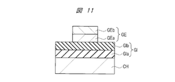
- FIG. 1 is a cross-sectional view showing the configuration of the semiconductor device of this embodiment.
- the semiconductor device shown in FIG. 1 is an MIS (Metal Insulator Semiconductor) type field effect transistor (FET) using a nitride semiconductor.
- FIG. 1 is a diagram schematically showing a configuration of a rectangular portion surrounded by a broken line in FIG. 2, for example.
- FIG. 2 is a cross-sectional view showing another configuration of the semiconductor device of the present embodiment. A semiconductor device as shown in FIG. 2 will be described in detail in a second embodiment.
- FIG. 3 is a cross-sectional view showing a configuration of Comparative Example 1 of the semiconductor device of the present embodiment.
- FIG. 4 is a cross-sectional view showing a configuration of Comparative Example 2 of the semiconductor device of the present embodiment.
- the semiconductor device of the present embodiment includes a gate electrode GE disposed on a channel layer CH made of a nitride semiconductor via a gate insulating film GI.
- the gate insulating film GI includes a first gate insulating film GIa formed on the channel layer CH and a second gate insulating film GIb formed on the first gate insulating film GIa.
- the gate electrode GE includes a first gate electrode GEa formed on the second gate insulating film GIb and a second gate electrode GEb formed on the first gate electrode GEa.
- the gate insulating film GI (GIa, GIb) and the gate electrode GE (GEa, GEb) will be described.
- the gate insulating film GI includes the first gate insulating film GIa formed on the channel layer CH and the second gate insulating film GIb formed on the first gate insulating film GIa.
- the first gate insulating film GIa is made of an oxide of a first metal (an oxide containing the first metal, an oxide film of the first metal).
- the second gate insulating film GIb is made of a second metal oxide (an oxide containing a second metal, a second metal oxide film). The electronegativity of the second metal is lower than the electronegativity of the first metal.
- the first gate insulating film GIa is not a film formed by thermally oxidizing the channel layer (nitride semiconductor) CH, but a film formed by a so-called deposition method (deposition method).
- the first metal is, for example, aluminum (Al).
- the oxide of the first metal is aluminum oxide (Al 2 O 3 ).
- the second metal is one or more elements selected from the group of Hf, Zr, Ta, Ti, Nb, La, Y, and Mg.
- the oxide of the second metal is, for example, hafnium oxide (HfO 2 ), zirconium oxide (ZrO 2 ), tantalum oxide (Ta 2 O 5 ), titanium oxide (TiO 2 ), niobium oxide (Nb 2 O 5). ), Lanthanum oxide (La 2 O 3 ), yttrium oxide (Y 2 O 3 ), and magnesium oxide (MgO).
- the composition ratio of the second metal and oxygen is not limited to the above. Moreover, you may contain 2 or more types of elements as a 2nd metal.
- both of the two or more elements must be lower than the electronegativity of the first metal.
- the metal having an impurity level may be contained regardless of the degree of electronegativity.
- the gate electrode GE includes the first gate electrode GEa formed on the second gate insulating film GIb and the second gate electrode GEb formed on the first gate electrode GEa.
- the first gate electrode GEa is a nitride of a third metal.
- Ti, Ta, W, etc. can be used as the third metal.
- the nitride of the third metal (nitride including the third metal, nitride film of the third metal) is TiN, TaN, or WN.
- the third metal a metal having conductivity, high workability, and low oxygen absorption and supply is preferable. In this respect, Ti is preferably used as the third metal.
- the second gate electrode GEb is made of a fourth metal.
- W As the fourth metal, W, Ru, or Ir can be used.
- the fourth metal is preferably one that has conductivity even after oxidation, has high workability, and blocks oxygen from entering the lower first gate electrode GEa. In this respect, it is preferable to use W as the fourth metal.
- the oxides of the first metal and the second metal having different electronegativity are stacked and used, and the oxide film of the second metal having a low electronegativity is disposed on the upper layer.
- the threshold voltage (Vth) can be positive (Vth> 0) (stacking effect of the gate insulating film).
- the nitride containing the third metal and the fourth metal are used as the gate electrode GE and the fourth metal is disposed in the upper layer, the diffusion of oxygen into the gate insulating film GI is prevented, and the threshold voltage ( Vth) can be reduced. In particular, even after an annealing process described later, the diffusion of oxygen can be reduced and the stacking effect of the gate insulating film can be maintained.
- N / M which is the ratio (stoichiometry) of the third metal (M) and nitrogen (N)
- N / M which is the ratio (stoichiometry) of the third metal (M) and nitrogen (N)
- N / M which is the ratio (stoichiometry ratio) of the third metal (M) and nitrogen (N)
- the ratio of the third metal (M) and nitrogen (N) can be measured by, for example, XPS (X-ray Photoelectron Spectroscopy).
- TiN film titanium nitride film
- MN film third metal nitride film
- the ratio of Ti / N of TiN is about 1.2 at maximum. Is possible. Therefore, it is preferable that 1 ⁇ N / Ti ⁇ 1.2.
- the thickness of the fourth metal is preferably 50 nm or more. As described above, the fourth metal has a role of preventing diffusion of oxygen from the surface of the gate electrode GE to the first gate electrode GEa. If a fourth metal (second gate electrode GEb) having a thickness of about 50 nm is stacked on the first gate electrode GEa, the oxygen concentration on the surface of the gate electrode GE is about one digit on the surface of the first gate electrode GEa. Can be lowered. For this reason, the diffusion of oxygen to the first gate electrode GEa can be effectively suppressed by setting the thickness of the fourth metal (for example, tungsten film (W film)) to 50 nm or more.
- W film tungsten film
- the threshold voltage (Vth) is negative (Vth ⁇ 0).
- Vth ⁇ 0 When the threshold voltage (Vth) becomes negative (Vth ⁇ 0), a normally-on state occurs.
- Al 2 O 3 aluminum oxide
- the second gate insulating film GIb in the upper layer is used.
- the threshold voltage (Vth) can be positive (Vth> 0) because Hf has a lower electronegativity than Al (stacking effect of the gate insulating film).
- heat treatment also referred to as annealing, annealing treatment, post-annealing, and recovery annealing
- the threshold voltage (Vth) is reduced by performing heat treatment after forming a layer (for example, a gate electrode or a wiring (including a source electrode and a drain electrode)) above the gate insulating film (Al 2 O 3 and HfO 2 ). It can be raised again to be positive (Vth> 0).
- the inventor diligently studied the cause of the variation in the degree of recovery of the flat band Vfb, and used the semiconductor device of Comparative Example 2 (FIG. 4) as one of experiments for pursuing the cause.
- the following experiment was conducted.
- the upper gate electrode GE one in which Au was formed by resistance heating vacuum deposition was prepared.
- a first gate insulating film GIa and a second gate insulating film GIb are stacked, annealed in an atmosphere of only an inert gas, and Au is resistance heating vacuum deposition as the gate electrode GE on the gate insulating film GI. What was formed by the method was produced. Note that a gate electrode was formed using a metal mask (shadow mask) during the deposition of Au. According to such Au deposition, the influence of charge-up damage can be avoided, and the influence of oxygen in the annealing atmosphere can be verified.
- oxygen in the annealing atmosphere destroys or reduces the polarization of oxygen formed at the interface between the first gate insulating film GIa and the second gate insulating film GIb. It has been found that the shift effect of the flat band Vfb based on the polarization effect is reduced.
- TiN when TiN is used for the gate electrode GE, once the film is formed, it is once taken out into the air and annealed, so that oxygen that has entered the TiN film or oxygen adsorbed on the surface of the TiN film is in the film Will spread. In addition, water molecules that have entered the TiN film also diffuse into the film. It is considered that oxygen (oxygen element) diffused in such a TiN film breaks the polarization formed in the gate insulating film and eliminates the effect of this polarization.
- a nitride containing a third metal and a fourth metal are stacked as the gate electrode GE, and the fourth metal is disposed in the upper layer. Therefore, it is possible to prevent the diffusion of oxygen into the gate insulating film GI, maintain the oxygen polarization (the gate insulating film stacking effect), and maintain the shift effect of the flat band Vfb.
- the threshold voltage (Vth) can be positive (Vth> 0).
- variation in threshold voltage (Vth) can be corrected.
- an annealing process for example, a heat treatment at 500 ° C. or higher
- TiN (as) a TiN film was formed on a Si substrate by a sputtering method.
- Sample 2 TiN (anneal)
- TiN (anneal) a TiN film was formed on a Si substrate by a sputtering method, and this TiN film was annealed under conditions equivalent to the recovery annealing.
- sample 3 W / TiN (as)
- a TiN film was formed on a Si substrate by a sputtering method, and a W film was continuously formed on the TiN film.
- Sample 4 TiN (anneal)
- TiN (anneal) a TiN film is formed on a Si substrate by a sputtering method, and a W film is continuously formed on the TiN film.
- Annealing was performed under conditions equivalent to the recovery annealing.
- FIG. 5 shows the oxygen concentration distribution in each sample.
- FIG. 5 (a) shows a graph of oxygen concentrations of four samples (samples 1 to 4).
- FIG. 5 (b) shows only the graphs of samples 1 and 2, and
- FIG. ) Describes only the graphs of Samples 3 and 4.
- the horizontal axis in FIG. 5 is the depth (Depth, [nm]), and the vertical axis is the oxygen concentration (Oxygen concentration, [atoms / cm 3 ]).
- 1.0E + 17 indicates 1.0 ⁇ 10 17 .
- the starting point of the depth is represented by being shifted by the thickness of the W film (about 90 nm).
- the peak confirmed at the position of 120 nm deep that is, the position corresponding to the boundary between the TiN film and the Si substrate is due to the natural oxide film on the Si substrate.
- the oxygen concentration in the TiN film is higher in the sample 2 (TiN (anneal)) than in the sample 1 (TiN (as)) (see the arrow a part).
- the oxygen concentration in the W film is high.
- the graphs of samples 3 and 4 overlap, and an increase in oxygen concentration could not be confirmed.
- the oxygen concentration on the surface of the TiN film is suppressed to be lower than in the case of the samples 1 and 2.
- oxygen and water molecules adsorbed on the surface of the second gate electrode GEb are TiN films that are the first gate electrode GEa even after annealing. It turned out not to spread. Thereby, the shift effect of the flat band Vfb by the polarization formed in the gate insulating film GI can be maintained.
- the film thickness of the second gate electrode GEb for preventing the diffusion of oxygen into the TiN film which is the first gate electrode GEa will be examined.
- the thickness of the W film is about 50 nm and the oxygen concentration is decreased by one digit. If the oxygen concentration on the surface is reduced by an order of magnitude, it is considered that the diffusion of oxygen into the TiN film is considerably suppressed, so that the thickness of the second gate electrode GEb is considered to be sufficiently effective at about 50 nm.
- the TiN film is rich in nitrogen, that is, the ratio of Ti / N in the TiN film is made larger than 1, so that dangling bonds that can occur in the grain boundary are made of nitrogen (N). Can be passivated. Thereby, adsorption
- oxygen such as HfO 2 that is the second gate electrode GEb moves to the first gate electrode GEa, and oxygen vacancies (oxygen vacancies) exist in the second gate electrode GEb. appear. This oxygen vacancy has a positive charge and shifts the flat band Vfb negatively. Therefore, when the TiN film is rich in nitrogen, such a shift of the flat band Vfb to the negative side can be suppressed.
- FIGS. 6 to 11 are cross-sectional views showing the manufacturing steps of the semiconductor device of the present embodiment.
- a substrate on which a channel layer CH is formed is prepared.
- the channel layer CH is a nitride semiconductor layer, and for example, a gallium nitride layer (GaN layer) is used.
- GaN substrate may be used as the substrate, and this substrate may be used as the channel layer CH.
- a GaN layer may be formed on a support substrate such as a Si substrate.
- MOCVD Metal-Chemical-Vapor-Deposition
- the surface of the channel layer (i-GaN layer, GaN substrate) CH is cleaned using a diluted HCl solution or the like.
- the gate insulating film GI including the first gate insulating film GIa and the second gate insulating film GIb is formed on the channel layer CH.
- a first gate insulating film (first metal oxide film) GIa is formed on the channel layer CH.
- an aluminum oxide film (Al 2 O 3 film) is deposited as the first gate insulating film GIa by using a deposition method.
- a deposition method For example, trimethylaluminum (Al (CH 3 ) 3 , TMA) and H 2 O (oxidant) are used as source gases, and an aluminum oxide film having a film thickness of about 50 nm to 100 nm is used in an atmosphere of 400 ° C. using an ALD method.
- a film (Al 2 O 3 film) is deposited. According to the ALD method, it is possible to form a film having good controllability and covering property and good film quality.
- ozone (O 3 ) may be used as the oxidizing agent in addition to H 2 O.
- an aluminum oxide film (Al 2 O 3 film) may be formed by an oxygen plasma CVD method in addition to the ALD method.
- heat treatment is performed.
- heat treatment is performed at 750 ° C. for about 1 minute in a nitrogen (N 2 ) atmosphere.
- N 2 nitrogen
- the traps trap levels, defects
- the first gate insulating film GIa here, the aluminum oxide film
- the trap density in the film becomes high, and hysteresis of capacitance-voltage characteristics (CV characteristics) is often observed.
- the hysteresis of this CV characteristic is, for example, that the CV waveform measured while increasing the voltage from -10V to + 10V and the CV waveform measured while decreasing the voltage from +10 to -10V are not the same. Say that the waveforms do not overlap. For this reason, by performing heat treatment, the trap density can be reduced and the hysteresis can be improved.
- a hafnium oxide film (HfO 2 ) is formed on the first gate insulating film GIa (here, the aluminum oxide film) as, for example, a second gate insulating film (second metal oxide film) GIb. Film).
- a hafnium oxide film is deposited by a reactive sputtering method using a Hf metal target and a mixed gas of argon (Ar) and oxygen (O 2 ).
- the film thickness of the hafnium oxide film can be adjusted, for example, in the range of about 1 to 10 nm. However, according to the study of the present inventor, even with a film thickness of 2 to 3 nm, a sufficient flat band Vfb shift effect can be obtained by the aforementioned polarization of oxygen.
- the reactive sputtering method is a kind of PVD method.
- an ALD method or a CVD method may be used in addition to the PVD (Physical Vapor Deposition) method.
- heat treatment is performed.
- heat treatment is performed at 750 ° C. for about 1 minute in a nitrogen (N 2 ) atmosphere.
- N 2 nitrogen
- traps trap levels, defects
- the heat treatment after the formation of the first gate insulating film GIa (aluminum oxide film) and the heat treatment after the formation of the second gate insulating film GIb (hafnium oxide film) are performed separately.
- the heat treatment after the formation of the first gate insulating film GIa is omitted, and the heat treatment is collectively performed after the formation of the laminated film of the first gate insulating film GIa (aluminum oxide film) and the second gate insulating film GIb (hafnium oxide film). You may go.
- the gate insulating film GI having a laminated film of the first gate insulating film GIa (aluminum oxide film) and the second gate insulating film GIb (hafnium oxide film) is formed.
- the gate electrode GE is formed on the gate insulating film GI.
- a titanium nitride film TiN film
- a tungsten film W film
- a titanium nitride film of about 20 nm is deposited on the second gate insulating film GIb by a reactive sputtering method using a Ti metal target and a mixed gas of argon (Ar) and nitrogen (N 2 ). Subsequently, as shown in FIG.
- a tungsten film of about 100 nm is deposited on the first gate electrode GEa by a sputtering method using a W metal target and argon (Ar) gas. It is preferable to perform these steps continuously without exposing to air between the TiN film forming step and the W film forming step. By performing vacuum transfer between the TiN film forming apparatus and the W film forming apparatus, continuous film formation can be performed without exposure to air.
- a film forming method in addition to the PVD method such as the sputtering method, an ALD method or a CVD method may be used. Further, the formation of the second gate insulating film GIb is not limited to the PVD method.
- the amount of oxygen taken into the surface of the first gate electrode GEa can be reduced, and oxygen diffusion can be suppressed.
- oxygen polarization gate insulating film stacking effect
- the flat band Vfb shifting effect can be maintained.
- the thickness of the second gate electrode (W film) GEb is about 50 nm and the oxygen concentration is decreased by an order of magnitude. Therefore, the film thickness of the second gate electrode (W film) GEb. About 50 nm or more is preferable.
- the second gate electrode (W film) GEb is formed and then exposed to the atmosphere and heat treatment (recovery annealing) is performed in the subsequent steps, it is preferable to form a W film having a thickness of 100 nm or more. .
- the upper limit of the film thickness of the second gate electrode (W film) GEb is, for example, about 500 nm.
- This heat treatment is a heat treatment for reducing traps (trap levels, defects) in the gate insulating film (Al 2 O 3 and HfO 2 ) caused by plasma and charged particles during the formation of the gate electrode GE.
- the optimum temperature, time, etc. may be selected according to the PVD conditions (for example, power and time) of the first gate electrode GEa and the second gate electrode GEb. According to the study of the present inventor, the temperature is preferably 400 ° C. to 600 ° C. and the time is preferably 10 minutes to 60 minutes.
- an atmosphere of an inert gas such as nitrogen (N 2 ) is preferably used.
- the gate electrode GE (first gate electrode GEa) having a desired shape is formed by patterning (processing) the laminated film of the titanium nitride film and the tungsten film using a photolithography technique and an etching technique.
- the second gate electrode GEb covers the entire upper surface of the first gate electrode GEa.
- the lower gate insulating film GI may be etched when the gate electrode GE is etched. Moreover, you may perform the said heat processing after this patterning process.
- the gate electrode GE having a stacked film of the first gate electrode GEa and the second gate electrode GEb is formed.
- the material of the first gate electrode GEa for example, TaN, WN or the like that is easy to perform gate etching may be used, and for example, Ru or Ir may be used as the second gate electrode GEb.
- the first metal oxide film and the second metal oxide film having a lower electronegativity than the first metal are stacked and used as the gate insulating film.
- Vth can be shifted in the positive direction.
- the nitride containing the third metal and the fourth metal are used as the gate electrode GE and the fourth metal is disposed in the upper layer, the diffusion of oxygen to the gate insulating film GI is prevented, and the polarization of oxygen is prevented.
- the stacking effect of the gate insulating film can be maintained, and the shift effect of the flat band Vfb can be maintained.
- the threshold voltage (Vth) can be positive (Vth> 0).
- variation in threshold voltage (Vth) can be corrected. In particular, even when an annealing process is performed after the formation of the gate insulating film GI, oxygen diffusion due to the annealing process can be reduced, and the stacking effect of the gate insulating film can be maintained.
- the gate insulating film and the gate electrode can be used as part of the semiconductor device illustrated in FIG. 2 .
- the gate insulating film and the gate in this embodiment can be applied to other parts.
- the present invention may be applied to a type of semiconductor device. A part of such application examples will be described in Embodiment 2 and Embodiment 6 described later.
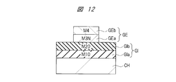
- FIG. 12 is a cross-sectional view showing a characteristic configuration of the semiconductor device of the present embodiment.
- the semiconductor device of the present embodiment has a gate electrode GE formed on a channel layer (nitride semiconductor) CH via a gate insulating film GI, as shown in FIG.
- the gate insulating film GI includes an oxide film M1O of the first metal M1 formed on the channel layer (nitride semiconductor) CH, and an oxide film M2O of the second metal M2 formed on the oxide film M1O. It goes without saying that the composition ratio of M1 and O and the composition ratio of M2 and O vary depending on the selected element.
- the electronegativity of the second metal M2 is smaller than the electronegativity of the first metal M1.
- the first metal M1 and the second metal M2 are selected from Group 2, Group 3, Group 4, Group 5, and Group 13 shown in Table 1 below (Pauling electronegativity).
- the oxide exists in a solid state at a device operating range temperature (for example, ⁇ 200 ° C.) and is a thin film and has good insulating properties.
- a combination of a lower oxide film and an upper oxide film may be selected from the relationship of electronegativity.
- the first metal M1 that is, the metal (element) constituting the lower oxide film
- Al is preferable.
- Si Group 14
- Si may be used as will be described in the third embodiment described later. If the surface of the nitride semiconductor is oxidized during the formation of the first metal oxide, an interface oxide layer having low insulating properties is formed, and the characteristics of the gate insulating film are impaired.
- the Al oxide that is, aluminum oxide, is suitable for use as a lower layer because it is difficult to form this interface reaction layer even if it is formed on a nitride semiconductor (particularly GaN).
- the gate electrode GE includes a nitride M3N of the third metal M3 formed on the gate insulating film GI and a fourth metal M4 formed on the nitride M3N of the third metal M3.
- the metals (M3, M3N, M4) suitable for use in this embodiment described above are summarized in Table 2 below.
- the composition ratio of N and M3, N / M3, is preferably larger than 1.
- the film thickness of M4 is preferably 50 nm or more.
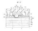
- FIG. 13 is a cross-sectional view showing the configuration of the semiconductor device of this embodiment.
- the semiconductor device shown in FIG. 13 is a MISFET using a nitride semiconductor. This semiconductor device is also called a high electron mobility transistor (HEMT) or a power transistor.
- the semiconductor device of this embodiment is a so-called recess gate type semiconductor device.
- the semiconductor device of the present embodiment has a plurality of nitride semiconductor layers formed on the substrate S. Specifically, a nucleation layer NUC, a strain relaxation layer STR, a buffer layer BU, a channel layer (also referred to as an electron transit layer) CH, and a barrier layer BA are sequentially formed on the substrate S.
- the gate electrode GE is formed through a gate insulating film GI in a trench (also referred to as a trench or a recess) T that penetrates the insulating film IF and the barrier layer BA and is dug in the middle of the channel layer CH.
- the gate insulating film GI includes a first gate insulating film GIa formed on the channel layer CH and a second gate insulating film GIb formed on the first gate insulating film GIa.
- the gate insulating film (first gate insulating film GIa, second gate insulating film GIb) described in 1 is made of the same material. That is, the first gate insulating film GIa is made of an oxide of the first metal.
- the second gate insulating film GIb is made of a second metal oxide. The electronegativity of the second metal is lower than the electronegativity of the first metal.
- the first gate insulating film GIa is not a film formed by thermally oxidizing the channel layer (nitride semiconductor) CH, but a film formed by a so-called deposition method (deposition method). That is, the lower oxide film of the first metal is not an oxide of an element constituting the nitride semiconductor layer. Thus, since the oxide film of the first metal is not formed by direct oxidation of the channel layer (nitride semiconductor), the first metal is different from the element constituting the channel layer (nitride semiconductor).
- the gate electrode GE includes the first gate electrode GEa formed on the channel layer CH and the second gate electrode GEb formed on the first gate electrode GEa, and the gate described in the first embodiment. It consists of the same material as an electrode (1st gate electrode GEa, 2nd gate electrode GEb). That is, the first gate electrode GEa is made of a nitride of a third metal (a nitride containing a third metal, a nitride film of a third metal).
- the second gate electrode GEb is made of a fourth metal.
- the composition ratio N / M3 of nitrogen (N) and third metal (M3) of the third metal nitride is preferably larger than 1.
- the film thickness of the fourth metal is preferably 50 nm or more.
- the source electrode SE and the drain electrode DE are formed on the barrier layer BA on both sides of the gate electrode GE.
- the nucleation layer NUC is formed on the substrate S, and the strain relaxation layer STR is formed on the nucleation layer NUC.
- the nucleation layer NUC is formed in order to generate crystal nuclei when a layer formed on the strain relaxation layer STR or the like grows. Further, it is formed to prevent the constituent elements (for example, Ga, etc.) of the layer formed in the upper part from diffusing from the layer formed in the upper part into the substrate S to change the quality of the substrate S.
- the strain relaxation layer STR is formed in order to relieve stress on the substrate S and suppress the occurrence of warpage and cracks in the substrate S.
- a buffer layer BU is formed on the strain relaxation layer STR, a channel layer (also referred to as an electron transit layer) CH made of a nitride semiconductor is formed on the buffer layer BU, and a nitride semiconductor is formed on the channel layer CH.
- a barrier layer BA is formed.
- a source electrode SE and a drain electrode DE are formed on the barrier layer BA on both sides of the gate electrode GE.
- the source electrode SE and drain electrode DE and the barrier layer BA are ohmically connected to each other.
- An insulating layer IL1 is formed over the gate electrode GE, and the insulating layer IL1 in the formation region of the source electrode SE and the drain electrode DE in the insulating layer IL1 is removed to form a contact hole. . Inside the contact hole, a conductive film is embedded, and the source electrode SE and the drain electrode DE are constituted by the conductive film.
- an insulating layer IL2 is formed on the source electrode SE and the drain electrode DE.
- the two-dimensional electron gas 2DEG is generated on the channel layer side near the interface between the channel layer CH and the barrier layer BA.
- a positive voltage threshold voltage
- a channel is formed in the vicinity of the interface between the gate electrode GE and the channel layer CH.
- the 2D electron gas 2DEG is formed by the following mechanism.
- Nitride semiconductors here, gallium nitride-based semiconductors
- the channel layer CH and the barrier layer BA have different forbidden bandwidths (band gaps) and electron affinities, respectively. For this reason, a well-type potential is generated at the junction surface of these semiconductors. By accumulating electrons in the well-type potential, a two-dimensional electron gas 2DEG is generated in the vicinity of the interface between the channel layer CH and the barrier layer BA.
- the two-dimensional electron gas 2DEG formed in the vicinity of the interface between the channel layer CH and the barrier layer BA is divided by the groove T in which the gate electrode GE is formed. For this reason, in the semiconductor device of this embodiment, on / off can be switched depending on whether or not a channel is formed.
- the gate insulating film GI since the stacked film of the first metal oxide and the second metal oxide having a lower electronegativity than the first metal disposed thereon is used as the gate insulating film GI.
- the flat band voltage (Vfb) can be shifted in the positive direction.
- the threshold voltage (Vth) can be shifted in the positive direction.
- the threshold voltage (Vth) can be positive (Vth> 0), and the normally-off characteristic can be improved.
- the gate electrode GE is exposed to the gate insulating film GI as in the first embodiment. Oxygen diffusion can be prevented and variation in threshold voltage (Vth) can be reduced. In particular, even after an annealing process described later, the diffusion of oxygen can be reduced and the stacking effect of the gate insulating film can be maintained.
- Vth threshold voltage
- N / M3 the same effect as in the first embodiment can be obtained.
- the effect similar to Embodiment 1 can be show
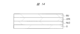
- FIGS. 14 to 25 are cross-sectional views showing the manufacturing process of the semiconductor device of the present embodiment.
- a semiconductor substrate made of silicon (Si) with an exposed (111) plane is used as the substrate S, and a nucleation layer NUC is formed on the semiconductor substrate, for example, aluminum nitride (AlN).
- the layer is heteroepitaxially grown using a metal organic chemical vapor deposition method or the like.
- a superlattice structure in which a laminated film (AlN / GaN film) of a gallium nitride (GaN) layer and an aluminum nitride (AlN) layer is repeatedly laminated is formed on the nucleation layer NUC as a strain relaxation layer STR. .
- a gallium nitride (GaN) layer and an aluminum nitride (AlN) layer are repeatedly heterogeneous by about 100 layers (total 200 layers) each with a thickness of about 2 to 3 nm using metal organic vapor phase epitaxy. Epitaxially grow.
- a substrate made of SiC, sapphire, or the like may be used in addition to the silicon.
- the buffer layer BU is formed on the strain relaxation layer STR.
- the buffer layer BU for example, an AlGaN layer is heteroepitaxially grown using a metal organic chemical vapor deposition method or the like.
- a channel layer CH is formed on the buffer layer BU.
- a gallium nitride layer i-GaN layer
- the electron affinity of the channel layer CH is larger than the electron affinity of the buffer layer BU.
- the channel layer CH is a nitride semiconductor having a narrower band gap than the buffer layer BU.
- barrier layer BA for example, an AlGaN layer is heteroepitaxially grown on the channel layer CH using a metal organic chemical vapor deposition method or the like.
- the electron affinity of the barrier layer BA is smaller than the electron affinity of the channel layer CH.
- the barrier layer BA is a nitride semiconductor having a wider band gap than the channel layer CH.
- a stacked body of the buffer layer BU, the channel layer CH, and the barrier layer BA is formed.
- This stacked body is formed by the above-described heteroepitaxial growth, that is, group III surface growth that is stacked in the [0001] crystal axis (C-axis) direction.
- the stacked body is formed by (0001) Ga surface growth.
- a two-dimensional electron gas 2DEG is generated near the interface between the channel layer CH and the barrier layer BA.
- an insulating film IF having an opening is formed on the barrier layer BA.
- a silicon nitride film is deposited on the barrier layer BA by using a thermal CVD method or the like.
- an opening is formed in the insulating film IF by using a photolithography technique and an etching technique.
- the barrier layer BA and the channel layer CH are etched to form a trench T that penetrates the insulating film IF and the barrier layer BA and reaches the middle of the channel layer CH (FIG. 17). After this etching, heat treatment may be performed to recover etching damage.
- the gate insulating film GI including the first gate insulating film GIa and the second gate insulating film GIb is formed in the trench T and on the insulating film IF.
- the first gate insulating film GIa is formed in the trench T where the channel layer CH is exposed at the bottom and on the insulating film IF.
- an aluminum oxide film Al 2 O 3 film
- Al 2 O 3 film is deposited on the bottom surface, the side wall, and the insulating film IF of the trench T (FIG. 18).
- a diluted HCl solution for example, trimethylaluminum (Al (CH 3 ) 3 , TMA) and H 2 O (oxidant) are used as source gases and an atmosphere at 400 ° C.
- an ALD method is used to deposit an aluminum oxide film (Al 2 O 3 film) having a thickness of about 50 nm to 100 nm in the trench T and on the insulating film IF.
- the film thickness can be controlled well, and a film can be formed on the uneven surface with good coverage.
- ozone (O 3 ) may be used as the oxidizing agent in addition to H 2 O.
- heat treatment is performed.
- heat treatment is performed at 750 ° C. for about 1 minute in a nitrogen (N 2 ) atmosphere.
- N 2 nitrogen
- traps trap levels, defects
- the first gate insulating film GIa here, the aluminum oxide film
- the trap density in the film increases and the hysteresis of the CV characteristic increases. For this reason, trap density can be reduced by performing heat treatment.
- a hafnium oxide film (HfO 2 film) is formed as the second gate insulating film GIb on the first gate insulating film GIa (here, the aluminum oxide film).
- a hafnium oxide film is deposited by a reactive sputtering method using a Hf metal target and a mixed gas of argon (Ar) and oxygen (O 2 ).
- the thickness of the hafnium oxide film varies depending on the threshold voltage (Vth), but is preferably about 1 to 10 nm.
- the reactive sputtering method is a kind of PVD method.
- an ALD method or a CVD method may be used.
- heat treatment is performed.
- heat treatment is performed at 750 ° C. for about 1 minute in a nitrogen (N 2 ) atmosphere.
- N 2 nitrogen
- traps trap levels, defects
- the heat treatment after the formation of the first gate insulating film GIa (aluminum oxide film) and the heat treatment after the formation of the second gate insulating film GIb (hafnium oxide film) are performed separately.
- the heat treatment after the formation of the first gate insulating film GIa is omitted, and the heat treatment is collectively performed after the formation of the laminated film of the first gate insulating film GIa (aluminum oxide film) and the second gate insulating film GIb (hafnium oxide film). You may go.
- the gate insulating film GI having a laminated film of the first gate insulating film GIa (aluminum oxide film) and the second gate insulating film GIb (hafnium oxide film) is formed.
- a gate electrode GE is formed on the gate insulating film GI.
- a titanium nitride film TiN film
- a tungsten film W film
- These laminated films are continuously formed using a multiter gate sputtering apparatus.
- a titanium nitride film of about 20 nm is deposited on the second gate insulating film GIb by a reactive sputtering method using a Ti metal target and a mixed gas of argon (Ar) and nitrogen (N 2 ).
- N / Ti which is a ratio of N to Ti of the formed TiN film, is set larger than 1.
- the ratio of N in the TiN film can be controlled by adjusting the amount of nitrogen in the mixed gas of argon (Ar) and nitrogen (N 2 ).
- a tungsten film having a thickness of about 100 nm is deposited on the first gate electrode GEa by a sputtering method using a W metal target and argon (Ar) gas.
- This heat treatment is a heat treatment for reducing traps (trap levels, defects) in the gate insulating film (Al 2 O 3 and HfO 2 ) caused by plasma and charged particles during the formation of the gate electrode GE.
- the optimum temperature, time, etc. may be selected according to the PVD conditions (for example, power and time) of the first gate electrode GEa and the second gate electrode GEb. According to the study of the present inventor, the temperature is preferably 400 ° C. to 600 ° C. and the time is preferably 10 minutes to 60 minutes.
- an atmosphere of an inert gas such as nitrogen (N 2 ) is preferably used.
- the gate electrode GE is formed by patterning the laminated film of the titanium nitride film and the tungsten film using the photolithography technique and the etching technique.
- the gate electrode GE is etched, the lower gate insulating film GI is also etched. Note that the heat treatment may be performed after the patterning step.
- the gate electrode GE having a stacked film of the first gate electrode GEa and the second gate electrode GEb is formed.
- the material of the first gate electrode GEa for example, TaN, WN or the like that is easy to perform gate etching may be used, and for example, Ru or Ir may be used as the second gate electrode GEb.
- a silicon oxide film is formed as the insulating layer IL1 over the gate electrode GE and the insulating film IF by using a CVD method or the like.
- the insulating layer IL1 and the insulating film IF over the source electrode SE formation region and the drain electrode DE formation region are removed by etching, and contact is performed.
- a hole is formed.
- the source electrode SE and the drain electrode DE are formed on the barrier layer BA on both sides of the gate electrode GE.
- a conductive film is formed over the insulating layer IL1 including the inside of the contact hole.
- a laminated film (Al / TiN) including a titanium nitride (TiN) film and an aluminum (Al) film thereon is formed by a sputtering method or the like.
- the stacked film (Al / TiN) is patterned by using a photolithography technique and an etching technique, and a heat treatment is performed at 550 ° C. for about 30 minutes, for example.
- a heat treatment is performed at the interface between the source electrode SE and drain electrode DE and the barrier layer BA (nitride semiconductor film) becomes ohmic contact.
- an insulating layer (also referred to as a cover film or a surface protective film) IL2 is formed on the insulating layer IL1 including the source electrode SE and the drain electrode DE.
- a silicon oxynitride (SiON) film is deposited using a CVD method or the like (FIG. 25).
- the semiconductor device of this embodiment can be formed.
- the first metal oxide film and the second metal oxide film having a lower electronegativity than the first metal are stacked, and the gate is formed.
- the threshold voltage (Vth) can be shifted in the positive direction. Then, by adjusting the shift amount, it is possible to realize normally-off in which the threshold voltage (Vth) is positive (Vth> 0).
- the nitride containing the third metal and the fourth metal are used as the gate electrode GE and the fourth metal is disposed in the upper layer, the diffusion of oxygen to the gate insulating film GI is prevented, and the polarization of oxygen is prevented.
- the stacking effect of the gate insulating film can be maintained, and the shift effect of the flat band Vfb can be maintained.
- the threshold voltage (Vth) can be positive (Vth> 0).
- variation in threshold voltage (Vth) can be corrected. In particular, even when an annealing process is performed after the formation of the gate insulating film GI, oxygen diffusion due to the annealing process can be reduced, and the stacking effect of the gate insulating film can be maintained.
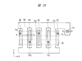
- FIG. 26 is an example of a plan view showing the configuration of the semiconductor device of this embodiment.
- FIG. 13 corresponds to the AA cross section of FIG.
- the source electrode SE and the drain electrode DE are, for example, in a line shape extending in the Y direction. In other words, it is a rectangular shape (rectangular shape) having long sides in the Y direction.
- the source electrode SE and the drain electrode DE are alternately arranged in the X direction.
- the gate electrode GE is disposed between the source electrode SE and the drain electrode DE.
- one end (upper side in the drawing) of the plurality of line-shaped gate electrodes (GE) extending in the Y direction is connected to a line (also referred to as a gate line) extending in the X direction.
- the other end (lower side in the figure) of the plurality of line-shaped gate electrodes (GE) extending in the Y direction is connected to a line (also referred to as a gate line) extending in the X direction.
- a line also referred to as a gate line
- one of the two lines (also referred to as gate lines) extending in the X direction may be omitted, and the gate electrode GE may have a comb shape.
- the plurality of source electrodes SE are connected to a source line SL extending in the X direction via a plug (connection portion) PG.
- the plurality of drain electrodes DE are connected to a drain line DL extending in the X direction via a plug (connection portion) PG.
- the source electrode SE and the source line SL may be arranged in the same layer.
- a shape (comb shape) in which a line extending in the X direction (corresponding to the source line portion) and a line-shaped source electrode extending in the Y direction may be connected.
- the drain electrode DE and the drain line DL may be arranged in the same layer.
- a shape (comb shape) in which a line extending in the X direction (corresponding to the drain line portion) and a line-shaped drain electrode extending in the Y direction may be connected.
- the layout of the gate electrode GE, the source electrode SE, the drain electrode DE, and other wirings can be changed as appropriate, and the number of wiring layers is not limited.
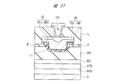
- FIG. 27 is a cross-sectional view showing the configuration of the semiconductor device of this embodiment.
- FIG. 27 corresponds to, for example, the BB cross section of FIG.
- the plug PG is made of, for example, an Al / TiN film.
- the oxide film (GIa) below the gate insulating film GI is the first metal oxide film.
- the oxide film below this oxide film may be a silicon oxide film. That is, Si (semiconductor) is used as an element constituting the lower oxide film.
- FIG. 28 is a cross-sectional view showing a configuration of the semiconductor device of the present embodiment.
- the semiconductor device of this embodiment is the same as that of Embodiment 1 except that the first gate insulating film GIa is a silicon oxide film.
- the gate electrode GE disposed on the channel layer CH made of a nitride semiconductor via the gate insulating film GI. (GEa, GEb).
- the gate insulating film GI includes a silicon oxide film (SiO 2 ) that is the first gate insulating film GIa formed on the channel layer CH, and a second gate insulating film formed on the first gate insulating film GIa.
- the gate electrode GE includes a first gate electrode GEa formed on the second gate insulating film GIb and a second gate electrode GEb formed on the first gate electrode GEa.
- a silicon oxide film (SiO 2 ) is provided as the first gate insulating film GIa.
- an oxide film of a second metal (M2) is provided as the second gate insulating film GIb.
- the second metal is one or more elements selected from the group consisting of Al, Hf, Zr, Ta, Ti, Nb, La, Y, and Mg.
- the oxide of the second metal is, for example, aluminum oxide (Al 2 O 3 ), hafnium oxide (HfO 2 ), zirconium oxide (ZrO 2 ), tantalum oxide (Ta 2 O 5 ), titanium oxide (TiO 2 ). ), Niobium oxide (Nb 2 O 5 ), lanthanum oxide (La 2 O 3 ), yttrium oxide (Y 2 O 3 ), and magnesium oxide (MgO).
- the electronegativity of the elements (Si, M2) constituting the two-layer gate insulating films (GIa, GIb) is Si> M2. Also in this case, the oxygen polarization effect described in Embodiment 1 occurs, and the flat band Vfb shifts in the positive direction.
- the gate electrode GE has a stacked structure, that is, a structure in which a nitride including the third metal and the fourth metal are stacked and the fourth metal is disposed in the upper layer.
- a stacked structure that is, a structure in which a nitride including the third metal and the fourth metal are stacked and the fourth metal is disposed in the upper layer.
- the manufacturing method of the semiconductor device of the present embodiment is the same as that of the first embodiment except for the step of forming the gate insulating film GI.
- a silicon oxide film (SiO 2 ) is formed on the channel layer CH as the first gate insulating film GIa. Film) is deposited using a deposition method.
- a film having a thickness of about 3 nm is formed using trisdimethylaminosilane (SiH (N (CH 3 ) 2 ) 3 , TDMAS) and ozone (O 3 , oxidizing agent) as source gases and using an ALD method in an atmosphere of 480 ° C.
- a thick silicon oxide film (SiO 2 film) is deposited.
- the film thickness of the silicon oxide film can be adjusted, for example, in the range of 3 nm to 20 nm.
- a silicon oxide film may be deposited using a CVD method (thermal CVD, plasma CVD method, or the like). According to the study of the present inventor, even with a film thickness of about 3 to 5 nm, a sufficient flat band Vfb shift effect can be obtained by the aforementioned oxygen polarization.
- heat treatment is performed.
- heat treatment is performed at 750 ° C. for about 1 minute in a nitrogen (N 2 ) atmosphere.
- N 2 nitrogen
- a second gate insulating film (second metal oxide film) GIb is formed on the first gate insulating film GIa.
- an aluminum oxide film (Al 2 O 3 film) having a thickness of about 50 nm to 100 nm is deposited as the second gate insulating film GIb.
- heat treatment is performed.
- heat treatment is performed at 750 ° C. for about 1 minute in a nitrogen (N 2 ) atmosphere.
- N 2 nitrogen
- the heat treatment is individually performed after the formation of each gate insulating film (GIa, GIb).
- the heat treatment may be collectively performed after the formation of the second gate insulating film GIb.
- the gate insulating film GI can be formed in which the first gate insulating film GIa (silicon oxide film) and the second gate insulating film GIb (aluminum oxide film) are sequentially stacked from the bottom.
- a gate electrode GE (GEa, GEb) is formed on the gate insulating film GI.
- gate insulating film GI of the present embodiment may be used as the gate insulating film GI of the second embodiment.
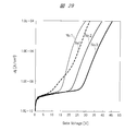
- FIG. 29 is a graph showing the stacking effect of the gate insulating film.
- the horizontal axis represents the gate voltage (Gate Voltage [V]), and the vertical axis represents the current (Jg [A / cm 2 ]).
- V Gate Voltage
- Jg Jg [A / cm 2 ]
- the gate electrode was a single layer. Ref, No. 1, no. 2, No. 3, a laminated film of Al 2 O 3 / SiO 2 was used, and the film thickness of SiO 2 was set to 0 nm, 3 nm, 5 nm, and 10 nm. No. 1, no. 2, No. 3, that is, when the film thickness of SiO 2 is 3 nm to 10 nm, the rising voltage of the current becomes high. This is considered to be due to the shift effect of the flat band Vfb and the withstand voltage improvement effect.
- the gate electrode laminated structure is added to the gate insulating film laminated structure, so that the shift effect of the flat band Vfb can be maintained, so that the rising voltage of the current can be maintained.
- the gate insulating film GI has two layers (GIa, GIb). However, the gate insulating film GI has three layers, and the first gate insulating film GIa and the second gate insulating film GIb A third gate insulating film (lowermost gate insulating film) GIu may be provided under the stacked film (substrate or channel layer side). And Si (semiconductor) is used as an element which comprises this 3rd gate insulating film (lowermost layer gate insulating film) GIu.
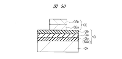
- FIG. 30 is a cross-sectional view showing the configuration of the semiconductor device of the present embodiment.
- the semiconductor device of the present embodiment is the same as that of the first embodiment except that the gate insulating film GI is composed of three layers.
- the gate electrode GE disposed on the channel layer CH made of a nitride semiconductor via the gate insulating film GI. (GEa, GEb).
- the gate insulating film GI includes a silicon oxide film (SiO 2 ) that is a third gate insulating film GIu formed on the channel layer CH, and a first gate insulating film formed on the third gate insulating film GIu.
- the first gate insulating film GIa is made of an oxide of the first metal.
- the second gate insulating film GIb is made of a second metal oxide.
- the electronegativity of the second metal is lower than the electronegativity of the first metal.
- the electronegativity of the first metal is lower than that of Si.
- the gate electrode GE includes the first gate electrode GEa formed on the channel layer CH and the second gate electrode GEb formed on the first gate electrode GEa, and the gate described in the first embodiment. It consists of the same material as an electrode (1st gate electrode GEa, 2nd gate electrode GEb). That is, the first gate electrode GEa is made of a nitride of a third metal (a nitride containing a third metal, a nitride film of a third metal).
- the second gate electrode GEb is made of a fourth metal.
- the composition ratio N / M3 of nitrogen (N) and third metal (M3) of the third metal nitride is preferably larger than 1.
- the film thickness of the fourth metal is preferably 50 nm or more.
- a silicon oxide film (SiO 2 ) is provided as the third gate insulating film (lowermost layer gate insulating film) GIu.
- the electronegativity of the elements (Si, M1, M2) constituting the three-layer gate insulating films (GIu, GIa, GIb) can be sequentially decreased from the lower layer side. Thereby, the effect of the polarization of oxygen described in the first embodiment is increased, and the shift amount of the flat band Vfb is increased.
- the gate electrode GE has a stacked structure, that is, a structure in which a nitride including the third metal and the fourth metal are stacked and the fourth metal is disposed in the upper layer.
- a stacked structure that is, a structure in which a nitride including the third metal and the fourth metal are stacked and the fourth metal is disposed in the upper layer.
- the manufacturing method of the semiconductor device of the present embodiment is the same as that of the first embodiment except for the step of forming the gate insulating film GI.
- the third gate insulating film (lowermost layer gate insulating film) GIu is formed on the channel layer CH. Then, a silicon oxide film (SiO 2 film) is deposited using a deposition method.
- a film having a thickness of about 3 nm is formed using trisdimethylaminosilane (SiH (N (CH 3 ) 2 ) 3 , TDMAS) and ozone (O 3 , oxidizing agent) as source gases and using an ALD method in an atmosphere of 480 ° C.
- a thick silicon oxide film (SiO 2 film) is deposited.
- the film thickness of the silicon oxide film can be adjusted, for example, in the range of 3 nm to 20 nm.
- a silicon oxide film may be deposited using a CVD method (thermal CVD, plasma CVD method, or the like). According to the study of the present inventor, even with a film thickness of about 3 to 5 nm, a sufficient flat band Vfb shift effect can be obtained by the aforementioned oxygen polarization.
- heat treatment is performed.
- heat treatment is performed at 750 ° C. for about 1 minute in a nitrogen (N 2 ) atmosphere.
- N 2 nitrogen
- a first gate insulating film (first metal oxide film) GIa is formed on the third gate insulating film GIu.
- first metal oxide film first metal oxide film
- Al 2 O 3 film aluminum oxide film
- heat treatment is performed.
- heat treatment is performed at 750 ° C. for about 1 minute in a nitrogen (N 2 ) atmosphere.
- N 2 nitrogen
- a second gate insulating film (second metal oxide film) GIb is formed on the first gate insulating film GIa.
- a hafnium oxide film (HfO 2 film) is deposited to a thickness of about 2 nm as the second gate insulating film GIb.
- heat treatment is performed.
- heat treatment is performed at 750 ° C. for about 1 minute in a nitrogen (N 2 ) atmosphere.
- N 2 nitrogen
- the heat treatment is individually performed after the formation of each gate insulating film (GIu, GIa, GIb).
- the heat treatment may be collectively performed after the formation of the second gate insulating film GIb.
- a film GI can be formed.
- a gate electrode GE (GEa, GEb) is formed on the gate insulating film GI.
- the three-layer gate insulating film GI of the present embodiment may be used as the gate insulating film GI of the second embodiment.
- the silicon oxide film is used as the third gate insulating film (lowermost gate insulating film) GIu.
- a silicon nitride film may be provided.
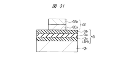
- FIG. 31 is a cross-sectional view showing the configuration of the semiconductor device of the present embodiment.
- the semiconductor device of the present embodiment is the same as that of the fourth embodiment except for the third gate insulating film (lowermost layer gate insulating film) GIu of the gate insulating film GI.
- the gate electrode GE disposed on the channel layer CH made of a nitride semiconductor via the gate insulating film GI. (GEa, GEb).
- the gate insulating film GI includes a silicon nitride film (SiN x ) that is the third gate insulating film GIu formed on the channel layer CH, and a first gate insulating film formed on the third gate insulating film GIu.
- the gate electrode GE includes a first gate electrode GEa formed on the second gate insulating film GIb and a second gate electrode GEb formed on the first gate electrode GEa.
- the silicon nitride film (SiN x ) is provided as the third gate insulating film (lowermost layer gate insulating film) GIu.
- the silicon nitride film (GIu) does not contain oxygen, no polarization of oxygen occurs at the interface between the first gate insulating film GIa and the interface between the first gate insulating film GIa and the second gate insulating film GIb.
- the flat band Vfb is shifted in the positive direction due to the generated polarization.
- the oxidation of the channel layer CH (here, i-GaN layer) can be suppressed.
- a nitride semiconductor such as a GaN layer
- many interface states are generated at the interface with the gate insulating film GI. In this case, the mobility of the MISFET decreases. This degrades the performance of the MISFET.
- oxidation annealing after film formation is effective.
- a nitride semiconductor such as a GaN layer is in contact with an oxide film, the oxidation of the nitride semiconductor may further progress due to oxidation annealing.
- the oxidation is suppressed.
- the oxidation of the nitride semiconductor due to contact with the gate insulating film GI can be suppressed. Even when oxidation annealing is performed, oxidation of the nitride semiconductor can be suppressed.
- the gate electrode GE has a stacked structure, that is, a structure in which a nitride including the third metal and the fourth metal are stacked and the fourth metal is disposed in the upper layer.
- a stacked structure that is, a structure in which a nitride including the third metal and the fourth metal are stacked and the fourth metal is disposed in the upper layer.
- the manufacturing method of the semiconductor device of the present embodiment is the same as that of the fourth embodiment except for the step of forming the third gate insulating film (lowermost layer gate insulating film) GIu.
- the third gate insulating film (lowermost layer gate insulating film) is formed on the channel layer CH.
- a silicon nitride film SiN X film is deposited using a deposition method.
- trisdimethylaminosilane (SiH (N (CH 3 ) 2 ) 3 , TDMAS) and ammonia (NH 3 ) are used as source gases and nitrided to a thickness of about 4 nm using an ALD method in an atmosphere of 480 ° C.
- a silicon film (SiN X film) is deposited.
- the film thickness of the silicon nitride film can be adjusted, for example, in the range of 1 nm to 15 nm.
- a silicon nitride film may be deposited by a CVD method (thermal CVD, plasma CVD method, or the like).
- heat treatment is performed.
- heat treatment is performed at 750 ° C. for about 1 minute in a nitrogen (N 2 ) atmosphere.
- N 2 nitrogen
- a first gate insulating film (first metal oxide film) GIa is formed on the third gate insulating film GIu.
- first metal oxide film first metal oxide film
- Al 2 O 3 film aluminum oxide film
- heat treatment is performed.
- heat treatment is performed at 750 ° C. for about 1 minute in a nitrogen (N 2 ) atmosphere.
- N 2 nitrogen
- a second gate insulating film (second metal oxide film) GIb is formed on the first gate insulating film GIa.
- a hafnium oxide film (HfO 2 film) is deposited to a thickness of about 2 nm as the second gate insulating film GIb.
- heat treatment is performed.
- heat treatment is performed at 750 ° C. for about 1 minute in a nitrogen (N 2 ) atmosphere.
- N 2 nitrogen
- the heat treatment is individually performed after the formation of each gate insulating film (GIu, GIa, GIb).
- the heat treatment may be collectively performed after the formation of the second gate insulating film GIb.
- a film GI can be formed.
- a gate electrode GE (GEa, GEb) is formed on the gate insulating film GI.
- the three-layer gate insulating film GI of the present embodiment may be used as the gate insulating film GI of the second embodiment.
- the nitride semiconductor (GaN layer) is used as the channel layer CH.
- other semiconductor layers may be used.
- an SiC layer SiC substrate is used.
- FIG. 32 is a cross-sectional view showing a configuration of the semiconductor device of the present embodiment.
- the semiconductor device of the present embodiment includes a gate electrode GE disposed on a channel layer CH made of SiC via a gate insulating film GI.
- the gate insulating film GI includes a first gate insulating film GIa formed on the channel layer CH and a second gate insulating film GIb formed on the first gate insulating film GIa.
- the gate electrode GE includes a first gate electrode GEa formed on the second gate insulating film GIb and a second gate electrode GEb formed on the first gate electrode GEa.
- An SiC layer may be provided as a channel layer CH on a substrate such as Si, or an SiC substrate may be used as the substrate, and this substrate may be used as the channel layer CH.
- a source region SR and a drain region DR which are n-type or p-type impurity implantation regions, are disposed. Further, a source electrode SE and a drain electrode DE are disposed on the source region SR and the drain region DR.
- the gate insulating film GI includes a first gate insulating film GIa formed on the channel layer CH and a second gate insulating film GIb formed on the first gate insulating film GIa.
- the first gate insulating film GIa is made of a silicon oxide film (SiO 2 ).
- the second gate insulating film GIb is made of a second metal oxide. The electronegativity of the second metal is lower than that of Si.
- the gate insulating film GI is a silicon oxide film (SiO 2 ) made of the first metal oxide of the gate insulating film GI of the first embodiment.
- the first gate insulating film (SiO 2 ) GIa may be a thermal oxide film of a channel layer (SiC layer) CH or may be a deposited film.
- the thermal oxidation method dry oxidation or wet oxidation can be used. Moreover, you may oxidize using ozone.
- As the deposition method an ALD method, a CVD method, or a PVD method may be used.
- the film thickness of the silicon oxide film can be adjusted in the range of 1 nm to 10 nm.
- the second metal is a metal lower than the electronegativity of Si, for example, aluminum (Al).
- the oxide of the first metal is aluminum oxide (Al 2 O 3 ).
- the film thickness of the first metal oxide is, for example, about 60 nm.
- the second metal in addition to Al, Hf, Zr, Ta, Ti, Nb, La, Y, Mg, or the like can be used.
- the oxide film in this case include hafnium oxide (HfO 2 ), zirconium oxide (ZrO 2 ), tantalum oxide (Ta 2 O 5 ), titanium oxide (TiO 2 ), niobium oxide (Nb 2 O 5 ), and lanthanum oxide. (La 2 O 3 ), yttrium oxide (Y 2 O 3 ), and magnesium oxide (MgO).
- the composition ratio of the second metal and oxygen is not limited to the above. Moreover, you may contain 2 or more types of elements as a 2nd metal.
- each of the first gate insulating film GIa and the second gate insulating film GIb depends on the characteristics required for the gate insulating film GI and the film quality (electric characteristics such as dielectric constant and leakage characteristics) resulting from the deposition method. A suitable combination can be selected.
- the gate electrode GE includes a first gate electrode GEa formed on the second gate insulating film GIb and a second gate electrode GEb formed on the first gate electrode GEa.
- the first gate electrode GEa is a nitride film containing a third metal.
- Ti, Ta, W, etc. can be used as the third metal.
- the nitride film containing the third metal is TiN, TaN, or WN.
- the third metal a metal having conductivity, high workability, and low oxygen absorption and supply is preferable. In this respect, Ti is preferably used as the third metal.
- the second gate electrode GEb is made of a fourth metal.
- W As the fourth metal, W, Ru, or Ir can be used.
- the fourth metal is preferably one that has conductivity even after oxidation, has high workability, and blocks oxygen from entering the lower first gate electrode GEa. In this respect, it is preferable to use W as the fourth metal.
- the gate insulating film GI is formed by stacking the oxides of Si and the second metal, and the second metal oxide film having an electronegativity lower than that of Si is disposed on the upper layer. Therefore, the threshold voltage (Vth) can be positive (Vth> 0) (a gate insulating film stacking effect).
- the nitride containing the third metal and the fourth metal are used as the gate electrode GE and the fourth metal is disposed in the upper layer, the diffusion of oxygen into the gate insulating film GI is prevented, and the threshold voltage ( Vth) can be reduced. In particular, even after an annealing process described later, the diffusion of oxygen can be reduced and the stacking effect of the gate insulating film can be maintained.
- the channel layer CH is a SiC layer.
- the SiC layer can be formed using, for example, a CVD method.
- a SiC substrate may be used as the substrate, and this substrate may be used as the channel layer CH.
- the surface of the channel layer (SiC layer) CH is washed using sulfuric acid / hydrogen peroxide solution or ammonia / hydrogen peroxide solution.
- the gate insulating film GI including the first gate insulating film GIa and the second gate insulating film GIb is formed on the channel layer CH.
- the first gate insulating film GIa is formed on the channel layer CH.
- a silicon oxide film SiO 2 film
- dry oxidation at an oxidation temperature of 1300 ° C. is performed in a mixed gas of O 2 and N 2 to form a silicon oxide film having a thickness of about 10 nm, for example.
- the oxidation method is not limited to dry oxidation, and thermal oxidation with other oxidizing agents may be used.
- the silicon oxide film may be formed using a deposition method such as a CVD method, an ALD method, or a PVD method.
- the interface (SiO 2 / SiC interface) between the first gate insulating film GIa and the channel layer CH is nitrided.
- nitriding treatment for example, heat treatment is performed at 1000 ° C. for 1 hour in an atmosphere containing nitric oxide (NO).
- NO nitric oxide
- interface states such as dangling bonds
- a gas used for this nitriding treatment N 2 O, NH 3 or the like may be used in addition to the above-mentioned nitric oxide (NO). Further, a mixed gas of these gases may be used. Further, a plurality of gases may be used while being switched every time.
- this nitriding treatment may cause not only a nitriding reaction but also an oxidation reaction (oxynitriding treatment).
- oxynitriding treatment an oxidation reaction
- a hydrogenation process or a V grouping process for example, phosphation
- the interface state can be reduced.
- a second gate insulating film (second metal oxide film) GIb is formed on the first gate insulating film (silicon oxide film) GIa.
- an aluminum oxide film (Al 2 O 3 film) is deposited as the second gate insulating film GIb using a deposition method.
- trimethylaluminum (Al (CH 3 ) 3 , TMA) and H 2 O (oxidant) are used as source gases, and an aluminum oxide film having a thickness of about 60 nm (400 nm) using an ALD method in an atmosphere of 400 ° C. Al 2 O 3 film) is deposited.
- the ALD method it is possible to form a film having good controllability and covering property and good film quality.
- ozone may be used as the oxidizing agent in addition to H 2 O.
- an aluminum oxide film (Al 2 O 3 film) may be formed by an oxygen plasma CVD method in addition to the ALD method.
- heat treatment is performed. For example, heat treatment is performed at 600 ° C. for about 30 minutes in a nitrogen (N 2 ) atmosphere.
- Al is used as the metal for the second gate insulating film GIb, but the second metal is, for example, selected from the group of Hf, Zr, Ta, Ti, Nb, La, Y, and Mg. Oxides of the above elements may be used.
- the gate insulating film GI having a laminated film of the first gate insulating film GIa (silicon oxide film) and the second gate insulating film GIb (aluminum oxide film) is formed.
- the gate electrode GE is formed over the gate insulating film GI.
- a titanium nitride film TiN film
- a tungsten film W film
- These laminated films are continuously formed using a multiter gate sputtering apparatus.
- a titanium nitride film of about 20 nm is deposited on the second gate insulating film GIb by a reactive sputtering method using a Ti metal target and a mixed gas of argon (Ar) and nitrogen (N 2 ).
- N / Ti which is a ratio of N to Ti of the formed TiN film, is set larger than 1.
- the proportion of N in TiN can be controlled by adjusting the amount of nitrogen in the mixed gas of argon (Ar) and nitrogen (N 2 ).
- a tungsten film having a thickness of about 100 nm is deposited on the first gate electrode GEa as the second gate electrode GEb by a sputtering method using a W metal target and argon (Ar) gas.
- the second gate electrode (W film) GEb has a thickness of about 50 nm and the oxygen concentration is decreased by one digit.
- the film thickness is preferably 50 nm or more.
- the second gate electrode (W film) GEb is formed and then exposed to the atmosphere and heat treatment (recovery annealing) is performed in the subsequent steps, it is preferable to form a W film having a thickness of 100 nm or more. .
- the upper limit of the film thickness of the second gate electrode (W film) GEb is, for example, about 500 nm.
- This heat treatment is a heat treatment for reducing traps (trap levels, defects) in the gate insulating film (Al 2 O 3 and HfO 2 ) caused by plasma and charged particles during the formation of the gate electrode GE.
- the optimum temperature, time, etc. may be selected according to the PVD conditions (for example, power and time) of the first gate electrode GEa and the second gate electrode GEb. According to the study of the present inventor, the temperature is preferably 400 ° C. to 600 ° C. and the time is preferably 10 minutes to 60 minutes.
- an atmosphere of an inert gas such as nitrogen (N 2 ) is preferably used.
- the gate electrode GE having a desired shape is formed by patterning (processing) the first gate electrode GEa and the second gate electrode GEb using a photolithography technique and an etching technique.
- the second gate electrode GEb covers the entire upper surface of the first gate electrode GEa.
- the lower gate insulating film GI may be etched when the gate electrode GE is etched.
- the material of the first gate electrode GEa for example, TaN, WN, or the like that is easy to perform gate etching may be used, and for example, Ru, Ir, or the like may be used as the second gate electrode GEb.
- an n-type or p-type impurity is implanted into the channel layer CH on both sides of the gate electrode GE, thereby forming the source region SR and the drain region DR.
- a silicon oxide film is formed as the insulating layer IL1 over the gate electrode GE, the source region SR, and the drain region DR by using a CVD method or the like.
- the insulating layer IL1 over the source region SR and the drain region DR is removed by etching to form a contact hole.
- the source electrode SE and the drain electrode DE are formed on the source region SR and the drain region DR on both sides of the gate electrode GE, respectively.
- a conductive film is formed over the insulating layer IL1 including the inside of the contact hole.
- the conductive film is patterned by using a photolithography technique and an etching technique.
- the source electrode SE and the drain electrode DE may be formed using a so-called damascene method.
- a plurality of wirings may be formed over the insulating layer IL1.
- the semiconductor device of this embodiment can be formed.
- the stacked film of the Si oxide and the second metal oxide having a lower electronegativity than Si disposed thereon is used as the gate insulating film GI.
- the flat band voltage (Vfb) can be shifted in the positive direction.
- the threshold voltage (Vth) can be shifted in the positive direction.
- the threshold voltage (Vth) can be positive (Vth> 0), and the normally-off characteristic can be improved.
- the gate electrode GE is exposed to the gate insulating film GI as in the first embodiment. Oxygen diffusion can be prevented and variation in threshold voltage (Vth) can be reduced. In particular, even after an annealing process described later, the diffusion of oxygen can be reduced and the stacking effect of the gate insulating film can be maintained.
- Vth threshold voltage
- N / M3 the same effect as in the first embodiment can be obtained.
- the SiC layer as the channel layer CH, the flat band Vfb is shifted in the positive direction, and the threshold voltage (Vth) is shifted in the positive direction, the impurity concentration for Vth control of the channel layer CH can be lowered.
- Impurities reduce the mobility of carriers (electrons or holes) traveling in the channel layer CH (impurity scattering). Therefore, by reducing the impurity concentration of the channel layer, carrier mobility is improved, and as a result, the on-current of the MISFET can be increased.
- the mobility depends on the crystal plane on which the MISFET is formed, the mobility improvement effect is useful because the mobility of the SiC layer is smaller than the mobility of the Si layer.
- a stacked film of a silicon oxide film and an aluminum oxide film (for example, corresponding to Embodiment 3) is used as the gate insulating film GI, but the other Embodiments 1, 4, 5 are used.
- the gate insulating film GI described in the above may be applied.
- [Appendix 1] A SiC layer; A first gate insulating film provided on the SiC layer; A second gate insulating film provided on the first gate insulating film; A first gate electrode provided on the second gate insulating film; A second gate electrode provided on the first gate electrode; Have The first gate insulating film is an oxide film containing a first metal or an oxide film containing silicon, The second gate insulating film is an oxide film containing a second metal; The electronegativity of the second metal is smaller than the electronegativity of the first metal or silicon, The first gate electrode is a nitride film containing a third metal; The semiconductor device, wherein the second gate electrode is made of a fourth metal.
- the nitride film containing the third metal is titanium nitride, The ratio of titanium (Ti) to nitrogen (N) (N / Ti) is greater than one.
- [Appendix 10] In the method for manufacturing a semiconductor device according to attachment 8, In the step (d) to the step (e), A method of manufacturing a semiconductor device, wherein after forming the first gate electrode, the second gate electrode is formed without being exposed to air.
- the first gate insulating film is made of an oxide film containing silicon
- the second metal is one or more elements selected from the group of Al, Hf, Zr, Ta, Ti, Nb, La, Y, Mg,
- the third metal is Ti;
- the method for manufacturing a semiconductor device, wherein the fourth metal is W.
- the first gate insulating film is made of an oxide film containing silicon
- the second metal is one or more elements selected from the group of Al, Hf, Zr, Ta, Ti, Nb, La, Y, Mg,
- the third metal is Ti;
- the semiconductor device, wherein the fourth metal is W.
Landscapes
- Insulated Gate Type Field-Effect Transistor (AREA)
- Electrodes Of Semiconductors (AREA)
- Junction Field-Effect Transistors (AREA)
- Chemical & Material Sciences (AREA)
- Engineering & Computer Science (AREA)
- Composite Materials (AREA)
- Materials Engineering (AREA)
- Thin Film Transistor (AREA)
Abstract
Description
以下、図面を参照しながら本実施の形態の半導体装置について詳細に説明する。
図1は、本実施の形態の半導体装置の構成を示す断面図である。図1に示す半導体装置は、窒化物半導体を用いたMIS(Metal Insulator Semiconductor)型の電界効果トランジスタ(FET;Field Effect Transistor)である。図1は、例えば、図2の破線で囲んだ矩形部分の構成を模式的に示した図である。図2は、本実施の形態の半導体装置の他の構成を示す断面図である。図2に示すような半導体装置については、実施の形態2で詳細に説明する。図3は、本実施の形態の半導体装置の比較例1の構成を示す断面図である。図4は、本実施の形態の半導体装置の比較例2の構成を示す断面図である。
次いで、図6~図11を参照しながら、本実施の形態の半導体装置の製造方法を説明するとともに、当該半導体装置の構成をより明確にする。図6~図11は、本実施の形態の半導体装置の製造工程を示す断面図である。
図12を参照しながら、本実施の形態の半導体装置の特徴的な構成を以下にまとめて説明しておく。図12は、本実施の形態の半導体装置の特徴的な構成を示す断面図である。
ゲート絶縁膜GIは、チャネル層(窒化物半導体)CH上に形成された第1金属M1の酸化膜M1Oと、酸化膜M1O上に形成された第2金属M2の酸化膜M2Oと、を有する。M1とOの組成比、M2とOの組成比は、選択される元素によって変化することは言うまでもない。

ゲート電極GEは、ゲート絶縁膜GI上に形成された第3金属M3の窒化物M3Nと、第3金属M3の窒化物M3N上に形成された第4金属M4と、を有する。

以下、図面を参照しながら本実施の形態の半導体装置について詳細に説明する。
図13は、本実施の形態の半導体装置の構成を示す断面図である。図13に示す半導体装置は、窒化物半導体を用いたMISFETである。この半導体装置は、高電子移動度トランジスタ(HEMT:High Electron Mobility Transistor)やパワートランジスタとも呼ばれる。本実施の形態の半導体装置は、いわゆるリセスゲート型の半導体装置である。
次いで、図14~図25を参照しながら、本実施の形態の半導体装置の製造方法を説明するとともに、当該半導体装置の構成をより明確にする。図14~図25は、本実施の形態の半導体装置の製造工程を示す断面図である。
実施の形態1(図1)においては、ゲート絶縁膜GIの下層の酸化膜(GIa)を第1金属の酸化膜としたが、この下層の酸化膜を酸化シリコン膜としてもよい。即ち、下層の酸化膜を構成する元素として、Si(半導体)を用いる。
図28は、本実施の形態の半導体装置の構成を示す断面図である。本実施の形態の半導体装置は、第1ゲート絶縁膜GIaが酸化シリコン膜であること以外は、実施の形態1の場合と同様である。
次いで、本実施の形態の半導体装置の製造方法を説明する。本実施の形態の半導体装置の製造方法においては、ゲート絶縁膜GIの形成工程以外は実施の形態1の場合と同様である。
実施の形態1(図1)においては、ゲート絶縁膜GIを2層(GIa、GIb)としたが、ゲート絶縁膜GIを3層とし、第1ゲート絶縁膜GIaと第2ゲート絶縁膜GIbとの積層膜の下層(基板またはチャネル層側)に、第3ゲート絶縁膜(最下層ゲート絶縁膜)GIuを設けてもよい。そして、この第3ゲート絶縁膜(最下層ゲート絶縁膜)GIuを構成する元素として、Si(半導体)を用いる。
図30は、本実施の形態の半導体装置の構成を示す断面図である。本実施の形態の半導体装置は、ゲート絶縁膜GIが3層で構成されている以外は、実施の形態1の場合と同様である。
次いで、本実施の形態の半導体装置の製造方法を説明する。本実施の形態の半導体装置の製造方法においては、ゲート絶縁膜GIの形成工程以外は実施の形態1の場合と同様である。
実施の形態4(図30)においては、第3ゲート絶縁膜(最下層ゲート絶縁膜)GIuとして、酸化シリコン膜を用いたが、窒化シリコン膜を設けてもよい。
図31は、本実施の形態の半導体装置の構成を示す断面図である。本実施の形態の半導体装置は、ゲート絶縁膜GIの第3ゲート絶縁膜(最下層ゲート絶縁膜)GIu以外は、実施の形態4の場合と同様である。
次いで、本実施の形態の半導体装置の製造方法を説明する。本実施の形態の半導体装置の製造方法においては、第3ゲート絶縁膜(最下層ゲート絶縁膜)GIuの形成工程以外は実施の形態4の場合と同様である。
上記実施の形態1~5においては、チャネル層CHとして窒化物半導体(GaN層)を用いたが、他の半導体層を用いてもよい。本実施の形態においては、SiC層(SiC基板)を用いる。
図32は、本実施の形態の半導体装置の構成を示す断面図である。
次いで、本実施の形態の半導体装置の製造方法を説明するとともに、当該半導体装置の構成をより明確にする。
[付記1]
SiC層と、
前記SiC層上に設けられた第1ゲート絶縁膜と、
前記第1ゲート絶縁膜上に設けられた第2ゲート絶縁膜と、
前記第2ゲート絶縁膜上に設けられた第1ゲート電極と、
前記第1ゲート電極上に設けられた第2ゲート電極と、
を有し、
前記第1ゲート絶縁膜は、第1金属を含む酸化膜またはシリコンを含む酸化膜であり、
前記第2ゲート絶縁膜は、第2金属を含む酸化膜であり、
前記第2金属の電気陰性度は、前記第1金属またはシリコンの電気陰性度より小さく、
前記第1ゲート電極は、第3金属を含む窒化膜であり、
前記第2ゲート電極は、第4金属よりなる、半導体装置。
[付記2]
付記1記載の半導体装置において、
前記第1金属は、Alである、半導体装置。
[付記3]
付記2記載の半導体装置において、
前記第2金属は、Hf、Zr、Ta、Ti、Nb、La、Y、Mgの群から選ばれる1以上の元素である、半導体装置。
[付記4]
付記3記載の半導体装置において、
前記第3金属は、Tiである、半導体装置。
[付記5]
付記4記載の半導体装置において、
前記第3金属を含む窒化膜は、窒化チタンであり、
チタン(Ti)と窒素(N)の比(N/Ti)は、1より大きい、半導体装置。
[付記6]
付記4記載の半導体装置において、
前記第4金属は、Wである、半導体装置。
[付記7]
付記6記載の半導体装置において、
前記第2ゲート電極の膜厚は、50nm以上である、半導体装置。
[付記8]
付記6記載の半導体装置において、
前記第1ゲート電極は、前記第2ゲート電極の上面全体を覆っている、半導体装置。
[付記9]
(a)窒化物半導層を準備する工程、
(b)前記窒化物半導体層上に、第1金属を含む酸化膜またはシリコンを含む酸化膜よりなる第1ゲート絶縁膜を形成する工程、
(c)前記第1ゲート絶縁膜上に、第2金属の酸化膜よりなる第2ゲート絶縁膜を形成する工程、
(d)前記第2ゲート絶縁膜上に、第3金属を含む窒化膜よりなる第1ゲート電極を形成する工程、
(e)前記第1ゲート電極上に、第4金属よりなる第2ゲート電極を形成する工程、
を有し、
前記第2金属の電気陰性度は、前記第1金属またはシリコンの電気陰性度より小さい、半導体装置の製造方法。
[付記10]
付記8記載の半導体装置の製造方法において、
前記(d)工程から前記(e)工程において、
前記第1ゲート電極の形成後、空気に暴露することなく、前記第2ゲート電極を形成する、半導体装置の製造方法。
[付記11]
付記9記載の半導体装置の製造方法において、
前記第1ゲート絶縁膜は、シリコンを含む酸化膜よりなり、
前記第2金属は、Al、Hf、Zr、Ta、Ti、Nb、La、Y、Mgの群から選ばれる1以上の元素であり、
前記第3金属は、Tiであり、
前記第4金属は、Wである、半導体装置の製造方法。
[付記12]
付記1記載の半導体装置において、
前記第1ゲート絶縁膜は、シリコンを含む酸化膜よりなり、
前記第2金属は、Al、Hf、Zr、Ta、Ti、Nb、La、Y、Mgの群から選ばれる1以上の元素であり、
前記第3金属は、Tiであり、
前記第4金属は、Wである、半導体装置。
BA 障壁層
BU バッファ層
CH チャネル層
DE ドレイン電極
DL ドレイン線
DR ドレイン領域
GE ゲート電極
GEa 第1ゲート電極
GEb 第2ゲート電極
GI ゲート絶縁膜
GIa 第1ゲート絶縁膜
GIb 第2ゲート絶縁膜
GIu 第3ゲート絶縁膜
IF 絶縁膜
IL1 絶縁層
IL2 絶縁層
NUC 核生成層
PG プラグ
S 基板
SE ソース電極
SL ソース線
SR ソース領域
STR 歪緩和層
T 溝
Claims (21)
- 窒化物半導体層と、
前記窒化物半導体層上に設けられた第1ゲート絶縁膜と、
前記第1ゲート絶縁膜上に設けられた第2ゲート絶縁膜と、
前記第2ゲート絶縁膜上に設けられた第1ゲート電極と、
前記第1ゲート電極上に設けられた第2ゲート電極と、
を有し、
前記第1ゲート絶縁膜は、第1金属を含む酸化膜またはシリコンを含む酸化膜であり、
前記第2ゲート絶縁膜は、第2金属を含む酸化膜であり、
前記第2金属の電気陰性度は、前記第1金属またはシリコンの電気陰性度より小さく、
前記第1ゲート電極は、第3金属を含む窒化膜であり、
前記第2ゲート電極は、第4金属よりなる、半導体装置。 - 請求項1記載の半導体装置において、
前記第1金属は、Alである、半導体装置。 - 請求項2記載の半導体装置において、
前記第2金属は、Hf、Zr、Ta、Ti、Nb、La、Y、Mgの群から選ばれる1以上の元素である、半導体装置。 - 請求項3記載の半導体装置において、
前記第3金属は、Tiである、半導体装置。 - 請求項4記載の半導体装置において、
前記第3金属を含む窒化膜は、窒化チタンであり、
チタン(Ti)と窒素(N)の比(N/Ti)は、1より大きい、半導体装置。 - 請求項4記載の半導体装置において、
前記第4金属は、Wである、半導体装置。 - 請求項6記載の半導体装置において、
前記第2ゲート電極の膜厚は、50nm以上である、半導体装置。 - 請求項6記載の半導体装置において、
前記第1ゲート電極は、前記第2ゲート電極の上面全体を覆っている、半導体装置。 - 請求項6記載の半導体装置において、
前記窒化物半導体層は、GaNである、半導体装置。 - 請求項6記載の半導体装置において、
前記窒化物半導体層と前記第1ゲート絶縁膜との間に、第3ゲート絶縁膜を有し、
前記第3ゲート絶縁膜は、酸化シリコン膜または窒化シリコン膜である、半導体装置。 - 基板の上方に形成された第1窒化物半導体層と、
前記第1窒化物半導体層上に形成された第2窒化物半導体層と、
前記第2窒化物半導体層を貫通し、前記第1窒化物半導体層まで到達する溝と、
前記溝内にゲート絶縁膜を介して配置されたゲート電極と、
を有し、
前記ゲート絶縁膜は、前記第1窒化物半導体層上に設けられた第1ゲート絶縁膜と、前記第1ゲート絶縁膜上に設けられた第2ゲート絶縁膜と、を有し、
前記ゲート電極は、前記第2ゲート絶縁膜上に設けられた第1ゲート電極と、前記第1ゲート電極上に設けられた第2ゲート電極と、を有し、
前記第1ゲート絶縁膜は、第1金属を含む酸化膜またはシリコンを含む酸化膜であり、
前記第2ゲート絶縁膜は、第2金属を含む酸化膜であり、
前記第2金属の電気陰性度は、前記第1金属またはシリコンの電気陰性度より小さく、
前記第1ゲート電極は、第3金属を含む窒化膜であり、
前記第2ゲート電極は、第4金属よりなる、半導体装置。 - (a)窒化物半導層を準備する工程、
(b)前記窒化物半導体層上に、第1金属を含む酸化膜またはシリコンを含む酸化膜よりなる第1ゲート絶縁膜を形成する工程、
(c)前記第1ゲート絶縁膜上に、第2金属の酸化膜よりなる第2ゲート絶縁膜を形成する工程、
(d)前記第2ゲート絶縁膜上に、第3金属を含む窒化膜よりなる第1ゲート電極を形成する工程、
(e)前記第1ゲート電極上に、第4金属よりなる第2ゲート電極を形成する工程、
を有し、
前記第2金属の電気陰性度は、前記第1金属またはシリコンの電気陰性度より小さい、半導体装置の製造方法。 - 請求項12記載の半導体装置の製造方法において、
前記(d)工程から前記(e)工程において、
前記第1ゲート電極の形成後、空気に暴露することなく、前記第2ゲート電極を形成する、半導体装置の製造方法。 - 請求項13記載の半導体装置の製造方法において、
前記(e)工程の後、
(f)不活性ガス雰囲気下で熱処理をおこなう工程、を有する、半導体装置の製造方法。 - 請求項13記載の半導体装置の製造方法において、
前記(e)工程の後、
(g)前記第1ゲート電極および前記第2ゲート電極の積層膜を第1形状に加工する工程、を有する、半導体装置の製造方法。 - 請求項12記載の半導体装置の製造方法において、
前記第1金属は、Alである、半導体装置の製造方法。 - 請求項16記載の半導体装置の製造方法において、
前記第2金属は、Hf、Zr、Ta、Ti、Nb、La、Y、Mgの群から選ばれる1以上の元素である、半導体装置の製造方法。 - 請求項17記載の半導体装置の製造方法において、
前記第3金属は、Tiである、半導体装置の製造方法。 - 請求項18記載の半導体装置の製造方法において、
前記第4金属は、Wである、半導体装置の製造方法。 - 請求項19記載の半導体装置の製造方法において、
前記窒化物半導体層は、GaNである、半導体装置の製造方法。 - 請求項12記載の半導体装置の製造方法において、
前記第1ゲート絶縁膜は、シリコンを含む酸化膜よりなり、
前記第2金属は、Al、Hf、Zr、Ta、Ti、Nb、La、Y、Mgの群から選ばれる1以上の元素であり、
前記第3金属は、Tiであり、
前記第4金属は、Wである、半導体装置の製造方法。
Priority Applications (5)
| Application Number | Priority Date | Filing Date | Title |
|---|---|---|---|
| PCT/JP2015/059956 WO2016157371A1 (ja) | 2015-03-30 | 2015-03-30 | 半導体装置および半導体装置の製造方法 |
| JP2017508894A JP6291130B2 (ja) | 2015-03-30 | 2015-03-30 | 半導体装置 |
| CN201580044044.7A CN106663634B (zh) | 2015-03-30 | 2015-03-30 | 半导体器件及半导体器件的制造方法 |
| US15/513,545 US10374053B2 (en) | 2015-03-30 | 2015-03-30 | Semiconductor device and manufacturing method thereof |
| TW104143212A TW201707071A (zh) | 2015-03-30 | 2015-12-22 | 半導體裝置及半導體裝置之製造方法 |
Applications Claiming Priority (1)
| Application Number | Priority Date | Filing Date | Title |
|---|---|---|---|
| PCT/JP2015/059956 WO2016157371A1 (ja) | 2015-03-30 | 2015-03-30 | 半導体装置および半導体装置の製造方法 |
Publications (1)
| Publication Number | Publication Date |
|---|---|
| WO2016157371A1 true WO2016157371A1 (ja) | 2016-10-06 |
Family
ID=57005298
Family Applications (1)
| Application Number | Title | Priority Date | Filing Date |
|---|---|---|---|
| PCT/JP2015/059956 Ceased WO2016157371A1 (ja) | 2015-03-30 | 2015-03-30 | 半導体装置および半導体装置の製造方法 |
Country Status (5)
| Country | Link |
|---|---|
| US (1) | US10374053B2 (ja) |
| JP (1) | JP6291130B2 (ja) |
| CN (1) | CN106663634B (ja) |
| TW (1) | TW201707071A (ja) |
| WO (1) | WO2016157371A1 (ja) |
Cited By (5)
| Publication number | Priority date | Publication date | Assignee | Title |
|---|---|---|---|---|
| CN108695383A (zh) * | 2017-04-05 | 2018-10-23 | 中国科学院苏州纳米技术与纳米仿生研究所 | 实现高频mis-hemt的方法及mis-hemt器件 |
| WO2018220741A1 (ja) * | 2017-05-31 | 2018-12-06 | 三菱電機株式会社 | 半導体装置の製造方法 |
| JP2019106417A (ja) * | 2017-12-11 | 2019-06-27 | 出光興産株式会社 | 半導体装置及び半導体装置の製造方法 |
| JP2019121785A (ja) * | 2017-12-27 | 2019-07-22 | ローム株式会社 | 半導体装置およびその製造方法 |
| GB2570318A (en) * | 2018-01-19 | 2019-07-24 | X Fab Semiconductor Foundries Gmbh | Ohmic contacts in semiconductor devices |
Families Citing this family (14)
| Publication number | Priority date | Publication date | Assignee | Title |
|---|---|---|---|---|
| US20170069721A1 (en) * | 2015-09-08 | 2017-03-09 | M/A-Com Technology Solutions Holdings, Inc. | Parasitic channel mitigation using silicon carbide diffusion barrier regions |
| JP2018056506A (ja) * | 2016-09-30 | 2018-04-05 | ルネサスエレクトロニクス株式会社 | 半導体装置 |
| JP2019046991A (ja) * | 2017-09-04 | 2019-03-22 | ルネサスエレクトロニクス株式会社 | 半導体装置およびその製造方法 |
| US11658208B2 (en) * | 2018-03-20 | 2023-05-23 | Intel Corporation | Thin film transistors for high voltage applications |
| TWI685970B (zh) * | 2018-03-21 | 2020-02-21 | 漢民科技股份有限公司 | 半導體結構 |
| TWI652820B (zh) | 2018-03-21 | 2019-03-01 | 漢民科技股份有限公司 | 半導體結構的製造方法及半導體裝置 |
| KR102839408B1 (ko) | 2019-01-17 | 2025-07-28 | 삼성디스플레이 주식회사 | 표시 장치 및 이의 제조 방법 |
| TWI725433B (zh) * | 2019-05-24 | 2021-04-21 | 大陸商聚力成半導體(重慶)有限公司 | 半導體裝置的製作方法 |
| IT201900019980A1 (it) * | 2019-10-29 | 2021-04-29 | St Microelectronics Srl | Metodo di fabbricazione di un terminale di porta di un dispositivo hemt, e dispositivo hemt |
| JP7470008B2 (ja) * | 2020-10-19 | 2024-04-17 | 株式会社東芝 | 半導体装置 |
| US12142677B2 (en) * | 2021-07-27 | 2024-11-12 | Nuvoton Technology Corporation Japan | Semiconductor device |
| CN117198877A (zh) * | 2022-05-30 | 2023-12-08 | 联华电子股份有限公司 | 高电子迁移率晶体管及其制作方法 |
| US20240290617A1 (en) * | 2023-02-27 | 2024-08-29 | Globalfoundries U.S. Inc. | Field-effect transistors with a gate dielectric layer formed on a surface treated by atomic layer etching |
| CN119108411A (zh) * | 2023-06-08 | 2024-12-10 | 联华电子股份有限公司 | GaN半导体器件 |
Citations (7)
| Publication number | Priority date | Publication date | Assignee | Title |
|---|---|---|---|---|
| JPH02229431A (ja) * | 1989-03-02 | 1990-09-12 | Fujitsu Ltd | 半導体装置の製造方法 |
| JP2007324593A (ja) * | 2006-05-29 | 2007-12-13 | Interuniv Micro Electronica Centrum Vzw | 実効仕事関数を調整するための方法 |
| JP2011071206A (ja) * | 2009-09-24 | 2011-04-07 | Toyoda Gosei Co Ltd | Iii族窒化物半導体からなる半導体装置およびその製造方法、電力変換装置 |
| JP2011238700A (ja) * | 2010-05-07 | 2011-11-24 | Fujitsu Semiconductor Ltd | 化合物半導体装置の製造方法及び化合物半導体装置 |
| JP2012054352A (ja) * | 2010-08-31 | 2012-03-15 | Fujitsu Ltd | 化合物半導体装置及びその製造方法 |
| JP2013168433A (ja) * | 2012-02-14 | 2013-08-29 | Toshiba Corp | 窒化物半導体装置および窒化物半導体装置の製造方法 |
| JP2014183125A (ja) * | 2013-03-18 | 2014-09-29 | Fujitsu Ltd | 半導体装置 |
Family Cites Families (15)
| Publication number | Priority date | Publication date | Assignee | Title |
|---|---|---|---|---|
| US6573599B1 (en) * | 2000-05-26 | 2003-06-03 | Skyworks Solutions, Inc. | Electrical contact for compound semiconductor device and method for forming same |
| US7544610B2 (en) * | 2004-09-07 | 2009-06-09 | International Business Machines Corporation | Method and process for forming a self-aligned silicide contact |
| JP5204964B2 (ja) * | 2006-10-17 | 2013-06-05 | ルネサスエレクトロニクス株式会社 | 半導体装置の製造方法 |
| JP2009059882A (ja) * | 2007-08-31 | 2009-03-19 | Nec Electronics Corp | 半導体装置 |
| JP5496635B2 (ja) * | 2008-12-19 | 2014-05-21 | 住友電工デバイス・イノベーション株式会社 | 半導体装置の製造方法 |
| US8313994B2 (en) * | 2009-03-26 | 2012-11-20 | Tokyo Electron Limited | Method for forming a high-K gate stack with reduced effective oxide thickness |
| JP2011129607A (ja) * | 2009-12-16 | 2011-06-30 | Furukawa Electric Co Ltd:The | GaN系MOS型電界効果トランジスタ |
| JP5569283B2 (ja) | 2010-09-14 | 2014-08-13 | 住友電装株式会社 | コネクタ |
| TWI550828B (zh) * | 2011-06-10 | 2016-09-21 | 住友化學股份有限公司 | 半導體裝置、半導體基板、半導體基板之製造方法及半導體裝置之製造方法 |
| US8841703B2 (en) * | 2011-10-31 | 2014-09-23 | Taiwan Semiconductor Manufacturing Company, Ltd. | High electron mobility transistor and method of forming the same |
| CN103681801A (zh) * | 2012-09-18 | 2014-03-26 | 中国科学院微电子研究所 | 一种半导体结构及其制作方法 |
| JP2014072388A (ja) * | 2012-09-28 | 2014-04-21 | Fujitsu Ltd | 化合物半導体装置及びその製造方法 |
| JP2014187238A (ja) * | 2013-03-25 | 2014-10-02 | Toyoda Gosei Co Ltd | Mis型半導体装置の製造方法 |
| CN103904028A (zh) * | 2013-11-14 | 2014-07-02 | 唐棕 | 一种半导体结构及其制造方法 |
| US9847401B2 (en) * | 2014-02-20 | 2017-12-19 | Taiwan Semiconductor Manufacturing Company, Ltd. | Semiconductor device and method of forming the same |
-
2015
- 2015-03-30 CN CN201580044044.7A patent/CN106663634B/zh active Active
- 2015-03-30 WO PCT/JP2015/059956 patent/WO2016157371A1/ja not_active Ceased
- 2015-03-30 JP JP2017508894A patent/JP6291130B2/ja active Active
- 2015-03-30 US US15/513,545 patent/US10374053B2/en active Active
- 2015-12-22 TW TW104143212A patent/TW201707071A/zh unknown
Patent Citations (7)
| Publication number | Priority date | Publication date | Assignee | Title |
|---|---|---|---|---|
| JPH02229431A (ja) * | 1989-03-02 | 1990-09-12 | Fujitsu Ltd | 半導体装置の製造方法 |
| JP2007324593A (ja) * | 2006-05-29 | 2007-12-13 | Interuniv Micro Electronica Centrum Vzw | 実効仕事関数を調整するための方法 |
| JP2011071206A (ja) * | 2009-09-24 | 2011-04-07 | Toyoda Gosei Co Ltd | Iii族窒化物半導体からなる半導体装置およびその製造方法、電力変換装置 |
| JP2011238700A (ja) * | 2010-05-07 | 2011-11-24 | Fujitsu Semiconductor Ltd | 化合物半導体装置の製造方法及び化合物半導体装置 |
| JP2012054352A (ja) * | 2010-08-31 | 2012-03-15 | Fujitsu Ltd | 化合物半導体装置及びその製造方法 |
| JP2013168433A (ja) * | 2012-02-14 | 2013-08-29 | Toshiba Corp | 窒化物半導体装置および窒化物半導体装置の製造方法 |
| JP2014183125A (ja) * | 2013-03-18 | 2014-09-29 | Fujitsu Ltd | 半導体装置 |
Cited By (10)
| Publication number | Priority date | Publication date | Assignee | Title |
|---|---|---|---|---|
| CN108695383A (zh) * | 2017-04-05 | 2018-10-23 | 中国科学院苏州纳米技术与纳米仿生研究所 | 实现高频mis-hemt的方法及mis-hemt器件 |
| CN108695383B (zh) * | 2017-04-05 | 2020-06-23 | 中国科学院苏州纳米技术与纳米仿生研究所 | 实现高频mis-hemt的方法及mis-hemt器件 |
| WO2018220741A1 (ja) * | 2017-05-31 | 2018-12-06 | 三菱電機株式会社 | 半導体装置の製造方法 |
| JPWO2018220741A1 (ja) * | 2017-05-31 | 2019-11-07 | 三菱電機株式会社 | 半導体装置の製造方法 |
| JP2019106417A (ja) * | 2017-12-11 | 2019-06-27 | 出光興産株式会社 | 半導体装置及び半導体装置の製造方法 |
| JP7388624B2 (ja) | 2017-12-11 | 2023-11-29 | 出光興産株式会社 | 半導体装置及び半導体装置の製造方法 |
| JP2019121785A (ja) * | 2017-12-27 | 2019-07-22 | ローム株式会社 | 半導体装置およびその製造方法 |
| GB2570318A (en) * | 2018-01-19 | 2019-07-24 | X Fab Semiconductor Foundries Gmbh | Ohmic contacts in semiconductor devices |
| GB2570318B (en) * | 2018-01-19 | 2022-03-09 | X Fab Semiconductor Foundries Gmbh | Ohmic contacts in semiconductor devices |
| US11417757B2 (en) | 2018-01-19 | 2022-08-16 | X-Fab Semiconductor Foundries Gmbh | Ohmic contacts in semiconductor devices |
Also Published As
| Publication number | Publication date |
|---|---|
| CN106663634B (zh) | 2021-07-23 |
| CN106663634A (zh) | 2017-05-10 |
| TW201707071A (zh) | 2017-02-16 |
| US20170317183A1 (en) | 2017-11-02 |
| JP6291130B2 (ja) | 2018-03-14 |
| JPWO2016157371A1 (ja) | 2017-06-15 |
| US10374053B2 (en) | 2019-08-06 |
Similar Documents
| Publication | Publication Date | Title |
|---|---|---|
| JP6291130B2 (ja) | 半導体装置 | |
| JP6235702B2 (ja) | 半導体装置 | |
| US10084052B2 (en) | Semiconductor device and method for manufacturing the same | |
| JP6527423B2 (ja) | 半導体装置およびその製造方法 | |
| US20160141372A1 (en) | Ga2O3 SEMICONDUCTOR ELEMENT | |
| JP6462456B2 (ja) | 半導体装置および半導体装置の製造方法 | |
| US10566183B2 (en) | Method of manufacturing semiconductor device and the semiconductor device | |
| US20100243989A1 (en) | Semiconductor device | |
| US8872234B2 (en) | Semiconductor device and method of manufacturing the semiconductor device | |
| JP2019012827A (ja) | 窒化ガリウム系の半導体装置及びその製造方法 | |
| JP2013168433A (ja) | 窒化物半導体装置および窒化物半導体装置の製造方法 | |
| JP6974049B2 (ja) | 半導体装置および半導体装置の製造方法 | |
| JP7165328B2 (ja) | 半導体装置および半導体装置の製造方法 | |
| TWI389214B (zh) | 半導體裝置的製造方法 | |
| JP7196458B2 (ja) | 絶縁ゲート型半導体装置の製造方法 | |
| JP2018101755A (ja) | ヘテロ接合電界効果型トランジスタおよびその製造方法 | |
| JP7500525B2 (ja) | 半導体装置の製造方法 | |
| JP7746914B2 (ja) | 半導体装置および半導体装置の製造方法 | |
| JP6270667B2 (ja) | 半導体装置及びその製造方法 | |
| JP7498464B2 (ja) | 窒化物半導体装置の製造方法及び窒化物半導体装置 | |
| TW201444024A (zh) | 場效型半導體裝置及其製造方法 | |
| JP2025065956A (ja) | 窒化物半導体装置の製造方法及び窒化物半導体装置 | |
| JP2024148522A (ja) | 窒化物半導体装置および窒化物半導体装置の製造方法 |
Legal Events
| Date | Code | Title | Description |
|---|---|---|---|
| 121 | Ep: the epo has been informed by wipo that ep was designated in this application |
Ref document number: 15887524 Country of ref document: EP Kind code of ref document: A1 |
|
| ENP | Entry into the national phase |
Ref document number: 2017508894 Country of ref document: JP Kind code of ref document: A |
|
| WWE | Wipo information: entry into national phase |
Ref document number: 15513545 Country of ref document: US |
|
| NENP | Non-entry into the national phase |
Ref country code: DE |
|
| 122 | Ep: pct application non-entry in european phase |
Ref document number: 15887524 Country of ref document: EP Kind code of ref document: A1 |