WO2016147986A1 - 弾性波装置及びその製造方法 - Google Patents
弾性波装置及びその製造方法 Download PDFInfo
- Publication number
- WO2016147986A1 WO2016147986A1 PCT/JP2016/057411 JP2016057411W WO2016147986A1 WO 2016147986 A1 WO2016147986 A1 WO 2016147986A1 JP 2016057411 W JP2016057411 W JP 2016057411W WO 2016147986 A1 WO2016147986 A1 WO 2016147986A1
- Authority
- WO
- WIPO (PCT)
- Prior art keywords
- layer
- acoustic
- acoustic impedance
- wave device
- main surface
- Prior art date
- Legal status (The legal status is an assumption and is not a legal conclusion. Google has not performed a legal analysis and makes no representation as to the accuracy of the status listed.)
- Ceased
Links
Images





Classifications
-
- H—ELECTRICITY
- H03—ELECTRONIC CIRCUITRY
- H03H—IMPEDANCE NETWORKS, e.g. RESONANT CIRCUITS; RESONATORS
- H03H3/00—Apparatus or processes specially adapted for the manufacture of impedance networks, resonating circuits, resonators
- H03H3/007—Apparatus or processes specially adapted for the manufacture of impedance networks, resonating circuits, resonators for the manufacture of electromechanical resonators or networks
- H03H3/02—Apparatus or processes specially adapted for the manufacture of impedance networks, resonating circuits, resonators for the manufacture of electromechanical resonators or networks for the manufacture of piezoelectric or electrostrictive resonators or networks
-
- H—ELECTRICITY
- H03—ELECTRONIC CIRCUITRY
- H03H—IMPEDANCE NETWORKS, e.g. RESONANT CIRCUITS; RESONATORS
- H03H9/00—Networks comprising electromechanical or electro-acoustic elements; Electromechanical resonators
- H03H9/25—Constructional features of resonators using surface acoustic waves
-
- H—ELECTRICITY
- H03—ELECTRONIC CIRCUITRY
- H03H—IMPEDANCE NETWORKS, e.g. RESONANT CIRCUITS; RESONATORS
- H03H3/00—Apparatus or processes specially adapted for the manufacture of impedance networks, resonating circuits, resonators
- H03H3/007—Apparatus or processes specially adapted for the manufacture of impedance networks, resonating circuits, resonators for the manufacture of electromechanical resonators or networks
- H03H3/02—Apparatus or processes specially adapted for the manufacture of impedance networks, resonating circuits, resonators for the manufacture of electromechanical resonators or networks for the manufacture of piezoelectric or electrostrictive resonators or networks
- H03H3/04—Apparatus or processes specially adapted for the manufacture of impedance networks, resonating circuits, resonators for the manufacture of electromechanical resonators or networks for the manufacture of piezoelectric or electrostrictive resonators or networks for obtaining desired frequency or temperature coefficient
-
- H—ELECTRICITY
- H03—ELECTRONIC CIRCUITRY
- H03H—IMPEDANCE NETWORKS, e.g. RESONANT CIRCUITS; RESONATORS
- H03H3/00—Apparatus or processes specially adapted for the manufacture of impedance networks, resonating circuits, resonators
- H03H3/007—Apparatus or processes specially adapted for the manufacture of impedance networks, resonating circuits, resonators for the manufacture of electromechanical resonators or networks
- H03H3/08—Apparatus or processes specially adapted for the manufacture of impedance networks, resonating circuits, resonators for the manufacture of electromechanical resonators or networks for the manufacture of resonators or networks using surface acoustic waves
-
- H—ELECTRICITY
- H03—ELECTRONIC CIRCUITRY
- H03H—IMPEDANCE NETWORKS, e.g. RESONANT CIRCUITS; RESONATORS
- H03H3/00—Apparatus or processes specially adapted for the manufacture of impedance networks, resonating circuits, resonators
- H03H3/007—Apparatus or processes specially adapted for the manufacture of impedance networks, resonating circuits, resonators for the manufacture of electromechanical resonators or networks
- H03H3/08—Apparatus or processes specially adapted for the manufacture of impedance networks, resonating circuits, resonators for the manufacture of electromechanical resonators or networks for the manufacture of resonators or networks using surface acoustic waves
- H03H3/10—Apparatus or processes specially adapted for the manufacture of impedance networks, resonating circuits, resonators for the manufacture of electromechanical resonators or networks for the manufacture of resonators or networks using surface acoustic waves for obtaining desired frequency or temperature coefficient
-
- H—ELECTRICITY
- H03—ELECTRONIC CIRCUITRY
- H03H—IMPEDANCE NETWORKS, e.g. RESONANT CIRCUITS; RESONATORS
- H03H9/00—Networks comprising electromechanical or electro-acoustic elements; Electromechanical resonators
- H03H9/02—Details
- H03H9/02535—Details of surface acoustic wave devices
- H03H9/02543—Characteristics of substrate, e.g. cutting angles
- H03H9/02574—Characteristics of substrate, e.g. cutting angles of combined substrates, multilayered substrates, piezoelectrical layers on not-piezoelectrical substrate
-
- H—ELECTRICITY
- H03—ELECTRONIC CIRCUITRY
- H03H—IMPEDANCE NETWORKS, e.g. RESONANT CIRCUITS; RESONATORS
- H03H9/00—Networks comprising electromechanical or electro-acoustic elements; Electromechanical resonators
- H03H9/02—Details
- H03H9/02535—Details of surface acoustic wave devices
- H03H9/02818—Means for compensation or elimination of undesirable effects
- H03H9/02897—Means for compensation or elimination of undesirable effects of strain or mechanical damage, e.g. strain due to bending influence
-
- H—ELECTRICITY
- H03—ELECTRONIC CIRCUITRY
- H03H—IMPEDANCE NETWORKS, e.g. RESONANT CIRCUITS; RESONATORS
- H03H9/00—Networks comprising electromechanical or electro-acoustic elements; Electromechanical resonators
- H03H9/02—Details
- H03H9/05—Holders or supports
- H03H9/0504—Holders or supports for bulk acoustic wave devices
-
- H—ELECTRICITY
- H03—ELECTRONIC CIRCUITRY
- H03H—IMPEDANCE NETWORKS, e.g. RESONANT CIRCUITS; RESONATORS
- H03H9/00—Networks comprising electromechanical or electro-acoustic elements; Electromechanical resonators
- H03H9/02—Details
- H03H9/05—Holders or supports
- H03H9/0538—Constructional combinations of supports or holders with electromechanical or other electronic elements
- H03H9/0547—Constructional combinations of supports or holders with electromechanical or other electronic elements consisting of a vertical arrangement
- H03H9/0561—Constructional combinations of supports or holders with electromechanical or other electronic elements consisting of a vertical arrangement consisting of a multilayered structure
-
- H—ELECTRICITY
- H03—ELECTRONIC CIRCUITRY
- H03H—IMPEDANCE NETWORKS, e.g. RESONANT CIRCUITS; RESONATORS
- H03H9/00—Networks comprising electromechanical or electro-acoustic elements; Electromechanical resonators
- H03H9/02—Details
- H03H9/05—Holders or supports
- H03H9/058—Holders or supports for surface acoustic wave devices
-
- H—ELECTRICITY
- H03—ELECTRONIC CIRCUITRY
- H03H—IMPEDANCE NETWORKS, e.g. RESONANT CIRCUITS; RESONATORS
- H03H9/00—Networks comprising electromechanical or electro-acoustic elements; Electromechanical resonators
- H03H9/02—Details
- H03H9/125—Driving means, e.g. electrodes, coils
- H03H9/13—Driving means, e.g. electrodes, coils for networks consisting of piezoelectric or electrostrictive materials
-
- H—ELECTRICITY
- H03—ELECTRONIC CIRCUITRY
- H03H—IMPEDANCE NETWORKS, e.g. RESONANT CIRCUITS; RESONATORS
- H03H9/00—Networks comprising electromechanical or electro-acoustic elements; Electromechanical resonators
- H03H9/02—Details
- H03H9/125—Driving means, e.g. electrodes, coils
- H03H9/145—Driving means, e.g. electrodes, coils for networks using surface acoustic waves
-
- H—ELECTRICITY
- H03—ELECTRONIC CIRCUITRY
- H03H—IMPEDANCE NETWORKS, e.g. RESONANT CIRCUITS; RESONATORS
- H03H9/00—Networks comprising electromechanical or electro-acoustic elements; Electromechanical resonators
- H03H9/15—Constructional features of resonators consisting of piezoelectric or electrostrictive material
- H03H9/17—Constructional features of resonators consisting of piezoelectric or electrostrictive material having a single resonator
-
- H—ELECTRICITY
- H03—ELECTRONIC CIRCUITRY
- H03H—IMPEDANCE NETWORKS, e.g. RESONANT CIRCUITS; RESONATORS
- H03H9/00—Networks comprising electromechanical or electro-acoustic elements; Electromechanical resonators
- H03H9/15—Constructional features of resonators consisting of piezoelectric or electrostrictive material
- H03H9/17—Constructional features of resonators consisting of piezoelectric or electrostrictive material having a single resonator
- H03H9/171—Constructional features of resonators consisting of piezoelectric or electrostrictive material having a single resonator implemented with thin-film techniques, i.e. of the film bulk acoustic resonator [FBAR] type
- H03H9/172—Means for mounting on a substrate, i.e. means constituting the material interface confining the waves to a volume
- H03H9/175—Acoustic mirrors
-
- H—ELECTRICITY
- H10—SEMICONDUCTOR DEVICES; ELECTRIC SOLID-STATE DEVICES NOT OTHERWISE PROVIDED FOR
- H10N—ELECTRIC SOLID-STATE DEVICES NOT OTHERWISE PROVIDED FOR
- H10N30/00—Piezoelectric or electrostrictive devices
- H10N30/01—Manufacture or treatment
- H10N30/08—Shaping or machining of piezoelectric or electrostrictive bodies
- H10N30/085—Shaping or machining of piezoelectric or electrostrictive bodies by machining
- H10N30/088—Shaping or machining of piezoelectric or electrostrictive bodies by machining by cutting or dicing
-
- H—ELECTRICITY
- H03—ELECTRONIC CIRCUITRY
- H03H—IMPEDANCE NETWORKS, e.g. RESONANT CIRCUITS; RESONATORS
- H03H3/00—Apparatus or processes specially adapted for the manufacture of impedance networks, resonating circuits, resonators
- H03H3/007—Apparatus or processes specially adapted for the manufacture of impedance networks, resonating circuits, resonators for the manufacture of electromechanical resonators or networks
- H03H3/02—Apparatus or processes specially adapted for the manufacture of impedance networks, resonating circuits, resonators for the manufacture of electromechanical resonators or networks for the manufacture of piezoelectric or electrostrictive resonators or networks
- H03H2003/025—Apparatus or processes specially adapted for the manufacture of impedance networks, resonating circuits, resonators for the manufacture of electromechanical resonators or networks for the manufacture of piezoelectric or electrostrictive resonators or networks the resonators or networks comprising an acoustic mirror
Definitions
- the step of providing a layer is a step of providing the support layer so as to surround each of the acoustic reflection layers in a plan view from the second main surface side of the piezoelectric layer, and laminating the acoustic reflection layers.
- the acoustic reflection layer is formed on the second main surface of the piezoelectric layer.
- a plan view from a step it is provided so as to overlap with at least each of said excitation electrodes. In this case, the acoustic reflection layer is difficult to peel off during dicing.
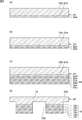
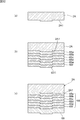
- FIG. 8C are front sectional views for explaining a process of providing an acoustic reflection layer and a support layer in the third embodiment of the present invention.
- FIG. 9A and FIG. 9B are front cross-sectional views for explaining a process of providing an acoustic reflection layer and a support layer in the third embodiment of the present invention.
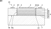
- FIG. 10 is a front sectional view of an acoustic wave device according to the fourth embodiment of the present invention.
- FIG. 11 is front sectional drawing which shows the state before dicing of the elastic wave apparatus which concerns on the 5th Embodiment of this invention.
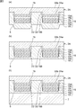
- 12 (a) to 12 (c) are front sectional views for explaining a manufacturing process of the acoustic wave device according to the fifth embodiment of the present invention.
- FIG. 13A to FIG. 13C are front sectional views for explaining a manufacturing process of the acoustic wave device according to the fifth embodiment of the present invention.
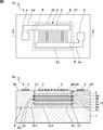
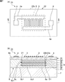
- FIG. 1A is a plan view of an acoustic wave device according to a first embodiment of the present invention.
- FIG. 1B is a cross-sectional view of the acoustic wave device taken along the line AA in FIG.
- the material of the support layer 6 is not particularly limited, and may be made of an appropriate material other than silicon oxide.
- the support layer 6 and the low acoustic impedance layers 5a, 5c, 5e may be made of different materials.
- the feature of the acoustic wave device of the present invention is that the acoustic reflection layer is surrounded by the support layer in a plan view from the second main surface 2b side of the piezoelectric layer 2.
- the acoustic reflection layer is surrounded by the support layer in a plan view from the second main surface 2b side of the piezoelectric layer 2.
- the acoustic reflection layer 5 is provided so as to overlap at least the IDT electrode 3 in a plan view from the second main surface 2b side of the piezoelectric layer 2.
- the energy of the elastic wave propagating to the first main surface 2a of the piezoelectric layer 2 is particularly large at a position overlapping the IDT electrode 3. Therefore, the acoustic reflection layer 5 can effectively confine the energy of the elastic wave.
- the interface between all the low acoustic impedance layers 5a, 5c, 5e and the high acoustic impedance layers 5b, 5d, 5f of the acoustic reflection layer 5 is located between the piezoelectric layer 2 and the bottom 6c2. Therefore, even if the acoustic reflection layer 5 is in contact with the bottom portion 6c2, the acoustic reflection layer 5 can sufficiently exhibit the function of reflecting the elastic wave propagated from the piezoelectric layer 2. Therefore, the energy of the elastic wave can be effectively confined and the strength of the elastic wave device can be increased.
- the low acoustic impedance layer 5cB has a low acoustic impedance layer 5c and a support layer forming portion 6Ac.
- the low acoustic impedance layer 5c becomes the low acoustic impedance layer 5c of the acoustic reflection layer 5 shown in FIG.
- the support layer forming portion 6Ac is a part of the support layer 6.
Landscapes
- Physics & Mathematics (AREA)
- Acoustics & Sound (AREA)
- Engineering & Computer Science (AREA)
- Manufacturing & Machinery (AREA)
- Surface Acoustic Wave Elements And Circuit Networks Thereof (AREA)
Abstract
Description
2…圧電体層
2a,2b…第1,第2の主面
2A…マザー基板
2A1…突出部
2Aa,2Ab…第1,第2の主面
3…IDT電極
4…電極ランド
4a…配線
5…音響反射層
5A…マザーの音響反射層
5a,5c,5e,5aA,5aB,5cA,5cB,5eA…低音響インピーダンス層
5b,5d,5f,5bA,5dA,5fA…高音響インピーダンス層
5b1…エッジ部
6…支持層
6A,6Aa,6Ac…支持層形成部
6a,6b…第1,第2の面
6c…開口部
6c1…側面部
6c2…底部
7…補強基板
11…弾性波装置
15…音響反射層
15B…外周部
15a,15c,15e…低音響インピーダンス層
15b,15d,15f…高音響インピーダンス層
21…弾性波装置
22…圧電体層
22a,22b…第1,第2の主面
31…弾性波装置
32…圧電体層
32a,32b…第1,第2の主面
33a…第1の励振電極
33b…第2の励振電極
41…弾性波装置
46…支持層
46c…開口部
51…弾性波装置
61…弾性波装置
65…音響反射層
65a,65c,65e…低音響インピーダンス層
65b,65d,65f…高音響インピーダンス層
66…平坦化膜
Claims (14)
- 第1の主面と、該第1の主面に対向している第2の主面と、を有する圧電体層と、
前記圧電体層の前記第1の主面上に積層されている音響反射層と、
前記圧電体層に設けられている励振電極と、
支持層と、
を備え、
前記音響反射層は、前記圧電体層の前記第2の主面側からの平面視において、少なくとも前記励振電極と重なるように位置しており、
前記支持層は、
少なくとも、前記圧電体層の第2の主面側からの平面視において、前記音響反射層を囲むように設けられている、弾性波装置。 - 前記支持層が、前記圧電体層の前記第2の主面側からの平面視において、前記圧電体層を囲むように設けられている、請求項1に記載の弾性波装置。
- 前記音響反射層が複数の音響インピーダンス層を有し、
前記複数の音響インピーダンス層が、少なくとも1層の低音響インピーダンス層と、前記低音響インピーダンス層よりも音響インピーダンスが高い、少なくとも1層の高音響インピーダンス層と、を有する、請求項1または2に記載の弾性波装置。 - 前記複数の音響インピーダンス層の内少なくとも1層の外側に空隙が配置されている、請求項1~3のいずれか1項に記載の弾性波装置。
- 前記低音響インピーダンス層及び前記高音響インピーダンス層の内のいずれか一方が前記支持層の一部である、請求項3または4に記載の弾性波装置。
- 前記低音響インピーダンス層及び前記高音響インピーダンス層の内、外側に前記空隙が配置されている層が金属層である、請求項5に記載の弾性波装置。
- 前記空隙が、前記複数の音響インピーダンス層の内、積層方向に連続した少なくとも2層の外側に位置している、請求項4~6のいずれか1項に記載の弾性波装置。
- 前記支持層は、底部を有する開口部を備えており、
前記音響反射層は、前記底部と接触している、請求項1~7のいずれか1項に記載の弾性波装置。 - 前記励振電極がIDT電極であり、かつ前記IDT電極が前記圧電体層の前記第2の主面に設けられている、請求項1~8のいずれか1項に記載の弾性波装置。
- 前記励振電極が第1,第2の励振電極を有し、前記第1の励振電極が前記圧電体層の前記第1の主面に設けられており、前記第2の励振電極が前記第2の主面に設けられている、請求項1~8のいずれか1項に記載の弾性波装置。
- 前記支持層の前記圧電体層側とは反対側に設けられている補強基板をさらに備える、請求項1~10のいずれか1項に記載の弾性波装置。
- 前記音響反射層、または前記複数の音響インピーダンス層の内少なくとも1つの層が、酸化ケイ素である、請求項1~11のいずれか1項に記載の弾性波装置。
- 第1の主面と、該第1の主面に対向している第2の主面と、を有し、かつ圧電体層からなるマザー基板の前記第1の主面上に、音響反射層を積層する工程と、
前記音響反射層をパターニングし、複数の音響反射層に分割する工程と、
前記マザー基板の前記第1の主面上及び前記複数の音響反射層上に支持層を設ける工程と、
前記マザー基板に複数の励振電極を設ける工程と、
前記支持層をダイシングすることにより、個々の弾性波装置に分割する工程と、
を備え、
前記支持層を設ける工程は、
前記支持層を、前記圧電体層の前記第2の主面側からの平面視において、各前記音響反射層を囲むように設ける工程であり、
前記音響反射層を積層する工程は、前記音響反射層を、前記圧電体層の前記第2の主面側からの平面視において、少なくとも各前記励振電極と重なる位置に設ける工程である、弾性波装置の製造方法。 - 前記マザー基板上に前記音響反射層を積層する工程は、複数の音響インピーダンス層を積層する工程であり、
前記複数の音響インピーダンス層は、少なくとも1層の低音響インピーダンス層と、前記低音響インピーダンス層よりも音響インピーダンスが高い、少なくとも1層の高音響インピーダンス層と、を有し、
前記音響反射層を積層する工程及び前記音響反射層をパターニングする工程は、前記低音響インピーダンス層及び前記高音響インピーダンス層の内のいずれか一方をパターニングした後に、該パターニングした音響インピーダンス層を覆うように別の音響インピーダンス層を積層し、前記パターニングした音響インピーダンス層の外側に空隙を配置する工程である、請求項13に記載の弾性波装置の製造方法。
Priority Applications (4)
| Application Number | Priority Date | Filing Date | Title |
|---|---|---|---|
| CN201680014166.6A CN107408936B (zh) | 2015-03-16 | 2016-03-09 | 弹性波装置及其制造方法 |
| KR1020177020923A KR101923573B1 (ko) | 2015-03-16 | 2016-03-09 | 탄성파 장치 및 그 제조 방법 |
| US15/679,324 US11152914B2 (en) | 2015-03-16 | 2017-08-17 | Elastic wave device and method for manufacturing the same |
| US17/503,415 US12261585B2 (en) | 2015-03-16 | 2021-10-18 | Elastic wave device and method for manufacturing the same |
Applications Claiming Priority (2)
| Application Number | Priority Date | Filing Date | Title |
|---|---|---|---|
| JP2015051816 | 2015-03-16 | ||
| JP2015-051816 | 2015-03-16 |
Related Child Applications (1)
| Application Number | Title | Priority Date | Filing Date |
|---|---|---|---|
| US15/679,324 Continuation US11152914B2 (en) | 2015-03-16 | 2017-08-17 | Elastic wave device and method for manufacturing the same |
Publications (1)
| Publication Number | Publication Date |
|---|---|
| WO2016147986A1 true WO2016147986A1 (ja) | 2016-09-22 |
Family
ID=56918849
Family Applications (1)
| Application Number | Title | Priority Date | Filing Date |
|---|---|---|---|
| PCT/JP2016/057411 Ceased WO2016147986A1 (ja) | 2015-03-16 | 2016-03-09 | 弾性波装置及びその製造方法 |
Country Status (4)
| Country | Link |
|---|---|
| US (1) | US11152914B2 (ja) |
| KR (1) | KR101923573B1 (ja) |
| CN (1) | CN107408936B (ja) |
| WO (1) | WO2016147986A1 (ja) |
Cited By (7)
| Publication number | Priority date | Publication date | Assignee | Title |
|---|---|---|---|---|
| WO2018235731A1 (ja) * | 2017-06-23 | 2018-12-27 | 株式会社村田製作所 | 弾性波装置、高周波フロントエンド回路および通信装置 |
| WO2019065667A1 (ja) * | 2017-09-27 | 2019-04-04 | 株式会社村田製作所 | 弾性波フィルタ装置 |
| WO2019065669A1 (ja) * | 2017-09-27 | 2019-04-04 | 株式会社村田製作所 | 弾性波装置及び弾性波装置の製造方法 |
| WO2019065666A1 (ja) * | 2017-09-27 | 2019-04-04 | 株式会社村田製作所 | 弾性波装置 |
| WO2020116528A1 (ja) * | 2018-12-06 | 2020-06-11 | 株式会社村田製作所 | 弾性波装置 |
| CN116760386A (zh) * | 2023-05-30 | 2023-09-15 | 无锡市好达电子股份有限公司 | 弹性波器件 |
| JP7654482B2 (ja) | 2021-06-24 | 2025-04-01 | 太陽誘電株式会社 | 弾性波デバイス、フィルタ、マルチプレクサ、およびウエハ |
Families Citing this family (17)
| Publication number | Priority date | Publication date | Assignee | Title |
|---|---|---|---|---|
| US9537465B1 (en) * | 2014-06-06 | 2017-01-03 | Akoustis, Inc. | Acoustic resonator device with single crystal piezo material and capacitor on a bulk substrate |
| US12261585B2 (en) * | 2015-03-16 | 2025-03-25 | Murata Manufacturing Co., Ltd. | Elastic wave device and method for manufacturing the same |
| US11218133B2 (en) * | 2016-09-30 | 2022-01-04 | Intel Corporation | Film bulk acoustic resonator (FBAR) devices for high frequency RF filters |
| WO2019124126A1 (ja) * | 2017-12-22 | 2019-06-27 | 株式会社村田製作所 | 弾性波装置、高周波フロントエンド回路及び通信装置並びに弾性波装置の製造方法 |
| KR102251000B1 (ko) * | 2018-12-28 | 2021-05-12 | (주)와이팜 | 에너지 누화를 최소화하는 다층 구조의 saw 공진기 및 제조 방법 |
| JP2020113954A (ja) * | 2019-01-16 | 2020-07-27 | 株式会社村田製作所 | 弾性波装置 |
| JP7259872B2 (ja) * | 2019-01-31 | 2023-04-18 | 株式会社村田製作所 | 弾性波装置 |
| DE102019120178B4 (de) | 2019-07-25 | 2021-09-30 | RF360 Europe GmbH | Elektroakustische Filterkomponente und Herstellungsverfahren |
| US11463065B2 (en) * | 2019-12-03 | 2022-10-04 | Skyworks Solutions, Inc. | Laterally excited bulk wave device with acoustic mirror |
| US11552614B2 (en) | 2019-12-03 | 2023-01-10 | Skyworks Solutions, Inc. | Laterally excited bulk wave device with acoustic mirrors |
| CN113098431B (zh) | 2020-01-08 | 2023-09-08 | 中芯集成电路(宁波)有限公司 | 用于制作声波谐振器复合基板及表声波谐振器及制造方法 |
| WO2021200677A1 (ja) * | 2020-03-31 | 2021-10-07 | 株式会社村田製作所 | 弾性波装置 |
| US20220321088A1 (en) | 2021-03-31 | 2022-10-06 | Skyworks Solutions, Inc. | Acoustic wave device with double side acoustic mirror |
| CN113381721B (zh) * | 2021-05-06 | 2023-08-08 | 偲百创(深圳)科技有限公司 | 压电换能器制作方法及压电换能器 |
| US11823483B2 (en) * | 2021-09-17 | 2023-11-21 | Qualcomm Incorporated | Apparatus with ultrasonic fingerprint sensor and one or more resonators, and related systems and methods |
| US12615033B2 (en) | 2021-10-04 | 2026-04-28 | Skyworks Solutions, Inc. | Stacked single mirror acoustic wave device and double mirror acoustic wave device |
| US12531541B2 (en) | 2021-10-05 | 2026-01-20 | Skyworks Solutions, Inc. | Stacked structure with multiple acoustic wave devices |
Citations (9)
| Publication number | Priority date | Publication date | Assignee | Title |
|---|---|---|---|---|
| US6548942B1 (en) * | 1997-02-28 | 2003-04-15 | Texas Instruments Incorporated | Encapsulated packaging for thin-film resonators and thin-film resonator-based filters having a piezoelectric resonator between two acoustic reflectors |
| JP2005159606A (ja) * | 2003-11-25 | 2005-06-16 | Tdk Corp | 圧電薄膜共振器およびその製造方法 |
| WO2007026637A1 (ja) * | 2005-08-30 | 2007-03-08 | Matsushita Electric Industrial Co., Ltd. | 圧電共振器及び圧電共振器の製造方法 |
| WO2012086639A1 (ja) * | 2010-12-24 | 2012-06-28 | 株式会社村田製作所 | 弾性波装置及びその製造方法 |
| WO2012137574A1 (ja) * | 2011-04-01 | 2012-10-11 | ルネサスエレクトロニクス株式会社 | 半導体装置およびその製造方法ならびに携帯電話機 |
| JP2013214954A (ja) * | 2012-03-07 | 2013-10-17 | Taiyo Yuden Co Ltd | 共振子、周波数フィルタ、デュプレクサ、電子機器及び共振子の製造方法 |
| JP2013223025A (ja) * | 2012-04-13 | 2013-10-28 | Taiyo Yuden Co Ltd | フィルタ装置、フィルタ装置の製造方法及びデュプレクサ |
| JP2014176095A (ja) * | 2013-03-12 | 2014-09-22 | Triquint Semiconductor Inc | 強固に固定されたバルク弾性波共振器における境界リングモード抑制 |
| JP2015228620A (ja) * | 2014-06-02 | 2015-12-17 | 日本電波工業株式会社 | 圧電素子、圧電デバイス、圧電素子の製造方法、及び圧電デバイスの製造方法 |
Family Cites Families (15)
| Publication number | Priority date | Publication date | Assignee | Title |
|---|---|---|---|---|
| US6496085B2 (en) * | 2001-01-02 | 2002-12-17 | Nokia Mobile Phones Ltd | Solidly mounted multi-resonator bulk acoustic wave filter with a patterned acoustic mirror |
| US6509813B2 (en) * | 2001-01-16 | 2003-01-21 | Nokia Mobile Phones Ltd. | Bulk acoustic wave resonator with a conductive mirror |
| US7098574B2 (en) * | 2002-11-08 | 2006-08-29 | Toyo Communication Equipment Co., Ltd. | Piezoelectric resonator and method for manufacturing the same |
| TWI256194B (en) * | 2004-12-30 | 2006-06-01 | Delta Electronics Inc | Filter assembly with unbalanced to balanced conversion |
| FR2882205B1 (fr) | 2005-02-16 | 2007-06-22 | Centre Nat Rech Scient | Dispositif a ondes acoustiques haute frequence |
| JP2007208845A (ja) * | 2006-02-03 | 2007-08-16 | Matsushita Electric Ind Co Ltd | 圧電共振器 |
| JPWO2009013938A1 (ja) * | 2007-07-20 | 2010-09-30 | 株式会社村田製作所 | 圧電共振子及び圧電フィルタ装置 |
| WO2009023100A2 (en) * | 2007-08-14 | 2009-02-19 | Skyworks Solutions, Inc. | Method for forming a multi-layer electrode underlying a piezoelectric layer and related structure |
| US8514033B2 (en) * | 2007-10-18 | 2013-08-20 | Avago Technologies General Ip (Singapore) Pte. Ltd. | BAW structure with reduced topographic steps and related method |
| US9735338B2 (en) * | 2009-01-26 | 2017-08-15 | Cymatics Laboratories Corp. | Protected resonator |
| CN103283147B (zh) * | 2010-12-24 | 2016-09-21 | 株式会社村田制作所 | 弹性波装置及其制造方法 |
| US20140117815A1 (en) * | 2012-10-26 | 2014-05-01 | Avago Technologies General Ip (Singapore) Pte. Ltd | Temperature compensated resonator device having low trim sensitivy and method of fabricating the same |
| US9225313B2 (en) * | 2012-10-27 | 2015-12-29 | Avago Technologies General Ip (Singapore) Pte. Ltd. | Bulk acoustic wave resonator having doped piezoelectric layer with improved piezoelectric characteristics |
| US20160268554A1 (en) * | 2015-03-11 | 2016-09-15 | National Taiwan University | Electroluminescent devices with improved optical out-coupling efficiencies |
| CN110392978B (zh) * | 2017-02-21 | 2023-04-04 | 株式会社村田制作所 | 弹性波装置、高频前端电路以及通信装置 |
-
2016
- 2016-03-09 WO PCT/JP2016/057411 patent/WO2016147986A1/ja not_active Ceased
- 2016-03-09 KR KR1020177020923A patent/KR101923573B1/ko active Active
- 2016-03-09 CN CN201680014166.6A patent/CN107408936B/zh active Active
-
2017
- 2017-08-17 US US15/679,324 patent/US11152914B2/en active Active
Patent Citations (9)
| Publication number | Priority date | Publication date | Assignee | Title |
|---|---|---|---|---|
| US6548942B1 (en) * | 1997-02-28 | 2003-04-15 | Texas Instruments Incorporated | Encapsulated packaging for thin-film resonators and thin-film resonator-based filters having a piezoelectric resonator between two acoustic reflectors |
| JP2005159606A (ja) * | 2003-11-25 | 2005-06-16 | Tdk Corp | 圧電薄膜共振器およびその製造方法 |
| WO2007026637A1 (ja) * | 2005-08-30 | 2007-03-08 | Matsushita Electric Industrial Co., Ltd. | 圧電共振器及び圧電共振器の製造方法 |
| WO2012086639A1 (ja) * | 2010-12-24 | 2012-06-28 | 株式会社村田製作所 | 弾性波装置及びその製造方法 |
| WO2012137574A1 (ja) * | 2011-04-01 | 2012-10-11 | ルネサスエレクトロニクス株式会社 | 半導体装置およびその製造方法ならびに携帯電話機 |
| JP2013214954A (ja) * | 2012-03-07 | 2013-10-17 | Taiyo Yuden Co Ltd | 共振子、周波数フィルタ、デュプレクサ、電子機器及び共振子の製造方法 |
| JP2013223025A (ja) * | 2012-04-13 | 2013-10-28 | Taiyo Yuden Co Ltd | フィルタ装置、フィルタ装置の製造方法及びデュプレクサ |
| JP2014176095A (ja) * | 2013-03-12 | 2014-09-22 | Triquint Semiconductor Inc | 強固に固定されたバルク弾性波共振器における境界リングモード抑制 |
| JP2015228620A (ja) * | 2014-06-02 | 2015-12-17 | 日本電波工業株式会社 | 圧電素子、圧電デバイス、圧電素子の製造方法、及び圧電デバイスの製造方法 |
Cited By (20)
| Publication number | Priority date | Publication date | Assignee | Title |
|---|---|---|---|---|
| CN110809857A (zh) * | 2017-06-23 | 2020-02-18 | 株式会社村田制作所 | 弹性波装置、高频前端电路以及通信装置 |
| US11309862B2 (en) | 2017-06-23 | 2022-04-19 | Murata Manufacturing Co., Ltd | Acoustic wave device, high frequency front end circuit, and communication apparatus |
| WO2018235731A1 (ja) * | 2017-06-23 | 2018-12-27 | 株式会社村田製作所 | 弾性波装置、高周波フロントエンド回路および通信装置 |
| JPWO2018235731A1 (ja) * | 2017-06-23 | 2020-04-02 | 株式会社村田製作所 | 弾性波装置、高周波フロントエンド回路および通信装置 |
| US12143097B2 (en) | 2017-09-27 | 2024-11-12 | Murata Manufacturing Co., Ltd. | Acoustic wave filter device |
| WO2019065666A1 (ja) * | 2017-09-27 | 2019-04-04 | 株式会社村田製作所 | 弾性波装置 |
| US11509281B2 (en) | 2017-09-27 | 2022-11-22 | Murata Manufacturing Co., Ltd. | Acoustic wave device |
| JPWO2019065666A1 (ja) * | 2017-09-27 | 2020-07-02 | 株式会社村田製作所 | 弾性波装置 |
| JPWO2019065667A1 (ja) * | 2017-09-27 | 2020-07-09 | 株式会社村田製作所 | 弾性波フィルタ装置 |
| JPWO2019065669A1 (ja) * | 2017-09-27 | 2020-07-09 | 株式会社村田製作所 | 弾性波装置及び弾性波装置の製造方法 |
| WO2019065669A1 (ja) * | 2017-09-27 | 2019-04-04 | 株式会社村田製作所 | 弾性波装置及び弾性波装置の製造方法 |
| WO2019065667A1 (ja) * | 2017-09-27 | 2019-04-04 | 株式会社村田製作所 | 弾性波フィルタ装置 |
| US11309866B2 (en) | 2017-09-27 | 2022-04-19 | Murata Manufacturing Co., Ltd | Acoustic wave device and method for manufacturing acoustic wave device |
| JPWO2020116528A1 (ja) * | 2018-12-06 | 2021-10-14 | 株式会社村田製作所 | 弾性波装置 |
| JP7205551B2 (ja) | 2018-12-06 | 2023-01-17 | 株式会社村田製作所 | 弾性波装置 |
| US11799443B2 (en) | 2018-12-06 | 2023-10-24 | Murata Manufacturing Co., Ltd. | Acoustic wave device |
| WO2020116528A1 (ja) * | 2018-12-06 | 2020-06-11 | 株式会社村田製作所 | 弾性波装置 |
| JP7654482B2 (ja) | 2021-06-24 | 2025-04-01 | 太陽誘電株式会社 | 弾性波デバイス、フィルタ、マルチプレクサ、およびウエハ |
| CN116760386A (zh) * | 2023-05-30 | 2023-09-15 | 无锡市好达电子股份有限公司 | 弹性波器件 |
| CN116760386B (zh) * | 2023-05-30 | 2024-02-13 | 无锡市好达电子股份有限公司 | 弹性波器件 |
Also Published As
| Publication number | Publication date |
|---|---|
| CN107408936B (zh) | 2020-12-11 |
| KR20170097781A (ko) | 2017-08-28 |
| US20170366163A1 (en) | 2017-12-21 |
| US11152914B2 (en) | 2021-10-19 |
| CN107408936A (zh) | 2017-11-28 |
| KR101923573B1 (ko) | 2018-11-29 |
Similar Documents
| Publication | Publication Date | Title |
|---|---|---|
| WO2016147986A1 (ja) | 弾性波装置及びその製造方法 | |
| JP6642499B2 (ja) | 弾性波装置 | |
| CN107251427B (zh) | 弹性波装置及其制造方法 | |
| JP7081041B2 (ja) | 薄膜バルク音響波共振器とその製造方法、フィルタ、および無線周波数通信システム | |
| JP4661958B2 (ja) | 圧電共振子及び圧電フィルタ | |
| JP5648695B2 (ja) | 弾性波装置及びその製造方法 | |
| JP6631925B2 (ja) | 圧電薄膜素子の製造方法 | |
| WO2017212774A1 (ja) | 弾性波装置及びその製造方法 | |
| WO2018154950A1 (ja) | 弾性波装置、高周波フロントエンド回路及び通信装置 | |
| JP6464735B2 (ja) | 弾性波装置及びその製造方法 | |
| CN107615657A (zh) | 弹性波装置 | |
| CN107615658A (zh) | 弹性波装置 | |
| CN114955976B (zh) | 一种mems器件及其制作方法 | |
| WO2017043151A1 (ja) | 弾性波装置 | |
| WO2021053884A1 (ja) | 圧電素子およびその製造方法 | |
| US10924083B2 (en) | Piezoelectric device and method for manufacturing piezoelectric device | |
| WO2022158249A1 (ja) | 弾性波装置、フィルタ装置及び弾性波装置の製造方法 | |
| JP2007081613A (ja) | 弾性表面波デバイス及びその製造方法 | |
| US12261585B2 (en) | Elastic wave device and method for manufacturing the same | |
| CN114342098A (zh) | 压电元件 | |
| JP4655796B2 (ja) | 弾性境界波装置の製造方法及び弾性境界波装置 | |
| JP5288116B2 (ja) | 圧電振動子およびその製造方法 | |
| WO2025047333A1 (ja) | 弾性波装置 | |
| WO2024247530A1 (ja) | 弾性波装置 | |
| JP2004064214A (ja) | 積層型圧電部品の製造方法 |
Legal Events
| Date | Code | Title | Description |
|---|---|---|---|
| 121 | Ep: the epo has been informed by wipo that ep was designated in this application |
Ref document number: 16764816 Country of ref document: EP Kind code of ref document: A1 |
|
| ENP | Entry into the national phase |
Ref document number: 20177020923 Country of ref document: KR Kind code of ref document: A |
|
| NENP | Non-entry into the national phase |
Ref country code: DE |
|
| 122 | Ep: pct application non-entry in european phase |
Ref document number: 16764816 Country of ref document: EP Kind code of ref document: A1 |
|
| NENP | Non-entry into the national phase |
Ref country code: JP |