WO2016143845A1 - 電子部品封止用キャップ - Google Patents
電子部品封止用キャップ Download PDFInfo
- Publication number
- WO2016143845A1 WO2016143845A1 PCT/JP2016/057530 JP2016057530W WO2016143845A1 WO 2016143845 A1 WO2016143845 A1 WO 2016143845A1 JP 2016057530 W JP2016057530 W JP 2016057530W WO 2016143845 A1 WO2016143845 A1 WO 2016143845A1
- Authority
- WO
- WIPO (PCT)
- Prior art keywords
- cap
- brazing material
- sealing
- electronic component
- shape
- Prior art date
- Legal status (The legal status is an assumption and is not a legal conclusion. Google has not performed a legal analysis and makes no representation as to the accuracy of the status listed.)
- Ceased
Links
Images




Classifications
-
- H—ELECTRICITY
- H10—SEMICONDUCTOR DEVICES; ELECTRIC SOLID-STATE DEVICES NOT OTHERWISE PROVIDED FOR
- H10W—GENERIC PACKAGES, INTERCONNECTIONS, CONNECTORS OR OTHER CONSTRUCTIONAL DETAILS OF DEVICES COVERED BY CLASS H10
- H10W76/00—Containers; Fillings or auxiliary members therefor; Seals
- H10W76/10—Containers or parts thereof
- H10W76/12—Containers or parts thereof characterised by their shape
- H10W76/13—Containers comprising a conductive base serving as an interconnection
- H10W76/138—Containers comprising a conductive base serving as an interconnection having another interconnection being formed by a cover plate parallel to the conductive base, e.g. sandwich type
-
- H—ELECTRICITY
- H10—SEMICONDUCTOR DEVICES; ELECTRIC SOLID-STATE DEVICES NOT OTHERWISE PROVIDED FOR
- H10W—GENERIC PACKAGES, INTERCONNECTIONS, CONNECTORS OR OTHER CONSTRUCTIONAL DETAILS OF DEVICES COVERED BY CLASS H10
- H10W74/00—Encapsulations, e.g. protective coatings
-
- H—ELECTRICITY
- H10—SEMICONDUCTOR DEVICES; ELECTRIC SOLID-STATE DEVICES NOT OTHERWISE PROVIDED FOR
- H10W—GENERIC PACKAGES, INTERCONNECTIONS, CONNECTORS OR OTHER CONSTRUCTIONAL DETAILS OF DEVICES COVERED BY CLASS H10
- H10W74/00—Encapsulations, e.g. protective coatings
- H10W74/40—Encapsulations, e.g. protective coatings characterised by their materials
- H10W74/481—Encapsulations, e.g. protective coatings characterised by their materials comprising semiconductor materials
-
- H—ELECTRICITY
- H10—SEMICONDUCTOR DEVICES; ELECTRIC SOLID-STATE DEVICES NOT OTHERWISE PROVIDED FOR
- H10W—GENERIC PACKAGES, INTERCONNECTIONS, CONNECTORS OR OTHER CONSTRUCTIONAL DETAILS OF DEVICES COVERED BY CLASS H10
- H10W76/00—Containers; Fillings or auxiliary members therefor; Seals
- H10W76/10—Containers or parts thereof
-
- H—ELECTRICITY
- H10—SEMICONDUCTOR DEVICES; ELECTRIC SOLID-STATE DEVICES NOT OTHERWISE PROVIDED FOR
- H10W—GENERIC PACKAGES, INTERCONNECTIONS, CONNECTORS OR OTHER CONSTRUCTIONAL DETAILS OF DEVICES COVERED BY CLASS H10
- H10W76/00—Containers; Fillings or auxiliary members therefor; Seals
- H10W76/60—Seals
-
- H—ELECTRICITY
- H10—SEMICONDUCTOR DEVICES; ELECTRIC SOLID-STATE DEVICES NOT OTHERWISE PROVIDED FOR
- H10W—GENERIC PACKAGES, INTERCONNECTIONS, CONNECTORS OR OTHER CONSTRUCTIONAL DETAILS OF DEVICES COVERED BY CLASS H10
- H10W72/00—Interconnections or connectors in packages
- H10W72/50—Bond wires
- H10W72/551—Materials of bond wires
- H10W72/552—Materials of bond wires comprising metals or metalloids, e.g. silver
- H10W72/5522—Materials of bond wires comprising metals or metalloids, e.g. silver comprising gold [Au]
Definitions
- the present invention relates to a cap (cover) used for manufacturing packages of various electronic components.
- the present invention provides a sealing cap that can suppress excessive wetting and spreading of the brazing material during sealing, and can reduce the amount of gold plating when the brazing material is fused and fixed.
- a sealed structure is generally formed by covering a base on which an element is placed and fixed with a cap serving as a lid.
- the shape of the base and cap of the sealed package there are many cases where a flat cap is combined with a container-like base having a cavity. Recently, conversely, a structure has been reported in which a cavity is formed on the cap, the element is fixed to a flat base, and the cap is joined.
- the structure in which the cavity is formed in the cap is a form which has been attracting attention in recent years because it can contribute to the cost reduction of the device by making the process of fixing the element to the base efficient.
- FIG. 1 illustrates a manufacturing process of a package to which a cap and a base are applied.
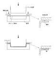
- FIG. 2 illustrates the process of fusing and fixing the brazing material to the cap before sealing the package.
- Both flat plate caps and caps with cavities have a brazing material fusion surface considering the package specifications.
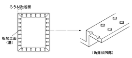
- a frame-shaped brazing material fusion surface is set along the four sides (FIG. 2A).
- the cap with cavity is set with a frame-like brazing material fusion surface on the end face (FIG. 2B).
- the end surface of the cap body forming the cavity is bent to form a flange-like flange portion, and this flange surface is used as a brazing material fusion surface.
- a frame-like brazing material (Au-based brazing material) is fused and fixed to these brazing material fusion surfaces, but before that, it is common to apply Au plating to the cap surface.
- This is in consideration of the material of the cap (Kovar (Fe—Ni—Co alloy), 42 alloy (Fe—Ni alloy) or the like is used). That is, since the melted Au-based brazing material has poor wettability and the frame shape may collapse when melted, Au plating is applied to ensure the wettability of the cap surface. In order to prevent the oxidation of Kovar, Ni plating may be applied before Au plating. And after performing the plating process in this way, the brazing material is fused.
- a cap for sealing in consideration of the wetting and spreading of the brazing material at the time of sealing, for example, there is a cap (lid) described in Patent Document 1.
- This cap is related to a flat plate cap, and is manufactured by storing Ni-plated and Au-plated caps with a frame-shaped brazing material fused together with a polishing medium in a container, and shaking the container for polishing. Is done. By this polishing, most of the Au plating on the inner side of the cap is peeled off, and the remaining trace amount of Au and Ni plating are alloyed. Since the Au-based brazing material does not have good wettability with respect to the Ni alloy, the flow spread of the brazing material can be controlled.
- the peeling of the Au plating on the cap surface as described above has a temporary effect on the problem of wetting and spreading of the brazing material.
- this approach may be useful for plate caps, but is not effective for caps with deep cavities. This is because it is predicted that sufficient polishing is not performed on a step such as a side portion of the cavity.
- the Au plating has been pointed out from another viewpoint of resource saving.
- Au is a noble metal and an expensive metal. According to the recent demand for cost reduction, the amount of Au plating should be as small as possible. However, in order to exhibit wettability to the molten brazing material, a certain amount or more of Au is required on the cap surface. Therefore, the amount of plating cannot be reduced easily.
- the present invention has been made under the background as described above.
- the cap for package sealing can exhibit suitable wettability when fusing an Au-based brazing material, while sealing. Provided is one capable of suppressing the wetting and spreading of the brazing material remelted during the stopping operation. This effect is exhibited regardless of the form of the cap. At the same time, a cap capable of reducing the amount of plating when Au plating is performed is provided.
- the present invention which solves the above-mentioned problems is a cap for an electronic component for manufacturing a package having a sealing region by bonding to a base, a brazing material fusion surface for fusing a brazing material, and the sealing A sealing surface corresponding to a region, the brazing material fusion surface having a non-planar work surface formed by plastic working, and a surface area (Sc) per unit area of the brazing material fusion surface.
- the surface area per unit area (Sf) of the sealing surface (Sc / Sf) is 1 ⁇ Sc / Sf ⁇ 1.6.
- the surface on which the brazing material is fused (the brazing material fusion surface) is changed from a flat surface to a three-dimensional one.
- the surface area of the region is made larger than the surface area of the sealing region by providing a three-dimensional work surface on the brazing material fusion surface.
- the increase in surface area leads to an increase in the mass of Au deposited when Au plating is performed. That is, a state is formed in which the Au mass of the brazing material fusion surface is larger than the Au mass of the sealing surface.
- the conventional sealing cap is plated with the same amount of Au on the entire surface. However, it is sufficient that the necessary amount of Au is originally plated on the necessary portion (the brazing material fusion surface).
- the brazing material wettability is preferentially satisfied with respect to other locations by providing a gradient in the surface area and increasing the amount of Au plating on the brazing material fusion surface.
- the Au plating process can be completed at a timing earlier than before, and the amount of Au used is reduced.
- the ratio (Sc / Sf) of the surface area per unit area (Sc) of the brazing material fusion surface to the surface area per unit area (Sf) of the sealing surface is 1 ⁇ Sc / Sf ⁇ 1.6.
- the unit area is based on the horizontal projection area for the brazing material fusion surface and the sealing region.
- the surface area ratio (Sc / Sf) of both parts is set to a value larger than 1.
- Sc / Sf is preferably 1.005 ⁇ Sc / Sf ⁇ 1.5, more preferably 1.01 ⁇ Sc / Sf ⁇ 1.45, and further preferably 1.04 ⁇ Sc / Sf ⁇ 1.4. .
- the processed surface of the sealing cap according to the present invention will be described with examples as shown in FIGS.
- the cross-sectional shape of the surface to be processed is a shape having a groove protruding from the flat surface.
- the groove may have a rounded tip as shown in FIG. 3 or an acute angle groove.
- a plurality of grooves may be formed.
- the brazing material fusion surface may be inclined. As shown in FIG. 4, there is one having a linear inclination from the end toward the center.
- the cross-sectional shape at this time is substantially V-shaped.
- the slope of the processed surface may be curved, and as shown in FIG. 5, it may be processed to have an arc shape projecting downward from both ends toward the center.
- a machined surface having a circular arc in cross section is particularly suitable in some cases.
- the surface of the package may be subjected to a metallization process (material: tungsten) and an Au plating / Ni plating process to form an arc shape on the surface.
- a metallization process material: tungsten
- Au plating / Ni plating process to form an arc shape on the surface.
- partial unevenness may be formed. That is, at least one of a convex portion protruding upward and a concave portion protruding downward may be formed on the surface to be processed.
- FIG. 6 shows an example thereof, in which a plurality of pyramidal convex portions are formed on the brazing material fusion surface.
- the brazing material acts as a hot water sump for the brazing material melted at the tip of the groove or the inclined portion, and the convex portion acts as an obstacle to the brazing material. Prevent unwanted wetting spread.
- the vertical height and depth of the above processed surface be 3 ⁇ m or more and 15 ⁇ m or less with reference to both ends of the brazing filler metal.
- the constituent material of the sealing cap according to the present invention can be the same as that of the conventional cap.
- a Kovar alloy Fe—Ni—Co alloy
- 42 alloy Fe—Ni alloy
- the cap according to the present invention is used in a state where an Au-based brazing material is fused to the brazing material fusion surface.
- the Au brazing material include an Au—Sn brazing material (for example, Au-18 to 25% Sn), an Au—Ge brazing material (Au-10 to 15 wt% Ge), an Au—Si brazing material (Au— 2-5 wt% Si), Au—Sb brazing material (Au-30-40 wt% Sb) can be applied.
- the thickness of the Au-based brazing material after fusion is generally 5 ⁇ m or more and 30 ⁇ m or less.
- the Au brazing material when the Au brazing material is fused, it is preferable to have a Ni plating layer for ensuring the adhesion of the brazing material. Furthermore, it is preferable to use Au plating for securing wettability at the time of welding the brazing material.
- the Au plating formed on the brazing material fusion surface is integrated with the brazing material when the Au-based brazing material is subsequently fused. Therefore, in the cross section after the brazing material is fused, the layer structure of cap / Ni plating layer / brazing material is seen, and a clear Au plating layer is not observed.
- the shape of the cap of the present invention may be a flat plate shape. At this time, it is a general form that a frame-like brazing material fusion surface is set along the four sides.
- the present invention can be applied to a cap with a cavity and exhibits a preferable effect.
- This cap has a box shape in which a cavity is formed.
- the brazing material fusion surface can be frame-shaped along its end surface.
- the cap with the cavity may be a monolith composed of a cap body forming the cavity and a flange-shaped flange formed at the end thereof. At this time, a frame-shaped brazing material fusion surface can be set along the end surface of the flange.
- the cap manufacturing method according to the present invention described above is characterized by the formation of a processed surface.
- the processed surface can be formed after the cap is formed into various shapes. Moreover, it can carry out in parallel with the formation process of a cap.
- the processed surface can be formed by performing press processing using a mold corresponding to the processed surface on the brazing material fusion surface.
- the cap when the cap is formed in parallel in the cap forming process, for example, for a flat cap, the cap can be manufactured by shearing a sheet-like material. By performing the mold pressing at the same time as the shearing process at this time, it is possible to simultaneously perform the molding of the cap and the formation of the processed surface.
- a cap with a cavity can be formed and manufactured by drawing or molding a flat plate.
- drawing or molding a flat plate material is fixed to a jig, and a box-like body having a cavity is formed by pressing a tool against the material while suppressing an end portion thereof.
- the holding part at this time becomes a flange. Therefore, by forming a mold corresponding to the processed surface in the holding jig, a desired processed surface can be formed on the flange surface.
- the sealing cap according to the present invention controls the wetting and spreading of the brazing material melted at the time of sealing the package by providing a predetermined processing surface to the brazing material fusion surface. Can do. Further, the present invention can plate a sufficient amount of Au at a necessary place while limiting the plating amount of Au plating for fusion of a brazing material (Au-based brazing material).
- bonding surface (processed surface) in the cap for sealing which concerns on this invention.
- a sealing cap with a cavity having a flange and having a flange surface that is grooved is manufactured.
- a hoop material (dimensions: 14 mm ⁇ 1000 m, thickness 40 mm) made of Kovar was prepared as a cap manufacturing material.
- the hoop material was drawn using a progressive die to form a cavity, and then separated into individual pieces to produce a sealing cap.
- the hoop material was fed into a mold, the four sides thereof were restrained by a box-shaped jig, and the central part was pressed by a processing jig.
- the cap which has a box-shaped cavity is manufactured by the above process.
- the portion restrained by the restraining jig becomes a flange, but the surface of the restraining jig is formed with a linear protrusion, which forms a work surface (see FIG. 3) having a groove on the flange surface. To do.
- the dimensions of the cap after the molding process are, for example, a cavity dimension of 1.4 mm ⁇ 1.0 mm, a depth of 0.2 mm, and a flange surface width of 0.1 mm.
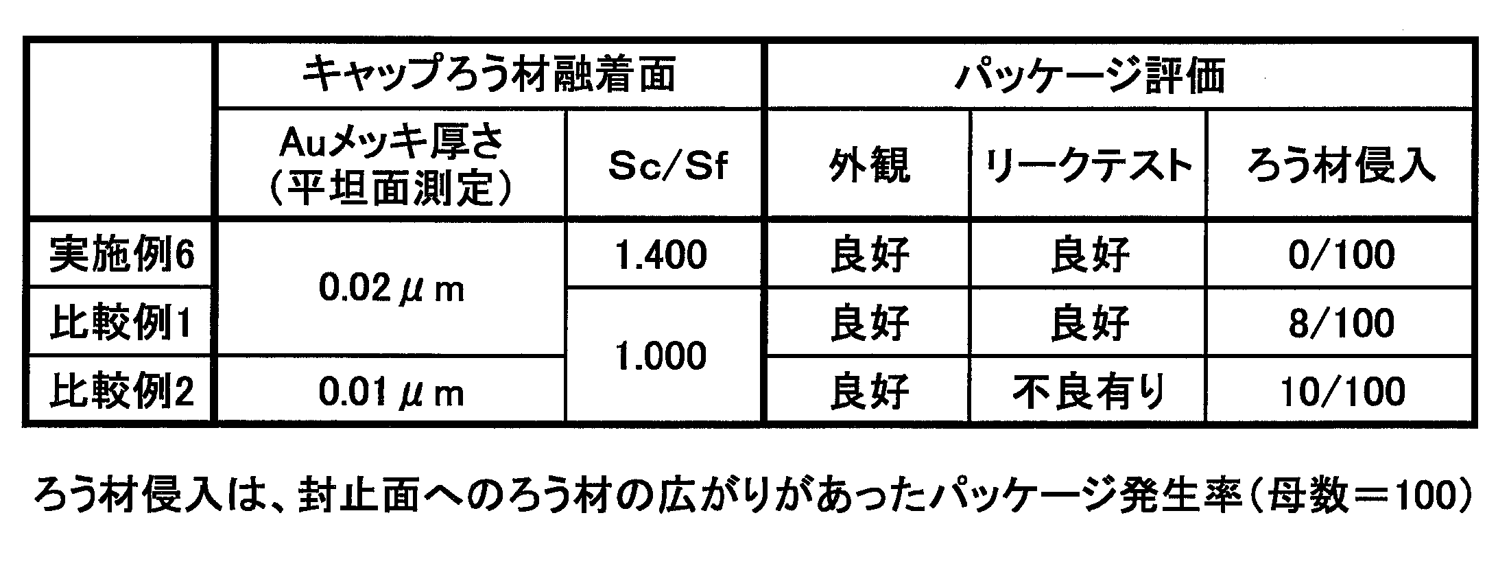
- the size of the linear convex portion of the restraining jig was changed, and five caps having different groove widths or depths on the flange surface and 100 caps without grooves were manufactured.
- Ni plating and Au plating were performed on the surface including the flange surface and the sealing surface.
- the plating process was performed by electrolytic barrel plating.
- the thickness of the flat part was measured to be 1 ⁇ m or more for Ni plating and 0.02 ⁇ m or less for Au plating.
- the brazing material was fused to the flange surface which is the brazing material fusion surface of the cap.
- a frame-shaped 80 wt% Au-20 wt% Sn brazing material (dimensions: outer dimensions 1.6 mm ⁇ 1.4 mm, inner dimensions 1.44 mm ⁇ 1.24 mm, thickness 13 ⁇ m) was fused.
- the fusing was performed by positioning the brazing material on the cap and placing it, and then inserting the brazing material into an electric furnace and heating it at 280 ° C. for 180 seconds to fuse the brazing material.
- the sealing caps manufactured (5 types ⁇ 100 solids) were subjected to a sealing test to confirm the wettability of the brazing material.
- the sealing test the manufactured cap is joined to a flat base (dimensions: 1.65 mm ⁇ 1.25 mm, thickness 0.15 mm, made of ceramic) (joining temperature 340 ° C.), and pseudo sealing is performed.
- a package was manufactured. Then, the appearance of the produced package was observed to confirm the presence or absence of the brazing material.
- a leak test was performed. In the leak test, the package was subjected to a helium leak detector, and the helium molecules after evacuation outside the package counted leaks to determine whether the hermetic seal was good or bad. Thereafter, the cap was removed from the package, and it was confirmed whether or not the brazing material had entered the sealing surface.
- a processed surface to be provided on the brazing material fusion surface of the cap is manufactured with a plurality of pyramidal concave portions formed (see FIG. 6).
- the basic manufacturing process of the cap is the same as that of the first embodiment, but the cap was processed using a surface jig having a plurality of pyramidal microprotrusions as the surface form of the restraining jig.
- the ratio (Sc / Sf) of the surface area per unit area (Sc) of the brazing material fusion surface to the surface area per unit area (Sf) of the sealing surface is approximately 1 .4.
- processing the brazing material fusion surface is also useful for stability when the brazing material is fused.
- the surface to be worked was not formed on the soldering surface of the brazing material, and the Au plating amount was further reduced.
- this cap was found to have leaked when the package was produced. there were.
- the cap in which the leak occurred several caps having a slightly distorted frame shape were observed instead of the rectangular frame shape in which the shape of the brazing material after fusion was prepared. It seems that hermetic sealing of the package was inadequate due to the use of such an irregularly shaped cap with brazing material. And in the cap which has such a brazing material, wetting spread does not become stable and brazing material intrusion to the sealing surface easily occurs.
- a sealing cap having a cross-section arc shape (see FIG. 5) was manufactured here.
- the basic manufacturing process of the cap is the same as that of the first embodiment, and the cap was processed using an arc-shaped restraining jig as shown in FIG.
- the ratio (Sc / Sf) of the surface area per unit area (Sc) of the brazing material fusion surface to the surface area per unit area (Sf) of the sealing surface is approximately 1 .01.
- FIG. 9 illustrates this sealing process, and a suitable joined state in which the work surface of the cap after the brazing filler metal is fused to the shape of the metallization can be obtained.
- 100 pseudo packages were manufactured, but no leakage or brazing material intrusion was observed even at a relatively thin (0.01 ⁇ m) brazing material thickness.
- the present invention high-quality products can be manufactured more stably than in the past for manufacturing sealed packages.
- the present invention is useful for manufacturing various semiconductor element devices such as SAW filters, FBAR filters, crystal resonators, and the like, and is also effective in reducing their costs.
Landscapes
- Piezo-Electric Or Mechanical Vibrators, Or Delay Or Filter Circuits (AREA)
Abstract
Description

Claims (9)
- ベースと接合することで、封止領域を有するパッケージを製造するための電子部品用のキャップにおいて、
ろう材を融着するろう材融着面と、前記封止領域に対応する封止面とを有し、
前記ろう材融着面は、塑性加工により形成された平坦ではない被加工面を有し、
前記ろう材融着面の単位面積当たりの表面積(Sc)と、前記封止面の単位面積当たりの表面積(Sf)との比(Sc/Sf)が、1<Sc/Sf≦1.6であることを特徴とする電子部品用のキャップ。 - 被加工面の断面形状が、平坦面から突出した溝を有する形状となっている請求項1記載の電子部品用のキャップ。
- 被加工面の断面形状が、両端から中央に向けて下方に下がる略V字形状となっている請求項1記載の電子部品用のキャップ。
- 被加工面の断面形状が、両端から中央に向けて下方に張り出した円弧形状となっている請求項1記載の電子部品用のキャップ。
- 被加工面として、上方に突出する凸部又は下方に突出する凹部の少なくともいずれかが1以上形成されている請求項1記載の電子部品用のキャップ。
- ろう材融着面にAu系ろう材を融着してなる請求項1~請求項5のいずれかに記載の電子部品用のキャップ。
- 平板形状を有し、その4辺に沿って枠状のろう材融着面が設定されている請求項1~請求項6のいずれかに記載の電子部品用のキャップ。
- キャビティが形成された箱形状を有し、その端面に沿って枠状のろう材融着面が設定されている請求項1~請求項6のいずれかに記載の電子部品用のキャップ。
- キャビティを形成するキャップ本体と、その端部に形成されたフランジ部とからなり、前記フランジの端面に沿って枠状のろう材融着面が設定されている請求項8記載の電子部品用のキャップ。
Priority Applications (3)
| Application Number | Priority Date | Filing Date | Title |
|---|---|---|---|
| KR1020177023713A KR101962060B1 (ko) | 2015-03-11 | 2016-03-10 | 전자 부품 밀봉용 캡 |
| US15/549,271 US10103077B2 (en) | 2015-03-11 | 2016-03-10 | Sealing cap for electronic component |
| CN201680013596.6A CN107408536B (zh) | 2015-03-11 | 2016-03-10 | 电子零件密封用帽盖 |
Applications Claiming Priority (2)
| Application Number | Priority Date | Filing Date | Title |
|---|---|---|---|
| JP2015-048786 | 2015-03-11 | ||
| JP2015048786A JP6499886B2 (ja) | 2015-03-11 | 2015-03-11 | 電子部品封止用キャップ |
Publications (1)
| Publication Number | Publication Date |
|---|---|
| WO2016143845A1 true WO2016143845A1 (ja) | 2016-09-15 |
Family
ID=56880056
Family Applications (1)
| Application Number | Title | Priority Date | Filing Date |
|---|---|---|---|
| PCT/JP2016/057530 Ceased WO2016143845A1 (ja) | 2015-03-11 | 2016-03-10 | 電子部品封止用キャップ |
Country Status (6)
| Country | Link |
|---|---|
| US (1) | US10103077B2 (ja) |
| JP (1) | JP6499886B2 (ja) |
| KR (1) | KR101962060B1 (ja) |
| CN (1) | CN107408536B (ja) |
| TW (1) | TWI694554B (ja) |
| WO (1) | WO2016143845A1 (ja) |
Families Citing this family (3)
| Publication number | Priority date | Publication date | Assignee | Title |
|---|---|---|---|---|
| JP2019047309A (ja) | 2017-09-01 | 2019-03-22 | 株式会社村田製作所 | 圧電振動子 |
| JP1732559S (ja) * | 2022-03-30 | 2022-12-19 | キャスティング用キャップ | |
| CN118385687B (zh) * | 2024-06-21 | 2024-09-03 | 中国机械总院集团宁波智能机床研究院有限公司 | 一种异质材料钎焊最速降线结构接头及其制备方法 |
Citations (5)
| Publication number | Priority date | Publication date | Assignee | Title |
|---|---|---|---|---|
| JPH0590429A (ja) * | 1991-09-27 | 1993-04-09 | Nec Corp | 半導体装置 |
| JP2002151614A (ja) * | 2000-11-10 | 2002-05-24 | Kyocera Corp | 半導体素子収納用パッケージ |
| JP2005216930A (ja) * | 2004-01-27 | 2005-08-11 | Kyocera Corp | 電気部品 |
| JP2006032492A (ja) * | 2004-07-13 | 2006-02-02 | Mitsubishi Electric Corp | 半導体装置 |
| JP2009010170A (ja) * | 2007-06-28 | 2009-01-15 | Mitsubishi Electric Corp | 回路モジュールとその製造方法 |
Family Cites Families (39)
| Publication number | Priority date | Publication date | Assignee | Title |
|---|---|---|---|---|
| EP0160222B1 (en) * | 1984-04-30 | 1993-01-20 | AlliedSignal Inc. | Novel nickel/indium alloy for use in the manufacture of a hermetically sealed container for semiconductor and other electronic devices |
| JPS62149155A (ja) * | 1985-09-02 | 1987-07-03 | Hitachi Ltd | 封止電子装置 |
| US4746583A (en) * | 1986-11-21 | 1988-05-24 | Indium Corporation | Ceramic combined cover |
| US4769272A (en) * | 1987-03-17 | 1988-09-06 | National Semiconductor Corporation | Ceramic lid hermetic seal package structure |
| US5256901A (en) * | 1988-12-26 | 1993-10-26 | Ngk Insulators, Ltd. | Ceramic package for memory semiconductor |
| US4967315A (en) * | 1990-01-02 | 1990-10-30 | General Electric Company | Metallized ceramic circuit package |
| US5280413A (en) * | 1992-09-17 | 1994-01-18 | Ceridian Corporation | Hermetically sealed circuit modules having conductive cap anchors |
| JP3513168B2 (ja) * | 1992-10-06 | 2004-03-31 | ソニー株式会社 | 半導体装置 |
| JP2795788B2 (ja) * | 1993-02-18 | 1998-09-10 | シャープ株式会社 | 半導体チップの実装方法 |
| JPH07122670A (ja) * | 1993-10-21 | 1995-05-12 | Hitachi Ltd | ガラス封止型半導体装置の製造方法 |
| US5744752A (en) * | 1995-06-05 | 1998-04-28 | International Business Machines Corporation | Hermetic thin film metallized sealband for SCM and MCM-D modules |
| US5742007A (en) * | 1996-08-05 | 1998-04-21 | Motorola, Inc. | Electronic device package and method for forming the same |
| US5945735A (en) * | 1997-01-31 | 1999-08-31 | International Business Machines Corporation | Hermetic sealing of a substrate of high thermal conductivity using an interposer of low thermal conductivity |
| US5881945A (en) * | 1997-04-30 | 1999-03-16 | International Business Machines Corporation | Multi-layer solder seal band for semiconductor substrates and process |
| JP2000263533A (ja) * | 1999-03-16 | 2000-09-26 | Sumitomo Metal Electronics Devices Inc | セラミック基板及びその製造方法 |
| US6342407B1 (en) * | 2000-12-07 | 2002-01-29 | International Business Machines Corporation | Low stress hermetic seal |
| KR100442830B1 (ko) * | 2001-12-04 | 2004-08-02 | 삼성전자주식회사 | 저온의 산화방지 허메틱 실링 방법 |
| US7832177B2 (en) * | 2002-03-22 | 2010-11-16 | Electronics Packaging Solutions, Inc. | Insulated glazing units |
| US6962834B2 (en) * | 2002-03-22 | 2005-11-08 | Stark David H | Wafer-level hermetic micro-device packages |
| WO2004070836A1 (ja) * | 2003-02-06 | 2004-08-19 | Neomax Co., Ltd. | 気密封止用キャップおよびその製造方法 |
| US7291513B2 (en) * | 2003-12-15 | 2007-11-06 | Dalsa Semiconductor Inc. | Hermetic wafer-level packaging for MEMS devices with low-temperature metallurgy |
| US7642642B2 (en) * | 2004-03-23 | 2010-01-05 | Avago Technologies Wireless Ip (Singapore) Pte. Ltd. | Microcap wafer bonding apparatus |
| JP4699444B2 (ja) * | 2005-01-29 | 2011-06-08 | アストリウム・リミテッド | パッケージ化された高周波回路モジュールを組み立てる方法 |
| US7743963B1 (en) * | 2005-03-01 | 2010-06-29 | Amerasia International Technology, Inc. | Solderable lid or cover for an electronic circuit |
| CN100412891C (zh) * | 2005-09-20 | 2008-08-20 | 财团法人工业技术研究院 | 射频识别卷标结合微组件的封装结构与方法 |
| JP2008059693A (ja) * | 2006-08-31 | 2008-03-13 | Tdk Corp | 熱アシスト磁気ヘッド |
| US8014167B2 (en) * | 2007-09-07 | 2011-09-06 | Seagate Technology Llc | Liquid crystal material sealed housing |
| US8143717B2 (en) * | 2008-06-16 | 2012-03-27 | Hcc Aegis, Inc. | Surface mount package with ceramic sidewalls |
| JP2010226064A (ja) | 2009-02-24 | 2010-10-07 | Tanaka Kikinzoku Kogyo Kk | パッケージ封止用のリッド及びその製造方法 |
| TW201034129A (en) * | 2009-03-11 | 2010-09-16 | High Conduction Scient Co Ltd | Frame-type copper- clad ceramic substrate and the manufacturing method thereof |
| KR20140109849A (ko) * | 2011-12-27 | 2014-09-16 | 니혼도꾸슈도교 가부시키가이샤 | 배선기판 및 다수개 취득 배선기판 |
| JP5836796B2 (ja) * | 2011-12-28 | 2015-12-24 | 日本特殊陶業株式会社 | セラミックパッケージ |
| JP5900006B2 (ja) * | 2012-02-20 | 2016-04-06 | セイコーエプソン株式会社 | 電子デバイスの封止方法 |
| JP6167494B2 (ja) * | 2012-09-26 | 2017-07-26 | セイコーエプソン株式会社 | 電子デバイス用容器の製造方法、電子デバイスの製造方法、電子デバイス、電子機器及び移動体機器 |
| CN103837145B (zh) * | 2012-11-26 | 2018-12-28 | 精工爱普生株式会社 | 电子器件及其制造方法、盖体、电子设备以及移动体 |
| JP6145288B2 (ja) * | 2013-03-15 | 2017-06-07 | エスアイアイ・クリスタルテクノロジー株式会社 | 圧電振動片、圧電振動子、発振器、電子機器、及び電波時計 |
| JP6314406B2 (ja) * | 2013-10-03 | 2018-04-25 | 日立金属株式会社 | 気密封止用キャップ、電子部品収納用パッケージおよび気密封止用キャップの製造方法 |
| US9334154B2 (en) * | 2014-08-11 | 2016-05-10 | Raytheon Company | Hermetically sealed package having stress reducing layer |
| JP6450612B2 (ja) * | 2015-03-11 | 2019-01-09 | 日本特殊陶業株式会社 | 電子部品装置およびその製造方法 |
-
2015
- 2015-03-11 JP JP2015048786A patent/JP6499886B2/ja active Active
-
2016
- 2016-03-10 WO PCT/JP2016/057530 patent/WO2016143845A1/ja not_active Ceased
- 2016-03-10 US US15/549,271 patent/US10103077B2/en active Active
- 2016-03-10 CN CN201680013596.6A patent/CN107408536B/zh active Active
- 2016-03-10 KR KR1020177023713A patent/KR101962060B1/ko active Active
- 2016-03-11 TW TW105107594A patent/TWI694554B/zh active
Patent Citations (5)
| Publication number | Priority date | Publication date | Assignee | Title |
|---|---|---|---|---|
| JPH0590429A (ja) * | 1991-09-27 | 1993-04-09 | Nec Corp | 半導体装置 |
| JP2002151614A (ja) * | 2000-11-10 | 2002-05-24 | Kyocera Corp | 半導体素子収納用パッケージ |
| JP2005216930A (ja) * | 2004-01-27 | 2005-08-11 | Kyocera Corp | 電気部品 |
| JP2006032492A (ja) * | 2004-07-13 | 2006-02-02 | Mitsubishi Electric Corp | 半導体装置 |
| JP2009010170A (ja) * | 2007-06-28 | 2009-01-15 | Mitsubishi Electric Corp | 回路モジュールとその製造方法 |
Also Published As
| Publication number | Publication date |
|---|---|
| CN107408536B (zh) | 2020-09-25 |
| US20180033706A1 (en) | 2018-02-01 |
| CN107408536A (zh) | 2017-11-28 |
| KR20170106467A (ko) | 2017-09-20 |
| TWI694554B (zh) | 2020-05-21 |
| TW201644011A (zh) | 2016-12-16 |
| US10103077B2 (en) | 2018-10-16 |
| JP2016171143A (ja) | 2016-09-23 |
| JP6499886B2 (ja) | 2019-04-10 |
| KR101962060B1 (ko) | 2019-03-25 |
Similar Documents
| Publication | Publication Date | Title |
|---|---|---|
| CN100454509C (zh) | 半导体器件及其制造方法 | |
| JP6499886B2 (ja) | 電子部品封止用キャップ | |
| JP5516696B2 (ja) | 基板 | |
| WO2016104576A1 (ja) | 気密封止用蓋材、気密封止用蓋材の製造方法および電子部品収納パッケージ | |
| CN105590907A (zh) | 一种汽车用二极管器件及其制造方法 | |
| JPWO2008140033A1 (ja) | 封止パッケージ用のリッド又はケース及びそれらの製造方法 | |
| JP2008235531A (ja) | 気密封止用パッケージおよび接続構造 | |
| JP7004191B2 (ja) | 気密封止用キャップおよび電子部品収納パッケージ | |
| JP5310309B2 (ja) | はんだコートリッド | |
| JPH0750360A (ja) | 半導体パッケージ用のセラミック製リッド基板 | |
| CN2613335Y (zh) | 金属支架、光学元件合成体 | |
| JP4267684B1 (ja) | パッケージ封止用のリッド及びその製造方法 | |
| KR102229041B1 (ko) | 패키지 봉지 방법 및 봉지용 페이스트 | |
| JP3214638B2 (ja) | 半導体パッケージ用のセラミック製リッド及びその製造方法 | |
| JP2005527373A (ja) | ろう箔により閉鎖された凹部を有する工作物及び凹部の閉鎖方法 | |
| EP1863084B1 (en) | Method for manufacture of hermetic seal cover | |
| JP7127673B2 (ja) | ろう材付き基材の製造方法 | |
| JP2004055580A (ja) | 電子部品パッケージ封止用蓋体 | |
| JP6782375B1 (ja) | 金属回路パターンおよび金属回路パターンの製造方法 | |
| WO2020137117A1 (ja) | 円筒型スパッタリングターゲットの製造方法 | |
| JP2017120865A (ja) | 気密封止用キャップ | |
| JP2010226064A (ja) | パッケージ封止用のリッド及びその製造方法 | |
| JPH01305542A (ja) | 集積回路用Agろう付きシールリング及びその製造方法 | |
| JP5351267B2 (ja) | 半導体部品、半導体ウェハ部品、半導体部品の製造方法、及び、接合構造体の製造方法 | |
| HK40070310B (zh) | 封装用盖部件及封装体的制造方法 |
Legal Events
| Date | Code | Title | Description |
|---|---|---|---|
| 121 | Ep: the epo has been informed by wipo that ep was designated in this application |
Ref document number: 16761811 Country of ref document: EP Kind code of ref document: A1 |
|
| WWE | Wipo information: entry into national phase |
Ref document number: 15549271 Country of ref document: US |
|
| ENP | Entry into the national phase |
Ref document number: 20177023713 Country of ref document: KR Kind code of ref document: A |
|
| NENP | Non-entry into the national phase |
Ref country code: DE |
|
| 122 | Ep: pct application non-entry in european phase |
Ref document number: 16761811 Country of ref document: EP Kind code of ref document: A1 |