WO2016125836A1 - ポジ型感光性シロキサン組成物、アクティブマトリクス基板、表示装置、及びアクティブマトリクス基板の製造方法 - Google Patents
ポジ型感光性シロキサン組成物、アクティブマトリクス基板、表示装置、及びアクティブマトリクス基板の製造方法 Download PDFInfo
- Publication number
- WO2016125836A1 WO2016125836A1 PCT/JP2016/053261 JP2016053261W WO2016125836A1 WO 2016125836 A1 WO2016125836 A1 WO 2016125836A1 JP 2016053261 W JP2016053261 W JP 2016053261W WO 2016125836 A1 WO2016125836 A1 WO 2016125836A1
- Authority
- WO
- WIPO (PCT)
- Prior art keywords
- active matrix
- film
- matrix substrate
- insulating film
- interlayer insulating
- Prior art date
Links
- 239000000758 substrate Substances 0.000 title claims abstract description 138
- 239000011159 matrix material Substances 0.000 title claims abstract description 93
- 239000000203 mixture Substances 0.000 title claims abstract description 70
- KPUWHANPEXNPJT-UHFFFAOYSA-N disiloxane Chemical class [SiH3]O[SiH3] KPUWHANPEXNPJT-UHFFFAOYSA-N 0.000 title claims abstract description 64
- 238000004519 manufacturing process Methods 0.000 title claims abstract description 43
- 239000011229 interlayer Substances 0.000 claims abstract description 81
- 238000002834 transmittance Methods 0.000 claims abstract description 29
- 239000010408 film Substances 0.000 claims description 238
- -1 polysiloxanes Polymers 0.000 claims description 79
- WGTYBPLFGIVFAS-UHFFFAOYSA-M tetramethylammonium hydroxide Chemical compound [OH-].C[N+](C)(C)C WGTYBPLFGIVFAS-UHFFFAOYSA-M 0.000 claims description 46
- 229920001296 polysiloxane Polymers 0.000 claims description 42
- 239000007864 aqueous solution Substances 0.000 claims description 19
- 125000004432 carbon atom Chemical group C* 0.000 claims description 18
- 238000004090 dissolution Methods 0.000 claims description 17
- 239000010410 layer Substances 0.000 claims description 12
- 239000003054 catalyst Substances 0.000 claims description 11
- 229910000077 silane Inorganic materials 0.000 claims description 11
- 239000002904 solvent Substances 0.000 claims description 11
- 239000010409 thin film Substances 0.000 claims description 10
- UWQPDVZUOZVCBH-UHFFFAOYSA-N 2-diazonio-4-oxo-3h-naphthalen-1-olate Chemical class C1=CC=C2C(=O)C(=[N+]=[N-])CC(=O)C2=C1 UWQPDVZUOZVCBH-UHFFFAOYSA-N 0.000 claims description 9
- 125000000217 alkyl group Chemical group 0.000 claims description 9
- 125000003118 aryl group Chemical group 0.000 claims description 8
- 239000000243 solution Substances 0.000 claims description 8
- 238000009833 condensation Methods 0.000 claims description 5
- 230000005494 condensation Effects 0.000 claims description 5
- 239000001257 hydrogen Substances 0.000 claims description 5
- 229910052739 hydrogen Inorganic materials 0.000 claims description 5
- PXGOKWXKJXAPGV-UHFFFAOYSA-N Fluorine Chemical compound FF PXGOKWXKJXAPGV-UHFFFAOYSA-N 0.000 claims description 4
- QVGXLLKOCUKJST-UHFFFAOYSA-N atomic oxygen Chemical compound [O] QVGXLLKOCUKJST-UHFFFAOYSA-N 0.000 claims description 4
- 229910052731 fluorine Inorganic materials 0.000 claims description 4
- 239000011737 fluorine Substances 0.000 claims description 4
- 230000007062 hydrolysis Effects 0.000 claims description 4
- 238000006460 hydrolysis reaction Methods 0.000 claims description 4
- 239000001301 oxygen Substances 0.000 claims description 4
- 229910052760 oxygen Inorganic materials 0.000 claims description 4
- UFHFLCQGNIYNRP-UHFFFAOYSA-N Hydrogen Chemical compound [H][H] UFHFLCQGNIYNRP-UHFFFAOYSA-N 0.000 claims description 3
- 230000002378 acidificating effect Effects 0.000 claims description 3
- 125000006165 cyclic alkyl group Chemical group 0.000 claims description 3
- 239000012528 membrane Substances 0.000 claims description 3
- 125000000325 methylidene group Chemical group [H]C([H])=* 0.000 claims description 3
- 238000010304 firing Methods 0.000 claims description 2
- 230000003301 hydrolyzing effect Effects 0.000 claims description 2
- 230000009467 reduction Effects 0.000 claims description 2
- 239000011347 resin Substances 0.000 claims description 2
- 229920005989 resin Polymers 0.000 claims description 2
- 239000006227 byproduct Substances 0.000 abstract description 10
- 230000007547 defect Effects 0.000 abstract description 10
- 239000003990 capacitor Substances 0.000 description 32
- 238000000034 method Methods 0.000 description 32
- 230000008569 process Effects 0.000 description 23
- 239000000463 material Substances 0.000 description 17
- 230000015572 biosynthetic process Effects 0.000 description 15
- 238000000576 coating method Methods 0.000 description 13
- 238000005530 etching Methods 0.000 description 12
- 239000004065 semiconductor Substances 0.000 description 12
- YXFVVABEGXRONW-UHFFFAOYSA-N Toluene Chemical compound CC1=CC=CC=C1 YXFVVABEGXRONW-UHFFFAOYSA-N 0.000 description 11
- 238000003786 synthesis reaction Methods 0.000 description 10
- KFZMGEQAYNKOFK-UHFFFAOYSA-N Isopropanol Chemical compound CC(C)O KFZMGEQAYNKOFK-UHFFFAOYSA-N 0.000 description 9
- 239000003513 alkali Substances 0.000 description 9
- 238000002161 passivation Methods 0.000 description 9
- 239000011248 coating agent Substances 0.000 description 7
- 150000001875 compounds Chemical class 0.000 description 7
- 238000001723 curing Methods 0.000 description 7
- 238000011161 development Methods 0.000 description 7
- LYCAIKOWRPUZTN-UHFFFAOYSA-N ethylene glycol Natural products OCCO LYCAIKOWRPUZTN-UHFFFAOYSA-N 0.000 description 7
- 239000011521 glass Substances 0.000 description 7
- 239000000047 product Substances 0.000 description 7
- LLHKCFNBLRBOGN-UHFFFAOYSA-N propylene glycol methyl ether acetate Chemical compound COCC(C)OC(C)=O LLHKCFNBLRBOGN-UHFFFAOYSA-N 0.000 description 7
- 230000000052 comparative effect Effects 0.000 description 6
- 239000004973 liquid crystal related substance Substances 0.000 description 6
- 238000000059 patterning Methods 0.000 description 6
- LSNNMFCWUKXFEE-UHFFFAOYSA-M Bisulfite Chemical compound OS([O-])=O LSNNMFCWUKXFEE-UHFFFAOYSA-M 0.000 description 5
- 0 Cc(cc1)ccc1S(c1ccccc1)(c1ccccc1)I** Chemical compound Cc(cc1)ccc1S(c1ccccc1)(c1ccccc1)I** 0.000 description 5
- 230000000694 effects Effects 0.000 description 5
- 238000009413 insulation Methods 0.000 description 5
- 230000035945 sensitivity Effects 0.000 description 5
- XLYOFNOQVPJJNP-UHFFFAOYSA-N water Substances O XLYOFNOQVPJJNP-UHFFFAOYSA-N 0.000 description 5
- XLLIQLLCWZCATF-UHFFFAOYSA-N 2-methoxyethyl acetate Chemical compound COCCOC(C)=O XLLIQLLCWZCATF-UHFFFAOYSA-N 0.000 description 4
- YEJRWHAVMIAJKC-UHFFFAOYSA-N 4-Butyrolactone Chemical compound O=C1CCCO1 YEJRWHAVMIAJKC-UHFFFAOYSA-N 0.000 description 4
- XUIMIQQOPSSXEZ-UHFFFAOYSA-N Silicon Chemical compound [Si] XUIMIQQOPSSXEZ-UHFFFAOYSA-N 0.000 description 4
- 150000001450 anions Chemical class 0.000 description 4
- 150000001768 cations Chemical class 0.000 description 4
- 230000008859 change Effects 0.000 description 4
- 238000005229 chemical vapour deposition Methods 0.000 description 4
- 230000007423 decrease Effects 0.000 description 4
- 125000002887 hydroxy group Chemical group [H]O* 0.000 description 4
- 150000002500 ions Chemical class 0.000 description 4
- 239000011259 mixed solution Substances 0.000 description 4
- QVEIBLDXZNGPHR-UHFFFAOYSA-N naphthalene-1,4-dione;diazide Chemical compound [N-]=[N+]=[N-].[N-]=[N+]=[N-].C1=CC=C2C(=O)C=CC(=O)C2=C1 QVEIBLDXZNGPHR-UHFFFAOYSA-N 0.000 description 4
- 230000000704 physical effect Effects 0.000 description 4
- 125000005372 silanol group Chemical group 0.000 description 4
- 229910052710 silicon Inorganic materials 0.000 description 4
- 239000010703 silicon Substances 0.000 description 4
- ZWEHNKRNPOVVGH-UHFFFAOYSA-N 2-Butanone Chemical compound CCC(C)=O ZWEHNKRNPOVVGH-UHFFFAOYSA-N 0.000 description 3
- UHOVQNZJYSORNB-UHFFFAOYSA-N Benzene Chemical compound C1=CC=CC=C1 UHOVQNZJYSORNB-UHFFFAOYSA-N 0.000 description 3
- LFQSCWFLJHTTHZ-UHFFFAOYSA-N Ethanol Chemical compound CCO LFQSCWFLJHTTHZ-UHFFFAOYSA-N 0.000 description 3
- 239000004793 Polystyrene Substances 0.000 description 3
- VYPSYNLAJGMNEJ-UHFFFAOYSA-N Silicium dioxide Chemical group O=[Si]=O VYPSYNLAJGMNEJ-UHFFFAOYSA-N 0.000 description 3
- 239000002253 acid Substances 0.000 description 3
- 238000004040 coloring Methods 0.000 description 3
- 238000000354 decomposition reaction Methods 0.000 description 3
- 230000003247 decreasing effect Effects 0.000 description 3
- 238000010292 electrical insulation Methods 0.000 description 3
- 239000007789 gas Substances 0.000 description 3
- 238000013007 heat curing Methods 0.000 description 3
- 125000004435 hydrogen atom Chemical group [H]* 0.000 description 3
- BFXIKLCIZHOAAZ-UHFFFAOYSA-N methyltrimethoxysilane Chemical compound CO[Si](C)(OC)OC BFXIKLCIZHOAAZ-UHFFFAOYSA-N 0.000 description 3
- 230000002093 peripheral effect Effects 0.000 description 3
- ISWSIDIOOBJBQZ-UHFFFAOYSA-N phenol group Chemical group C1(=CC=CC=C1)O ISWSIDIOOBJBQZ-UHFFFAOYSA-N 0.000 description 3
- 229920002223 polystyrene Polymers 0.000 description 3
- 239000007787 solid Substances 0.000 description 3
- 238000004528 spin coating Methods 0.000 description 3
- 239000000126 substance Substances 0.000 description 3
- LFQCEHFDDXELDD-UHFFFAOYSA-N tetramethyl orthosilicate Chemical compound CO[Si](OC)(OC)OC LFQCEHFDDXELDD-UHFFFAOYSA-N 0.000 description 3
- ZNOCGWVLWPVKAO-UHFFFAOYSA-N trimethoxy(phenyl)silane Chemical compound CO[Si](OC)(OC)C1=CC=CC=C1 ZNOCGWVLWPVKAO-UHFFFAOYSA-N 0.000 description 3
- LWNGJAHMBMVCJR-UHFFFAOYSA-N (2,3,4,5,6-pentafluorophenoxy)boronic acid Chemical compound OB(O)OC1=C(F)C(F)=C(F)C(F)=C1F LWNGJAHMBMVCJR-UHFFFAOYSA-N 0.000 description 2
- QTBSBXVTEAMEQO-UHFFFAOYSA-M Acetate Chemical compound CC([O-])=O QTBSBXVTEAMEQO-UHFFFAOYSA-M 0.000 description 2
- CSCPPACGZOOCGX-UHFFFAOYSA-N Acetone Chemical compound CC(C)=O CSCPPACGZOOCGX-UHFFFAOYSA-N 0.000 description 2
- 239000004925 Acrylic resin Substances 0.000 description 2
- 229920000178 Acrylic resin Polymers 0.000 description 2
- RTZKZFJDLAIYFH-UHFFFAOYSA-N Diethyl ether Chemical compound CCOCC RTZKZFJDLAIYFH-UHFFFAOYSA-N 0.000 description 2
- PEDCQBHIVMGVHV-UHFFFAOYSA-N Glycerine Chemical compound OCC(O)CO PEDCQBHIVMGVHV-UHFFFAOYSA-N 0.000 description 2
- LRHPLDYGYMQRHN-UHFFFAOYSA-N N-Butanol Chemical compound CCCCO LRHPLDYGYMQRHN-UHFFFAOYSA-N 0.000 description 2
- 229910052581 Si3N4 Inorganic materials 0.000 description 2
- RTAQQCXQSZGOHL-UHFFFAOYSA-N Titanium Chemical compound [Ti] RTAQQCXQSZGOHL-UHFFFAOYSA-N 0.000 description 2
- 238000010521 absorption reaction Methods 0.000 description 2
- 125000003545 alkoxy group Chemical class 0.000 description 2
- 125000005227 alkyl sulfonate group Chemical group 0.000 description 2
- 229910021417 amorphous silicon Inorganic materials 0.000 description 2
- MTHSVFCYNBDYFN-UHFFFAOYSA-N anhydrous diethylene glycol Natural products OCCOCCO MTHSVFCYNBDYFN-UHFFFAOYSA-N 0.000 description 2
- 239000007844 bleaching agent Substances 0.000 description 2
- 229940063013 borate ion Drugs 0.000 description 2
- 238000006243 chemical reaction Methods 0.000 description 2
- JHIVVAPYMSGYDF-UHFFFAOYSA-N cyclohexanone Chemical compound O=C1CCCCC1 JHIVVAPYMSGYDF-UHFFFAOYSA-N 0.000 description 2
- 230000002950 deficient Effects 0.000 description 2
- URQUNWYOBNUYJQ-UHFFFAOYSA-N diazonaphthoquinone Chemical compound C1=CC=C2C(=O)C(=[N]=[N])C=CC2=C1 URQUNWYOBNUYJQ-UHFFFAOYSA-N 0.000 description 2
- 238000001312 dry etching Methods 0.000 description 2
- 150000002148 esters Chemical group 0.000 description 2
- 238000010438 heat treatment Methods 0.000 description 2
- ZSIAUFGUXNUGDI-UHFFFAOYSA-N hexan-1-ol Chemical compound CCCCCCO ZSIAUFGUXNUGDI-UHFFFAOYSA-N 0.000 description 2
- 238000007654 immersion Methods 0.000 description 2
- 229910052751 metal Inorganic materials 0.000 description 2
- 239000002184 metal Substances 0.000 description 2
- 239000012044 organic layer Substances 0.000 description 2
- 239000011368 organic material Substances 0.000 description 2
- 239000004033 plastic Substances 0.000 description 2
- 229920000642 polymer Polymers 0.000 description 2
- 238000012545 processing Methods 0.000 description 2
- 230000005855 radiation Effects 0.000 description 2
- LIVNPJMFVYWSIS-UHFFFAOYSA-N silicon monoxide Chemical compound [Si-]#[O+] LIVNPJMFVYWSIS-UHFFFAOYSA-N 0.000 description 2
- HQVNEWCFYHHQES-UHFFFAOYSA-N silicon nitride Chemical compound N12[Si]34N5[Si]62N3[Si]51N64 HQVNEWCFYHHQES-UHFFFAOYSA-N 0.000 description 2
- 238000004544 sputter deposition Methods 0.000 description 2
- 125000001424 substituent group Chemical group 0.000 description 2
- RWSOTUBLDIXVET-UHFFFAOYSA-O sulfonium Chemical compound [SH3+] RWSOTUBLDIXVET-UHFFFAOYSA-O 0.000 description 2
- 239000010936 titanium Substances 0.000 description 2
- 229910052719 titanium Inorganic materials 0.000 description 2
- FJALTVCJBKZXKY-UHFFFAOYSA-M (7,7-dimethyl-3-oxo-4-bicyclo[2.2.1]heptanyl)methanesulfonate;triphenylsulfanium Chemical compound C1CC2(CS([O-])(=O)=O)C(=O)CC1C2(C)C.C1=CC=CC=C1[S+](C=1C=CC=CC=1)C1=CC=CC=C1 FJALTVCJBKZXKY-UHFFFAOYSA-M 0.000 description 1
- YJTKZCDBKVTVBY-UHFFFAOYSA-N 1,3-Diphenylbenzene Chemical group C1=CC=CC=C1C1=CC=CC(C=2C=CC=CC=2)=C1 YJTKZCDBKVTVBY-UHFFFAOYSA-N 0.000 description 1
- ZYVXFNCWRJNIQJ-UHFFFAOYSA-M 1-(4,7-dibutoxynaphthalen-1-yl)thiolan-1-ium;trifluoromethanesulfonate Chemical compound [O-]S(=O)(=O)C(F)(F)F.C12=CC(OCCCC)=CC=C2C(OCCCC)=CC=C1[S+]1CCCC1 ZYVXFNCWRJNIQJ-UHFFFAOYSA-M 0.000 description 1
- JQIQJUCEFIYYOJ-UHFFFAOYSA-M 1-(4-butoxynaphthalen-1-yl)thiolan-1-ium;trifluoromethanesulfonate Chemical compound [O-]S(=O)(=O)C(F)(F)F.C12=CC=CC=C2C(OCCCC)=CC=C1[S+]1CCCC1 JQIQJUCEFIYYOJ-UHFFFAOYSA-M 0.000 description 1
- BOGFHOWTVGAYFK-UHFFFAOYSA-N 1-[2-(2-propoxyethoxy)ethoxy]propane Chemical compound CCCOCCOCCOCCC BOGFHOWTVGAYFK-UHFFFAOYSA-N 0.000 description 1
- RRQYJINTUHWNHW-UHFFFAOYSA-N 1-ethoxy-2-(2-ethoxyethoxy)ethane Chemical compound CCOCCOCCOCC RRQYJINTUHWNHW-UHFFFAOYSA-N 0.000 description 1
- LIPRQQHINVWJCH-UHFFFAOYSA-N 1-ethoxypropan-2-yl acetate Chemical compound CCOCC(C)OC(C)=O LIPRQQHINVWJCH-UHFFFAOYSA-N 0.000 description 1
- XNWFRZJHXBZDAG-UHFFFAOYSA-N 2-METHOXYETHANOL Chemical compound COCCO XNWFRZJHXBZDAG-UHFFFAOYSA-N 0.000 description 1
- POAOYUHQDCAZBD-UHFFFAOYSA-N 2-butoxyethanol Chemical compound CCCCOCCO POAOYUHQDCAZBD-UHFFFAOYSA-N 0.000 description 1
- ZNQVEEAIQZEUHB-UHFFFAOYSA-N 2-ethoxyethanol Chemical compound CCOCCO ZNQVEEAIQZEUHB-UHFFFAOYSA-N 0.000 description 1
- SVONRAPFKPVNKG-UHFFFAOYSA-N 2-ethoxyethyl acetate Chemical compound CCOCCOC(C)=O SVONRAPFKPVNKG-UHFFFAOYSA-N 0.000 description 1
- CRWNQZTZTZWPOF-UHFFFAOYSA-N 2-methyl-4-phenylpyridine Chemical compound C1=NC(C)=CC(C=2C=CC=CC=2)=C1 CRWNQZTZTZWPOF-UHFFFAOYSA-N 0.000 description 1
- YEYKMVJDLWJFOA-UHFFFAOYSA-N 2-propoxyethanol Chemical compound CCCOCCO YEYKMVJDLWJFOA-UHFFFAOYSA-N 0.000 description 1
- 229930185605 Bisphenol Natural products 0.000 description 1
- YMVSEJAAKLILRL-UHFFFAOYSA-N CC(C)(C(CC1)CC2)C12[S](C)(O)(=O)=O Chemical compound CC(C)(C(CC1)CC2)C12[S](C)(O)(=O)=O YMVSEJAAKLILRL-UHFFFAOYSA-N 0.000 description 1
- HNMCDEXPQXAJJD-UHFFFAOYSA-N CCC(C)(C)c(cc1)ccc1[IH][S](C)(c(c(F)c(c(F)c1F)F)c1F)(O)(=O)=O Chemical compound CCC(C)(C)c(cc1)ccc1[IH][S](C)(c(c(F)c(c(F)c1F)F)c1F)(O)(=O)=O HNMCDEXPQXAJJD-UHFFFAOYSA-N 0.000 description 1
- UCUOYRRNYRXIJU-UHFFFAOYSA-N C[S](c(c(F)c(c(F)c1F)F)c1F)(O)(=O)=O Chemical compound C[S](c(c(F)c(c(F)c1F)F)c1F)(O)(=O)=O UCUOYRRNYRXIJU-UHFFFAOYSA-N 0.000 description 1
- YXHKONLOYHBTNS-UHFFFAOYSA-N Diazomethane Chemical class C=[N+]=[N-] YXHKONLOYHBTNS-UHFFFAOYSA-N 0.000 description 1
- RWSOTUBLDIXVET-UHFFFAOYSA-N Dihydrogen sulfide Chemical class S RWSOTUBLDIXVET-UHFFFAOYSA-N 0.000 description 1
- QIGBRXMKCJKVMJ-UHFFFAOYSA-N Hydroquinone Chemical compound OC1=CC=C(O)C=C1 QIGBRXMKCJKVMJ-UHFFFAOYSA-N 0.000 description 1
- NTIZESTWPVYFNL-UHFFFAOYSA-N Methyl isobutyl ketone Chemical compound CC(C)CC(C)=O NTIZESTWPVYFNL-UHFFFAOYSA-N 0.000 description 1
- UIHCLUNTQKBZGK-UHFFFAOYSA-N Methyl isobutyl ketone Natural products CCC(C)C(C)=O UIHCLUNTQKBZGK-UHFFFAOYSA-N 0.000 description 1
- CTQNGGLPUBDAKN-UHFFFAOYSA-N O-Xylene Chemical compound CC1=CC=CC=C1C CTQNGGLPUBDAKN-UHFFFAOYSA-N 0.000 description 1
- 206010034972 Photosensitivity reaction Diseases 0.000 description 1
- 229910018286 SbF 6 Inorganic materials 0.000 description 1
- 229910004298 SiO 2 Inorganic materials 0.000 description 1
- 229910004283 SiO 4 Inorganic materials 0.000 description 1
- BOTDANWDWHJENH-UHFFFAOYSA-N Tetraethyl orthosilicate Chemical compound CCO[Si](OCC)(OCC)OCC BOTDANWDWHJENH-UHFFFAOYSA-N 0.000 description 1
- VJWZVHSYELHFNQ-UHFFFAOYSA-N [As](=O)(O)(O)F.[As](=O)(O)(O)F.[As](=O)(O)(O)F.[As](=O)(O)(O)F.[As](=O)(O)(O)F.[As](=O)(O)(O)F.C(C)(=O)OC1=CC=C(C=C1)[S+](C)C Chemical compound [As](=O)(O)(O)F.[As](=O)(O)(O)F.[As](=O)(O)(O)F.[As](=O)(O)(O)F.[As](=O)(O)(O)F.[As](=O)(O)(O)F.C(C)(=O)OC1=CC=C(C=C1)[S+](C)C VJWZVHSYELHFNQ-UHFFFAOYSA-N 0.000 description 1
- 230000009471 action Effects 0.000 description 1
- 239000013543 active substance Substances 0.000 description 1
- 125000002252 acyl group Chemical class 0.000 description 1
- 150000001298 alcohols Chemical class 0.000 description 1
- 125000003342 alkenyl group Chemical group 0.000 description 1
- 125000004448 alkyl carbonyl group Chemical group 0.000 description 1
- 229910052782 aluminium Inorganic materials 0.000 description 1
- XAGFODPZIPBFFR-UHFFFAOYSA-N aluminium Chemical compound [Al] XAGFODPZIPBFFR-UHFFFAOYSA-N 0.000 description 1
- 125000003277 amino group Chemical group 0.000 description 1
- 150000003863 ammonium salts Chemical class 0.000 description 1
- 150000004945 aromatic hydrocarbons Chemical class 0.000 description 1
- 125000005129 aryl carbonyl group Chemical group 0.000 description 1
- 125000005228 aryl sulfonate group Chemical group 0.000 description 1
- 229940092714 benzenesulfonic acid Drugs 0.000 description 1
- IISBACLAFKSPIT-UHFFFAOYSA-N bisphenol A Chemical compound C=1C=C(O)C=CC=1C(C)(C)C1=CC=C(O)C=C1 IISBACLAFKSPIT-UHFFFAOYSA-N 0.000 description 1
- KGBXLFKZBHKPEV-UHFFFAOYSA-N boric acid Chemical group OB(O)O KGBXLFKZBHKPEV-UHFFFAOYSA-N 0.000 description 1
- 235000010338 boric acid Nutrition 0.000 description 1
- 125000005619 boric acid group Chemical class 0.000 description 1
- ZADPBFCGQRWHPN-UHFFFAOYSA-N boronic acid Chemical compound OBO ZADPBFCGQRWHPN-UHFFFAOYSA-N 0.000 description 1
- 238000004364 calculation method Methods 0.000 description 1
- JHRWWRDRBPCWTF-OLQVQODUSA-N captafol Chemical class C1C=CC[C@H]2C(=O)N(SC(Cl)(Cl)C(Cl)Cl)C(=O)[C@H]21 JHRWWRDRBPCWTF-OLQVQODUSA-N 0.000 description 1
- 229910052799 carbon Inorganic materials 0.000 description 1
- 238000004140 cleaning Methods 0.000 description 1
- 239000012141 concentrate Substances 0.000 description 1
- 238000006482 condensation reaction Methods 0.000 description 1
- 238000004132 cross linking Methods 0.000 description 1
- 125000004093 cyano group Chemical group *C#N 0.000 description 1
- 125000004122 cyclic group Chemical group 0.000 description 1
- HPXRVTGHNJAIIH-UHFFFAOYSA-N cyclohexanol Chemical compound OC1CCCCC1 HPXRVTGHNJAIIH-UHFFFAOYSA-N 0.000 description 1
- 238000013461 design Methods 0.000 description 1
- 230000006866 deterioration Effects 0.000 description 1
- 229940019778 diethylene glycol diethyl ether Drugs 0.000 description 1
- SBZXBUIDTXKZTM-UHFFFAOYSA-N diglyme Chemical compound COCCOCCOC SBZXBUIDTXKZTM-UHFFFAOYSA-N 0.000 description 1
- OZLBDYMWFAHSOQ-UHFFFAOYSA-N diphenyliodanium Chemical class C=1C=CC=CC=1[I+]C1=CC=CC=C1 OZLBDYMWFAHSOQ-UHFFFAOYSA-N 0.000 description 1
- HWQVWMYFYJTEAU-UHFFFAOYSA-N diphenyliodanium;fluoroarsonic acid Chemical compound O[As](O)(F)=O.O[As](O)(F)=O.O[As](O)(F)=O.O[As](O)(F)=O.O[As](O)(F)=O.O[As](O)(F)=O.C=1C=CC=CC=1[I+]C1=CC=CC=C1 HWQVWMYFYJTEAU-UHFFFAOYSA-N 0.000 description 1
- SBQIJPBUMNWUKN-UHFFFAOYSA-M diphenyliodanium;trifluoromethanesulfonate Chemical compound [O-]S(=O)(=O)C(F)(F)F.C=1C=CC=CC=1[I+]C1=CC=CC=C1 SBQIJPBUMNWUKN-UHFFFAOYSA-M 0.000 description 1
- 238000010894 electron beam technology Methods 0.000 description 1
- 230000008030 elimination Effects 0.000 description 1
- 238000003379 elimination reaction Methods 0.000 description 1
- 238000005516 engineering process Methods 0.000 description 1
- 230000032050 esterification Effects 0.000 description 1
- 238000005886 esterification reaction Methods 0.000 description 1
- BHXIWUJLHYHGSJ-UHFFFAOYSA-N ethyl 3-ethoxypropanoate Chemical compound CCOCCC(=O)OCC BHXIWUJLHYHGSJ-UHFFFAOYSA-N 0.000 description 1
- 125000000219 ethylidene group Chemical group [H]C(=[*])C([H])([H])[H] 0.000 description 1
- 238000002474 experimental method Methods 0.000 description 1
- 235000011187 glycerol Nutrition 0.000 description 1
- 125000005843 halogen group Chemical group 0.000 description 1
- CATSNJVOTSVZJV-UHFFFAOYSA-N heptan-2-one Chemical compound CCCCCC(C)=O CATSNJVOTSVZJV-UHFFFAOYSA-N 0.000 description 1
- 125000005842 heteroatom Chemical group 0.000 description 1
- 239000012535 impurity Substances 0.000 description 1
- 150000002576 ketones Chemical class 0.000 description 1
- 238000013035 low temperature curing Methods 0.000 description 1
- 238000005259 measurement Methods 0.000 description 1
- 238000000691 measurement method Methods 0.000 description 1
- BDJSOPWXYLFTNW-UHFFFAOYSA-N methyl 3-methoxypropanoate Chemical compound COCCC(=O)OC BDJSOPWXYLFTNW-UHFFFAOYSA-N 0.000 description 1
- 239000012046 mixed solvent Substances 0.000 description 1
- 238000002156 mixing Methods 0.000 description 1
- 230000004048 modification Effects 0.000 description 1
- 238000012986 modification Methods 0.000 description 1
- VKGMUJJGIHYISW-UHFFFAOYSA-N naphthalene-1,5-dione diazide Chemical compound [N-]=[N+]=[N-].[N-]=[N+]=[N-].C1(C=CC=C2C(C=CC=C12)=O)=O VKGMUJJGIHYISW-UHFFFAOYSA-N 0.000 description 1
- 125000000449 nitro group Chemical group [O-][N+](*)=O 0.000 description 1
- 239000012299 nitrogen atmosphere Substances 0.000 description 1
- 230000003287 optical effect Effects 0.000 description 1
- 239000003960 organic solvent Substances 0.000 description 1
- 230000003071 parasitic effect Effects 0.000 description 1
- 125000001997 phenyl group Chemical group [H]C1=C([H])C([H])=C(*)C([H])=C1[H] 0.000 description 1
- 150000004714 phosphonium salts Chemical class 0.000 description 1
- 238000000206 photolithography Methods 0.000 description 1
- 229920002120 photoresistant polymer Polymers 0.000 description 1
- 230000036211 photosensitivity Effects 0.000 description 1
- 230000002265 prevention Effects 0.000 description 1
- BDERNNFJNOPAEC-UHFFFAOYSA-N propan-1-ol Chemical compound CCCO BDERNNFJNOPAEC-UHFFFAOYSA-N 0.000 description 1
- QQONPFPTGQHPMA-UHFFFAOYSA-N propylene Natural products CC=C QQONPFPTGQHPMA-UHFFFAOYSA-N 0.000 description 1
- 125000004805 propylene group Chemical group [H]C([H])([H])C([H])([*:1])C([H])([H])[*:2] 0.000 description 1
- 230000001681 protective effect Effects 0.000 description 1
- 230000004044 response Effects 0.000 description 1
- 230000000717 retained effect Effects 0.000 description 1
- 238000007665 sagging Methods 0.000 description 1
- 239000003566 sealing material Substances 0.000 description 1
- SCPYDCQAZCOKTP-UHFFFAOYSA-N silanol Chemical compound [SiH3]O SCPYDCQAZCOKTP-UHFFFAOYSA-N 0.000 description 1
- 229910052814 silicon oxide Inorganic materials 0.000 description 1
- 229920002050 silicone resin Polymers 0.000 description 1
- 125000001273 sulfonato group Chemical group [O-]S(*)(=O)=O 0.000 description 1
- 150000003460 sulfonic acids Chemical class 0.000 description 1
- 239000004094 surface-active agent Substances 0.000 description 1
- 229920003002 synthetic resin Polymers 0.000 description 1
- 239000000057 synthetic resin Substances 0.000 description 1
- 238000012360 testing method Methods 0.000 description 1
- TXEYQDLBPFQVAA-UHFFFAOYSA-N tetrafluoromethane Chemical compound FC(F)(F)F TXEYQDLBPFQVAA-UHFFFAOYSA-N 0.000 description 1
- 238000001029 thermal curing Methods 0.000 description 1
- 238000005979 thermal decomposition reaction Methods 0.000 description 1
- CPUDPFPXCZDNGI-UHFFFAOYSA-N triethoxy(methyl)silane Chemical compound CCO[Si](C)(OCC)OCC CPUDPFPXCZDNGI-UHFFFAOYSA-N 0.000 description 1
- JCVQKRGIASEUKR-UHFFFAOYSA-N triethoxy(phenyl)silane Chemical compound CCO[Si](OCC)(OCC)C1=CC=CC=C1 JCVQKRGIASEUKR-UHFFFAOYSA-N 0.000 description 1
- WLOQLWBIJZDHET-UHFFFAOYSA-N triphenylsulfonium Chemical class C1=CC=CC=C1[S+](C=1C=CC=CC=1)C1=CC=CC=C1 WLOQLWBIJZDHET-UHFFFAOYSA-N 0.000 description 1
- FAYMLNNRGCYLSR-UHFFFAOYSA-M triphenylsulfonium triflate Chemical compound [O-]S(=O)(=O)C(F)(F)F.C1=CC=CC=C1[S+](C=1C=CC=CC=1)C1=CC=CC=C1 FAYMLNNRGCYLSR-UHFFFAOYSA-M 0.000 description 1
- 239000011800 void material Substances 0.000 description 1
- 230000002087 whitening effect Effects 0.000 description 1
- 239000008096 xylene Substances 0.000 description 1
Images


Classifications
-
- G—PHYSICS
- G03—PHOTOGRAPHY; CINEMATOGRAPHY; ANALOGOUS TECHNIQUES USING WAVES OTHER THAN OPTICAL WAVES; ELECTROGRAPHY; HOLOGRAPHY
- G03F—PHOTOMECHANICAL PRODUCTION OF TEXTURED OR PATTERNED SURFACES, e.g. FOR PRINTING, FOR PROCESSING OF SEMICONDUCTOR DEVICES; MATERIALS THEREFOR; ORIGINALS THEREFOR; APPARATUS SPECIALLY ADAPTED THEREFOR
- G03F7/00—Photomechanical, e.g. photolithographic, production of textured or patterned surfaces, e.g. printing surfaces; Materials therefor, e.g. comprising photoresists; Apparatus specially adapted therefor
- G03F7/004—Photosensitive materials
- G03F7/075—Silicon-containing compounds
-
- C—CHEMISTRY; METALLURGY
- C08—ORGANIC MACROMOLECULAR COMPOUNDS; THEIR PREPARATION OR CHEMICAL WORKING-UP; COMPOSITIONS BASED THEREON
- C08G—MACROMOLECULAR COMPOUNDS OBTAINED OTHERWISE THAN BY REACTIONS ONLY INVOLVING UNSATURATED CARBON-TO-CARBON BONDS
- C08G73/00—Macromolecular compounds obtained by reactions forming a linkage containing nitrogen with or without oxygen or carbon in the main chain of the macromolecule, not provided for in groups C08G12/00 - C08G71/00
- C08G73/06—Polycondensates having nitrogen-containing heterocyclic rings in the main chain of the macromolecule
- C08G73/08—Polyhydrazides; Polytriazoles; Polyaminotriazoles; Polyoxadiazoles
-
- C—CHEMISTRY; METALLURGY
- C08—ORGANIC MACROMOLECULAR COMPOUNDS; THEIR PREPARATION OR CHEMICAL WORKING-UP; COMPOSITIONS BASED THEREON
- C08L—COMPOSITIONS OF MACROMOLECULAR COMPOUNDS
- C08L83/00—Compositions of macromolecular compounds obtained by reactions forming in the main chain of the macromolecule a linkage containing silicon with or without sulfur, nitrogen, oxygen or carbon only; Compositions of derivatives of such polymers
- C08L83/04—Polysiloxanes
-
- G—PHYSICS
- G02—OPTICS
- G02F—OPTICAL DEVICES OR ARRANGEMENTS FOR THE CONTROL OF LIGHT BY MODIFICATION OF THE OPTICAL PROPERTIES OF THE MEDIA OF THE ELEMENTS INVOLVED THEREIN; NON-LINEAR OPTICS; FREQUENCY-CHANGING OF LIGHT; OPTICAL LOGIC ELEMENTS; OPTICAL ANALOGUE/DIGITAL CONVERTERS
- G02F1/00—Devices or arrangements for the control of the intensity, colour, phase, polarisation or direction of light arriving from an independent light source, e.g. switching, gating or modulating; Non-linear optics
- G02F1/01—Devices or arrangements for the control of the intensity, colour, phase, polarisation or direction of light arriving from an independent light source, e.g. switching, gating or modulating; Non-linear optics for the control of the intensity, phase, polarisation or colour
- G02F1/13—Devices or arrangements for the control of the intensity, colour, phase, polarisation or direction of light arriving from an independent light source, e.g. switching, gating or modulating; Non-linear optics for the control of the intensity, phase, polarisation or colour based on liquid crystals, e.g. single liquid crystal display cells
- G02F1/133—Constructional arrangements; Operation of liquid crystal cells; Circuit arrangements
- G02F1/1333—Constructional arrangements; Manufacturing methods
-
- G—PHYSICS
- G02—OPTICS
- G02F—OPTICAL DEVICES OR ARRANGEMENTS FOR THE CONTROL OF LIGHT BY MODIFICATION OF THE OPTICAL PROPERTIES OF THE MEDIA OF THE ELEMENTS INVOLVED THEREIN; NON-LINEAR OPTICS; FREQUENCY-CHANGING OF LIGHT; OPTICAL LOGIC ELEMENTS; OPTICAL ANALOGUE/DIGITAL CONVERTERS
- G02F1/00—Devices or arrangements for the control of the intensity, colour, phase, polarisation or direction of light arriving from an independent light source, e.g. switching, gating or modulating; Non-linear optics
- G02F1/01—Devices or arrangements for the control of the intensity, colour, phase, polarisation or direction of light arriving from an independent light source, e.g. switching, gating or modulating; Non-linear optics for the control of the intensity, phase, polarisation or colour
- G02F1/13—Devices or arrangements for the control of the intensity, colour, phase, polarisation or direction of light arriving from an independent light source, e.g. switching, gating or modulating; Non-linear optics for the control of the intensity, phase, polarisation or colour based on liquid crystals, e.g. single liquid crystal display cells
- G02F1/133—Constructional arrangements; Operation of liquid crystal cells; Circuit arrangements
- G02F1/136—Liquid crystal cells structurally associated with a semi-conducting layer or substrate, e.g. cells forming part of an integrated circuit
- G02F1/1362—Active matrix addressed cells
- G02F1/1368—Active matrix addressed cells in which the switching element is a three-electrode device
-
- G—PHYSICS
- G03—PHOTOGRAPHY; CINEMATOGRAPHY; ANALOGOUS TECHNIQUES USING WAVES OTHER THAN OPTICAL WAVES; ELECTROGRAPHY; HOLOGRAPHY
- G03F—PHOTOMECHANICAL PRODUCTION OF TEXTURED OR PATTERNED SURFACES, e.g. FOR PRINTING, FOR PROCESSING OF SEMICONDUCTOR DEVICES; MATERIALS THEREFOR; ORIGINALS THEREFOR; APPARATUS SPECIALLY ADAPTED THEREFOR
- G03F7/00—Photomechanical, e.g. photolithographic, production of textured or patterned surfaces, e.g. printing surfaces; Materials therefor, e.g. comprising photoresists; Apparatus specially adapted therefor
- G03F7/004—Photosensitive materials
- G03F7/016—Diazonium salts or compounds
-
- G—PHYSICS
- G03—PHOTOGRAPHY; CINEMATOGRAPHY; ANALOGOUS TECHNIQUES USING WAVES OTHER THAN OPTICAL WAVES; ELECTROGRAPHY; HOLOGRAPHY
- G03F—PHOTOMECHANICAL PRODUCTION OF TEXTURED OR PATTERNED SURFACES, e.g. FOR PRINTING, FOR PROCESSING OF SEMICONDUCTOR DEVICES; MATERIALS THEREFOR; ORIGINALS THEREFOR; APPARATUS SPECIALLY ADAPTED THEREFOR
- G03F7/00—Photomechanical, e.g. photolithographic, production of textured or patterned surfaces, e.g. printing surfaces; Materials therefor, e.g. comprising photoresists; Apparatus specially adapted therefor
- G03F7/004—Photosensitive materials
- G03F7/022—Quinonediazides
- G03F7/023—Macromolecular quinonediazides; Macromolecular additives, e.g. binders
-
- G—PHYSICS
- G03—PHOTOGRAPHY; CINEMATOGRAPHY; ANALOGOUS TECHNIQUES USING WAVES OTHER THAN OPTICAL WAVES; ELECTROGRAPHY; HOLOGRAPHY
- G03F—PHOTOMECHANICAL PRODUCTION OF TEXTURED OR PATTERNED SURFACES, e.g. FOR PRINTING, FOR PROCESSING OF SEMICONDUCTOR DEVICES; MATERIALS THEREFOR; ORIGINALS THEREFOR; APPARATUS SPECIALLY ADAPTED THEREFOR
- G03F7/00—Photomechanical, e.g. photolithographic, production of textured or patterned surfaces, e.g. printing surfaces; Materials therefor, e.g. comprising photoresists; Apparatus specially adapted therefor
- G03F7/004—Photosensitive materials
- G03F7/039—Macromolecular compounds which are photodegradable, e.g. positive electron resists
-
- G—PHYSICS
- G03—PHOTOGRAPHY; CINEMATOGRAPHY; ANALOGOUS TECHNIQUES USING WAVES OTHER THAN OPTICAL WAVES; ELECTROGRAPHY; HOLOGRAPHY
- G03F—PHOTOMECHANICAL PRODUCTION OF TEXTURED OR PATTERNED SURFACES, e.g. FOR PRINTING, FOR PROCESSING OF SEMICONDUCTOR DEVICES; MATERIALS THEREFOR; ORIGINALS THEREFOR; APPARATUS SPECIALLY ADAPTED THEREFOR
- G03F7/00—Photomechanical, e.g. photolithographic, production of textured or patterned surfaces, e.g. printing surfaces; Materials therefor, e.g. comprising photoresists; Apparatus specially adapted therefor
- G03F7/004—Photosensitive materials
- G03F7/075—Silicon-containing compounds
- G03F7/0757—Macromolecular compounds containing Si-O, Si-C or Si-N bonds
-
- G—PHYSICS
- G03—PHOTOGRAPHY; CINEMATOGRAPHY; ANALOGOUS TECHNIQUES USING WAVES OTHER THAN OPTICAL WAVES; ELECTROGRAPHY; HOLOGRAPHY
- G03F—PHOTOMECHANICAL PRODUCTION OF TEXTURED OR PATTERNED SURFACES, e.g. FOR PRINTING, FOR PROCESSING OF SEMICONDUCTOR DEVICES; MATERIALS THEREFOR; ORIGINALS THEREFOR; APPARATUS SPECIALLY ADAPTED THEREFOR
- G03F7/00—Photomechanical, e.g. photolithographic, production of textured or patterned surfaces, e.g. printing surfaces; Materials therefor, e.g. comprising photoresists; Apparatus specially adapted therefor
- G03F7/16—Coating processes; Apparatus therefor
- G03F7/168—Finishing the coated layer, e.g. drying, baking, soaking
-
- H—ELECTRICITY
- H01—ELECTRIC ELEMENTS
- H01L—SEMICONDUCTOR DEVICES NOT COVERED BY CLASS H10
- H01L29/00—Semiconductor devices specially adapted for rectifying, amplifying, oscillating or switching and having potential barriers; Capacitors or resistors having potential barriers, e.g. a PN-junction depletion layer or carrier concentration layer; Details of semiconductor bodies or of electrodes thereof ; Multistep manufacturing processes therefor
- H01L29/66—Types of semiconductor device ; Multistep manufacturing processes therefor
- H01L29/68—Types of semiconductor device ; Multistep manufacturing processes therefor controllable by only the electric current supplied, or only the electric potential applied, to an electrode which does not carry the current to be rectified, amplified or switched
- H01L29/76—Unipolar devices, e.g. field effect transistors
- H01L29/772—Field effect transistors
- H01L29/78—Field effect transistors with field effect produced by an insulated gate
- H01L29/786—Thin film transistors, i.e. transistors with a channel being at least partly a thin film
-
- C—CHEMISTRY; METALLURGY
- C08—ORGANIC MACROMOLECULAR COMPOUNDS; THEIR PREPARATION OR CHEMICAL WORKING-UP; COMPOSITIONS BASED THEREON
- C08G—MACROMOLECULAR COMPOUNDS OBTAINED OTHERWISE THAN BY REACTIONS ONLY INVOLVING UNSATURATED CARBON-TO-CARBON BONDS
- C08G77/00—Macromolecular compounds obtained by reactions forming a linkage containing silicon with or without sulfur, nitrogen, oxygen or carbon in the main chain of the macromolecule
- C08G77/04—Polysiloxanes
-
- C—CHEMISTRY; METALLURGY
- C08—ORGANIC MACROMOLECULAR COMPOUNDS; THEIR PREPARATION OR CHEMICAL WORKING-UP; COMPOSITIONS BASED THEREON
- C08G—MACROMOLECULAR COMPOUNDS OBTAINED OTHERWISE THAN BY REACTIONS ONLY INVOLVING UNSATURATED CARBON-TO-CARBON BONDS
- C08G77/00—Macromolecular compounds obtained by reactions forming a linkage containing silicon with or without sulfur, nitrogen, oxygen or carbon in the main chain of the macromolecule
- C08G77/80—Siloxanes having aromatic substituents, e.g. phenyl side groups
Definitions
- the present invention relates to a positive photosensitive siloxane composition used for a film of a semiconductor device or the like, an active matrix substrate having a cured film of the positive photosensitive siloxane composition, and provided in a television receiver, a personal computer, etc.
- the present invention relates to a display device including the active matrix substrate and a method for manufacturing the active matrix substrate.
- the liquid crystal display device is thin and has low power consumption.
- a liquid crystal display device including an active matrix substrate including a switching element such as a thin film transistor (TFT) for each pixel has a high contrast ratio, excellent response characteristics, and high performance. It is suitably used for computers and the like.
- TFT thin film transistor
- a plurality of gate wirings (scanning wirings) and a plurality of source wirings (signal wirings) crossing each gate wiring through an interlayer insulating film are formed.
- a thin film transistor for switching pixels is provided in the vicinity of the crossing portion (for example, Patent Document 1).
- the capacitance (parasitic capacitance) formed at the intersection between the gate wiring and the source wiring causes a reduction in display quality. Therefore, it is preferable to reduce the capacitance.
- An interlayer including an SOG (spin-on-glass) material at the intersection is used.
- An insulating film is formed.
- the interlayer insulating film is formed of an SOG material containing a siloxane composition having a Si—O—C bond as a skeleton.
- a siloxane composition a composition obtained by uniformly dissolving a siloxane oligomer and a void forming material in an organic solvent (Patent Document 2), And the general formula: (HR 2 SiO 1/2 ) x (SiO 4/2 ) 1.0 Wherein R is a group selected from the group consisting of a hydrogen atom, an alkyl group and an aryl group, and X is 0.1 ⁇ X ⁇ 2.0. The thing (patent document 3) is mentioned.
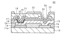
- FIG. 15 is a schematic cross-sectional view showing an example of the structure of the portion of the conventional active matrix substrate 60 where the TFT 61 is formed.
- a gate electrode 11 a (which forms a part of the gate wiring 11) and a capacitor wiring 13 are formed on the glass insulating substrate 10 of the active matrix substrate 60.
- the interlayer insulating film 14 is formed so as to cover the insulating substrate 10.
- the interlayer insulating film 14 is made of an SOG material containing the above-described siloxane composition or the like.
- the portions except for the respective edge portions are not covered with the interlayer insulating film 14, and openings Ca and Ca are formed.
- a gate insulating film 15 is formed on the interlayer insulating film 14, and a semiconductor film 16 is formed on a portion of the gate insulating film 15 corresponding to the opening Ca on the gate electrode 11a side.
- An n + film 17 is formed so as to cover the semiconductor film 16, a source region and a drain region are formed, and a source electrode 18 and a drain electrode 19 are formed on the source region and the drain region.
- the TFT 61 is configured by the gate electrode 11 a, the gate insulating film 15, the semiconductor film 16, the n + film 17, the source electrode 18, and the drain electrode 19.
- a passivation film 21 is formed so as to cover the source electrode 18 and the drain electrode 19, and an interlayer insulating film 22 containing an organic material is formed so as to cover the passivation film 21.
- a capacitor electrode 20 is formed on the gate insulating film 15 in the opening Ca on the capacitor wiring 13 side.
- a pixel electrode 23 is formed in the opening Cb on the capacitor electrode 20.
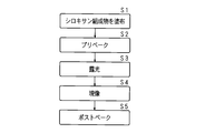
- FIG. 16 is a flowchart showing a processing procedure for forming the interlayer insulating film 14.
- An SOG material is applied on the insulating substrate 10, the gate wiring 11, and the capacitor wiring 13 to form a coating film (S11). After forming the coating film, it is baked to adjust the film thickness (S12). After baking, a photoresist material is applied on the coating film to form a resist (S13).
- a resist pattern is formed by exposing using a photomask (S14) and developing (S15).
- etching such as dry etching is performed using a mixed gas of carbon tetrafluoride and oxygen (S16) to form the opening Ca.
- the resist is peeled off (S17).
- the film strength of the interlayer insulating film made of the above siloxane composition is weak, and when the film stress is generated due to the difference in thermal expansion coefficient at low temperature, the substrate warps and the substrate flow trouble occurs in the manufacturing apparatus. There was a problem.
- the film stress causes problems such as cracks in the film, peeling and distortion in the film, and there is a problem in that the focus shifts in the exposure process and the yield decreases.
- a crack occurs, there is a problem that a defect occurs due to a foreign substance derived from the siloxane composition resulting from the crack.
- the defect occurrence rate is increased due to the by-products generated by etching, the yield is lowered, and the cost is further increased. Since this by-product causes leakage between the wirings, the interlayer insulating film 14 is left in addition to the necessary portions. That is, the opening of the interlayer insulating film 14 includes the portion where the TFT 61 is formed and the capacitor wiring 13. This is limited to a part such as a part where the upper opening Ca is formed, and since the opening area of the interlayer insulating film 14 is small, it causes a decrease in panel transmittance, and a backlight having high luminance to compensate for this. Had to be used.
- the present invention has been made in view of such circumstances, and the formed film has high heat resistance, low temperature curability, high strength, and high crack resistance, and does not cause defects due to substrate warpage and impurities.
- a positive photosensitive siloxane composition having good pattern formability and a resist, so that no by-product is generated, the occurrence of defects is suppressed, the yield is good, and the siloxane is inexpensive.
- An object of the present invention is to provide an active matrix substrate in which an interlayer insulating film made of a composition is formed and has good light transmittance, a display device including the active matrix substrate, and a method for manufacturing the active matrix substrate. .
- the positive photosensitive siloxane composition according to the present invention comprises (I) at least two kinds of polysiloxanes having different dissolution rates in an aqueous solution of tetramethylammonium hydroxide (TMAH), (II) a diazonaphthoquinone derivative, and (III) a photoacid.
- TMAH tetramethylammonium hydroxide
- II a diazonaphthoquinone derivative
- III a photoacid
- R 1 is a linear, branched or cyclic alkyl group having 1 to 20 carbon atoms in which any methylene may be replaced by oxygen, or any hydrogen having 6 to 20 carbon atoms is fluorine.
- R 2 represents an alkyl group having 1 to 5 carbon atoms
- n represents 0 or 1.
- a polysiloxane obtained by hydrolyzing and condensing a silane compound represented by formula (1) in a presence of a basic catalyst is soluble in a 5% by mass TMAH aqueous solution and has a dissolution rate of 1000 kg / sec or less.
- (Ia) (B) The dissolution rate of the pre-baked membrane obtained by hydrolysis and condensation of the silane compound represented by the general formula (1) in the presence of a basic catalyst or an acidic catalyst with respect to an aqueous 2.38 mass% TMAH solution It is characterized by being a mixture with polysiloxane (Ib) which is 100 liters / second or more.
- An active matrix substrate according to the present invention is formed on a substrate so that a plurality of source lines and a plurality of gate lines cross three-dimensionally, and in the vicinity of a portion where the source lines and the gate lines cross each other, a thin film transistor A pixel electrode electrically connected to a corresponding source wiring through the thin film transistor, and at least between the source wiring and the gate wiring, An interlayer insulating film made of a cured product of the siloxane composition is interposed.
- a display device includes any one of the active matrix substrates described above, a display medium layer disposed on the active matrix substrate, and a counter substrate facing the active matrix substrate via the display medium layer. It is characterized by providing.
- a plurality of source wirings and a plurality of gate wirings are three-dimensionally crossed on a substrate, and the source wiring and the gate wiring cross each other.
- Forming a thin film transistor in the vicinity and forming a pixel electrode electrically connected to a corresponding source wiring through the thin film transistor, and at least one of the above-mentioned between the source wiring and the gate wiring A method of manufacturing an active matrix substrate having an interlayer insulating film forming step of forming an interlayer insulating film made of a cured product of the positive photosensitive siloxane composition, wherein the interlayer insulating film forming step includes the positive photosensitive siloxane
- the formed film has high heat resistance, low temperature curability, high strength, and high crack resistance. And, the solubility in an alkali developer is good, and the film is melted at a low viscosity due to high temperature before the pattern is fully cured, so that patterns such as holes and lines obtained after development flow, so-called “Pattern dripping” does not occur, and the pattern formability is good.
- the active matrix substrate of the present invention without using a resist, no by-product is generated, occurrence of defects is suppressed, an interlayer insulating film is formed at a low cost with a good yield, The transmittance is good.
- the transmittance is good.
- the resist coating process, the etching process, and the resist stripping process are unnecessary when patterning after forming the film containing the siloxane composition, thereby reducing the manufacturing cost. be able to. Further, by eliminating the etching process, generation of by-products is eliminated, the defect occurrence rate is reduced, and the yield is good.
- FIG. 3 is a schematic cross-sectional view showing a portion where a gate wiring and a source wiring of the active matrix substrate according to Embodiment 1 of the present invention intersect. It is typical sectional drawing which shows the manufacturing process of the manufacturing method of the active matrix substrate which concerns on Embodiment 1 of this invention.
- the positive type photosensitive siloxane composition according to the present invention comprises at least two types of (I) polysiloxanes having different solubility in an aqueous TMAH solution, and (II) diazonaphthoquinone. A derivative, (III) a photoacid generator, and (IV) a solvent.
- silsesquioxane having a silanol group as a crosslinking point is preferable.
- a silanol group forms a siloxane bond by heating, and can impart high heat resistance.
- Silsesquioxane is preferable because it is excellent in low-temperature curing and pattern stability.
- Silsesquioxanes called saddle type and ladder type are more preferable because of high crack resistance.
- Silicone resin has high crack resistance, but is too flexible, and thus is not preferable as a material for an interlayer insulating film. Also, the thermal stability of the pattern shape is inferior.
- saddle-type silsesquioxane and ladder-type silsesquioxane have a low solubility in an alkali developer because they have few free silanol groups. Accordingly, as the photosensitive composition, a siloxane having a low solubility in an alkali developer and a siloxane having a high solubility in an alkali developer are used in combination.
- Examples of the two types of polysiloxane include the following polysiloxane (Ia) and polysiloxane (Ib).
- TMAH aqueous solution a pre-baked film obtained by hydrolysis and condensation of a silane compound represented by the following formula (1) in the presence of a basic catalyst is soluble in a 5% by mass TMAH aqueous solution, Its solubility is 1000 kg / sec or less.
- R 1 n Si (OR 2 ) 4-n (In the formula, R 1 is a linear, branched or cyclic alkyl group having 1 to 20 carbon atoms in which any methylene may be replaced by oxygen, or any hydrogen having 6 to 20 carbon atoms is fluorine. Represents an aryl group which may be substituted, R 2 represents an alkyl group having 1 to 5 carbon atoms, and n represents 0 or 1.
- the solubility in an aqueous solution is 100 kg / second or more.
- the dissolution rate of the polysiloxanes (Ia) and (Ib) in the TMAH aqueous solution is measured and calculated as follows. First, polysiloxane is diluted with propylene glycol monomethyl ether acetate (PGMEA) so as to be about 35% by mass and dissolved. This solution is spin-coated on a silicon wafer to a dry film thickness of about 2 ⁇ m, and then heated on a hot plate at 100 ° C. for 60 seconds to remove the solvent. The film thickness of the coating film is measured with a spectroscopic ellipsometer (manufactured by Woollam).
- PGMEA propylene glycol monomethyl ether acetate
- the silicon wafer having this film was immersed in a 5% TMAH aqueous solution for polysiloxane (Ia) and a 2.38% TMAH aqueous solution for polysiloxane (Ib) at room temperature (25 ° C.), and the coating disappeared. The time to do was measured. The dissolution rate is determined by dividing the initial film thickness by the time until the film disappears. When the dissolution rate is extremely slow, the film thickness is measured after being immersed for a certain time, and the dissolution rate is calculated by dividing the change in film thickness before and after the immersion by the immersion time.
- the polystyrene-reduced mass average molecular weight is preferably 700 to 10,000, more preferably 1,000 to 4,000.
- the molecular weight is too large, there is a problem that sufficient resolution cannot be obtained with a development residue or the like and the sensitivity is lowered. Therefore, it is preferable to adjust the alkali dissolution rate so that the molecular weight does not increase.
- the mixing ratio of polysiloxane (Ia) and (Ib) can be adjusted at any ratio depending on the film thickness of the interlayer insulating film, the sensitivity of the photosensitive composition, the resolution, etc., but the polysiloxane (Ia ) In an amount of 20% by mass or more is preferable because the “pattern” dripping prevention effect during heat curing is good.
- the siloxane composition according to the present invention contains a diazonaphthoquinone derivative, so that the exposed portion becomes soluble in an alkali developer and constitutes a positive type that is removed by development.
- the diazonaphthoquinone derivative according to the present invention is a compound in which naphthoquinone diazide sulfonic acid is ester-bonded to a compound having a phenolic hydroxyl group, and the structure is not particularly limited, but is an ester with a compound having one or more phenolic hydroxyl groups Preferably it is a compound.
- 4-naphthoquinone diazide sulfonic acid or 5-naphthoquinone diazide sulfonic acid can be used. Since 4-naphthoquinonediazide sulfonic acid ester compound has absorption in the i-line (wavelength 365 nm) region, it is suitable for i-line exposure. Further, the 5-naphthoquinonediazide sulfonic acid ester compound has absorption in a wide wavelength range and is therefore suitable for exposure in a wide wavelength range.
- a 4-naphthoquinone diazide sulfonic acid ester compound or a 5-naphthoquinone diazide sulfonic acid ester compound depending on the wavelength to be exposed. It is also possible to use a mixture of a 4-naphthoquinone diazide sulfonic acid ester compound and a 5-naphthoquinone diazide sulfonic acid ester compound. Although it does not specifically limit as a compound which has a phenolic hydroxyl group, For example, the following compounds are mentioned (Honshu Chemical Industry Co., Ltd. product name addition).
- the preferred addition amount of the diazonaphthoquinone derivative is determined by the esterification rate of naphthoquinone diazide sulfonic acid, the physical properties of the polysiloxane used, the required sensitivity, the dissolution contrast between the exposed and unexposed areas, etc.
- the use of the interlayer insulating film of the present invention is preferably 3 parts by mass or more and 10 parts by mass or less, more preferably 5 parts by mass or more and 7 parts by mass or less with respect to 100 parts by mass of polysiloxane (I).
- the addition amount of the diazonaphthoquinone derivative is less than 3 parts by mass, the dissolution contrast between the exposed part and the unexposed part is too low, and there is no realistic photosensitivity.
- the amount is preferably 5 parts by mass or more.
- the addition amount of the diazonaphthoquinone derivative is more than 10 parts by mass, it is confirmed by experiments that coloring due to decomposition of the quinonediazide compound caused by thermal curing or thermal history becomes remarkable and the colorless transparency of the cured film is lowered. Yes. Furthermore, the thermal decomposition may cause deterioration of the electrical insulation of the cured product and release of gas, which may cause a problem in the subsequent process.
- the siloxane composition according to the present invention contains a photoacid generator.
- the photoacid generator When exposed to radiation, the photoacid generator decomposes and releases an acid that promotes condensation of silanol groups.
- the radiation include visible light, ultraviolet rays, infrared rays, X-rays, electron beams, ⁇ rays, or ⁇ rays.
- those that generate acid by ultraviolet rays used in the production of thin film transistors are preferred.
- a preferable addition amount of the photoacid generator is determined by the kind of the active substance generated by decomposition, the generation amount, the required sensitivity, the dissolution contrast between the exposed portion and the unexposed portion, and the like. ) Preferably it is 0.01 mass part or more and 10 mass parts or less with respect to 100 mass parts, More preferably, it is 0.1 mass part or more and 5 mass parts or less. When the addition amount is less than 0.01 parts by mass, there may be no addition effect. On the other hand, when the addition amount is more than 10 parts by mass, cracks may occur in the formed film, or coloring due to decomposition products may become remarkable, and the colorless transparency of the film may decrease.
- the thermal insulation will deteriorate the electrical insulation of a hardened
- the photoacid generator is contained in an amount of 0.01 parts by weight or more and 10 parts by weight or less with respect to 100 parts by weight of the polysiloxane (I), the acid generated after the light irradiation promotes the condensation reaction of silanol in the polysiloxane at a low temperature. It is possible to achieve high resolution with no pattern sagging.
- photoacid generator examples include diazomethane compounds, diphenyliodonium salts, triphenylsulfonium salts, sulfonium salts, ammonium salts, phosphonium salts, sulfonimide compounds and the like.
- the structure of these photoacid generators can be represented by the general formula (2).
- R + is an organic ion selected from the group consisting of an alkyl group, an aryl group, an alkenyl group, an acyl group, and an alkoxyl group modified with hydrogen, a carbon atom, or other hetero atom, such as diphenyliodonium ion, triphenyl Represents a sulfonium ion.
- X ⁇ is preferably any counter ion represented by the following general formula.
- Y is a halogen atom
- R a is an alkyl group having 1 to 20 carbon atoms or an aryl having 6 to 20 carbon atoms substituted with a substituent selected from fluorine, nitro group, and cyano group
- R b is hydrogen or an alkyl group having 1 to 8 carbon atoms
- p is a number from 0 to 6
- q is a number from 0 to 4.
- Specific counter ions include BF 4 ⁇ , (C 6 F 5 ) 4 B ⁇ , ((CF 3 ) 2 C 6 H 3 ) 4 B ⁇ , PF 6 ⁇ , (CF 3 CF 2 ) 3 PF 3 ⁇ .
- those that generate sulfonic acids or boric acids are particularly preferable.
- tricumyliodonium tetrakis (pentafluorophenyl) boric acid Rhodia Co., Ltd., “PHOTOINITIATOR 2074” (trade name)
- Diphenyliodonium tetra (perfluorophenyl) boric acid Diphenyliodonium tetra (perfluorophenyl) boric acid
- a cation portion composed of a sulfonium ion
- anion portion composed of a pentafluoroborate ion.
- triphenylsulfonium trifluoromethanesulfonic acid triphenylsulfonium camphorsulfonic acid, triphenylsulfonium tetra (perfluorophenyl) boric acid, 4-acetoxyphenyldimethylsulfonium hexafluoroarsenic acid, 1- (4-n-butoxynaphthalene- 1-yl) tetrahydrothiophenium trifluoromethanesulfonic acid, 1- (4,7-dibutoxy-1-naphthalenyl) tetrahydrothiophenium trifluoromethanesulfonic acid, diphenyliodonium trifluoromethanesulfonic acid, diphenyliodonium hexafluoroarsenic acid, etc.
- a photoacid generator represented by the following formula can also be used.
- each A independently represents an alkyl group having 1 to 20 carbon atoms, an alkoxy group having 1 to 20 carbon atoms, an aryl group having 6 to 20 carbon atoms, an alkylcarbonyl group having 1 to 20 carbon atoms, or 6 to 6 carbon atoms.
- B- is a fluorinated alkylsulfonate group, a fluorinated aryl Examples thereof include a sulfonate group, a fluorinated alkyl borate group, an alkyl sulfonate group, and an aryl sulfonate group.
- a compound obtained by exchanging the cation and anion shown in these formulas with each other, and a photoacid generator combining the cation or anion shown in these formulas with the above-mentioned various cations or anions can also be used. .
- a combination of any of the sulfonium ions represented by the formula and a tetra (perfluorophenyl) borate ion a combination of any of the iodonium ions represented by the formula and a tetra (perfluorophenyl) borate ion Those can also be used as photoacid generators.
- solvent examples include ethylene glycol monoalkyl ethers such as ethylene glycol monomethyl ether, ethylene glycol monoethyl ether, ethylene glycol monopropyl ether, and ethylene glycol monobutyl ether, diethylene glycol dimethyl ether, diethylene glycol diethyl ether, and diethylene glycol dipropyl ether.
- ethylene glycol monoalkyl ethers such as ethylene glycol monomethyl ether, ethylene glycol monoethyl ether, ethylene glycol monopropyl ether, and ethylene glycol monobutyl ether, diethylene glycol dimethyl ether, diethylene glycol diethyl ether, and diethylene glycol dipropyl ether.
- Diethylene glycol dialkyl ethers such as diethylene glycol dibutyl ether, ethylene glycol alkyl ether acetates such as methyl cellosolve acetate and ethyl cellosolve acetate, propylene glycol monomethyl ether acetate (PGMEA), propylene glycol monoethyl ether acetate, propylene glycol Propylene glycol alkyl ether acetates such as nopropyl ether acetate, aromatic hydrocarbons such as benzene, toluene, xylene, ketones such as methyl ethyl ketone, acetone, methyl amyl ketone, methyl isobutyl ketone, cyclohexanone, ethanol, propanol, butanol, Examples thereof include alcohols such as hexanol, cyclohexanol, ethylene glycol, and glycerin, esters such as ethyl 3-e
- the formed film has high heat resistance, low temperature curability, high strength, and high crack resistance. And the solubility with respect to an alkali developing solution is good, pattern dripping does not occur, and the pattern formability is good.
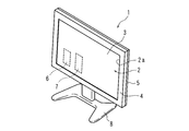
- FIG. 1 is a schematic perspective view showing a television receiver (hereinafter referred to as a TV receiver) 1 according to Embodiment 1 of the present invention
- FIG. 2 is a schematic sectional view showing a display panel 3 according to Embodiment 1.
- FIG. 3 is a schematic plan view showing a pixel of the active matrix substrate 30 according to Embodiment 1
- FIG. 4 is a schematic cross-sectional view showing a portion of the active matrix substrate 30 where the TFT 25 is provided
- FIG. 5 is an active matrix.
- 3 is a schematic cross-sectional view showing a portion where a gate wiring 11 and a source wiring 12 cross a substrate 30.
- FIG. 1 is a schematic perspective view showing a television receiver (hereinafter referred to as a TV receiver) 1 according to Embodiment 1 of the present invention
- FIG. 2 is a schematic sectional view showing a display panel 3 according to Embodiment 1.
- FIG. 3 is a schematic plan view showing a pixel of the active matrix
- the TV receiver 1 includes a horizontally long display module 2 that displays video, a tuner 6 that receives broadcast waves from an antenna (not shown), and a decoder 7 that decodes encoded broadcast waves.
- the TV receiver 1 decodes the broadcast wave received by the tuner 6 by the decoder 7 and displays an image on the display module 2 based on the decoded information.
- a stand 8 that supports the TV receiver 1 is provided below the TV receiver 1.
- the display module 2 when the display module 2 is an edge light type, the display module 2 includes a display panel 3, for example, three optical sheets (hereinafter, not shown), a light guide plate, a reflection sheet, and a chassis.
- the display module 2 is accommodated in a vertical posture in a front cabinet 4 and a rear cabinet 5 that are arranged in a vertical posture in the front-rear direction.
- the front cabinet 4 is a rectangular frame that covers the peripheral edge of the display module 2, and has a rectangular opening 2a in the center.
- the front cabinet 4 is made of, for example, a plastic material.
- the rear cabinet 5 has a rectangular tray shape with the front side open, and is made of, for example, a plastic material. In addition, you may comprise the front cabinet 4 and the back cabinet 5 from another material.
- the vertical and horizontal dimensions of the front cabinet 4 and the rear cabinet 5 are substantially the same, and the peripheral portions of each other face each other.
- the vertical and horizontal dimensions of the display panel 3 are slightly larger than the opening 2 a of the front cabinet 4, and the peripheral portion of the display panel 3 faces the inner edge portion of the front cabinet 4.
- the display panel 3 includes an active matrix substrate 30 and a counter substrate (color filter substrate) 31 facing each other, a liquid crystal layer 32 provided as a display medium layer between the active matrix substrate 30 and the counter substrate 31, and an active matrix substrate 30. And a sealing material 33 provided in a frame shape for adhering the counter substrate 31 to each other and enclosing the liquid crystal layer 32 between the active matrix substrate 30 and the counter substrate 31.
- the active matrix substrate 30 is provided between a plurality of gate wirings 11 provided on the insulating substrate 10 such as a glass substrate so as to extend in parallel with each other, and the gate wirings 11 respectively.
- a plurality of capacitance lines 13 extending in parallel with each other; a plurality of source lines 12 provided so as to extend in parallel with each other in a direction crossing each gate line 11; and each crossing portion of each gate line 11 and each source line 12; That is, a plurality of TFTs 25 provided for each pixel, a plurality of pixel electrodes 23 provided in a matrix and connected to each TFT 25, and an alignment film (not shown) provided so as to cover each pixel electrode 23 ).
- an interlayer insulating film 14 and a gate are formed in a portion including a gate wiring 11, a capacitor wiring 13, and a crossing portion of the gate wiring 11 and the source wiring 12 below the source wiring 12 of the active matrix substrate 30.
- An insulating film 15 is interposed.
- the interlayer insulating film 14 is formed using a cured product of the siloxane composition of the present invention.
- the siloxane composition is a material having heat resistance against the thermal history of the subsequent process. For example, even if it receives the thermal history in the film forming process of the gate insulating film 15, it does not cause a change in physical properties that causes a problem in device characteristics. In order to withstand the thermal history of the film formation process of the gate insulating film 15, it is preferable to have heat resistance of 300 ° C. or higher.
- the heat resistance is a temperature at which stability of the electrical insulation, dielectric constant, coloring of the transparent film, whitening, film thickness, etc. can be maintained after the curing process of the siloxane composition and the heat history exposed after the curing process. Defined by That is, the physical properties are retained after receiving a thermal history.
- the light transmittance (transmittance) of the interlayer insulation film 14 can ensure 90% or more.
- the light transmittance is a film of 2 ⁇ m in wavelength of 400 nm after applying a heat history at 300 ° C. for 1 hour to a film after being cured at a temperature of 300 ° C. or less on a glass substrate. It is defined as the transmittance with respect to the thickness.
- the relative dielectric constant of the interlayer insulating film 14 is preferably 4 or less.
- the cured film is reduced in film thickness due to the heat history (film thickness ) Is desirable. That is, the film slip at 300 ° C. is preferably 5% or less.
- a passivation film 21 is formed so as to cover the source wiring 12, and an interlayer insulating film 22 containing an organic material is formed so as to cover the passivation film 21 and be flattened.
- a pixel electrode 23 is patterned on the interlayer insulating film 22.
- a gate electrode 11 a (which forms part of the gate wiring 11) and a capacitor wiring 13 are formed on the insulating substrate 10 of the active matrix substrate 30.
- the interlayer insulating film 14 is formed so as to cover the insulating substrate 10.
- portions other than the respective edge portions are not covered with the interlayer insulating film 14, and openings Ca and Ca are formed.
- a gate insulating film 15 is formed on the interlayer insulating film 14, the gate electrode 11a, and the capacitor wiring 13, and the semiconductor film 16 is formed on the gate insulating film 15 at a portion corresponding to the opening Ca on the gate electrode 11a side. Is formed.
- n + film 17 is formed so as to cover the semiconductor film 16, a source region and a drain region are formed, and a source electrode 18 and a drain electrode 19 are formed on the source region and the drain region.
- the gate electrode 11 a, the gate insulating film 15, the semiconductor film 16, the n + film 17, the source electrode 18, and the drain electrode 19 constitute a TFT 25.
- a passivation film 21 is formed so as to cover the source electrode 18 and the drain electrode 19, and an interlayer insulating film 22 is formed so as to cover the passivation film 21.
- a capacitor electrode 20 is formed at a position corresponding to the capacitor wiring 13 on the gate insulating film 15.
- a pixel electrode 23 is formed on the capacitor electrode 20.
- the pixel electrode 23 is connected to the capacitor electrode 20 in the opening Cb above the opening Ca, and the capacitor electrode 20 overlaps the capacitor wiring 13 through the gate insulating film 15 to form an auxiliary capacitor.
- the capacitor electrode 20 is connected to the drain electrode 19 by a drain wiring 27.
- FIGS. 7F to 7H are schematic cross-sectional views illustrating manufacturing steps of the method for manufacturing the active matrix substrate 30 according to the present embodiment.
- a titanium film thickness of about 50 nm
- an aluminum film thickness of about 200 nm
- a titanium film thickness of about 100 nm
- the gate wiring the portion to be the gate electrode 11a is also formed
- the capacitor wiring 13 is formed (FIG. 6A).
- the metal film is not limited to the above three-layer structure, and may be a Cu film or the like.
- FIG. 8 is a flowchart showing a processing procedure for forming the interlayer insulating film.
- the siloxane composition according to the present invention is applied onto the substrate 10 including the gate wiring 11 and the capacitor wiring 13 by spin coating to form a film 14a (S1, FIG. 6B).
- the film thickness is adjusted by pre-baking, for example, at 100 ° C. for 90 seconds (S2).
- pre-baking the film 14a is exposed using the photomask 26 (S3, FIG. 6C).
- development is performed with a 2.38% TMAH aqueous solution (S4).
- S4 TMAH aqueous solution
- post-baking is performed at 250 ° C., for example, and the film 14a is cured to obtain the interlayer insulating film 14 (S5, FIG. 6D).
- a gate insulating film 15 is formed by forming and patterning a film using, for example, silicon oxide or silicon nitride by a CVD (Chemical Vapor Deposition) method.
- the interlayer insulating film 14 has a heat resistance of 300 ° C. or higher, and does not change its physical properties even when it receives a thermal history of the film forming process of the gate insulating film 15.
- a film made of amorphous silicon or the like or a film made of n + amorphous silicon or the like is formed by, for example, CVD, and patterned to form a semiconductor film 16 and an n + film 17 corresponding to the source region and the drain region.
- a film made of amorphous silicon or the like or a film made of n + amorphous silicon or the like is formed by, for example, CVD, and patterned to form a semiconductor film 16 and an n + film 17 corresponding to the source region and the drain region.
- Mo or the like is deposited by sputtering and patterned to form the source electrode 18 and the drain electrode 19 (FIG. 7F).
- the capacitor electrode 20 is formed on a portion of the gate insulating film 15 corresponding to the opening Ca on the capacitor wiring 13 side (not shown).
- a film such as silicon nitride is formed on the source electrode 18 and the drain electrode 19 by, for example, a CVD method, and a passivation film 21 is formed by patterning, and a film made of a synthetic resin such as an acrylic resin is formed on the passivation film 21.
- the interlayer insulating film 22 is formed by patterning (FIG. 7G).
- An ITO film is formed on the interlayer insulating film 22 by, for example, sputtering, and patterned to form the pixel electrode 23 (FIG. 7H).
- the manufacturing process can be simplified. Substrate warpage due to film stress is also suppressed, and occurrence of substrate flow troubles during manufacturing is also suppressed. In addition, by-product (foreign matter) is not generated due to the elimination of the etching step, crack resistance is good, and foreign matter derived from the siloxane composition is not generated, so that the defect occurrence rate is reduced and the yield is improved. Therefore, the manufacturing cost can be reduced.
- the transmittance of the interlayer insulating film 14 is 90% or more, and the transmittance of the display panel 3 including the active matrix substrate 30 having the interlayer insulating film 14 is good.
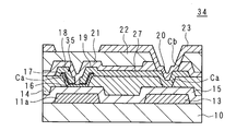
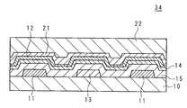
- FIG. The display module according to Embodiment 2 of the present invention is the same as the display module 2 according to Embodiment 1 except that the order of film formation of the interlayer insulating film 14 and the gate insulating film 15 of the active matrix substrate 34 is different. It has the composition of. 9 is a schematic cross-sectional view showing a portion of the active matrix substrate 34 where the TFT 35 is provided, and FIG. 10 is a schematic cross-sectional view showing a portion where the gate wiring 11 and the source wiring 12 of the active matrix substrate 34 intersect. . 9 and 10, the same parts as those in FIGS. 4 and 5 are denoted by the same reference numerals, and detailed description thereof is omitted.
- a gate insulating film is formed between the gate wiring 11 formed on the insulating substrate 10 and the source wiring 12 at the intersection of the gate wiring 11 and the source wiring 12 of the active matrix substrate 34.
- 15 and the interlayer insulating film edge film 14 are interposed in this order from the insulating substrate 10 side.
- the interlayer insulating film 14 is made of an SOG material having a siloxane composition according to the present invention similar to the above.
- the gate electrode 11 a and the capacitor wiring 13 are formed on the insulating substrate 10 of the active matrix substrate 34.
- the gate insulating film 15 is formed so as to cover the insulating substrate 10, the gate wiring 11 including the gate electrode 11 a, and the capacitor wiring 13.
- the interlayer insulating film 14 is formed so as to cover the gate insulating film 15. Openings Ca and Ca are formed in portions of the interlayer insulating film 14 corresponding to the gate electrode 11 a and the capacitor wiring 13.
- a semiconductor film 16 and an n + film 17 are formed in this order in the opening Ca on the gate electrode 11 a side of the interlayer insulating film 14.
- the resist coating process, the etching process, and the resist stripping process are unnecessary when patterning after forming the film 14a containing the siloxane composition according to the present invention, thereby reducing the manufacturing cost.
- by eliminating the etching process generation of by-products is eliminated and crack resistance is good, so that no foreign matter derived from the siloxane composition is produced, the defect rate is reduced, and the yield is improved.
- the transmittance of the interlayer insulating film 14 is 90% or more, and the transmittance of the display panel 3 is good.
- FIG. 11 is a schematic cross-sectional view showing a portion of the active matrix substrate 36 where the TFT 37 is provided.
- the configuration of the portion where the gate wiring 11 and the source wiring 12 intersect is the same as the configuration of the portion where the gate wiring 11 and the source wiring 12 according to the second embodiment intersect.
- the same parts as those in FIG. 11 are the same parts as those in FIG.
- the gate electrode 11 a and the capacitor wiring 13 are formed on the insulating substrate 10 of the active matrix substrate 36.
- the gate insulating film 15 is formed so as to cover the insulating substrate 10, the gate wiring 11 including the gate electrode 11 a, and the capacitor wiring 13.
- a semiconductor film 16 and an n + film 17 are formed in this order on a portion of the gate insulating film 15 corresponding to the gate electrode 11a.
- the interlayer insulating film 14 is formed so as to cover the gate insulating film 15. Openings Ca and Ca are formed in portions of the interlayer insulating film 14 corresponding to the gate electrode 11 a and the capacitor wiring 13.
- the resist coating process, the etching process, and the resist stripping process are unnecessary when patterning after forming the film 14a containing the siloxane composition according to the present invention, thereby reducing the manufacturing cost.
- by eliminating the etching process generation of by-products is eliminated and crack resistance is good, so that no foreign matter derived from the siloxane composition is produced, the defect rate is reduced, and the yield is improved.
- the transmittance of the interlayer insulating film 14 is 90% or more, and the transmittance of the display panel 3 is good.
- FIG. 12 is a schematic cross-sectional view showing a portion of the active matrix substrate 38 where the TFT 39 is provided.
- the configuration of the portion where the gate wiring 11 and the source wiring 12 intersect is the same as the configuration of the portion where the gate wiring 11 and the source wiring 12 according to the first embodiment intersect.
- the interlayer insulating film 22 is formed using a siloxane composition similar to that of the interlayer insulating film 14, not an acrylic resin. Therefore, in the present embodiment, the material of the film constituting the active matrix substrate 38 and the film forming equipment can be shared, the manufacturing cost can be reduced, and the management of the material is facilitated. be able to.
- FIG. 5 The display device according to the fifth embodiment of the present invention has the same configuration as the display device according to the second embodiment, except that the formation pattern of the interlayer insulating film 14 is different in the active matrix substrate 40.
- 13 is a schematic cross-sectional view showing a portion of the active matrix substrate 40 where the TFT 41 is provided
- FIG. 14 is a schematic cross-sectional view showing a portion where the gate wiring 11 and the source wiring 12 of the active matrix substrate 40 intersect.
- 13 and 14 the same parts as those in FIGS. 9 and 10 are denoted by the same reference numerals, and detailed description thereof is omitted.
- a gate insulating film is formed between the gate wiring 11 formed on the insulating substrate 10 and the source wiring 12 at the intersection of the gate wiring 11 and the source wiring 12 of the active matrix substrate 40.
- 15 and the interlayer insulating film edge film 14 are interposed in this order from the insulating substrate 10 side.
- the interlayer insulating film 14 is made of the same siloxane composition according to the present invention as described above.
- the interlayer insulating film 14 is not formed on the gate insulating film 15 corresponding to between the gate wirings 11 and 11. Further, as will be described later, the interlayer insulating film 14 is not formed above the portion of the gate wiring 11 where the gate electrode 11a is formed.
- the gate electrode 11 a and the capacitor wiring 13 are formed on the insulating substrate 10 of the active matrix substrate 40.
- the interlayer insulating film 14 is not formed above the portion of the gate wiring 11 where the gate electrode 11a is formed. Further, the interlayer insulating film 14 is not formed on the upper side of the capacitor wiring 13 and between the gate wiring 11 and the capacitor wiring 13.
- the interlayer insulating film 14 can be formed without performing an etching step, and a by-product based on the siloxane composition is formed. Since no generation occurs and the occurrence of leakage between wirings is suppressed, the interlayer between only the minimum necessary parts where the inter-wiring capacitance is required to be reduced, such as the crossing part of the gate wiring 11 and the source wiring 12 An insulating film 14 can be provided.
- the display having the active matrix substrate 40 is designed by not designing the interlayer insulating film 14 in the pixel portion where the transmittance is to be ensured, the capacitance wiring portion 13 where the capacitance is to be increased, and the openings Ca and Ca portions.
- the panel 3 can have good transmittance.
- the mixed solution was dropped into the flask at 10 ° C., stirred at the same temperature for 3 hours, and neutralized by adding a 10% HCl aqueous solution.
- a 10% HCl aqueous solution 400 ml of toluene and 100 ml of water were added, and the mixture was separated into two layers. The resulting organic layer was concentrated under reduced pressure to remove the solvent, and propylene was added to the concentrate so that the solid concentration was 40% by mass.
- Glycol monomethyl ether acetate (PGMEA) was added and adjusted.
- Mw mass average molecular weight
- the obtained resin solution is applied to a silicon wafer by a spin coater so that the film thickness after pre-baking is 2 ⁇ m, and the dissolution rate in a 5% TMAH aqueous solution after pre-baking (hereinafter sometimes abbreviated as “ADR”).
- ADR dissolution rate in a 5% TMAH aqueous solution after pre-baking
- the photosensitive siloxane composition 1 was obtained by adjusting the solid content to 35% with a mixed solvent
- This photosensitive siloxane composition 1 was applied onto a silicon wafer by spin coating, and after application, pre-baked at 100 ° C. on a hot plate to adjust the film thickness to 2.3 ⁇ m.
- NA 0.1: manufactured by Nikon Co., Ltd.
- TMAH TMAH aqueous solution at room temperature.
- rinsing with pure water was performed.
- PPA-501F manufactured by Canon Inc.
- a cured film was prepared by curing for 30 minutes at 230 ° C. in air using a hot plate.
- the final film thickness after curing was 2.1 ⁇ m.
- SEM observation confirmed that the 3 ⁇ m contact hole (opening) pattern, which is the resolution limit of the “FX-604” device, was missing.
- whether or not a contact hole can be formed was determined by forming a bottom contact of 80% or more of the mask contact hole design.
- a test specimen for measuring transmittance was prepared by the following procedure.
- the siloxane composition 1 was applied onto glass (“Eagle XG”, thickness 0.7 mm: manufactured by Corning) by spin coating, and after application, pre-baked at 100 ° C. on a hot plate to a film thickness of 2.3 ⁇ m. It was adjusted to become.
- a cured film was prepared by curing for 30 minutes at 230 ° C. in air using a hot plate. Then, the heat history for 1 hour was added at 300 degreeC in the air using the hotplate. When the average film thickness after curing and after the thermal history were determined by SEM observation, there was no change at 2.10 ⁇ m (no film slippage).
- the light transmittance was measured by using “U-4000” (manufactured by Hitachi High-Technologies Corporation) as a spectrophotometer and measuring only the glass as a reference. Next, a specimen for measuring transmittance was measured, and the light transmittance at a wavelength of 400 nm per 2 ⁇ m thickness was determined to be 97%.
- Example 2 (positive photosensitive siloxane composition 2)> A photosensitive siloxane composition 2 was obtained in the same manner as in Example 1 except that PAC was changed from 6% by mass to 9% by mass with respect to polysiloxane. When applied to the substrate in the same manner as in Example 1 to form a pattern and the resolution of the pattern was confirmed, it was confirmed that the 5 ⁇ m contact hole pattern was removed without residue. Further, the light transmittance was measured in the same manner as in Example 1, and the light transmittance at a wavelength of 400 nm per 2 ⁇ m thickness was determined to be 92%. Further, when the average film thickness was determined in the same manner as in Example 1, it decreased from 2.17 ⁇ m to 2.10 ⁇ m, and the film slip was 3.2%.
- ⁇ Comparative Example 2 (Positive Photosensitive Siloxane Composition 4)> A photosensitive siloxane composition 4 was obtained in the same manner as in Example 1 except that PAG was not added and PAC was changed from 6% by mass to 12% by mass with respect to the polysiloxane. In the same manner as in Example 1, it was applied to a substrate to form a pattern, and when the resolution of the pattern was confirmed, it was confirmed that a 5 ⁇ m contact hole pattern was missing. The light transmittance was measured in the same manner as in Example 1, and the light transmittance at a wavelength of 400 nm per 2 ⁇ m thickness was determined to be 87%. Further, when the average film thickness was determined in the same manner as in Example 1, it decreased from 2.17 ⁇ m to 2.09 ⁇ m, and the film slip was 3.7%.
- Example 1 Comparative Example 1 and Comparative Example 2
- the positive photosensitive siloxane compositions of Examples 1 and 2 have good heat resistance, and have high sensitivity and high definition. It was confirmed that can be formed.
- Embodiments 1 to 5 described above, and various modifications can be made within the scope indicated in the claims.
- embodiments obtained by combining technical means appropriately modified within the scope of the claims are also included in the technical scope of the present invention.
- Display module (display device) 3.
- Display panel (display device) 30, 34, 36, 38, 40 Active matrix substrate 10
- Insulating substrate 11
- Gate wiring 11a
- Source wiring 13
- Capacitance wiring 14
- Interlayer insulating film 15
- Gate insulating film 16
- Semiconductor film 17
- n + film 18
- Drain electrode 20
- Capacity Electrode 21
- Passivation film 22
- Interlayer insulation film 23
- Pixel electrode 25 35, 37, 39, 41 TFT Ca, Cb opening 31 counter substrate 32 liquid crystal layer
Landscapes
- Physics & Mathematics (AREA)
- General Physics & Mathematics (AREA)
- Chemical & Material Sciences (AREA)
- Nonlinear Science (AREA)
- Spectroscopy & Molecular Physics (AREA)
- Engineering & Computer Science (AREA)
- Microelectronics & Electronic Packaging (AREA)
- Optics & Photonics (AREA)
- Crystallography & Structural Chemistry (AREA)
- Mathematical Physics (AREA)
- Chemical Kinetics & Catalysis (AREA)
- Medicinal Chemistry (AREA)
- Polymers & Plastics (AREA)
- Organic Chemistry (AREA)
- Health & Medical Sciences (AREA)
- Power Engineering (AREA)
- Condensed Matter Physics & Semiconductors (AREA)
- Ceramic Engineering (AREA)
- Computer Hardware Design (AREA)
- Materials For Photolithography (AREA)
- Liquid Crystal (AREA)
- Formation Of Insulating Films (AREA)
- Thin Film Transistor (AREA)
- Exposure And Positioning Against Photoresist Photosensitive Materials (AREA)
Abstract
Description
特許文献1においては、シロキサン組成物として具体的には、シロキサンオリゴマー及び空隙形成材を有機溶剤に均一に溶解してなる組成物(特許文献2)、
及び一般式:
(HR2 SiO1/2 )x (SiO4/2 )1.0
(式中、Rは水素原子、アルキル基およびアリール基からなる群から選択される基であり、Xは0.1≦X≦2.0である。)で示されるケイ素樹脂を主剤としてなる組成物(特許文献3)が挙げられている。
図15に示すように、アクティブマトリクス基板60のガラス製の絶縁基板10上に、ゲート電極11a(ゲート配線11の一部をなす)、及び容量配線13が形成されている。
層間絶縁膜14は絶縁基板10を覆うように形成されている。層間絶縁膜14は、上述のシロキサン組成物等を含むSOG材料からなる。ゲート電極11a上、及び容量配線13上で、夫々の端縁部を除く部分は層間絶縁膜14により覆われず、開口部Ca,Caが形成されている。層間絶縁膜14上にはゲート絶縁膜15が形成され、ゲート絶縁膜15上の、ゲート電極11a側の開口部Caに対応する部分に半導体膜16が形成されている。そして、半導体膜16を覆うようにn+ 膜17が形成され、ソース領域及びドレイン領域が形成されており、ソース領域上及びドレイン領域上にソース電極18及びドレイン電極19が形成されている。ゲート電極11a、ゲート絶縁膜15、半導体膜16、n+ 膜17、ソース電極18、及びドレイン電極19によりTFT61が構成される。
また、容量配線13側の開口部Caにおいて、ゲート絶縁膜15上には、容量電極20が形成されている。容量電極20上の開口部Cbには画素電極23が形成されている。
絶縁基板10、ゲート配線11、及び容量配線13上に、SOG材料を塗布し、塗膜を形成する(S11)。
塗膜を形成した後、ベークし、膜厚を調整する(S12)。
ベーク後、塗膜上にフォトレジスト材料を塗布し、レジストを形成する(S13)。
フォトマスクを用いて露光し(S14)、現像(S15)することにより、レジストパターンを形成する。
次に、レジストで覆われていない塗膜の部分について、例えば四フッ化炭素と酸素との混合ガスを用いてドライエッチング等のエッチングを行い(S16)、開口部Caを形成する。
最後に、レジストを剥離する(S17)。
クラックが生じた場合、これに起因するシロキサン組成物由来の異物により、不良が発生するという問題がある。
(A)下記一般式(1):
R1 nSi(OR2 )4-n
(式中、R1 は、任意のメチレンが酸素で置き換えられてもよい炭素数1~20の直鎖状、分岐状若しくは環状のアルキル基、又は炭素数6~20で任意の水素がフッ素で置き換えられてもよいアリール基を表し、R2 は、炭素数1~5のアルキル基を表し、nは0又は1を表す。)
で表されるシラン化合物を塩基性触媒の存在下で加水分解及び縮合させて得られるプリベーク後の膜が5質量%TMAH水溶液に可溶であり、その溶解速度が1000Å/秒以下であるポリシロキサン(Ia)と、
(B)前記一般式(1)で表されるシラン化合物を塩基性触媒又は酸性触媒の存在下で加水分解及び縮合させて得られるプリベーク後の膜の2.38質量%TMAH水溶液に対する溶解速度が100Å/秒以上であるポリシロキサン(Ib)と
の混合物であることを特徴とする。
1.ポジ型感光性シロキサン組成物
本発明に係るポジ型感光性シロキサン組成物(以下、シロキサン組成物という)は、TMAH水溶液に対する溶解度が異なる少なくとも2種類以上の(I)ポリシロキサン、(II)ジアゾナフトキノン誘導体、(III )光酸発生剤、及び(IV)溶剤を含有する。
高い耐熱性を有するポリシロキサンとして、架橋点としてシラノール基を有するシルセスキオキサンが好ましい。シラノール基は加熱によってシロキサン結合を形成し、高い耐熱性を付与することができる。シルセスキオキサンは、低温硬化及びパターンの安定性に優れているので好ましい。籠型及びラダー型と呼ばれるシルセスキオキサンは、クラック耐性が高いので、より好ましい。シリコーン樹脂は、高いクラック耐性を有するが、柔軟過ぎるため、層間絶縁膜の材料としては好ましくない。また、パターン形状の熱安定性にも劣る。一般に、籠型シルセスキオキサン及びラダー型シルセスキオキサンは、フリーのシラノール基が少ないため、アルカリ現像液に対する溶解性が低い。従って、感光性組成物としては、アルカリ現像液に対する溶解性が低いシロキサンとアルカリ現像液に対する溶解性が高いシロキサンとを組み合わせて使用する。2種のポリシロキサンとして、以下のポリシロキサン(Ia)及びポリシロキサン(Ib)が挙げられる。
R1 nSi(OR2 )4-n
(式中、R1 は、任意のメチレンが酸素で置き換えられてもよい炭素数1~20の直鎖状、分岐状若しくは環状のアルキル基、又は炭素数6~20で任意の水素がフッ素で置き換えられてもよいアリール基を表し、R2 は、炭素数1~5のアルキル基を表し、nは0又は1を表す。)
ポリシロキサン(Ia)及び(Ib)のTMAH水溶液に対する溶解速度は、次のように測定して算出する。
まず、ポリシロキサンをプロピレングリコールモノメチルエーテルアセテート(PGMEA)に35質量%程度になるように希釈し、溶解する。この溶液をシリコンウエハ上に乾燥膜厚が約2μmの厚さになるようにスピンコーティングし、その後100℃のホットプレート上で60秒間加熱して溶剤を除去する。分光エリプソメーター(Woollam社製)で、塗布膜の膜厚測定を行う。次に、この膜を有するシリコンウエハを、ポリシロキサン(Ia)については5%TMAH水溶液、ポリシロキサン(Ib)については、2.38%TMAH水溶液に室温(25℃)で浸漬し、被膜が消失するまでの時間を測定した。溶解速度は、初期膜厚を被膜が消失するまでの時間で除して求める。溶解速度が著しく遅い場合は、一定時間浸漬した後の膜厚測定を行い、浸漬前後の膜厚変化量を浸漬時間で除して溶解速度を算出する。
本発明に係るシロキサン組成物はジアゾナフトキノン誘導体を含有することにより、露光部がアルカリ現像液に可溶になり、現像によって除去されるポジ型を構成する。本発明に係るジアゾナフトキノン誘導体は、フェノール性水酸基を有する化合物にナフトキノンジアジドスルホン酸がエステル結合してなる化合物であり、構造については特に制限されないが、フェノール性水酸基を1つ以上有する化合物とのエステル化合物であるのが好ましい。ナフトキノンジアジドスルホン酸としては、4-ナフトキノンジアジドスルホン酸、又は5-ナフトキノンジアジドスルホン酸を用いることができる。4-ナフトキノンジアジドスルホン酸エステル化合物はi線(波長365nm)領域に吸収を持つため、i線露光に適している。また、5-ナフトキノンジアジドスルホン酸エステル化合物は広範囲の波長領域に吸収が存在するため、広範囲の波長での露光に適している。露光する波長により4-ナフトキノンジアジドスルホン酸エステル化合物、5-ナフトキノンジアジドスルホン酸エステル化合物を選択するのが好ましい。4-ナフトキノンジアジドスルホン酸エステル化合物と5-ナフトキノンジアジドスルホン酸エステル化合物とを混合して用いることも可能である。
フェノール性水酸基を有する化合物としては特に限定されないが、例えば、以下の化合物が挙げられる(本州化学工業(株)製、商品名追記)。

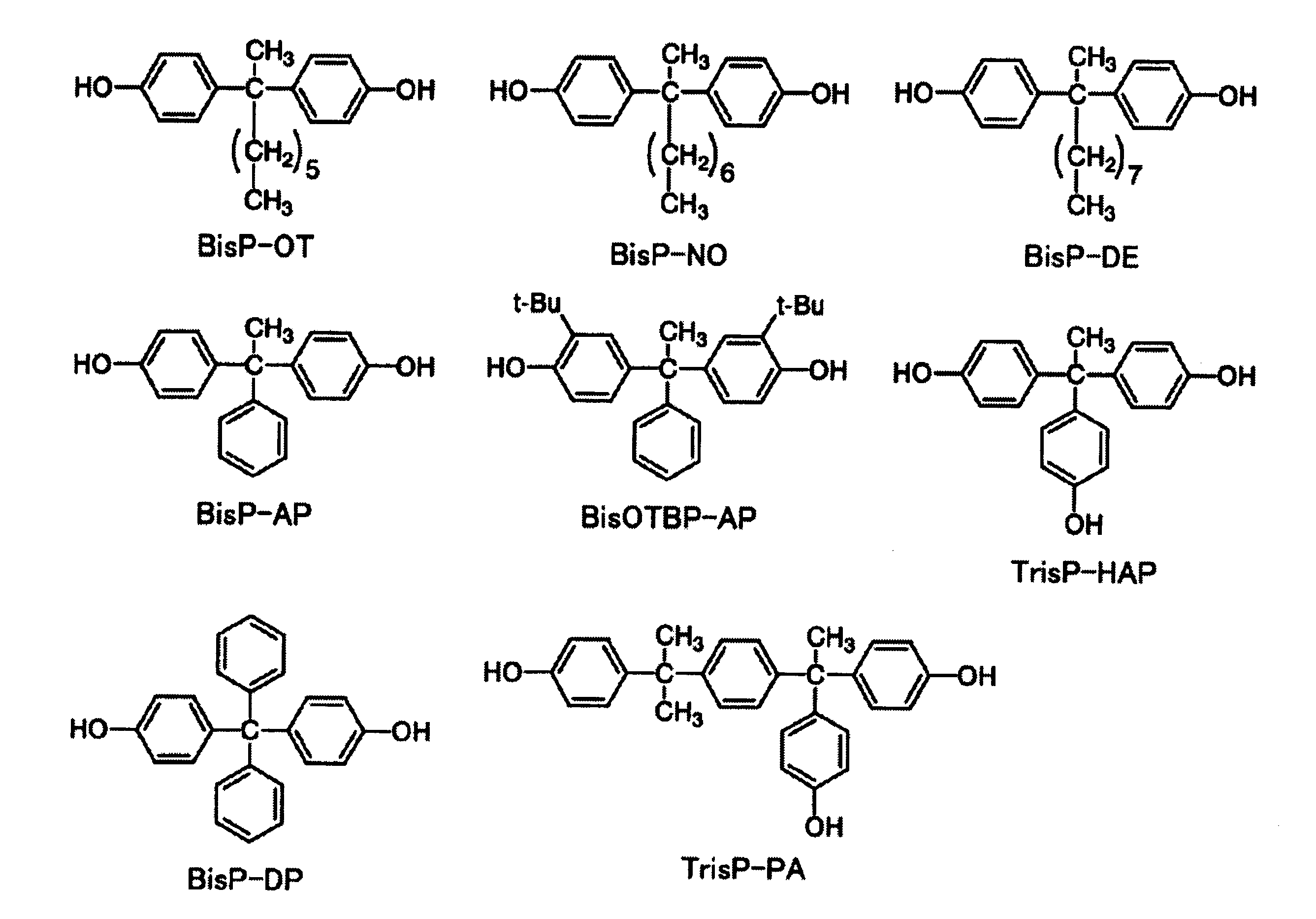
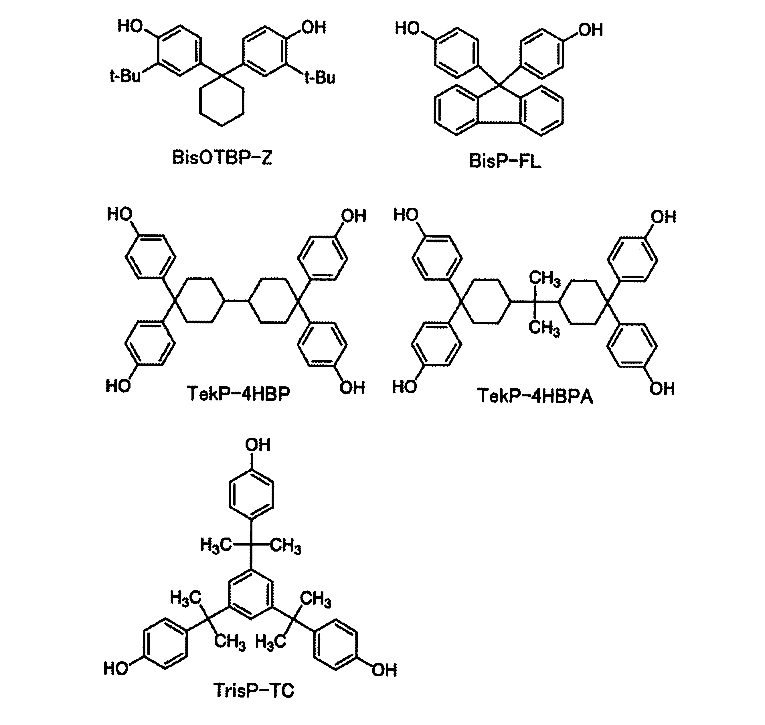
本発明に係るシロキサン組成物は、光酸発生剤を含有する。光酸発生剤は、放射線を照射した場合、分解してシラノール基の縮合を促進させる酸を放出する。ここで、放射線としては、可視光、紫外線、赤外線、X線、電子線、α線、又はγ線等が挙げられる。特に、薄膜トランジスタの製造に用いられる紫外線によって酸を発生させるものが好ましい。
R+ X- ・・・(2)
ここで、R+ は水素、炭素原子又はその他ヘテロ原子で修飾されたアルキル基、アリール基、アルケニル基、アシル基、及びアルコキシル基からなる群から選択される有機イオン、例えばジフェニルヨードニウムイオン、トリフェニルスルホニウムイオンを表す。
SbY6 -
AsY6 -
Ra pPY6-p -
Ra q BY4-q -
Ra q GaY4-q -
Ra SO3 -
(Ra SO2 )3 C-
(Ra SO2 )2 N-
Rb COO-
SCN-
(式中、Yはハロゲン原子であり、Ra は、フッ素、ニトロ基、及びシアノ基から選択される置換基で置換された、炭素数1~20のアルキル基又は炭素数6~20のアリール基であり、Rb は、水素又は炭素数1~8のアルキル基であり、pは0~6の数であり、qは0~4の数である。)

溶剤としては、例えばエチレングリコールモノメチルエーテル、エチレングリコールモノエチルエーテル、エチレングリコールモノプロピルエーテル、エチレングリコールモノブチルエーテル等のエチレングリコールモノアルキルエーテル類、ジエチレングリコールジメチルエーテル、ジエチレングリコールジエチルエーテル、ジエチレングリコールジプロピルエーテル、ジエチレングリコールジブチルエーテル等のジエチレングリコールジアルキルエーテル類、メチルセロソルブアセテート、エチルセロソルブアセテート等のエチレングリコールアルキルエーテルアセテート類、プロピレングリコールモノメチルエーテルアセテート(PGMEA)、プロピレングリコールモノエチルエーテルアセテート、プロピレングリコールモノプロピルエーテルアセテート等のプロピレングリコールアルキルエーテルアセテート類、ベンゼン、トルエン、キシレン等の芳香族炭化水素類、メチルエチルケトン、アセトン、メチルアミルケトン、メチルイソブチルケトン、シクロヘキサノン等のケトン類、エタノール、プロパノール、ブタノール、ヘキサノール、シクロヘキサノール、エチレングリコール、グリセリン等のアルコール類、3-エトキシプロピオン酸エチル、3-メトキシプロピオン酸メチル等のエステル類、γ-ブチロラクトン等の環状エステル類等が挙げられる。これらの溶剤は、夫々単独で又は2種以上を組み合わせて用いることができ、その使用量は塗布方法及び塗布後の膜厚の要求量によって決定される。
以下、本発明に係るアクティブマトリクス基板、該アクティブマトリクス基板を備える表示装置、及びアクティブマトリクス基板の製造方法について説明する。
図1は本発明の実施の形態1に係るテレビジョン受信機(以下、TV受信機という)1を示す模式的斜視図、図2は実施の形態1に係る表示パネル3を示す模式的断面図、図3は実施の形態1に係るアクティブマトリクス基板30の画素を示す模式的平面図、図4はアクティブマトリクス基板30のTFT25が設けられている部分を示す模式的断面図、図5はアクティブマトリクス基板30のゲート配線11とソース配線12とが交叉する部分を示す模式的断面図である。
表示モジュール2は、前後に縦姿勢で配置された前キャビネット4及び後キャビネット5に縦姿勢で収容されている。前キャビネット4は表示モジュール2の周縁部を覆う矩形状の枠体であり、中央に矩形の開口2aを有する。前キャビネット4は例えばプラスチック材からなる。後キャビネット5は、前側が開放された矩形のトレイ状をなし、例えばプラスチック材からなる。尚、前キャビネット4及び後キャビネット5は他の材料から構成してもよい。
該シロキサン組成物は後工程の熱履歴に対して耐熱性を有する材料であり、例えばゲート絶縁膜15の成膜工程において熱履歴を受けてもデバイス特性上問題となる物性変化を起こさない。ゲート絶縁膜15の成膜工程の熱履歴に耐えるためには、300℃以上の耐熱性を有するのが好ましい。本発明において、耐熱性は、シロキサン組成物の硬化過程及び硬化過程以後に晒される熱履歴後において、電気絶縁性、誘電率、透明膜の着色、白化、膜厚等の安定性が保持できる温度で定義される。すなわち、熱履歴を受けた後に前記物性が保持されている。
さらに、層間絶縁膜14の比誘電率は4以下であるのが好ましい。
膜べり=((i)-(ii))/(i)(%)
層間絶縁膜14は絶縁基板10を覆うように形成されている。ゲート電極11a上及び容量配線13上で、夫々の端縁部を除く部分は層間絶縁膜14により覆われず、開口部Ca,Caが形成されている。層間絶縁膜14上、ゲート電極11a上、及び容量配線13上にはゲート絶縁膜15が形成され、ゲート絶縁膜15上の、ゲート電極11a側の開口部Caに対応する部分に半導体膜16が形成されている。そして、半導体膜16を覆うようにn+ 膜17が形成され、ソース領域及びドレイン領域が形成されており、ソース領域上及びドレイン領域上にソース電極18及びドレイン電極19が形成されている。ゲート電極11a、ゲート絶縁膜15、半導体膜16、n+ 膜17、ソース電極18、及びドレイン電極19によりTFT25が構成される。
画素電極23は、開口部Caの上側の開口部Cbにおいて容量電極20に接続され、容量電極20がゲート絶縁膜15を介して容量配線13に重なることにより、補助容量が構成されている。容量電極20は、ドレイン配線27によりドレイン電極19に接続されている。
まず、ガラス基板等の絶縁基板10の基板全体に、スパッタリング法により、例えば、チタン膜(厚さ50nm程度)、アルミニウム膜(厚さ200nm程度)及びチタン膜(厚さ100nm程度)等を順に積層した金属膜を成膜し、その後、フォトマスクを用いたフォトリソグラフィ、金属膜のドライエッチング、レジストの剥離、及び洗浄を行うことにより、ゲート配線(ゲート電極11aとなる部分も形成される)11、容量配線13を形成する(図6A)。なお、金属膜は上記の三層構造に限定されず、Cu膜等であってもよい。
まず、本発明に係るシロキサン組成物をスピンコートにより、ゲート配線11、及び容量配線13を含む基板10上に塗布し、膜14aを形成する(S1、図6B)。
プリベーク後、フォトマスク26を用いて膜14aに露光する(S3、図6C)。
露光後、2.38%TMAH水溶液により現像する(S4)。これにより、開口部Ca,Ca等が、残渣等なく抜けたパターンが形成される。
最後に、例えば250℃でポストベークし、膜14aを硬化させて層間絶縁膜14を得る(S5、図6D)。
層間絶縁膜14は、上述したように、300℃以上の耐熱性を有しており、ゲート絶縁膜15の成膜工程の熱履歴を受けても物性変化を起こさない。
そして、例えばスパッタリング法によりMo等を堆積し、パターニングすることにより、ソース電極18、及びドレイン電極19を形成する(図7F)。このとき、ゲート絶縁膜15上の、容量配線13側の開口部Caに対応する部分に容量電極20を形成する(不図示)。
層間絶縁膜22上に、例えばスパッタリング法によりITO膜を形成し、パターニングすることにより画素電極23を形成する(図7H)。
そして、層間絶縁膜14の透過率は90%以上であり、該層間絶縁膜14を有するアクティブマトリクス基板30を備える表示パネル3の透過率は良好である。
本発明の実施の形態2に係る表示モジュールは、アクティブマトリクス基板34の層間絶縁膜14とゲート絶縁膜15との成膜の順序が異なること以外は、実施の形態1に係る表示モジュール2と同一の構成を有する。図9はアクティブマトリクス基板34のTFT35が設けられている部分を示す模式的断面図、図10はアクティブマトリクス基板34のゲート配線11とソース配線12とが交叉する部分を示す模式的断面図である。図9及び図10中、図4及び図5と同一部分は同一符号を付して詳細な説明を省略する。
層間絶縁膜14は、上記と同様の本発明に係るシロキサン組成物を有するSOG材料を用いてなる。
ゲート絶縁膜15は、絶縁基板10、ゲート電極11aを含むゲート配線11、及び容量配線13を覆うように形成されている。層間絶縁膜14はゲート絶縁膜15を覆うように形成されている。そして、層間絶縁膜14のゲート電極11a上、及び容量配線13上に対応する部分には、開口部Ca,Caが形成されている。層間絶縁膜14のゲート電極11a側の開口部Caには半導体膜16及びn+ 膜17がこの順に形成されている。
層間絶縁膜14の透過率は90%以上であり、表示パネル3の透過率は良好である。
本発明の実施の形態3に係る表示装置は、アクティブマトリクス基板36において、半導体膜16及びn+ 膜17を形成した後に層間絶縁膜14を形成してあること以外は、実施の形態2に係る表示装置と同一の構成を有する。図11はアクティブマトリクス基板36のTFT37が設けられている部分を示す模式的断面図である。アクティブマトリクス基板36において、ゲート配線11とソース配線12とが交叉する部分の構成は、実施の形態2に係るゲート配線11とソース配線12とが交叉する部分の構成と同一である。図11中、図9と同一部分は同一符号を付して詳細な説明を省略する。
ゲート絶縁膜15は、絶縁基板10、ゲート電極11aを含むゲート配線11、及び容量配線13を覆うように形成されている。ゲート絶縁膜15のゲート電極11a上に対応する部分には半導体膜16及びn+ 膜17がこの順に形成されている。層間絶縁膜14はゲート絶縁膜15を覆うように形成されている。層間絶縁膜14のゲート電極11a上、及び容量配線13上に対応する部分には、開口部Ca,Caが形成されている。
層間絶縁膜14の透過率は90%以上であり、表示パネル3の透過率は良好である。
本発明の実施の形態4に係る表示装置は、アクティブマトリクス基板38の層間絶縁膜22の材料が層間絶縁膜14と同様の本発明に係るシロキサン組成物を含むこと以外は、実施の形態1に係る表示モジュール2と同一の構成を有する。図12はアクティブマトリクス基板38のTFT39が設けられている部分を示す模式的断面図である。アクティブマトリクス基板38において、ゲート配線11とソース配線12とが交叉する部分の構成は、実施の形態1に係るゲート配線11とソース配線12とが交叉する部分の構成と同一である。図12中、図4と同一部分は同一符号を付して詳細な説明を省略する。
従って、本実施の形態においては、アクティブマトリクス基板38を構成する膜の材料、及び成膜の設備を共通化することができ、製造コストを低減化させることができ、材料の管理を容易にすることができる。
本発明の実施の形態5に係る表示装置は、アクティブマトリクス基板40において、層間絶縁膜14の形成パターンが異なること以外は、実施の形態2に係る表示装置と同様の構成を有する。図13はアクティブマトリクス基板40のTFT41が設けられている部分を示す模式的断面図、図14はアクティブマトリクス基板40のゲート配線11とソース配線12とが交叉する部分を示す模式的断面図である。図13及び図14中、図9及び図10と同一部分は同一符号を付して詳細な説明を省略する。
層間絶縁膜14は、上記と同様の本発明に係るシロキサン組成物を用いてなる。
上述したように、ゲート配線11のゲート電極11aが形成されている部分の上側には層間絶縁膜14は形成されていない。また、容量配線13の上側、及びゲート配線11と容量配線13との間にも層間絶縁膜14は形成されていない。
先ず、本発明のポリシロキサンの合成例を以下に示す。なお、測定にあたって、次の装置を用いた。
GPC:HLC-8220GPC(東ソー株式会社製)
スピンコーター:MS-A100(ミカサ株式会社製)
撹拌機、温度計、冷却管を備えた2Lのフラスコに、25質量%テトラメチルアンモニウムヒドロキシド(TMAH)水溶液36.5g、イソプロピルアルコール(IPA)800ml、水2.0gを仕込み、次いで滴下ロートにフェニルトリメトキシシラン39.7g、メチルトリメトキシシラン34.1g、テトラメトキシシラン7.6gの混合溶液を調整した。その混合溶液を10℃にて前記フラスコ内に滴下し、同温で3時間撹拌した後、10%HCl水溶液を加え中和した。中和液にトルエン400ml、水100mlを添加し、2層に分離させ、得られた有機層を減圧下濃縮することで溶媒を除去し、濃縮物に固形分濃度40質量%となるようにプロピレングリコールモノメチルエーテルアセテート(PGMEA)を添加調整した。
得られたポリシロキサンの分子量(ポリスチレン換算)をGPCにて測定したところ、質量平均分子量(以下「Mw」と略記することがある。)=2,200であった。また、得られた樹脂溶液をシリコンウエハにプリベーク後の膜厚が2μmになるようにスピンコーターにより塗布し、プリベーク後5%TMAH水溶液に対する溶解速度(以下「ADR」と略記することがある。)を測定したところ、490Å/秒であった。
合成例1と同様にして、25質量%TMAH水溶液54.7g、IPA800mlを仕込み、ついで滴下ロートにフェニルトリメトキシシラン39.7g、メチルトリメトキシシラン34.1g、テトラメトキシシラン7.6gの混合溶液を調整した。その混合溶液を10℃にて前記フラスコ内に滴下し、同温で3時間撹拌した後、10%HCl水溶液を加え中和した。中和液にトルエン400ml、水100mlを添加し、2層に分離させ、得られた有機層を減圧下濃縮することで溶媒を除去し、濃縮物に固形分濃度40質量%となるようにPGMEAを添加調整した。得られたポリシロキサンの分子量(ポリスチレン換算)、2.38%TMAH水溶液に対するADRを合成例1と同様にして測定したところ、Mw=1,810であり、2.38%TMAH水溶液に対するADRは、1,470Å/秒であった。
(Ia):(Ib)=(12質量%):(88質量%)の割合で混ぜたポリシロキサン、4-4’-(1-(4-(1-(4-ヒドロキシフェノール)-1-メチルエチル)フェニル)エチリデン)ビスフェノールのジアゾナフトキノン2.8モル変性体(以下「PAC」と略す)をポリシロキサンに対して6質量%、ボロン酸系の光酸発生剤「CPI-310B」(サンアプロ社製)(以下「PAG」と略す)をポリシロキサンに対して3質量%、また界面活性剤として「KF-53」(信越化学工業株式会社製)をポリシロキサンに対して0.3質量%の混合物を固形分とし、溶剤としてPGMEA94%とガンマブチロラクトン6%との混合溶媒により固形分濃度が35%になるように調整して、感光性シロキサン組成物1を得た。
PACをポリシロキサンに対し6質量%から9質量%に変更した以外、実施例1と同様に感光性シロキサン組成物2を得た。
実施例1と同様に基板に塗布し、パターンを形成し、パターンの解像性を確認したところ、5μmのコンタクトホールパターンが残渣なく抜けていることが確認された。また、実施例1と同様に光透過率を測定し、膜厚2μmあたりの波長400nmでの光透過率を求めたところ、92%であった。また、実施例1と同様に平均膜厚を求めたところ、2.17μmから2.10μmに減少し、膜べりは3.2%であった。
PAGを添加しない以外、実施例1と同様に感光性シロキサン組成物3を得た。
実施例1と同様に基板に塗布しパターンを形成し、パターンの解像性を確認したところ、20μmのコンタクトホールを形成することができなかった。現像直後は、実施例1と同様に3μmのコンタクトホールのパターンが確認できることから、230℃の加熱硬化時にパターンが熱フローして、コンタクトホールが塞がったと考えられる。また、実施例1と同様に光透過率を測定し、膜厚2μmあたりの波長400nmでの光透過率を求めたところ、97%であった。また、実施例1と同様に平均膜厚を求めたところ、2.16μmから2.09μmに減少し、膜べりは3.2%であった。
PAGを添加せず、PACをポリシロキサンに対して6質量%から12質量%に変更した以外、実施例1と同様に感光性シロキサン組成物4を得た。
実施例1と同様に基板に塗布しパターンを形成し、パターンの解像性を確認したところ、5μmのコンタクトホールパターンが抜けていることが確認された。また、実施例1と同様に光透過率を測定し、膜厚2μmあたりの波長400nmでの光透過率を求めたところ、87%であった。また、実施例1と同様に平均膜厚を求めたところ、2.17μmから2.09μmに減少し、膜べりは3.7%であった。
2 表示モジュール(表示装置)
3 表示パネル(表示装置)
30、34、36、38、40 アクティブマトリクス基板
10 絶縁基板
11 ゲート配線
11a ゲート電極
12 ソース配線
13 容量配線
14 層間絶縁膜
15 ゲート絶縁膜
16 半導体膜
17 n+ 膜
18 ソース電極
19 ドレイン電極
20 容量電極
21 パッシベーション膜
22 層間絶縁膜
23 画素電極
25、35、37、39、41 TFT
Ca、Cb 開口部
31 対向基板
32 液晶層
Claims (10)
- (I)テトラメチルアンモニウムヒドロキシド(TMAH)水溶液に対する溶解速度が異なる少なくとも2種類以上のポリシロキサン、(II)ジアゾナフトキノン誘導体、(III)光酸発生剤、及び(IV)溶剤を含有するポジ型感光性シロキサン組成物であって、
前記ポリシロキサン(I)が、
(A)下記一般式(1):
R1 nSi(OR2 )4-n
(式中、R1 は、任意のメチレンが酸素で置き換えられてもよい炭素数1~20の直鎖状、分岐状若しくは環状のアルキル基、又は炭素数6~20で任意の水素がフッ素で置き換えられてもよいアリール基を表し、R2 は、炭素数1~5のアルキル基を表し、nは0又は1を表す。)
で表されるシラン化合物を塩基性触媒の存在下で加水分解及び縮合させて得られるプリベーク後の膜が5質量%TMAH水溶液に可溶であり、その溶解速度が1000Å/秒以下であるポリシロキサン(Ia)と、
(B)前記一般式(1)で表されるシラン化合物を塩基性触媒又は酸性触媒の存在下で加水分解及び縮合させて得られるプリベーク後の膜の2.38質量%TMAH水溶液に対する溶解速度が100Å/秒以上であるポリシロキサン(Ib)と
の混合物であることを特徴とするポジ型感光性シロキサン組成物。 - 前記ポリシロキサンが、一般式(1)におけるn=0のシラン化合物を20モル%以下で反応させて得られたことを特徴とする、請求項1に記載のポジ型感光性シロキサン組成物。
- 前記ジアゾナフトキノン誘導体、及び前記光酸発生剤の量が、前記ポリシロキサン(I)100質量部に対して、夫々3質量部以上10質量部以下、及び0.01質量部以上10質量部以下であることを特徴とする請求項1又は2に記載のポジ型感光性シロキサン組成物。
- 基板上に、複数のソース配線と複数のゲート配線とを立体的に交叉するように形成し、前記ソース配線と前記ゲート配線とが交叉する部分の近傍に薄膜トランジスタを形成し、該薄膜トランジスタを介して対応するソース配線に電気的に接続される画素電極を形成してあり、少なくとも前記ソース配線と前記ゲート配線との間に、請求項1から3までのいずれか1項のポジ型感光性シロキサン組成物の硬化物からなる層間絶縁膜が介在することを特徴とするアクティブマトリクス基板。
- 前記層間絶縁膜が、
300℃以上の耐熱性を有し、
光透過率が90%以上であり、
300℃における膜厚減少量が5%以下であり、
比誘電率が4以下であることを特徴とする請求項1に記載のアクティブマトリクス基板。 - 前記層間絶縁膜が、前記ソース配線と前記ゲート配線とが交叉する部分に形成してあることを特徴とする請求項4又は5に記載のアクティブマトリクス基板。
- 前記薄膜トランジスタの上側に、前記硬化物からなる層間絶縁膜をさらに有することを特徴とする請求項4から6までのいずれか1項に記載のアクティブマトリクス基板。
- 請求項4から7までのいずれか1項に記載のアクティブマトリクス基板と、
該アクティブマトリクス基板上に配置された表示媒体層と、
前記アクティブマトリクス基板に前記表示媒体層を介して対向する対向基板と
を備えることを特徴とする表示装置。 - 基板上に、複数のソース配線と複数のゲート配線とを立体的に交叉するように形成し、前記ソース配線と前記ゲート配線とが交叉する部分の近傍に薄膜トランジスタを形成し、該薄膜トランジスタを介して対応するソース配線に電気的に接続される画素電極を形成する工程を有し、少なくとも前記ソース配線と前記ゲート配線との間に、請求項1から3までのいずれか1項のポジ型感光性シロキサン組成物の硬化物からなる層間絶縁膜を形成する層間絶縁膜形成工程を有するアクティブマトリクス基板の製造方法であって、
前記層間絶縁膜形成工程が、
前記ポジ型感光性シロキサン組成物を用いて膜を形成する膜形成工程と、
形成した膜をプリベークする工程と、
プリベークした膜を露光する工程と、
露光した膜を現像する工程と、
現像した膜を焼成する工程と
を有することを特徴とするアクティブマトリクス基板の製造方法。 - 前記膜形成工程は、前記ソース配線と前記ゲート配線とが交叉する部分に膜を形成することを特徴とする請求項9に記載のアクティブマトリクス基板の製造方法。
Priority Applications (6)
| Application Number | Priority Date | Filing Date | Title |
|---|---|---|---|
| SG11201706317QA SG11201706317QA (en) | 2015-02-04 | 2016-02-03 | Positive photosensitive siloxane composition, active matrix substrate, display device, and method for producing active matrix substrate |
| JP2016573406A JP6487947B2 (ja) | 2015-02-04 | 2016-02-03 | ポジ型感光性シロキサン組成物、アクティブマトリクス基板、表示装置、及びアクティブマトリクス基板の製造方法 |
| EP16746667.1A EP3255494A4 (en) | 2015-02-04 | 2016-02-03 | Positive photosensitive siloxane composition, active matrix substrate, display device, and method for producing active matrix substrate |
| US15/546,596 US10620538B2 (en) | 2015-02-04 | 2016-02-03 | Positive type photosensitive siloxane composition, active matrix substrate, display apparatus, and method of manufacturing active matrix substrate |
| KR1020177024753A KR102615352B1 (ko) | 2015-02-04 | 2016-02-03 | 포지티브형 감광성 실록산 조성물, 액티브 매트릭스 기판, 표시 장치, 및 액티브 매트릭스 기판의 제조 방법 |
| CN201680007695.3A CN107209456A (zh) | 2015-02-04 | 2016-02-03 | 正型感光性硅氧烷组合物、有源矩阵基板、显示装置以及有源矩阵基板的制造方法 |
Applications Claiming Priority (2)
| Application Number | Priority Date | Filing Date | Title |
|---|---|---|---|
| JP2015-020399 | 2015-02-04 | ||
| JP2015020399 | 2015-02-04 |
Publications (1)
| Publication Number | Publication Date |
|---|---|
| WO2016125836A1 true WO2016125836A1 (ja) | 2016-08-11 |
Family
ID=56564175
Family Applications (1)
| Application Number | Title | Priority Date | Filing Date |
|---|---|---|---|
| PCT/JP2016/053261 WO2016125836A1 (ja) | 2015-02-04 | 2016-02-03 | ポジ型感光性シロキサン組成物、アクティブマトリクス基板、表示装置、及びアクティブマトリクス基板の製造方法 |
Country Status (8)
| Country | Link |
|---|---|
| US (1) | US10620538B2 (ja) |
| EP (1) | EP3255494A4 (ja) |
| JP (1) | JP6487947B2 (ja) |
| KR (1) | KR102615352B1 (ja) |
| CN (1) | CN107209456A (ja) |
| SG (1) | SG11201706317QA (ja) |
| TW (1) | TWI698713B (ja) |
| WO (1) | WO2016125836A1 (ja) |
Cited By (1)
| Publication number | Priority date | Publication date | Assignee | Title |
|---|---|---|---|---|
| KR20200060466A (ko) * | 2017-09-27 | 2020-05-29 | 메르크 파텐트 게엠베하 | 포지티브형 감광성 실록산 조성물 및 이를 사용하는 경화 막 |
Families Citing this family (5)
| Publication number | Priority date | Publication date | Assignee | Title |
|---|---|---|---|---|
| US10916661B2 (en) * | 2016-11-28 | 2021-02-09 | Merck Patent Gmbh | Thin film transistor substrate provided with protective film and method for producing same |
| US10840269B2 (en) * | 2017-03-29 | 2020-11-17 | Sharp Kabushiki Kaisha | Semiconductor device and method of manufacturing semiconductor device |
| WO2020187685A1 (en) * | 2019-03-15 | 2020-09-24 | Merck Patent Gmbh | Positive type photosensitive polysiloxane composition |
| JP6639724B1 (ja) * | 2019-03-15 | 2020-02-05 | メルク、パテント、ゲゼルシャフト、ミット、ベシュレンクテル、ハフツングMerck Patent GmbH | ポジ型感光性ポリシロキサン組成物 |
| US11467494B2 (en) | 2019-03-15 | 2022-10-11 | Merck Patent Gmbh | Positive type photosensitive polysiloxane composition |
Citations (5)
| Publication number | Priority date | Publication date | Assignee | Title |
|---|---|---|---|---|
| WO2011104791A1 (ja) * | 2010-02-25 | 2011-09-01 | シャープ株式会社 | 薄膜トランジスタ基板及びその製造方法、表示装置 |
| WO2012026400A1 (ja) * | 2010-08-24 | 2012-03-01 | Azエレクトロニックマテリアルズ株式会社 | ポジ型感光性シロキサン組成物 |
| WO2012161025A1 (ja) * | 2011-05-20 | 2012-11-29 | AzエレクトロニックマテリアルズIp株式会社 | ポジ型感光性シロキサン組成物 |
| JP2014106250A (ja) * | 2012-11-22 | 2014-06-09 | Az Electronic Materials Mfg Co Ltd | ポジ型感光性シロキサン組成物 |
| WO2014163118A1 (ja) * | 2013-04-05 | 2014-10-09 | 堺ディスプレイプロダクト株式会社 | アクティブマトリクス回路、アクティブマトリクス回路の製造方法、及び画像表示装置 |
Family Cites Families (17)
| Publication number | Priority date | Publication date | Assignee | Title |
|---|---|---|---|---|
| JPH01241873A (ja) * | 1988-03-24 | 1989-09-26 | Seiko Epson Corp | ジョセフソン電界効果トランジスタ及びその製造方法 |
| JP3229419B2 (ja) | 1993-02-10 | 2001-11-19 | ダウ・コ−ニング・コ−ポレ−ション | 酸化ケイ素膜の形成方法 |
| US5380555A (en) | 1993-02-09 | 1995-01-10 | Dow Corning Toray Silicone Co., Ltd. | Methods for the formation of a silicon oxide film |
| JP2001098224A (ja) | 1999-09-28 | 2001-04-10 | Hitachi Chem Co Ltd | シリカ系被膜、シリカ系被膜の形成方法及びシリカ系被膜を有する電子部品 |
| US6984476B2 (en) * | 2002-04-15 | 2006-01-10 | Sharp Kabushiki Kaisha | Radiation-sensitive resin composition, forming process for forming patterned insulation film, active matrix board and flat-panel display device equipped with the same, and process for producing flat-panel display device |
| US8158981B2 (en) * | 2006-09-25 | 2012-04-17 | Hitachi Chemical Company, Ltd. | Radiation-sensitive composition, method of forming silica-based coating film, silica-based coating film, apparatus and member having silica-based coating film and photosensitizing agent for insulating film |
| WO2009028360A1 (ja) * | 2007-08-24 | 2009-03-05 | Toray Industries, Inc. | 感光性組成物、それから形成された硬化膜、および硬化膜を有する素子 |
| JP2009186677A (ja) * | 2008-02-05 | 2009-08-20 | Hitachi Chem Co Ltd | 感光性樹脂組成物、シリカ系被膜の形成方法、及びシリカ系被膜を備える装置及び部材 |
| JP4916461B2 (ja) | 2008-02-18 | 2012-04-11 | シャープ株式会社 | アクティブマトリクス基板およびそれを備えた表示装置 |
| JP2010117696A (ja) * | 2008-10-17 | 2010-05-27 | Hitachi Chem Co Ltd | 感光性樹脂組成物、シリカ系被膜の形成方法、及びシリカ系被膜を備える装置及び部材 |
| CN102696112A (zh) * | 2009-12-21 | 2012-09-26 | 夏普株式会社 | 有源矩阵基板和具有其的显示面板、以及有源矩阵基板的制造方法 |
| JP2011181462A (ja) * | 2010-03-03 | 2011-09-15 | Hitachi Displays Ltd | 表示パネルの製造方法 |
| JP5698070B2 (ja) * | 2011-05-11 | 2015-04-08 | 株式会社Adeka | ポジ型感光性組成物及びその硬化物 |
| JP5726632B2 (ja) * | 2011-05-19 | 2015-06-03 | メルクパフォーマンスマテリアルズIp合同会社 | 感光性シロキサン樹脂組成物 |
| JP6086739B2 (ja) * | 2013-01-21 | 2017-03-01 | 東京応化工業株式会社 | 絶縁膜形成用組成物、絶縁膜の製造方法、及び絶縁膜 |
| JP6065665B2 (ja) * | 2013-03-11 | 2017-01-25 | Jsr株式会社 | 感放射線性樹脂組成物、硬化膜、発光表示素子および発光層の形成方法 |
| KR20150068899A (ko) * | 2013-12-12 | 2015-06-22 | 제이엔씨 주식회사 | 포지티브형 감광성 조성물 |
-
2016
- 2016-02-03 CN CN201680007695.3A patent/CN107209456A/zh active Pending
- 2016-02-03 KR KR1020177024753A patent/KR102615352B1/ko active IP Right Grant
- 2016-02-03 JP JP2016573406A patent/JP6487947B2/ja active Active
- 2016-02-03 SG SG11201706317QA patent/SG11201706317QA/en unknown
- 2016-02-03 WO PCT/JP2016/053261 patent/WO2016125836A1/ja active Application Filing
- 2016-02-03 EP EP16746667.1A patent/EP3255494A4/en active Pending
- 2016-02-03 US US15/546,596 patent/US10620538B2/en active Active
- 2016-02-04 TW TW105103763A patent/TWI698713B/zh active
Patent Citations (5)
| Publication number | Priority date | Publication date | Assignee | Title |
|---|---|---|---|---|
| WO2011104791A1 (ja) * | 2010-02-25 | 2011-09-01 | シャープ株式会社 | 薄膜トランジスタ基板及びその製造方法、表示装置 |
| WO2012026400A1 (ja) * | 2010-08-24 | 2012-03-01 | Azエレクトロニックマテリアルズ株式会社 | ポジ型感光性シロキサン組成物 |
| WO2012161025A1 (ja) * | 2011-05-20 | 2012-11-29 | AzエレクトロニックマテリアルズIp株式会社 | ポジ型感光性シロキサン組成物 |
| JP2014106250A (ja) * | 2012-11-22 | 2014-06-09 | Az Electronic Materials Mfg Co Ltd | ポジ型感光性シロキサン組成物 |
| WO2014163118A1 (ja) * | 2013-04-05 | 2014-10-09 | 堺ディスプレイプロダクト株式会社 | アクティブマトリクス回路、アクティブマトリクス回路の製造方法、及び画像表示装置 |
Non-Patent Citations (1)
| Title |
|---|
| See also references of EP3255494A4 * |
Cited By (3)
| Publication number | Priority date | Publication date | Assignee | Title |
|---|---|---|---|---|
| KR20200060466A (ko) * | 2017-09-27 | 2020-05-29 | 메르크 파텐트 게엠베하 | 포지티브형 감광성 실록산 조성물 및 이를 사용하는 경화 막 |
| US20200225583A1 (en) * | 2017-09-27 | 2020-07-16 | Merck Patent Gmbh | Positive type photosensitive siloxane composition and cured film using the same |
| KR102614196B1 (ko) * | 2017-09-27 | 2023-12-19 | 메르크 파텐트 게엠베하 | 포지티브형 감광성 실록산 조성물 및 이를 사용하는 경화 막 |
Also Published As
| Publication number | Publication date |
|---|---|
| TWI698713B (zh) | 2020-07-11 |
| KR102615352B1 (ko) | 2023-12-20 |
| US20180017869A1 (en) | 2018-01-18 |
| KR20170110138A (ko) | 2017-10-10 |
| US10620538B2 (en) | 2020-04-14 |
| CN107209456A (zh) | 2017-09-26 |
| TW201629631A (zh) | 2016-08-16 |
| EP3255494A1 (en) | 2017-12-13 |
| JPWO2016125836A1 (ja) | 2018-01-18 |
| JP6487947B2 (ja) | 2019-03-20 |
| EP3255494A4 (en) | 2018-10-10 |
| SG11201706317QA (en) | 2017-09-28 |
Similar Documents
| Publication | Publication Date | Title |
|---|---|---|
| JP6487947B2 (ja) | ポジ型感光性シロキサン組成物、アクティブマトリクス基板、表示装置、及びアクティブマトリクス基板の製造方法 | |
| JP6267282B2 (ja) | ポジ型感光性シロキサン組成物 | |
| JP5707407B2 (ja) | ポジ型感光性シロキサン組成物 | |
| US8158981B2 (en) | Radiation-sensitive composition, method of forming silica-based coating film, silica-based coating film, apparatus and member having silica-based coating film and photosensitizing agent for insulating film | |
| JP6013150B2 (ja) | ポジ型感光性シロキサン組成物の製造方法 | |
| US8546061B2 (en) | Photo-curing polysiloxane composition and protective film formed from the same | |
| US20120237873A1 (en) | Positive photosensitive resin composition, cured film formed from the same, and device having cured film | |
| JP6487126B2 (ja) | ポジ型感光性シロキサン組成物 | |
| US8349461B2 (en) | Photo-curing polysiloxane composition and protective film formed from the same | |
| TWI518460B (zh) | Photosensitive polysiloxane compositions and their use | |
| US20130280541A1 (en) | Photo-curing polysiloxane composition and application thereof | |
| US20150293449A1 (en) | Photosensitive polysiloxane composition and uses thereof | |
| JP2012155226A (ja) | ポジ型感放射線性組成物、硬化膜、硬化膜の形成方法、表示素子、及び硬化膜形成用のポリシロキサン | |
| US20140242504A1 (en) | Positive photosensitive resin composition and method for forming patterns by using the same | |
| CN107561863B (zh) | 正型感光性树脂组成物及其应用 | |
| TWI541595B (zh) | Photosensitive polysiloxane compositions and their use | |
| US20220267639A1 (en) | Gate insulating film forming composition | |
| CN107179652B (zh) | 正型感光性聚硅氧烷组成物及其应用 | |
| TWI617883B (zh) | 正型感光性樹脂組成物及其應用 | |
| TW202136421A (zh) | 樹脂組成物、硬化膜、微透鏡的製造方法、固體攝像元件、微透鏡、觸控面板 |
Legal Events
| Date | Code | Title | Description |
|---|---|---|---|
| 121 | Ep: the epo has been informed by wipo that ep was designated in this application |
Ref document number: 16746667 Country of ref document: EP Kind code of ref document: A1 |
|
| WWE | Wipo information: entry into national phase |
Ref document number: 15546596 Country of ref document: US |
|
| ENP | Entry into the national phase |
Ref document number: 2016573406 Country of ref document: JP Kind code of ref document: A |
|
| WWE | Wipo information: entry into national phase |
Ref document number: 11201706317Q Country of ref document: SG |
|
| NENP | Non-entry into the national phase |
Ref country code: DE |
|
| REEP | Request for entry into the european phase |
Ref document number: 2016746667 Country of ref document: EP |
|
| ENP | Entry into the national phase |
Ref document number: 20177024753 Country of ref document: KR Kind code of ref document: A |