WO2016125492A1 - Iii族窒化物半導体発光素子およびその製造方法 - Google Patents
Iii族窒化物半導体発光素子およびその製造方法 Download PDFInfo
- Publication number
- WO2016125492A1 WO2016125492A1 PCT/JP2016/000566 JP2016000566W WO2016125492A1 WO 2016125492 A1 WO2016125492 A1 WO 2016125492A1 JP 2016000566 W JP2016000566 W JP 2016000566W WO 2016125492 A1 WO2016125492 A1 WO 2016125492A1
- Authority
- WO
- WIPO (PCT)
- Prior art keywords
- layer
- group iii
- iii nitride
- nitride semiconductor
- type
- Prior art date
- Legal status (The legal status is an assumption and is not a legal conclusion. Google has not performed a legal analysis and makes no representation as to the accuracy of the status listed.)
- Ceased
Links
Images


Classifications
-
- H—ELECTRICITY
- H10—SEMICONDUCTOR DEVICES; ELECTRIC SOLID-STATE DEVICES NOT OTHERWISE PROVIDED FOR
- H10H—INORGANIC LIGHT-EMITTING SEMICONDUCTOR DEVICES HAVING POTENTIAL BARRIERS
- H10H20/00—Individual inorganic light-emitting semiconductor devices having potential barriers, e.g. light-emitting diodes [LED]
- H10H20/80—Constructional details
- H10H20/81—Bodies
- H10H20/816—Bodies having carrier transport control structures, e.g. highly-doped semiconductor layers or current-blocking structures
- H10H20/8162—Current-blocking structures
-
- H—ELECTRICITY
- H10—SEMICONDUCTOR DEVICES; ELECTRIC SOLID-STATE DEVICES NOT OTHERWISE PROVIDED FOR
- H10H—INORGANIC LIGHT-EMITTING SEMICONDUCTOR DEVICES HAVING POTENTIAL BARRIERS
- H10H20/00—Individual inorganic light-emitting semiconductor devices having potential barriers, e.g. light-emitting diodes [LED]
- H10H20/01—Manufacture or treatment
- H10H20/011—Manufacture or treatment of bodies, e.g. forming semiconductor layers
- H10H20/013—Manufacture or treatment of bodies, e.g. forming semiconductor layers having light-emitting regions comprising only Group III-V materials
- H10H20/0133—Manufacture or treatment of bodies, e.g. forming semiconductor layers having light-emitting regions comprising only Group III-V materials with a substrate not being Group III-V materials
- H10H20/01335—Manufacture or treatment of bodies, e.g. forming semiconductor layers having light-emitting regions comprising only Group III-V materials with a substrate not being Group III-V materials the light-emitting regions comprising nitride materials
-
- H—ELECTRICITY
- H10—SEMICONDUCTOR DEVICES; ELECTRIC SOLID-STATE DEVICES NOT OTHERWISE PROVIDED FOR
- H10H—INORGANIC LIGHT-EMITTING SEMICONDUCTOR DEVICES HAVING POTENTIAL BARRIERS
- H10H20/00—Individual inorganic light-emitting semiconductor devices having potential barriers, e.g. light-emitting diodes [LED]
- H10H20/80—Constructional details
- H10H20/81—Bodies
- H10H20/811—Bodies having quantum effect structures or superlattices, e.g. tunnel junctions
- H10H20/812—Bodies having quantum effect structures or superlattices, e.g. tunnel junctions within the light-emitting regions, e.g. having quantum confinement structures
-
- H—ELECTRICITY
- H10—SEMICONDUCTOR DEVICES; ELECTRIC SOLID-STATE DEVICES NOT OTHERWISE PROVIDED FOR
- H10H—INORGANIC LIGHT-EMITTING SEMICONDUCTOR DEVICES HAVING POTENTIAL BARRIERS
- H10H20/00—Individual inorganic light-emitting semiconductor devices having potential barriers, e.g. light-emitting diodes [LED]
- H10H20/80—Constructional details
- H10H20/81—Bodies
- H10H20/822—Materials of the light-emitting regions
- H10H20/824—Materials of the light-emitting regions comprising only Group III-V materials, e.g. GaP
- H10H20/825—Materials of the light-emitting regions comprising only Group III-V materials, e.g. GaP containing nitrogen, e.g. GaN
-
- H—ELECTRICITY
- H10—SEMICONDUCTOR DEVICES; ELECTRIC SOLID-STATE DEVICES NOT OTHERWISE PROVIDED FOR
- H10H—INORGANIC LIGHT-EMITTING SEMICONDUCTOR DEVICES HAVING POTENTIAL BARRIERS
- H10H20/00—Individual inorganic light-emitting semiconductor devices having potential barriers, e.g. light-emitting diodes [LED]
- H10H20/80—Constructional details
- H10H20/81—Bodies
- H10H20/822—Materials of the light-emitting regions
- H10H20/824—Materials of the light-emitting regions comprising only Group III-V materials, e.g. GaP
- H10H20/825—Materials of the light-emitting regions comprising only Group III-V materials, e.g. GaP containing nitrogen, e.g. GaN
- H10H20/8252—Materials of the light-emitting regions comprising only Group III-V materials, e.g. GaP containing nitrogen, e.g. GaN characterised by the dopants
Definitions
- the present invention relates to a group III nitride semiconductor light emitting device and a method for manufacturing the same, and more particularly to a group III nitride semiconductor light emitting device having an excellent device lifetime and a method for manufacturing the same.
- group III nitride semiconductor composed of a compound of N, Al, Ga, In and the like has been used as a material for an ultraviolet light emitting element.
- group III nitride semiconductors made of AlGaN having a high Al composition are used for ultraviolet light emitting devices and deep ultraviolet light emitting devices (DUV-LEDs) having an emission wavelength of 300 nm or less.
- Examples of characteristics required for a group III nitride semiconductor light emitting device include high external quantum efficiency characteristics and low resistance characteristics.
- the applicant of the present application is to increase the light emission efficiency by forming a layer serving as an electron energy barrier called an electron block layer between the light emitting layer having a quantum well structure and the p-type cladding layer. Proposed earlier.
- the electron blocking layer serves as a barrier against the quantum well layer of the light emitting layer, and can prevent the electrons from flowing excessively, thereby improving the carrier injection efficiency.
- Patent Document 2 in a semiconductor light emitting device using a nitride-based compound semiconductor, the p-type cladding layer is locally higher than the entire p-type cladding layer on the boundary side with the p-side light guide layer.
- a semiconductor light emitting device provided with a highly doped layer doped with concentration is disclosed.
- the crystallinity of the p-type cladding layer is deteriorated by providing a high-concentration doping layer that is locally highly doped compared to the entire p-type cladding layer in a part of the p-type cladding layer. It is possible to increase the hole concentration (hole concentration), thereby reducing the series resistance and the threshold current density.
- JP 2010-161311 A Japanese Patent Laid-Open No. 2000-153103
- the external quantum efficiency characteristics and resistance characteristics of the group III nitride semiconductor light emitting device can be improved by the techniques described in Patent Document 1 and Patent Document 2.
- improvement of the element lifetime characteristics of the group III nitride semiconductor light emitting element is desired, and there is room for improvement in terms of lifetime.
- an object of the present invention is to provide a group III nitride semiconductor light-emitting device having a device lifetime superior to that of the prior art and a method for manufacturing the same.
- Mg is generally used as a p-type dopant to be doped on the p-type semiconductor layer side of the group III nitride semiconductor light emitting device.
- the present inventors thought that the diffusion of Mg doped on the p-type semiconductor layer side into the light emitting layer may affect the life characteristics of the group III nitride semiconductor light emitting device.
- the gist of the present invention is as follows. (1) In a group III nitride semiconductor light-emitting device having an n-type semiconductor layer, a light-emitting layer containing at least Al, an electron block layer, and a p-type semiconductor layer in this order, the light-emitting layer includes a well layer and a barrier layer The electron blocking layer is adjacent to the light emitting layer and is made of a layer having a larger Al composition than the barrier layer and the p-type semiconductor layer, and the electron blocking layer is A group III nitride semiconductor light-emitting device comprising a Si-containing impurity-doped region layer.
- the electron blocking layer further includes a p-type impurity doped region layer on the p-type semiconductor layer side of the Si-containing impurity doped region layer.
- the p-type semiconductor layer includes a p-type cladding layer having an Al composition smaller than that of the electron block layer and larger than that of the p-type contact layer, the electron block layer, the p-type contact layer, The group III nitride semiconductor light-emitting device according to any one of (6), further having a gap between them.
- the barrier layer is Al b Ga 1-b N (0.4 ⁇ b ⁇ 0.95), and the electron blocking layer is Al z Ga 1-z N (b ⁇ z ⁇ 1).
- the group III nitride semiconductor light-emitting device according to any one of (1) to (9).
- a group III nitride semiconductor light-emitting device having an n-type semiconductor layer, a light-emitting layer containing at least Al, an electron block layer, and a p-type semiconductor layer in this order, the light-emitting layer includes a well layer and a barrier layer
- the electron blocking layer is adjacent to the light emitting layer and is made of a layer having a larger Al composition than the barrier layer and the p-type semiconductor layer, and the electron blocking layer is A group III nitride semiconductor light-emitting device comprising a Si-containing impurity-doped region layer, wherein the electron blocking layer further includes a p-type impurity-doped region layer closer to the light-emitting layer than the Si-containing impurity-doped region layer .
- the barrier layer is Al b Ga 1-b N (0.4 ⁇ b ⁇ 0.95), and the electron blocking layer is Al z Ga 1-z N (b ⁇ z ⁇ 1).
- the group III nitride semiconductor light-emitting device according to any one of (15) to (19), wherein the light emitted from the light-emitting layer is deep ultraviolet light having a center wavelength of 300 nm or less.
- the group III nitride semiconductor light emitting device since the Si-containing impurity doped region layer is provided in the electron blocking layer, the group III nitride semiconductor light emitting device having a longer device lifetime than the conventional one. An element and a manufacturing method thereof can be provided.
- FIG. 1 is a schematic cross-sectional view illustrating a group III nitride semiconductor light emitting device according to a first embodiment of the present invention.
- (A) to (D) are schematic cross-sectional views showing a light emitting layer, an electron blocking layer, and a p-type semiconductor layer in a group III nitride semiconductor light emitting device according to a preferred embodiment of the present invention. It is a schematic cross section explaining a group III nitride semiconductor light emitting device according to a second embodiment of the present invention.
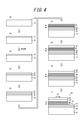
- 3 is a flowchart illustrating a method for manufacturing a group III semiconductor light emitting device according to a preferred embodiment of the present invention.
- a group III nitride semiconductor light emitting device 100 includes an n-type semiconductor layer 30, a light emitting layer 40 containing at least Al, an electron blocking layer 50, and a p-type semiconductor layer. 60 in this order.
- the light emitting layer 40 has a quantum well structure formed by stacking a well layer 41 and a barrier layer 42, and the electron block layer 50 is adjacent to the light emitting layer 40 and is more than the barrier layer 42 and the p-type semiconductor layer 60.
- the electron blocking layer 50 is composed of a layer having a large Al composition, and includes an Si-containing impurity doped region layer 50a.
- the n-type semiconductor layer 30 of the group III nitride semiconductor light emitting device 100 can be provided on an AlN template substrate in which an AlN layer 20 is provided on the surface of the substrate 10. Further, in the group III nitride semiconductor light emitting device 100, a part of the light emitting layer 40, the electron blocking layer 50 and the p type semiconductor layer 60 is removed by etching or the like, and the n type formed on the exposed n type semiconductor layer 30. An electrode 70 and a p-type electrode 80 formed on the p-type contact layer 62 may be provided.
- the group III nitride semiconductor light emitting device 100 is characterized in that the n-type semiconductor layer 30, the light emitting layer 40, the electron blocking layer 50, and the p-type semiconductor layer 60 are characterized by the electron blocking layer. 50 is a particularly characteristic configuration.
- the sapphire substrate 10, the AlN layer 20, the n-type electrode 70, and the p-type electrode 80 can have a general configuration, and the specific configuration is not limited at all.
- Each semiconductor layer in group III nitride semiconductor light emitting device 100 is made of, for example, an AlGaN material, and may contain In in an amount of 5% or less with respect to Al and Ga as group III elements.
- n-type semiconductor layer 30, the light emitting layer 40, the electron block layer 50, and the p-type semiconductor layer 60 that are the features of the present invention will be described first.
- the n-type semiconductor layer 30 is a group III nitride semiconductor layer containing at least Al, and a general n-type semiconductor layer can be used as long as the layer forms a pn junction of the group III nitride semiconductor.
- the n-type semiconductor layer 30 is made of, for example, an AlGaN material, and may contain In in an amount of 5% or less with respect to Al and Ga as group III elements.
- the n-type semiconductor layer 30 is doped with an n-type dopant (impurity), and examples of the n-type dopant include Si, Ge, Sn, S, O, Ti, and Zr.
- the dopant concentration is not particularly limited as long as it is a dopant concentration capable of functioning as n-type, and can be, for example, 1.0 ⁇ 10 18 atoms / cm 3 to 1.0 ⁇ 10 20 atoms / cm 3 .
- the Al content of the n-type semiconductor layer 30 is not particularly limited and can be in a general range.
- the n-type semiconductor layer 30 can also be composed of a single layer or a plurality of layers.
- the light emitting layer 40 is provided on the n-type semiconductor layer 30.
- the light emitting layer 40 contains at least Al, and can be formed of, for example, an Al a Ga 1-a N material (0 ⁇ a ⁇ 1).
- the composition of Al is appropriately set so as to emit light of a desired wavelength, but when the Al composition a is 0.35 or more (that is, 0.35 ⁇ a ⁇ 1),
- the center wavelength of the emitted light is 300 nm or less, and the finally produced group III nitride semiconductor light emitting device 100 is a DUV-LED.
- the light emitting layer 40 can be composed of a multiple quantum well (MQW) in which a well layer 41 and a barrier layer 42 made of AlGaN having different Al compositions are repeatedly formed.
- the Al composition of the well layer 41 is, for example, 0.3 to 0.8.
- the Al composition b of the barrier layer 42 is larger than the Al composition of the well layer 41, for example, 0.40 to 0.95. Further, the number of repetitions of the well layer 41 and the barrier layer 42 is, for example, 1 to 10 times.
- the n-type semiconductor layer 30 side and the electron blocking layer 50 side (that is, the first and last) of the light emitting layer 40 are barrier layers, and if the number of repetitions of the well layer 41 and the barrier layer 42 is n, in this case It shall be described as “n.5 sets of well layers and barrier layers”. Furthermore, the thickness of the well layer 41 can be 0.5 nm to 5 nm, and the thickness of the barrier layer 42 can be 3 nm to 30 nm.
- the electron blocking layer 50 is provided adjacent to the light emitting layer 40 and is made of a layer larger than the Al composition b of the barrier layer 42 and the Al composition of the p-type semiconductor layer 60.
- the electron blocking layer 50 is provided between the light emitting layer and the p-type cladding layer to block electrons and inject electrons into the light emitting layer 40 (well layer 41 in the case of MQW).
- it is used as a layer for increasing the electron injection efficiency.
- the Al composition of the light emitting layer 40 is high, the hole concentration of the p-type semiconductor layer 60 is low, so that it is difficult to inject holes into the light emitting layer 40 and some electrons flow to the p-type semiconductor layer 60 side.
- the “electron block layer” Al composition z means a layer having a larger band gap than the Al composition b of the barrier layer 42 constituting the light emitting layer 40.
- the “cladding layer” has an Al composition that is smaller than the Al composition of the electron blocking layer by more than 0.1 and larger than the p-type contact layer by more than 0.1.
- the p-type semiconductor layer 60 may or may not have the p-type cladding layer 61.
- the Al composition y of the p-type cladding layer 61 is the Al composition z of the electron block layer 50 and the Al composition of the p-type contact layer 62.
- the composition x is used, x + 0.1 ⁇ y ⁇ z ⁇ 0.1. Since p-type AlGaN used at a center wavelength of 300 nm or less has a smaller Al current as the Al composition increases, the Al composition conventionally used as the cladding layer is often less than or equal to the Al composition of the barrier layer. For this reason, the electron block layer in the present invention and the clad layer in the prior art are distinguished on the basis of the Al composition of the barrier layer.
- the electron block layer 50 can be formed of, for example, an Al z Ga 1-z N material (b ⁇ z ⁇ 1). Although depending on the Al composition of the barrier layer 42, for example, the Al composition of the electron block layer 50 is preferably 0.5 or more and 1.0 or less (that is, b ⁇ z ⁇ 1 and 0.5 ⁇ z). . Thereby, the injection efficiency of electrons into the well layer 41 can be increased.
- the total thickness of the electron blocking layer 50 is preferably 6 nm to 60 nm, for example. This is because, even if the thickness of the electron blocking layer 51 is less than 6 nm or exceeds 60 nm, the output is significantly reduced.
- the thickness of the electron blocking layer 50 is preferably thicker than the thickness of the barrier layer 42.
- the electron blocking layer may be doped with a p-type dopant in addition to Si.
- examples of the p-type dopant include Mg, Zn, Ca, Be, and Mn. it can.
- the average dopant concentration of the entire p-type semiconductor layer 60 is not particularly limited as long as it is a dopant concentration capable of functioning as a p-type. For example, 1.0 ⁇ 10 18 atoms / cm 3 to 5.0 ⁇ 10 21 atoms / cm 3 can be used.
- the p-type semiconductor layer 60 has at least a p-type contact layer 62.
- the p-type contact layer 62 may be a p-type Al x Ga 1-x N material having an Al composition x of 0 ⁇ x ⁇ 0.1.
- the p-type contact layer 62 is a layer for reducing the contact resistance between the p-type electrode 80 and the electron block layer 50 formed thereon, and the p-type electrode formed on the p-type contact layer 62.
- the contact resistance with 80 can be sufficiently reduced.
- x 0 (that is, GaN) is preferable.
- As a dopant for making the p-type contact layer 62 p-type magnesium (Mg) or zinc (Zn) can be used.
- the thickness of the p-type contact layer 62 can be 5 nm or more and 200 nm or less.
- the p-type contact layer 62 may have a multilayer structure in which any one or a plurality of elements such as an Al composition, a dopant species, a dopant concentration, and a carrier gas species at the time of formation are changed.
- the electron blocking layer 50 with the Si-containing impurity doped region layer 50a.
- the entire electron blocking layer 50 may be used as the Si-containing impurity doped region layer 50a (FIG. 1).
- FIG. 1 it has been clarified from the experimental results of the present inventors that the element lifetime of the group III nitride semiconductor light emitting device 100 can be improved by providing the Si-containing impurity doped region layer 50a. It is.
- Mg doped in the p-type semiconductor layer is easily diffused into the light emitting layer, and defects due to Mg are generated in the light emitting layer.
- Si which is usually used as an n-type dopant, is difficult to diffuse into the light emitting layer and can suppress the diffusion of Mg. Therefore, the present inventors consider that Mg-induced defects can be trapped by doping Si into the electron blocking layer between the light emitting layer and the p-type semiconductor layer.
- the dopant of the Si-containing impurity doped region layer 50a may be any impurity containing Si, and may be Si alone, or Si and Mg.
- the impurity concentration of Si can be set to 5 ⁇ 10 16 atoms / cm 3 to 1 ⁇ 10 18 atoms / cm 3, and 5 ⁇ 10 16 atoms. / Cm 3 to 1 ⁇ 10 17 atoms / cm 3 is preferable, and 5 ⁇ 10 16 atoms / cm 3 to 6 ⁇ 10 16 atoms / cm 3 is more preferable.
- the dopant of the Si-containing impurity doped region is Si and Mg.
- the preferable range of the impurity concentration of Si is the same as that in the case of doping only Si, and the impurity concentration of Mg is set to 1 ⁇ 10 18 atoms / cm 3 to 1 ⁇ 10 20 atoms / cm 3. it can. Further, the total impurity concentration of both can be set to 2 ⁇ 10 18 atoms / cm 3 to 1 ⁇ 10 20 atoms / cm 3 .
- the group III nitride semiconductor light emitting device 100 since the Si-containing impurity-doped region layer 50a is provided in the electron block layer 50, the group III nitride semiconductor light emitting device having a device lifetime superior to that of the prior art. An element can be realized.
- the electron block layer 50 further includes a p-type impurity doped region layer 50c on the p-type semiconductor layer 60 side of the Si-containing impurity doped region layer 50a. It is preferable.
- the p-type impurity doped region layer 50 c is located between the Si-containing impurity doped region layer 50 a and the p-type semiconductor layer 60. By providing the p-type impurity doped region layer 50c, the p-type impurity is doped and the hole injection efficiency is increased, so that the forward voltage can be reduced.
- the dopant of the p-type impurity doped region layer 50c is not particularly limited, but is preferably Mg.
- the thickness can be more than 0 nm and 60 nm or less, it is preferable that they are 10 nm or more and 60 nm or less, and it is more preferable that they are 20 nm or more and 60 nm or less.
- the electron blocking layer 50 preferably further includes an undoped region layer 50b.
- the undoped region layer 50b includes an Si-containing impurity doped region layer 50a and a p-type impurity doped region layer. More preferably, it is located between 50c.
- the Si impurity doped layer is thinly provided, the diffusion distance of the p-type impurity to the light emitting layer is shortened and the improvement rate of the lifetime is reduced, but the decrease in the light emission output can be suppressed.
- the undoped region layer 50b between the Si-containing impurity doped region layer 50a and the p-type impurity doped region layer 50c the thickness of the Si-doped layer is made appropriate and the light-emitting layer of p-type impurities is obtained.
- the device life it is possible to improve the device life while suppressing the decrease in the light emission output and the increase in the forward voltage due to the Si doping to the electron blocking layer.
- the electron block layer 50 includes a first undoped layer 50b 1 , a Si-containing impurity doped region layer 50a, The second undoped layer 50b 2 and the p-type impurity doped region layer 50c may be included in this order.
- the Si-containing impurity doped region layer is preferably adjacent to the light emitting layer 40. With this positional relationship, the effect of suppressing the above-described p-type impurity diffusion is further ensured.
- the undoped region layer is “undoped” is a layer to which a specific impurity such as Mg or Si is not intentionally added, and inevitable impurities may be mixed.
- an undoped region layer that does not function electrically as p-type or n-type and has a low carrier density (for example, less than 4 ⁇ 10 16 / cm 3 ) is used.
- the thickness of the undoped region layer 50b can be 1 nm to 60 nm, and preferably 5 nm to 50 nm.
- the thickness of the entire electron blocking layer 50 is set to 60 nm or less, and the thickness of the Si-containing impurity doped region layer 50a. Is preferably 1 to 20 nm (preferably 5 to 10 nm), the thickness of the p-type impurity doped region layer 50c is 1 to 20 nm (preferably 5 to 10 nm), and the rest is preferably an undoped region layer 50b.
- the p-type cladding layer is optional and may not be provided. That is, as shown in FIGS. 2A and 2B, the p-type semiconductor layer 60 can be composed of only the p-type contact layer 62. On the other hand, as shown in FIG. 2D, the p-type semiconductor layer 60 includes a p-type cladding layer 61 having an Al composition smaller than that of the electron block layer 50 and smaller than that of the barrier layer 42. And the p-type contact layer 62 may further be provided.
- the p-type cladding layer 61 is provided so that the group III nitride semiconductor light emission The light emission output and forward voltage of the element 100 can be improved.
- the thickness can be set to 2 nm to 300 nm.
- the p-type cladding layer 61 can be Al y Ga 1-y N (0.20 ⁇ y ⁇ b), and the p-type cladding layer 61 Al composition y can be 0.35 ⁇ y ⁇ b. You can also.
- the p-type cladding layer 61 may have a multilayer structure in which the Al composition is changed.
- the Al composition of the first p-type cladding layer is the second p-type cladding layer. It is preferable to make it larger than the Al composition with the cladding layer.
- the substrate 10, the AlN layer 20, the n-type electrode 70, and the p-type electrode 80 shown in FIG. 1 will be described below, but various modifications are possible.
- the sapphire substrate 10, the AlN layer 20, the n-type electrode 70, and the p-type electrode 80 shown in FIG. 1 do not limit the present invention.
- a sapphire substrate can be used as the substrate 10 of the group III nitride semiconductor light emitting device 100.
- An AlN template substrate provided with an AlN layer 20 epitaxially grown on the surface of the sapphire substrate may be used.
- any sapphire substrate can be used, and the presence or absence of an off angle is arbitrary. When the off angle is provided, the crystal axis orientation in the tilt direction is either the m-axis direction or the a-axis direction. But you can.
- the main surface of the sapphire substrate can be a surface in which the C surface is inclined at an off angle ⁇ of 0.5 degrees.
- it is preferable that the crystallinity of the AlN layer on the surface of the sapphire substrate is excellent. It is also preferable that an undoped AlGaN layer is provided on the surface of the AlN template substrate.
- the n-type electrode 70 can be a metal composite film having, for example, a Ti-containing film and an Al-containing film formed on the Ti-containing film, and the thickness, shape, and size thereof depend on the shape and size of the light-emitting element. Can be selected as appropriate.
- the p-type electrode 80 can also be a metal composite film having, for example, a Ni-containing film and an Au-containing film formed on the Ni-containing film. It can be suitably selected according to the size.
- the device lifetime of the group III nitride semiconductor light emitting device 100 can be improved.
- the group III nitride semiconductor light emitting device 100 can improve the device lifetime, the present inventors may have a slight decrease in issued output compared to the case where the Si-containing impurity doped region layer 50a is not provided. I found out.
- the present inventors have further studied diligently, and the group III nitride according to the second embodiment described in detail below The semiconductor light emitting device 200 was completed.
- the group III nitride semiconductor light emitting device 200 includes an n-type semiconductor layer 30, a light emitting layer 40 containing at least Al, an electron blocking layer 50, p, as shown in FIG.
- the type semiconductor layer 60 is provided in this order.
- the light emitting layer 40 has a quantum well structure formed by stacking a well layer 41 and a barrier layer 42, and the electron block layer 50 is adjacent to the light emitting layer 40 and is more than the barrier layer 42 and the p-type semiconductor layer 60.
- the electron blocking layer 50 includes a Si-containing impurity doped region layer 50a, and the electron blocking layer 50 is a p-type impurity doped region layer closer to the light emitting layer 40 than the Si-containing impurity doped region layer 50a. 50d is further included. About the structure which overlaps with 1st Embodiment, the same code
- the first embodiment is different from the second embodiment in that the electron blocking layer 50 further includes a p-type impurity doped region layer 50d on the light emitting layer 40 side with respect to the Si-containing impurity doped region layer 50a.
- the electron blocking layer 50 further includes a p-type impurity doped region layer 50d on the light emitting layer 40 side with respect to the Si-containing impurity doped region layer 50a.
- the Si-containing impurity doped layer 50a when the Si-containing impurity doped layer 50a is on the light emitting layer 40 side, holes are recombined before Si is injected into the light emitting layer 40, and Si injection is hindered, which may cause a decrease in output.
- the p-type impurity concentration (Mg in Experimental Example 2) is higher in the p-type contact layer 62 than in the electron block layer 50, and the influence of Mg diffusion is large. Therefore, even if the Si-containing impurity doped layer 50a is provided on the side closer to the electron blocking layer 50, diffusion of Mg (that is, p-type impurities) can be sufficiently suppressed, which is effective in improving the device life.
- the electron block layer 50 can be composed of only the p-type impurity doped region layer 50d and the Si-containing impurity doped region layer 50a.
- the electron block layer 50 may further include an undoped region layer 50b or a p-type impurity doped region layer 50c on the p-type semiconductor layer 60 side, as in the first embodiment.
- the thickness of the p-type impurity doped region layer 50d is not particularly limited, but is preferably 10 nm to 100 nm, and more preferably 15 nm to 80 nm.
- the thickness of the Si-containing impurity doped region layer 50a is not particularly limited, but is preferably 1 nm to 40 nm, and more preferably 1 nm to 30 nm.
- the thickness of the p-type impurity doped region layer 50d can be made larger than the thickness of the Si-containing impurity doped region layer 50a.
- the total thickness of the p-type impurity doped region layer 50d and the Si-containing impurity doped region layer is not particularly limited, but can be 12 nm or more and 100 nm or less.
- the dopant of the p-type impurity doped region layer 50d is preferably Mg.
- the impurity concentration of Mg can be set to 1 ⁇ 10 18 atoms / cm 3 to 1 ⁇ 10 20 atoms / cm 3 .
- the total impurity concentration of both can be set to 2 ⁇ 10 18 atoms / cm 3 to 1 ⁇ 10 20 atoms / cm 3 .
- a p-type dopant other than Mg may be used as the dopant of the p-type impurity doped region layer 50d.
- the dopant of the Si-containing impurity doped region layer 50a is preferably Si and Mg.
- the impurity concentration of Si can be 5 ⁇ 10 16 atoms / cm 3 to 5 ⁇ 10 19 atoms / cm 3, and can be 1 ⁇ 10 18 atoms / cm 3 to 2 ⁇ 10 19 atoms / cm 3 or less. It is more preferable. If the impurity concentration of Si becomes too high, the output may decrease.
- the Si concentration can be made higher than in the first embodiment.
- the Mg impurity concentration can be set to 1 ⁇ 10 18 atoms / cm 3 to 1 ⁇ 10 20 atoms / cm 3, and 5 ⁇ 10 More preferably, it is 18 atoms / cm 3 to 5 ⁇ 10 19 atoms / cm 3 . Further, the total impurity concentration of both Si and Mg can be set to 2 ⁇ 10 18 atoms / cm 3 to 2 ⁇ 10 20 atoms / cm 3, and 5 ⁇ 10 18 atoms / cm 3 to 5 ⁇ 10 19 atoms / cm. More preferably, it is cm 3 .
- the dopant of the Si-containing impurity doped region layer 50a may be only Si. Even when only Si is used, the impurity concentration of Si can be set to 5 ⁇ 10 16 atoms / cm 3 to 5 ⁇ 10 19 atoms / cm 3, and more preferably 2 ⁇ 10 19 atoms / cm 3 or less. .
- the barrier layer is Al b Ga 1-b N (0.4 ⁇ b ⁇ 0.95), and the electron blocking layer is Al z Ga 1-z N (b ⁇ z ⁇ 1).
- the light emitted from the light emitting layer can be deep ultraviolet light having a center wavelength of 300 nm or less, as in the first embodiment.
- the p-type cladding layer is optional in this embodiment and may not be provided. That is, the p-type semiconductor layer 60 can be composed of only the p-type contact layer.
- the manufacturing method of the group III nitride semiconductor light emitting device 100 according to the third embodiment of the present invention includes an n-type semiconductor layer forming step (FIG. 4E) for forming the n-type semiconductor layer 30, A light emitting layer forming step (FIG. 4F) for forming a light emitting layer 40 having a quantum well structure by stacking a well layer 41 and a barrier layer 42, and a barrier layer 42 on the light emitting layer 40.
- An electron block layer formation step (FIG.
- the present embodiment is particularly characterized in that the Si-containing impurity doped region layer 50a doped with Si-containing impurities is formed in the electron block layer forming step.
- FIG. 4 shows the flowchart according to suitable embodiment of 2nd Embodiment, the description which overlaps with the above-mentioned 1st Embodiment or 2nd Embodiment is abbreviate
- a sapphire substrate is prepared as the substrate 10.
- An AlN template substrate having an AlN layer formed on the surface 10A of the substrate 10 is preferably formed, and a commercially available AlN template substrate may be used (FIGS. 4A to 4B).
- the AlN layer 20 is formed by a known thin film growth method such as metal organic chemical vapor deposition (MOCVD) method, molecular beam epitaxy (MBE) method, sputtering method, or the like. Can do.
- MOCVD metal organic chemical vapor deposition
- MBE molecular beam epitaxy
- sputtering method or the like.
- TMA trimethylaluminum
- NH 3 ammonia
- the growth temperature of the AlN layer 20 1270 degreeC or more and 1350 degrees C or less are preferable, and 1290 degreeC or more and 1330 degrees C or less are more preferable. Within this temperature range, the crystallinity of the AlN layer 20 can be improved when the heat treatment step is subsequently performed.
- the growth pressure in the chamber can be set to 5 Torr to 20 Torr, for example. More preferably, it is 8 Torr to 15 Torr.
- V / III ratio the molar ratio of group V element to group III element calculated based on the growth gas flow rate of group V element gas such as NH 3 gas and group III element gas such as TMA gas
- V / III ratio the molar ratio of group V element to group III element calculated based on the growth gas flow rate of group V element gas such as NH 3 gas and group III element gas such as TMA gas
- V / III ratio the molar ratio of group V element to group III element calculated based on the growth gas flow rate of group V element gas such as NH 3 gas and group III element gas such as TMA gas.
- V / III ratio group V element gas
- it may be 130 or more and 190 or less. More preferably, it is 140 or more and 180 or less.
- the AlN layer 20 on the sapphire substrate 10 obtained as described above it is preferable to heat-treat the AlN layer 20 on the sapphire substrate 10 obtained as described above at a temperature higher than the growth temperature of the AlN layer 20.
- This heat treatment step can be performed using a known heat treatment furnace. By performing such heat treatment, the half width of the X-ray rocking curve of the (10-12) plane of the AlN layer 20 is set to 400 seconds or less, and high crystallinity can be realized (FIG. 4C).
- an undoped AlGaN layer 20 ′ on the AlN layer 20.
- TMA trimethyl gallium
- NH 3 gas as an N source
- a layer made of an AlGaN material can be formed.
- An n-type semiconductor layer, a light emitting layer, an electron described below The same applies to the formation of the block layer and the p-type semiconductor layer.
- These source gases may be supplied into the chamber using hydrogen gas or nitrogen gas or a mixed gas of both as a carrier gas, and hydrogen gas is generally used.
- V / III ratio the molar ratio of group V element to group III element calculated based on the growth gas flow rate of group V element gas such as NH 3 gas and group III element gas such as TMA gas
- V / III ratio the molar ratio of group V element to group III element calculated based on the growth gas flow rate of group V element gas such as NH 3 gas and group III element gas such as TMA gas
- V / III ratio the molar ratio of group V element to group III element calculated based on the growth gas flow rate of group V element gas such as NH 3 gas and group III element gas such as TMA gas.
- V / III ratio group V element gas
- it may be 100 or more and 100,000 or less. More preferably, it is 300 or more and 30000 or less. Since there is an optimum V / III ratio depending on the growth temperature and growth pressure, it is preferable to set the growth gas flow rate appropriately as in the case of forming the AlN layer 20.
- an n-type semiconductor layer forming step for forming the n-type semiconductor layer 30 is performed (FIG. 4E).
- the n-type semiconductor layer 30 can be formed on the AlN layer 20, and is preferably formed on the undoped AlGaN layer 20 '.
- the n-type dopant is as described above.
- a light emitting layer forming step for forming the light emitting layer 40 is performed.
- the light emitting layer 40 having the MQW structure can be formed by appropriately changing the ratio of the flow rate of the Al source and the flow rate of the Ga source.
- the light emitting layer 40 is formed of an Al a Ga 1-a N material (0 ⁇ a ⁇ 1)
- the growth temperature of the Al a Ga 1-a N material is preferably 1000 ° C. or higher and 1400 ° C. or lower, and is preferably 1050 ° C. or higher. 1350 degrees C or less is more preferable.
- the electron blocking layer 50 includes the Si-containing impurity doped region layer 50a doped with Si-containing impurities.
- the electron blocking layer 50 preferably has a two-layer structure further including the p-type impurity doped region layer 50c, and between the Si-containing impurity doped region layer 50a and the p-type impurity doped region layer 50c. It is also preferable to have a three-layer structure further including an undoped region layer 50b.
- the dopant for forming the Si-containing impurity doped region layer 50a can be Si alone or Si and Mg.
- Si source monosilane (SiH 4 ) or the like can be used, and as the Mg source, cyclopentadinier magnesium (CP 2 Mg) can be used.
- CP 2 Mg cyclopentadinier magnesium
- Mg or Zn can be used as a dopant for forming the p-type impurity doped region layer 50c.
- CP 2 Mg can be used as the Mg source, and ZnCl 2 can be used as the Zn source.
- the electron block layer 50 When the electron block layer 50 is formed of an Al z Ga 1-z N material (b ⁇ z ⁇ 1), the electron block layer 50 can be formed using a gas containing hydrogen as a main component as a carrier gas.
- the source gas is TMA, TMG, and NH 3 gas as described above, and further, an impurity gas corresponding to the Si-containing impurity doped region layer 50a, the undoped region layer 50b, and the p-type impurity doped region layer 50c is used.
- the growth temperature of the electron block layer 50 is preferably 1000 ° C. or higher and 1400 ° C. or lower, and more preferably 1050 ° C. or higher and 1350 ° C. or lower.
- the growth pressure in the chamber can be set at, for example, 10 Torr to 760 Torr. More preferably, it is 20 Torr to 380 Torr.
- a p-type semiconductor layer 60 is formed on the electron block layer 50.
- the p-type semiconductor layer 60 includes a p-type contact layer 62, and the p-type contact layer 62 is formed of a p-type Al x Ga 1-x N material (0 ⁇ x ⁇ 0.1).
- a dopant for making the p-type contact layer 62 p-type Mg or zinc Zn can be used as in the case of the p-type impurity doped region layer 50c. The same applies to the Mg source and the Zn source.
- the growth temperature of the p-type semiconductor layer 60 having the p-type contact layer 62 is preferably 800 ° C. or higher and 1400 ° C. or lower, and more preferably 900 ° C. or higher and 1300 ° C. or lower.
- the growth pressure in the chamber can be set at, for example, 10 Torr to 760 Torr. More preferably, it is 20 Torr to 600 Torr.
- As the carrier gas hydrogen gas, nitrogen gas, or a mixed gas of both can be used as described above.
- the carrier gas on the electron blocking layer side can be hydrogen gas, and the opposite side can be nitrogen gas, or vice versa.
- the p-type cladding layer may be provided as described above.
- a part of the light emitting layer 40, the electron blocking layer 50 and the p-type semiconductor layer 60 is removed by etching or the like, and an n-type electrode 70 is formed on the exposed n-type semiconductor layer 30.
- the p-type electrode 80 can be formed on the p-type contact layer 62, respectively. In this way, the group III nitride semiconductor light emitting device 100 according to a preferred embodiment of the present invention can be manufactured.
- the electron block layer 50 is formed on the light emitting layer 40 described with reference to FIG.
- the p-type impurity doped region layer 50d may be formed on the light emitting layer 40, and then the Si-containing impurity doped region layer 50a may be formed. If the other steps are performed in the same manner as the group III nitride semiconductor light emitting device 100 according to the first embodiment, the group III nitride semiconductor light emitting device 200 can be manufactured.
- an AlN layer having a center film thickness of 0.60 ⁇ m (average film thickness of 0.61 ⁇ m) was grown on the sapphire substrate by MOCVD to obtain an AlN template substrate (FIG. 4B).
- the growth temperature of the AlN layer was 1300 ° C.
- the growth pressure in the chamber was 10 Torr
- the growth gas flow rates of ammonia gas and TMA gas were set so that the V / III ratio was 163.
- the flow rate of the group V element gas (NH 3 ) is 200 sccm
- the flow rate of the group III element gas (TMA) is 53 sccm.
- the film thickness of the AlN layer a total of 25 films including the center in the wafer plane and dispersed at equal intervals using an optical interference type film thickness measuring device (Nanospec M6100A; manufactured by Nanometrics). The thickness was measured.
- the AlN template substrate is introduced into a heat treatment furnace, and after reducing the pressure to 10 Pa and purging nitrogen gas to normal pressure, the furnace is made a nitrogen gas atmosphere. On the other hand, heat treatment was performed (FIG. 4C). At that time, the heating temperature was 1650 ° C., and the heating time was 4 hours.
- AlGaN layer undoped As AlGaN layer undoped, formed an undoped Al 0.7 Ga 0.3 N layer of thickness 1 ⁇ m consisting Al 0.7 Ga 0.3 N (FIG. 4 (D)).
- Al0 An n-type Al 0.62 Ga 0.38 N layer made of 62 Ga 0.38 N and having a Si-doped layer thickness of 2 ⁇ m was formed on the AlGaN layer (FIG. 4E).
- the Si concentration of the n-type semiconductor layer is 1.0 ⁇ 10 19 atoms / cm 3 .
- a well layer having a thickness of 3 nm made of Al 0.45 Ga 0.55 N and a barrier layer having a thickness of 7 nm made of Al 0.65 Ga 0.35 N are alternately formed on the n-type semiconductor layer.
- a light emitting layer formed by repeating five sets was formed (FIG. 4F). 0.5 in 3.5 sets represents that the first and last of the light emitting layer are the barrier layers.
- an electron blocking layer having a layer thickness of 40 nm made of Al 0.68 Ga 0.32 N was formed on the light-emitting layer using hydrogen gas as a carrier gas (FIG. 4G).
- the first 5 nm (corresponding to the Si-containing impurity doped region layer) supplies monosilane (SiH 4 ) gas into the chamber at 10 sccm, and the next 15 nm (corresponding to the undoped region layer) The supply was stopped, and the remaining 20 nm (corresponding to the p-type impurity doped region layer) was doped with Mg.
- the Si concentration of the Si-containing impurity doped region layer is 6.0 ⁇ 10 16 atoms / cm 3
- the impurity concentration of the undoped region layer is 4.0 ⁇ 10 16 atoms / cm 3 or less.
- the Mg concentration of the p-type impurity doped region layer was 5.0 ⁇ 10 18 atoms / cm 3 .
- a p-type cladding layer made of Al 0.35 Ga 0.65 N and Mg-doped with a thickness of 50 nm was formed.
- a p-type contact layer made of GaN and doped with Mg and having a layer thickness of 180 nm was formed. In the region of 30 nm thickness in contact with the electrode within the layer thickness of 180 nm, the flow rate of TMG gas was reduced to increase the existence probability of Mg, and the growth rate was reduced to form a layer with high Mg concentration ( FIG. 4 (H)).
- the Mg concentration of the p-type cladding layer is 1.0 ⁇ 10 19 atoms / cm 3
- the Mg concentration of the p-type contact layer at the layer thickness of 150 nm on the p-type cladding layer side is 3.0 ⁇ a 10 19 atoms / cm 3
- Mg concentration of the remaining 30nm moiety with high Mg concentration was 1.2 ⁇ 10 20 atom / cm 3 .
- Invention Example 2 A nitride semiconductor light emitting device according to Invention Example 2 was fabricated under the same conditions as in Invention Example 1 except that the undoped region layer was not formed in the electron block layer and the first 20 nm of the electron block layer was Si-doped.
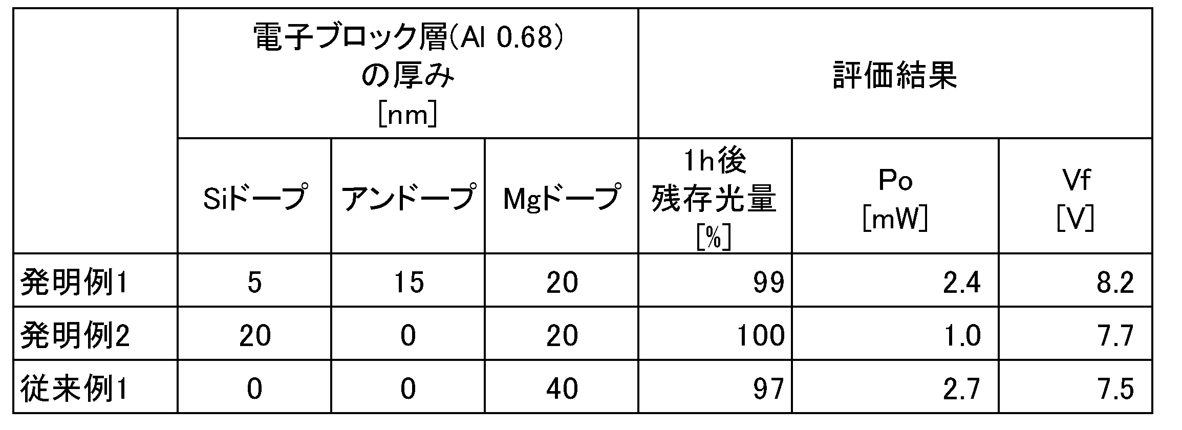
- Table 2 shows the configuration of the electronic blocks of the above-described Invention Examples 1 and 2 and Conventional Example 1. Moreover, the evaluation result mentioned later is also shown collectively.
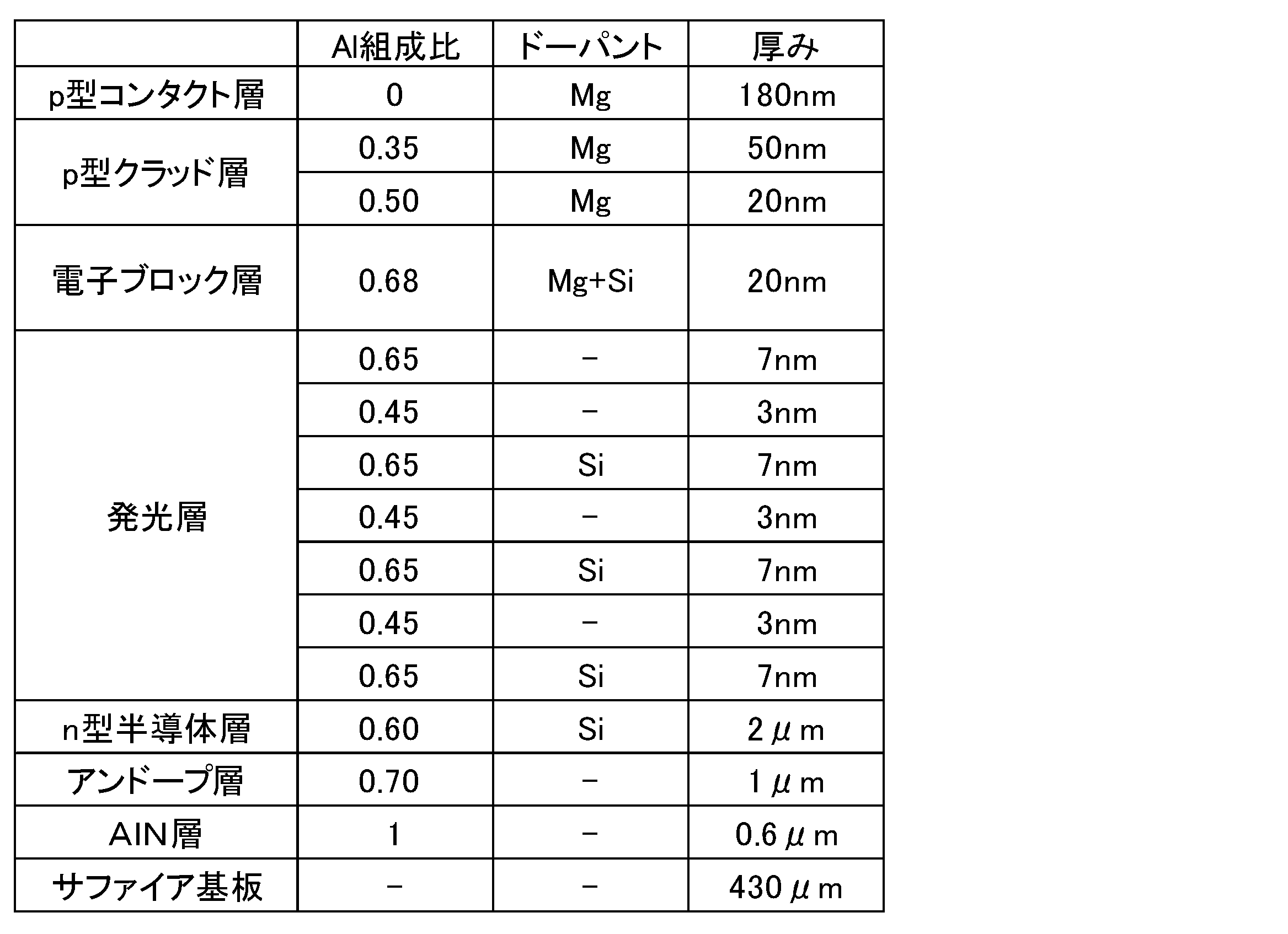
- Invention Example 3 All of the electron blocking layer is doped with Si and Mg so that the total thickness of the electron blocking layer is 20 nm. Further, Al 0 is further interposed between the electron blocking layer and the p-type cladding layer made of Al 0.35 Ga 0.65 N.
- a nitride semiconductor light emitting device according to Invention Example 3 was fabricated under the same conditions as in Invention Example 1 except that a p-type cladding layer composed of .50 Ga 0.50 N and Mg-doped with a thickness of 20 nm was formed. .
- SiH 4 gas was supplied into the chamber at 10 sccm and Cp 2 Mg gas was supplied at 500 sccm.
- the electron blocking layer had a Si concentration of 6.0 ⁇ 10 16 atoms / cm 3 and an Mg concentration of 5.0 ⁇ 10 18 atoms / cm 3 .
- the Mg concentration of the p-type cladding layer made of Al 0.50 Ga 0.50 N was 5.0 ⁇ 10 18 atoms / cm 3 .
- Table 3 shows the layer structure of Invention Example 3.
- Comparative Example 1 A nitride semiconductor light emitting device according to Comparative Example 1 was fabricated under the same conditions as Example 3 except that all of the electron blocking layer was undoped.
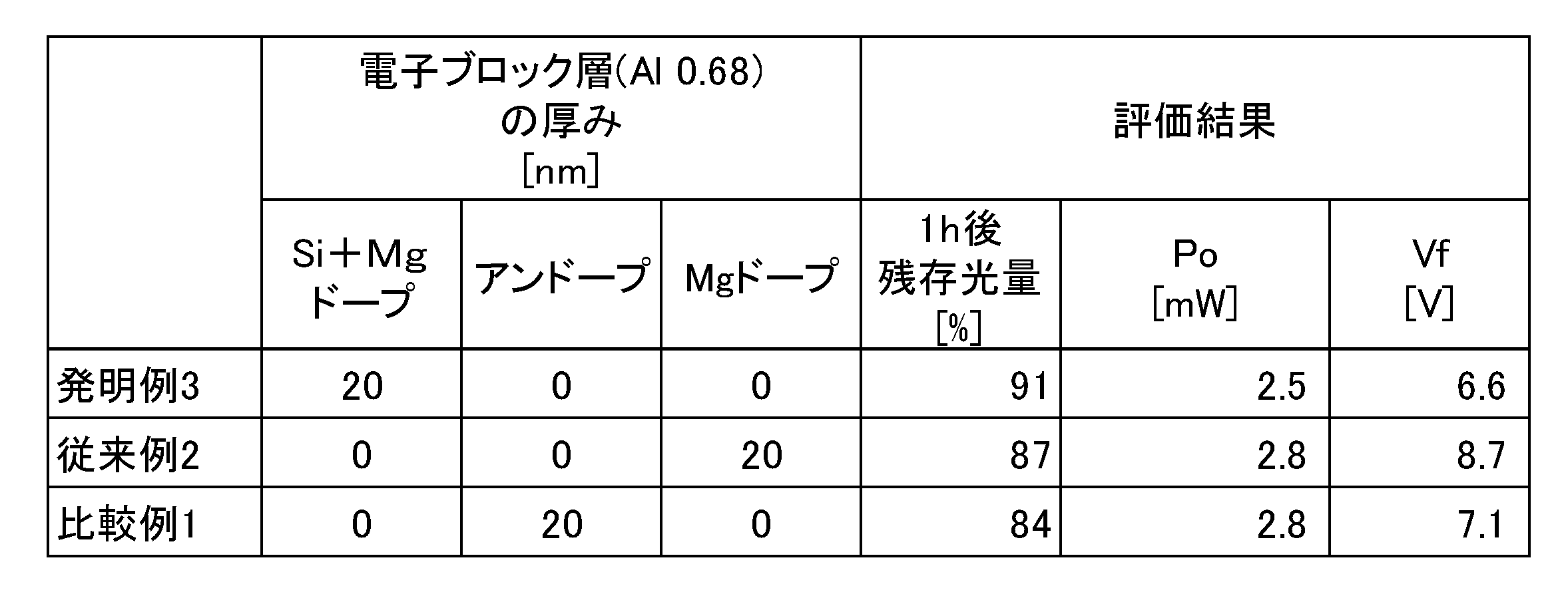
- Table 4 shows the structures of the electronic block layers of Invention Example 3, Comparative Example 1 and Conventional Example 2 described above. Moreover, the evaluation result mentioned later is also shown collectively.
- Invention Example 5 A Group III nitride semiconductor light-emitting device according to Invention Example 5 was produced in the same manner as Invention Example 4, except that 18 nm on the light-emitting layer side of the electron blocking layer was doped with Mg and the remaining 2 m was doped with Mg and Si. did.
- Invention Example 7 75 nm on the light emitting layer side of the electron blocking layer is doped with Mg, the remaining 5 nm is doped with Mg and Si, and the Si concentration in the region doped with Si and Mg is changed from 2.0 ⁇ 10 18 atoms / cm 3 to 1.
- a Group III nitride semiconductor light-emitting device according to Invention Example 7 was produced in the same manner as in Invention Example 6, except that it was increased to 0 ⁇ 10 19 atoms / cm 3 .
- Table 6 below shows the configuration of the electronic blocks of the above invention examples 4 to 7 and comparative example 2. Inventive Examples 4 to 7 and Comparative Example 2 were evaluated in the same manner as in Experimental Example 1. Table 6 also shows the evaluation results.
- a group III nitride semiconductor light-emitting device having a device lifetime superior to that of the prior art and a method for manufacturing the same can be provided, which is useful.
- Substrate 10A Main surface 20 of substrate AlN layer 30 n-type semiconductor layer 40 light emitting layer 41 well layer 42 barrier layer 50 electron blocking layer 50a Si-containing impurity doped region layer 50b undoped region layer 50c p-type impurity doped region layer 50d p-type impurity Doped region layer 60 p-type semiconductor layer 61 p-type cladding layer 62 p-type contact layer 70 n-type electrode 80 p-type electrode 100 Group III nitride semiconductor device
Landscapes
- Led Devices (AREA)
- Recrystallisation Techniques (AREA)
- Semiconductor Lasers (AREA)
- Chemical Vapour Deposition (AREA)
Abstract
従来よりも優れた素子寿命を有するIII族窒化物半導体発光素子およびその製造方法を提供する。 本発明のIII族窒化物半導体発光素子100は、n型半導体層30と、少なくともAlを含む発光層40と、電子ブロック層50と、p型半導体層60とをこの順に有し、発光層40は、井戸層41と障壁層42とを有する量子井戸構造を備え、電子ブロック層50は、発光層40に隣接し、かつ、障壁層42およびp型半導体層60よりもよりもAl組成の大きな層からなり、電子ブロック層51は、Si含有不純物ドープ領域層51aを含むことを特徴とする。
Description
本発明は、III族窒化物半導体発光素子およびその製造方法に関し、特に、優れた素子寿命を有するIII族窒化物半導体発光素子およびその製造方法に関する。
従来、Al、Ga、In等とNとの化合物からなるIII族窒化物半導体は、紫外光発光素子の材料として用いられている。中でも、高Al組成のAlGaNからなるIII族窒化物半導体は、紫外発光素子や発光波長300nm以下の深紫外光発光素子(DUV-LED)に用いられている。
III族窒化物半導体発光素子に要求される特性として、例えば高外部量子効率特性や低抵抗特性などが挙げられる。本願出願人は、特許文献1において、量子井戸構造の発光層とp型クラッド層との間に、電子ブロック層と呼ばれる電子のエネルギー障壁となる層を形成することにより、発光効率を高めることを先に提案している。電子ブロック層は、発光層の量子井戸層に対して障壁となり、電子が過剰に流れていくのを防ぐことによって、キャリアの注入効率を向上することができるのである。
また、特許文献2には、窒化物系化合物半導体を用いた半導体発光装置において、p型クラッド層のp側光ガイド層との境界側に、前記p型クラッド層全体に比べて局所的に高濃度ドーピングされた高濃度ドーピング層を設けた半導体発光装置が開示されている。特許文献2によると、p型クラッド層の一部にp型クラッド層全体に比べて局所的に高濃度ドーピングされた高濃度ドーピング層を設けることによって、p型クラッド層の結晶性を劣化させることなく正孔濃度(ホール濃度)を高めることが可能になり、それによって、直列抵抗を低減してしきい値電流密度を低減することができる。
特許文献1および特許文献2に記載の技術により、III族窒化物半導体発光素子の外部量子効率特性や抵抗特性を改善することができる。しかしながら、外部量子効率特性および抵抗特性の改善以外にも、III族窒化物半導体発光素子の素子寿命特性の改善が希求されており、寿命の点で改善の余地が残されている。
そこで、本発明の目的は、従来よりも優れた素子寿命を有するIII族窒化物半導体発光素子およびその製造方法を提供することを目的とする。
本発明者らは、上記課題を解決する方途について鋭意検討し、III族窒化物半導体発光素子における、発光層よりp型半導体層側に位置する電子ブロック層のドーパントに着目した。ここで、III族窒化物半導体発光素子のp型半導体層側にドープするp型のドーパントとしては、Mgを用いることが一般的である。本発明者らは、p型半導体層側にドープされたMgの発光層への拡散が、III族窒化物半導体発光素子の寿命特性に影響するのではないかと考えた。そこで、活性層とp型半導体層との間の電子ブロック層にSi含有不純物ドープ領域層を設けることにより、III族窒化物半導体発光素子の寿命を改善できることを知見し、本発明を完成するに至った。
すなわち、本発明の要旨構成は以下の通りである。
(1)n型半導体層と、少なくともAlを含む発光層と、電子ブロック層と、p型半導体層とをこの順に有するIII族窒化物半導体発光素子において、前記発光層は、井戸層と障壁層との積層による量子井戸構造を備え、前記電子ブロック層は、前記発光層に隣接し、かつ、前記障壁層および前記p型半導体層よりもAl組成の大きな層からなり、前記電子ブロック層は、Si含有不純物ドープ領域層を含むことを特徴とするIII族窒化物半導体発光素子。
(1)n型半導体層と、少なくともAlを含む発光層と、電子ブロック層と、p型半導体層とをこの順に有するIII族窒化物半導体発光素子において、前記発光層は、井戸層と障壁層との積層による量子井戸構造を備え、前記電子ブロック層は、前記発光層に隣接し、かつ、前記障壁層および前記p型半導体層よりもAl組成の大きな層からなり、前記電子ブロック層は、Si含有不純物ドープ領域層を含むことを特徴とするIII族窒化物半導体発光素子。
(2)前記電子ブロック層は、前記Si含有不純物ドープ領域層よりも前記p型半導体層側にp型不純物ドープ領域層を更に含む、前記(1)に記載のIII族窒化物半導体発光素子。
(3)前記電子ブロック層は、アンドープ領域層を更に含む、前記(1)または(2)に記載のIII族窒化物半導体発光素子。
(4)前記アンドープ領域層は、前記Si含有不純物ドープ領域層と、前記p型不純物ドープ領域層との間に位置する、前記(3)に記載のIII族窒化物半導体発光素子。
(5)前記Si含有不純物ドープ領域層は、前記発光層に隣接する、前記(1)~(4)のいずれかに記載のIII族窒化物半導体発光素子。
(6)前記p型半導体層は、AlxGa1-xN(0≦x≦0.1)からなるp型コンタクト層を有する前記(1)~(5)のいずれかに記載のIII族窒化物半導体発光素子。
(7)前記p型半導体層は、前記電子ブロック層よりもAl組成の小さく、前記p型コンタクト層よりもAl組成の大きいp型クラッド層を、前記電子ブロック層と、前記p型コンタクト層との間に更に有する、前記(6)のいずれかに記載のIII族窒化物半導体発光素子。
(8)前記p型クラッド層はAlyGa1-yN(0.20≦y)である、前記(7)に記載のIII族窒化物半導体発光素子。
(9)前記Si含有不純物ドープ領域層に含まれるSiの不純物濃度が、5×10¹⁶atoms/cm3~1×1018atoms/cm3である前記(1)~(8)のいずれか1項に記載のIII族窒化物半導体発光素子。
(10)前記障壁層はAlbGa1-bN(0.4≦b≦0.95)であり、前記電子ブロック層はAlzGa1-zN(b<z≦1)である、前記(1)~(9)のいずれかに記載のIII族窒化物半導体発光素子。
(11)前記Si含有不純物ドープ領域のドーパントは、Siのみである前記(1)~(10)のいずれかに記載のIII族窒化物半導体発光素子。
(12)前記Si含有不純物ドープ領域のドーパントは、SiおよびMgである前記(1)~(10)のいずれかに記載のIII族窒化物半導体発光素子。
(13)前記発光層から放射される光が、中心波長が300nm以下の深紫外光である、前記(1)~(12)のいずれかに記載のIII族窒化物半導体発光素子。
(14)n型半導体層を形成するn型半導体層形成工程と、前記n型半導体層上に、少なくともAlを含み、井戸層および障壁層の積層による量子井戸構造の発光層を形成する発光層形成工程と、前記発光層上に、前記障壁層よりAl組成の大きい電子ブロック層を形成する電子ブロック層形成工程と、前記電子ブロック層上に、p型半導体層を形成するp型半導体層形成工程と、を含むIII族窒化物半導体発光素子の製造方法において、前記電子ブロック層形成工程では、Si含有不純物をドープしたSi含有不純物ドープ領域層を形成することを特徴とする、III族窒化物半導体発光素子の製造方法。
(15)n型半導体層と、少なくともAlを含む発光層と、電子ブロック層と、p型半導体層とをこの順に有するIII族窒化物半導体発光素子において、前記発光層は、井戸層と障壁層との積層による量子井戸構造を備え、前記電子ブロック層は、前記発光層に隣接し、かつ、前記障壁層および前記p型半導体層よりもAl組成の大きな層からなり、前記電子ブロック層は、Si含有不純物ドープ領域層を含み、前記電子ブロック層は、前記Si含有不純物ドープ領域層よりも前記発光層側にp型不純物ドープ領域層を更に含むことを特徴とするIII族窒化物半導体発光素子。
(16)前記Si含有不純物ドープ領域層は、前記p型半導体層に隣接する、前記(15)に記載のIII族窒化物半導体発光素子。
(17)前記障壁層はAlbGa1-bN(0.4≦b≦0.95)であり、前記電子ブロック層はAlzGa1-zN(b<z≦1)である、前記(15)または(16)に記載のIII族窒化物半導体発光素子。
(18)前記p型不純物ドープ領域層のドーパントは、Mgである、前記(15)~(17)のいずれかに記載のIII族窒化物半導体発光素子。
(19)前記Si含有不純物ドープ領域層のドーパントは、SiおよびMgである、前記(15)~(18)のいずれかに記載のIII族窒化物半導体発光素子。
(20)前記発光層から放射される光が、中心波長が300nm以下の深紫外光である、前記(15)~(19)のいずれかに記載のIII族窒化物半導体発光素子。
本発明によれば、III族窒化物半導体発光素子のp型半導体層において、電子ブロック層にSi含有不純物ドープ領域層を設けたので、従来よりも優れた素子寿命を有するIII族窒化物半導体発光素子およびその製造方法を提供することができる。
以下、図面を参照して本発明の実施形態について説明する。なお、同一の構成要素には原則として同一の参照番号を付して、説明を省略する。また、各図において、説明の便宜上、基板および各層の縦横の比率を実際の比率から誇張して示している。
(第1実施形態:III族窒化物半導体発光素子100)
図1に示すように、本発明の一実施形態に従うIII族窒化物半導体発光素子100は、n型半導体層30と、少なくともAlを含む発光層40と、電子ブロック層50と、p型半導体層60とをこの順に有する。そして、発光層40は、井戸層41と障壁層42との積層による量子井戸構造を備え、電子ブロック層50は、発光層40に隣接し、かつ、障壁層42およびp型半導体層60よりもAl組成の大きな層からなり、電子ブロック層50は、Si含有不純物ドープ領域層50aを含むことを特徴とする。
図1に示すように、本発明の一実施形態に従うIII族窒化物半導体発光素子100は、n型半導体層30と、少なくともAlを含む発光層40と、電子ブロック層50と、p型半導体層60とをこの順に有する。そして、発光層40は、井戸層41と障壁層42との積層による量子井戸構造を備え、電子ブロック層50は、発光層40に隣接し、かつ、障壁層42およびp型半導体層60よりもAl組成の大きな層からなり、電子ブロック層50は、Si含有不純物ドープ領域層50aを含むことを特徴とする。
また、図1に示すように、III族窒化物半導体発光素子100のn型半導体層30を、基板10の表面にAlN層20が設けられたAlNテンプレート基板上に設けることができる。また、III族窒化物半導体発光素子100には、発光層40、電子ブロック層50およびp型半導体層60の一部をエッチング等により除去し、露出したn型半導体層30上に形成したn型電極70と、p型コンタクト層62上に形成したp型電極80とが設けられてもよい。本発明の一実施形態に従うIII族窒化物半導体発光素子100において、n型半導体層30、発光層40、電子ブロック層50およびp型半導体層60が特徴となる構成であり、そのうち、電子ブロック層50が特に特徴となる構成である。上記のサファイア基板10、AlN層20、n型電極70およびp型電極80は一般的な構成とすることができ、具体的な構成は何ら限定されるものではない。なお、III族窒化物半導体発光素子100における各半導体層は、例えばAlGaN材料からなり、また、III族元素としてのAlとGaに対して5%以内の量のInを含んでいてもよい。後述のIII族窒化物半導体発光素子200についても同様である。以下、本発明の特徴となる構成である、n型半導体層30、発光層40、電子ブロック層50およびp型半導体層60についてまず説明する。
n型半導体層30は、少なくともAlを含むIII族窒化物半導体層であり、III族窒化物半導体のpn接合を構成する層であれば、一般的なn型半導体層を用いることができる。前述のとおり、n型半導体層30は、例えばAlGaN材料からなり、また、III族元素としてのAlとGaに対して5%以内の量のInを含んでいてもよい。n型半導体層30には、n型のドーパント(不純物)がドープされ、n型ドーパントとしては、Si,Ge,Sn,S,O,Ti,Zr等を例示することができる。ドーパント濃度は、n型として機能することのできるドーパント濃度であれば特に限定されず、例えば1.0×10¹⁸atoms/cm3~1.0×1020atoms/cm3とすることができる。また、n型半導体層30のAl含有率は、特に制限はなく、一般的な範囲とすることができる。n型半導体層30を単層または複数層から構成することもできる。
発光層40は、n型半導体層30上に設けられる。この発光層40は、少なくともAlを含み、例えばAlaGa1-aN材料(0<a≦1)で形成することができる。ここで、Alの組成は、所望の波長の光を発光するように適切に設定するが、Al組成aが0.35以上(すなわち、0.35≦a≦1)の場合、発光層40から放射される光の中心波長が300nm以下となり、最終的に作製されるIII族窒化物半導体発光素子100はDUV-LEDとなる。
この発光層40は、Al組成の異なるAlGaNからなる井戸層41と障壁層42とを繰り返し形成した多重量子井戸(MQW:Multiple Quantum Well)で構成することができる。井戸層41のAl組成は、例えば0.3~0.8である。障壁層42のAl組成bは、井戸層41のAl組成より大きく、例えば0.40~0.95である。また、井戸層41および障壁層42の繰り返し回数は、例えば1~10回である。発光層40の、n型半導体層30側および電子ブロック層50側(すなわち最初と最後)を障壁層とすることが好ましく、井戸層41および障壁層42の繰り返し回数をnとすると、この場合は「n.5組の井戸層および障壁層」と表記することとする。さらに、井戸層41の厚みは、0.5nm~5nm、障壁層42の厚みは、3nm~30nmとすることができる。
電子ブロック層50は、発光層40に隣接して設けられ、障壁層42のAl組成bおよびp型半導体層60のAl組成よりも大きな層からなる。電子ブロック層50は一般的に、発光層とp型クラッド層との間に設けることにより、電子を堰止めして、電子を発光層40(MQWの場合には井戸層41)内に注入して、電子の注入効率を高めるための層として用いられる。特に、発光層40のAl組成が高い場合には、p型半導体層60のホール濃度が低いため、ホールを発光層40に注入しにくく、一部の電子がp型半導体層60側に流れてしまうが、電子ブロック層50を設けることにより、こうした電子の流れを防止することができる。なお、本発明において、「電子ブロック層」のAl組成zは、発光層40を構成する障壁層42のAl組成bよりも大きく、バンドギャップが大きな層を意味している。対して、「クラッド層」のAl組成は、電子ブロック層のAl組成よりも0.1を超えて小さく、p型コンタクト層よりも0.1を超えて大きいものを指す。後述するが、p型半導体層60はp型クラッド層61を有していても、有していなくてもいずれでもよい。一実施形態においてIII族窒化物半導体発光素子100にp型クラッド層61が設けられる場合、p型クラッド層61のAl組成yは、電子ブロック層50のAl組成zおよびp型コンタクト層62のAl組成xを用いると、x+0.1<y<z-0.1である。なお、中心波長が300nm以下において使用されるp型のAlGaNはAl組成が大きいほど電流が流れにくいため、従来クラッド層として使用されるAl組成は、障壁層のAl組成以下であることが多い。このため、本発明における電子ブロック層と従来技術におけるクラッド層とは、障壁層のAl組成を基準として区別することとする。
電子ブロック層50は、例えばAlzGa1-zN材料(b<z≦1)で形成することができる。障壁層42のAl組成にもよるが、例えばこの電子ブロック層50のAl組成は、0.5以上1.0以下(すなわち、b<z≦1かつ0.5≦z)とすることが好ましい。これにより、井戸層41への電子の注入効率を高めることができる。また、電子ブロック層50全体の厚みは、例えば6nm~60nmであることが好ましい。電子ブロック層51の厚さが6nmより薄くても60nmを超えても、出力の大幅な減少がみられるためである。なお、電子ブロック層50の厚みは、障壁層42の厚みよりは厚いことが好ましい。電子ブロック層にSi含有不純物ドープ領域層50aを設ける技術的意義については後述する。なお、電子ブロック層の一部または全部にはSiに加えてp型ドーパントをドープしてもよく、その場合、p型ドーパントとしては、Mg,Zn,Ca,Be,Mn等を例示することができる。p型半導体層60全体の平均ドーパント濃度は、p型として機能することのできるドーパント濃度であれば特に限定されず、例えば1.0×10¹⁸atoms/cm3~5.0×1021atoms/cm3とすることができる。
本実施形態において、p型半導体層60はp型コンタクト層62を少なくとも有する。該p型コンタクト層62は、Al組成xが0≦x≦0.1である、p型のAlxGa1-xN材料とすることができる。p型コンタクト層62は、この上に形成されるp型電極80と電子ブロック層50との間の接触抵抗を低減するための層であり、p型コンタクト層62上に形成されるp型電極80との接触抵抗を十分に低減することができる。特に、x=0(すなわち、GaN)とすることが好ましい。このp型コンタクト層62をp型とするためのドーパントとしては、マグネシウム(Mg)や亜鉛(Zn)を用いることができる。p型コンタクト層62の厚みを5nm以上200nm以下とすることができる。図示しないが、p型コンタクト層62は、Al組成、ドーパント種、ドーパント濃度、形成時のキャリアガス種などのいずれか1つまたは複数要素を変えた、複数層構造としてもよい。
ここで、電子ブロック層50にSi含有不純物ドープ領域層50aを設けることが本発明において肝要である。なお、電子ブロック層50全体をSi含有不純物ドープ領域層50aとしてもよい(図1)。実施例において後述するが、Si含有不純物ドープ領域層50aを設けることにより、III族窒化物半導体発光素子100の素子寿命を改善することができることが、本発明者らの実験結果により明らかとなったのである。
素子寿命を向上することができる理由が理論的に明らかになったわけではないが、本発明者らはその理由を以下のように考えている。すなわち、p型半導体層にドープされるMgは、発光層に拡散しやすく、Mg起因の欠陥が発光層に生じるために、それが原因となって素子寿命が低下すると考えられる。一方、通常n型ドーパントとして用いられるSiは、発光層に拡散しづらく、またMgの拡散を抑制できると考えられる。そこで、発光層とp型半導体層の間の電子ブロック層にSiをドープすることにより、Mg起因の欠陥をトラップできるのではないかと本発明者らは考えている。なお、代表的なp型ドーパントとしてMgの例を用いて説明したが、他のp型不純物を用いてp型半導体層60を形成しても、Si含有不純物ドープ領域層50aを設けることで、同様の現象が生じる。このように、電子ブロック層50にSi含有不純物ドープ領域層50aを設けることで、素子寿命を向上することができたのだと推測される。
本実施形態において、Si含有不純物ドープ領域層50aのドーパントは、Siを含有する不純物であればよく、Siのみとすることができるし、SiおよびMgとすることもできる。Si含有不純物ドープ領域層50aのドーパントがSiのみである場合、Siの不純物濃度を、5×10¹⁶atoms/cm3~1×1018atoms/cm3とすることができ、5×1016atoms/cm3~1×1017atoms/cm3とすることが好ましく、5×1016atoms/cm3~6×1016atoms/cm3とすることがより好ましい。
一方、Mgをドープすることでホール注入効率を高めて、発光出力を維持しまた順方向電圧を低減しつつ、SiをドープすることでMgの発光層への拡散を抑制し、寿命の悪化を抑制することができる。そのため、Si含有不純物ドープ領域のドーパントを、SiおよびMgとすることも好ましい。この場合、Siの不純物濃度の好適範囲はSiのみをドープする場合と同様であり、Mgの不純物濃度については、1×10¹⁸atoms/cm3~1×1020atoms/cm3とすることができる。また、両者の不純物濃度の合計を2×1018atoms/cm3~1×1020atoms/cm3とすることができる。
以上のとおり、本実施形態に従うIII族窒化物半導体発光素子100は、電子ブロック層50にSi含有不純物ドープ領域層50aを設けたので、従来よりも優れた素子寿命を有するIII族窒化物半導体発光素子を実現することができる。
ここで、図2(A)に示すように、本実施形態において、電子ブロック層50は、Si含有不純物ドープ領域層50aよりもp型半導体層60側にp型不純物ドープ領域層50cを更に含むことが好ましい。なお、p型不純物ドープ領域層50cは、Si含有不純物ドープ領域層50aとp型半導体層60との間に位置する。p型不純物ドープ領域層50cを設けることにより、p型不純物がドープされてホール注入効率が高まるため、順方向電圧を低減することができる。なお、p型不純物ドープ領域層50cのドーパントは特に限定されないが、Mgとすることが好ましい。また、p型不純物ドープ領域層50cを設ける場合、その厚みを0nm超60nm以下とすることができ、10nm以上60nm以下とすることが好ましく、20nm以上60nm以下とすることがより好ましい。
また、電子ブロック層50は、アンドープ領域層50bを更に含むことが好ましく、図2(B)に示すように、アンドープ領域層50bは、Si含有不純物ドープ領域層50aと、p型不純物ドープ領域層50cとの間に位置することがより好ましい。Si不純物ドープ層を薄く設けると、p型不純物の発光層への拡散距離が短くなり、寿命の改善率は小さくなるが、発光出力の低下を抑制することができる。そこで、アンドープ領域層50bをSi含有不純物ドープ領域層50aと、p型不純物ドープ領域層50cとの間に挿入することで、Siドープ層の厚さを適切にしつつ、p型不純物の発光層への距離を保って、電子ブロック層へのSiドープに起因する発光出力の低減および順方向電圧の上昇を抑制しつつ、素子寿命を改善することができる。
また、電子ブロック層50にアンドープ領域層が複数設けられてもよく、例えば図2(C)に示すように、電子ブロック層50は第1のアンドープ層50b1、Si含有不純物ドープ領域層50a、第2のアンドープ層50b2、p型不純物ドープ領域層50cをこの順に含んでもよい。一方、図2(A),(B)に示すとおり、Si含有不純物ドープ領域層は、発光層40に隣接することも好ましい。かかる位置関係とすることで、前述のp型不純物拡散の抑制効果がより確実となる。
なお、アンドープ領域層が「アンドープ」であるとは、MgやSi等の特定の不純物を意図的には添加していない層であり、不可避的な不純物の混入はあってよい。本発明では、電気的にp型またはn型として機能せず、キャリア密度が小さいもの(例えば4×10¹⁶/cm3未満)をアンドープ領域層とする。アンドープ領域層50bの厚みは、1nm~60nmとすることができ、5nm~50nmとすることが好ましい。電子ブロック層50がSi含有不純物ドープ領域層、アンドープ領域層およびp型不純物ドープ領域層を有する場合、電子ブロック層50全体の厚みを60nm以下とした上で、Si含有不純物ドープ領域層50aの厚みを1~20nm(好ましくは5~10nm)、p型不純物ドープ領域層50cの厚みを1~20nm(好ましくは5~10nm)とし、残りをアンドープ領域層50bとすることが特に好ましい。
なお、本実施形態に従うIII族窒化物半導体発光素子100において、p型クラッド層は任意であり、設けなくてもよい。すなわち、図2(A),(B)に示すように、p型半導体層60を、p型コンタクト層62のみから構成することができる。一方、図2(D)に示すように、p型半導体層60は、電子ブロック層50よりもAl組成の小さく、障壁層42よりもAl組成の小さいp型クラッド層61を、電子ブロック層50と、p型コンタクト層62との間に更に有してもよい。この場合、電子ブロック層50とp型コンタクト層62のバンドギャップ差を分割することで、ホール注入効率を向上することができるため、p型クラッド層61を設けることにより、III族窒化物半導体発光素子100の発光出力および順方向電圧を改善することができる。なお、p型クラッド層52を設ける場合、その厚みは、2nm~300nmとすることができる。この場合、p型クラッド層61を、AlyGa1-yN(0.20≦y<b)とすることができ、p型クラッド層61Al組成yを0.35≦y<bとすることもできる。なお、図示しないが、p型クラッド層61は、Al組成を変えた複数層構造としてもよい。この場合、発光層側のp型クラッド層を第1p型クラッド層、p型コンタクト層側のp型クラッド層を第2p型クラッド層とすると、第1p型クラッド層のAl組成を、第2p型クラッド層とのAl組成よりも大きくすることが好ましい。
以下に、図1に示した基板10、AlN層20、n型電極70およびp型電極80について、それらの具体的な態様を例示的に説明するが、種々の変形が可能である。既述のとおり、本発明に従う実施形態において、図1に示したサファイア基板10、AlN層20、n型電極70およびp型電極80は、本発明を何ら限定するものではない。
III族窒化物半導体発光素子100の基板10として、サファイア基板を用いることができる。サファイア基板の表面にエピタキシャル成長させたAlN層20が設けられたAlNテンプレート基板を用いてもよい。サファイア基板としては、任意のサファイア基板を用いることができ、オフ角の有無は任意であり、オフ角が設けられている場合の傾斜方向の結晶軸方位は、m軸方向またはa軸方向のいずれでもよい。例えば、サファイア基板の主面を、C面が0.5度のオフ角θで傾斜した面とすることができる。AlNテンプレート基板を用いる場合、サファイア基板表面のAlN層の結晶性が優れていることが好ましい。また、AlNテンプレート基板の表面に、アンドープのAlGaN層が設けられていることも好ましい。
n型電極70は、例えばTi含有膜およびこのTi含有膜上に形成されたAl含有膜を有する金属複合膜とすることができ、その厚み、形状およびサイズは、発光素子の形状およびサイズに応じて適宜選択することができる。また、p型電極80についても、例えばNi含有膜およびこのNi含有膜上に形成されたAu含有膜を有する金属複合膜とすることができ、その厚み、形状およびサイズは、発光素子の形状およびサイズに応じて適宜選択することができる。
(第2実施形態:III族窒化物半導体発光素子200)
前述の第1実施形態により、III族窒化物半導体発光素子100の素子寿命を改善することができる。本発明者らは、III族窒化物半導体発光素子100により素子寿命の向上効果は得られるものの、Si含有不純物ドープ領域層50aを設けない場合に比べて発行出力が僅かながらでも低下する場合があることを知見した。Si含有不純物ドープ領域層50aを設けつつ、素子寿命の改善および出力改善の両立を図るべく、本発明者らは更に鋭意検討し、以下に詳細を説明する第2実施形態に係るIII族窒化物半導体発光素子200を完成した。
前述の第1実施形態により、III族窒化物半導体発光素子100の素子寿命を改善することができる。本発明者らは、III族窒化物半導体発光素子100により素子寿命の向上効果は得られるものの、Si含有不純物ドープ領域層50aを設けない場合に比べて発行出力が僅かながらでも低下する場合があることを知見した。Si含有不純物ドープ領域層50aを設けつつ、素子寿命の改善および出力改善の両立を図るべく、本発明者らは更に鋭意検討し、以下に詳細を説明する第2実施形態に係るIII族窒化物半導体発光素子200を完成した。
すなわち、本発明の第2実施形態に従うIII族窒化物半導体発光素子200は、図3に示すように、n型半導体層30と、少なくともAlを含む発光層40と、電子ブロック層50と、p型半導体層60とをこの順に有する。そして、発光層40は、井戸層41と障壁層42との積層による量子井戸構造を備え、電子ブロック層50は、発光層40に隣接し、かつ、障壁層42およびp型半導体層60よりもAl組成の大きな層からなり、電子ブロック層50は、Si含有不純物ドープ領域層50aを含み、電子ブロック層50は、Si含有不純物ドープ領域層50aよりも発光層40側にp型不純物ドープ領域層50dを更に含むことを特徴とする。第1実施形態と重複する構成については、同一の符号を付し、重複する説明を省略する。
第1実施形態と、第2実施形態とでは、電子ブロック層50が、Si含有不純物ドープ領域層50aよりも発光層40側にp型不純物ドープ領域層50dを更に含む点で異なる。本発明者らの検討によると、p型不純物ドープ領域層50dをこの位置に設けた場合、素子寿命の改善および出力改善を両立できることが実験的に明らかとなった。本発明者らは、このような効果が得られる理由を、後述の実験例2の結果から以下のように考えている。すなわち、Si含有不純物ドープ層50aが発光層40側にあると、発光層40へのSi注入前に正孔が再結合してSi注入が阻害され、出力低下の要因となり得る。ここで、p型不純物濃度(実験例2ではMg)は、電子ブロック層50よりp型コンタクト層62の方が高く、Mg拡散の影響が大きい。そのため、電子ブロック層50により近い側にSi含有不純物ドープ層50aを設けてもMg(すなわちp型不純物)の十分に拡散を抑制でき、素子寿命の改善に効果がある。
本実施形態において、電子ブロック層50はp型不純物ドープ領域層50dおよびSi含有不純物ドープ領域層50aのみから構成することができる。なお、電子ブロック層50は、第1実施形態と同様に、p型半導体層60側にさらにアンドープ領域層50bまたはp型不純物ドープ領域層50cをさらに含んでもよい。ただし、アンドープ領域層50bの挿入は発光出力の観点では出力低下の要因になり得るため、アンドープ領域層50bを設けない方が好ましい。
また、本実施形態において、p型不純物ドープ領域層50dの厚みは特に制限されないが、10nm以上100nm以下とすることが好ましく、15nm以上80nm以下とすることがより好ましい。一方、Si含有不純物ドープ領域層50aの厚みも特に制限されないが、1nm以上40nm以下とすることが好ましく、1nm以上30nm以下とすることがより好ましい。この際、p型不純物ドープ領域層50dの厚みを、Si含有不純物ドープ領域層50aの厚みよりも大きくすることができる。また、p型不純物ドープ領域層50dおよびSi含有不純物ドープ領域層の合計厚みは特に制限されないが、12nm以上100nm以下とすることができる。
また、p型不純物ドープ領域層50dのドーパントは、Mgであることが好ましい。この場合、Mgの不純物濃度については、1×10¹⁸atoms/cm3~1×1020atoms/cm3とすることができる。また、両者の不純物濃度の合計を2×1018atoms/cm3~1×1020atoms/cm3とすることができる。ただし、第1実施形態にも既述のとおり、p型不純物ドープ領域層50dのドーパントをMg以外のp型のドーパントを用いてもよい。
また、Si含有不純物ドープ領域層50aのドーパントは、SiおよびMgであることが好ましい。この場合、Siの不純物濃度を5×10¹⁶atoms/cm3~5×1019atoms/cm3とすることができ、1×1018atoms/cm3~2×1019atoms/cm3以下することがより好ましい。Siの不純物濃度が高くなりすぎると、出力が低下する場合がある。なお、本実施形態では、Siを含有させる位置を発光層から離しているため前述の第1実施形態に比べてSi濃度をより高くすることができている。Siを含有させる位置を発光層から離し、かつ、より高濃度のSiをMgと混在させることでSiによるMgの拡散抑制効果を高めることで、素子寿命の改善および出力改善の両立することができ、好ましい。
そして、Si含有不純物ドープ領域層50aのドーパントがSiおよびMgであるとき、Mgの不純物濃度を1×10¹⁸atoms/cm3~1×1020atoms/cm3とすることができ、5×1018atoms/cm3~5×1019atoms/cm3とすることがより好ましい。また、SiおよびMgの両者の合計不純物濃度を2×1018atoms/cm3~2×1020atoms/cm3とすることができ、5×1018atoms/cm3~5×1019atoms/cm3とすることがより好ましい。ただし、第1実施形態にも既述のとおり、Si含有不純物ドープ領域層50aのドーパントをSiのみとしてもよい。Siのみとする場合も、Siの不純物濃度を5×1016atoms/cm3~5×1019atoms/cm3とすることができ、2×1019atoms/cm3以下とすることがより好ましい。
なお、第1実施形態と同様に、前記障壁層はAlbGa1-bN(0.4≦b≦0.95)であり、前記電子ブロック層はAlzGa1-zN(b<z≦1)とすることができる。また、発光層から放射される光を、中心波長が300nm以下の深紫外光とすることができるのも、第1実施形態と同様である。
また、第1実施形態と同様に、本実施形態においてもp型クラッド層は任意であり、設けなくてもよい。すなわち、p型半導体層60をp型コンタクト層のみから構成することができる。
(第3実施形態:III族窒化物半導体発光素子の製造方法)
本発明の第3実施形態に従うIII族窒化物半導体発光素子100の製造方法は、n型半導体層30を形成するn型半導体層形成工程(図4(E))と、n型半導体層30上に、少なくともAlを含み、井戸層41および障壁層42の積層による量子井戸構造の発光層40を形成する発光層形成工程(図4(F))と、発光層40上に、障壁層42よりAl組成の大きい電子ブロック層50を形成する電子ブロック層形成工程(図4(G))と、電子ブロック層50上に、p型半導体層60を形成するp型半導体層形成工程(図4(H))と、を含む。本実施形態は、電子ブロック層形成工程において、Si含有不純物をドープしたSi含有不純物ドープ領域層50aを形成することを特に特徴とする。以下、第2実施形態の好適な実施形態に従うフローチャートを示す図4を用いて各工程を順次説明するが、前述の第1実施形態または第2実施形態と重複する説明については省略する。
本発明の第3実施形態に従うIII族窒化物半導体発光素子100の製造方法は、n型半導体層30を形成するn型半導体層形成工程(図4(E))と、n型半導体層30上に、少なくともAlを含み、井戸層41および障壁層42の積層による量子井戸構造の発光層40を形成する発光層形成工程(図4(F))と、発光層40上に、障壁層42よりAl組成の大きい電子ブロック層50を形成する電子ブロック層形成工程(図4(G))と、電子ブロック層50上に、p型半導体層60を形成するp型半導体層形成工程(図4(H))と、を含む。本実施形態は、電子ブロック層形成工程において、Si含有不純物をドープしたSi含有不純物ドープ領域層50aを形成することを特に特徴とする。以下、第2実施形態の好適な実施形態に従うフローチャートを示す図4を用いて各工程を順次説明するが、前述の第1実施形態または第2実施形態と重複する説明については省略する。
まず、基板10としてサファイア基板を用意する。基板10の表面10AにAlN層を形成したAlNテンプレート基板を形成することが好ましく、市販のAlNテンプレート基板を用いてもよい(図4(A)~図4(B))。なお、AlN層20は、例えば、有機金属気相成長(MOCVD:Metal Organic Chemical Vapor Deposition)法や分子線エピタキシ(MBE:Molecular Beam Epitaxy)法、スパッタ法などの公知の薄膜成長方法により形成することができる。
AlN層20のAl源としては、トリメチルアルミニウム(TMA)を用いることができる。また、N源としては、アンモニア(NH3)ガスを用いることができる。これらの原料ガスを、キャリアガスとして水素ガスを用いることにより、AlN層20を形成することができる。
なお、AlN層20の成長温度としては、1270℃以上1350℃以下が好ましく、1290℃以上1330℃以下がより好ましい。この温度範囲であれば、続いて熱処理工程を行う場合にAlN層20の結晶性を向上することができる。また、チャンバ内の成長圧力については、例えば5Torr~20Torrとすることができる。より好ましくは、8Torr~15Torrである。
また、NH3ガスなどのV族元素ガスと、TMAガスなどのIII族元素ガスの成長ガス流量を元に計算されるIII族元素に対するV族元素のモル比(以降、V/III比と記載する)については、例えば130以上190以下とすることができる。より好ましくは140以上180以下である。なお、成長温度および成長圧力に応じて最適なV/III比が存在するため、成長ガス流量を適宜設定することが好ましい。
続いて、上述のようにして得られた、サファイア基板10上のAlN層20に対して、このAlN層20の成長温度よりも高温で熱処理を施すことが好ましい。この熱処理工程は、公知の熱処理炉を用いて行うことができる。かかる熱処理を行うことにより、AlN層20の(10-12)面のX線ロッキングカーブの半値幅を400秒以下とし、高い結晶性を実現することができる(図4(C))。
その後、図4(D)に例示するように、AlN層20上に、アンドープのAlGaN層20’を形成することも好ましい。Al源としてTMA、Ga源としてトリメチルガリウム(TMG)、N源としてNH3ガスを用いることで、AlGaN材料からなる層を形成することができ、以下に説明するn型半導体層、発光層、電子ブロック層およびp型半導体層の形成についても同様である。これらの原料ガスを、キャリアガスとして水素ガスもしくは窒素ガスまたは両者の混合ガスを用いてチャンバ内に供給すればよく、一般的には水素ガスが用いられる。また、NH3ガスなどのV族元素ガスと、TMAガスなどのIII族元素ガスの成長ガス流量を元に計算されるIII族元素に対するV族元素のモル比(以降、V/III比と記載する)については、例えば100以上100000以下とすることができる。より好ましくは300以上30000以下である。成長温度および成長圧力に応じて最適なV/III比が存在するため、成長ガス流量を適宜設定することが好ましいのはAlN層20を形成する場合と同様である。
次に、n型半導体層30を形成するn型半導体層形成工程を行う(図4(E))。n型半導体層30は、AlN層20上に形成することができ、アンドープのAlGaN層20’上に形成することが好ましい。n型ドーパントについては既述のとおりである。
続いて、図4(F)に示すように、発光層40を形成する発光層形成工程を行う。発光層40をMQW構造とする場合には、Al源の流量とGa源の流量の比を適切に変更することにより、MQW構造を有する発光層40を形成することができる。発光層40をAlaGa1-aN材料(0<a≦1)で形成する場合、AlaGa1-aN材料の成長温度としては、1000℃以上1400℃以下が好ましく、1050℃以上1350℃以下がより好ましい。
次に、図4(G)に示すように、発光層40の上に電子ブロック層50を形成する電子ブロック層形成工程を行う。上述のように、電子ブロック層50は、Si含有不純物をドープしたSi含有不純物ドープ領域層50aを含む。また、前述のとおり、電子ブロック層50が、p型不純物ドープ領域層50cを更に含む2層構造とすることが好ましく、Si含有不純物ドープ領域層50aと、p型不純物ドープ領域層50cとの間にアンドープ領域層50bを更に有する3層構造とすることも好ましい。
Si含有不純物ドープ領域層50aを形成するためのドーパントとしては、Si単独またはSiおよびMgとすることができる。Si源としては、モノシラン(SiH4)などを用いることができ、Mg源としては、シクロペンタジニエルマグネシウム(CP2Mg)を用いることができる。SiおよびMgを混合してドープする場合には、両者の混合ガスをチャンバに供給すればよい。
また、p型不純物ドープ領域層50cを形成するためのドーパントとしては、MgやZnを用いることができる。Mg源はCP2Mgを用いることができ、Zn源としては、ZnCl2を用いることができる。
電子ブロック層50をAlzGa1-zN材料(b<z≦1)で形成する場合、電子ブロック層50の形成は、キャリアガスとして水素を主成分とするガスを用いることができる。原料ガスは既述のとおりTMA、TMGおよびNH3ガスであり、さらに、Si含有不純物ドープ領域層50a、アンドープ領域層50bおよびp型不純物ドープ領域層50cに応じた不純物ガスを用いる。
なお、電子ブロック層50の成長温度としては、1000℃以上1400℃以下が好ましく、1050℃以上1350℃以下がより好ましい。また、チャンバ内の成長圧力については、例えば10Torr~760Torrとすることができる。より好ましくは、20Torr~380Torrである。
次に、図4(H)に示すように、電子ブロック層50上にp型半導体層60を形成する。p型半導体層60は、p型コンタクト層62を有し、該p型コンタクト層62は、p型のAlxGa1-xN材料(0≦x≦0.1)で形成する。p型コンタクト層62をp型とするためのドーパントとしては、p型不純物ドープ領域層50cの場合と同様、Mgや亜鉛Znを用いることができる。Mg源およびZn源も同様である。
p型コンタクト層62を有するp型半導体層60の成長温度としては、800℃以上1400℃以下が好ましく、900℃以上1300℃以下がより好ましい。また、チャンバ内の成長圧力については、例えば10Torr~760Torrとすることができる。より好ましくは、20Torr~600Torrである。キャリアガスとしては、既述のとおり水素ガスもしくは窒素ガスまたは両者の混合ガスを用いることができる。図示しないが、p型コンタクト層62を複数層とする場合、電子ブロック層側のキャリアガスを水素ガスとし、反対側を窒素ガスとすることもできるし、その逆としてもよい。p型クラッド層を設けてもよいのは、既述のとおりである。
最後に、図4(I)に示すように、発光層40、電子ブロック層50およびp型半導体層60の一部をエッチング等により除去し、露出したn型半導体層30上にn型電極70を、p型コンタクト層62上にp型電極80をそれぞれ形成することができる。こうして、本発明の好適な実施形態に係るIII族窒化物半導体発光素子100を作製することができる。
また、図示しないが、第2実施形態に係るIII族窒化物半導体発光素子200を製造するためには、図4(G)を用いて説明した発光層40の上に電子ブロック層50を形成する電子ブロック層形成工程において、p型不純物ドープ領域層50dを発光層40上に形成し、次いでSi含有不純物ドープ領域層50aを形成すればよい。そして、その他の工程については第1実施形態に係るIII族窒化物半導体発光素子100と同様に行えば、III族窒化物半導体発光素子200を製造することができる。
[実験例1]
(発明例1)
以下、実施例を用いて本発明をさらに詳細に説明するが、本発明は以下の実施例に何ら限定されるものではない。図4に示したフローチャートに従って、III族窒化物半導体発光素子を作製した。まず、サファイア基板(直径2インチ、厚さ:430μm、面方位:(0001)、m軸方向オフ角θ:0.5度、テラス幅:100nm、ステップ高さ:0.20nm)を用意した(図4(A))。次いで、MOCVD法により、上記サファイア基板上に中心膜厚0.60μm(平均膜厚0.61μm)のAlN層を成長させ、AlNテンプレート基板とした(図4(B))。その際、AlN層の成長温度は1300℃、チャンバ内の成長圧力は10Torrであり、V/III比が163となるようにアンモニアガスとTMAガスの成長ガス流量を設定した。V族元素ガス(NH3)の流量は200sccm、III族元素ガス(TMA)の流量は53sccmである。なお、AlN層の膜厚については、光干渉式膜厚測定機(ナノスペックM6100A;ナノメトリックス社製)を用いて、ウェーハ面内の中心を含む、等間隔に分散させた計25箇所の膜厚を測定した。
(発明例1)
以下、実施例を用いて本発明をさらに詳細に説明するが、本発明は以下の実施例に何ら限定されるものではない。図4に示したフローチャートに従って、III族窒化物半導体発光素子を作製した。まず、サファイア基板(直径2インチ、厚さ:430μm、面方位:(0001)、m軸方向オフ角θ:0.5度、テラス幅:100nm、ステップ高さ:0.20nm)を用意した(図4(A))。次いで、MOCVD法により、上記サファイア基板上に中心膜厚0.60μm(平均膜厚0.61μm)のAlN層を成長させ、AlNテンプレート基板とした(図4(B))。その際、AlN層の成長温度は1300℃、チャンバ内の成長圧力は10Torrであり、V/III比が163となるようにアンモニアガスとTMAガスの成長ガス流量を設定した。V族元素ガス(NH3)の流量は200sccm、III族元素ガス(TMA)の流量は53sccmである。なお、AlN層の膜厚については、光干渉式膜厚測定機(ナノスペックM6100A;ナノメトリックス社製)を用いて、ウェーハ面内の中心を含む、等間隔に分散させた計25箇所の膜厚を測定した。
次いで、上記AlNテンプレート基板を熱処理炉に導入し、10Paまで減圧後に窒素ガスを常圧までパージすることにより炉内を窒素ガス雰囲気とした後に、炉内の温度を昇温してAlNテンプレート基板に対して熱処理を施した(図4(C))。その際、加熱温度は1650℃、加熱時間は4時間とした。
続いて、MOCVD法により、アンドープのAlGaN層として、Al0.7Ga0.3Nからなる層厚1μmのアンドープAl0.7Ga0.3N層を形成した(図4(D))。次に、n型半導体層として、Al0.62Ga0.38Nからなり、Siドープした層厚2μmのn型Al0.62Ga0.38N層を上記AlGaN層上に形成した(図4(E))。なお、SIMS分析の結果、n型半導体層のSi濃度は1.0×10¹⁹atoms/cm3である。
続いて、n型半導体層上に、Al0.45Ga0.55Nからなる層厚3nmの井戸層およびAl0.65Ga0.35Nからなる層厚7nmの障壁層を交互に3.5組繰り返して積層した発光層を形成した(図4(F))。3.5組の0.5は、発光層の最初と最後を障壁層としたことを表す。
その後、発光層上に、水素ガスをキャリアガスとして、Al0.68Ga0.32Nからなる層厚40nmの電子ブロック層を形成した(図4(G))。電子ブロック層の形成にあたり、はじめの5nm(Si含有不純物ドープ領域層に相当)はモノシラン(SiH4)ガスを10sccmでチャンバ内に供給し、次の15nm(アンドープ領域層に相当)ではドーパントガスの供給を止め、残り20nm(p型不純物ドープ領域層に相当)ではMgをドープした。なお、SIMS分析の結果、Si含有不純物ドープ領域層のSi濃度は6.0×10¹⁶atoms/cm3であり、アンドープ領域層の不純物濃度は4.0×1016atoms/cm3以下であり、p型不純物ドープ領域層のMg濃度は5.0×1018atoms/cm3であった。
さらに、Al0.35Ga0.65Nからなり、Mgドープした層厚50nmのp型クラッド層を形成した。続いて、GaNからなり、Mgドープした層厚180nmのp型コンタクト層を形成した。なお、層厚180nmの内の、電極に接する厚さ30nmの領域においては、TMGガスの流量を減らしてMgの存在確率を上げ、かつ、成長速度を落とすことにより高Mg濃度の層とした(図4(H))。SIMS分析の結果、このp型クラッド層のMg濃度は1.0×10¹⁹atoms/cm3であり、p型クラッド層側の層厚150nm部分のp型コンタクト層のMg濃度は3.0×1019atoms/cm3であり、高Mg濃度とした残り30nm部分のMg濃度は1.2×1020atom/cm3であった。
その後、p型コンタクト層の上にマスクを形成してドライエッチングによるメサエッチングを行い、n型半導体層を露出させた。次いで、p型コンタクト層上に、Ni/Auからなるp型電極を形成し、露出したn型半導体層上には、Ti/Alからなるn型電極を形成した。なお、p型電極のうち、Niの厚みは50Åであり、Auの厚みは1500Åである。また、n型電極のうち、Tiの厚みは200Åであり、Alの厚みは1500Åである。最後に550℃でコンタクトアニール(RTA)を行って、電極を形成した(図4(I))。こうして発明例1に係るIII族窒化物半導体発光素子を作製した。発明例1の層構造を表1に示す。

(発明例2)
電子ブロック層においてアンドープ領域層を形成せず、電子ブロック層のはじめの20nmをSiドープした以外の条件は発明例1と全て同じとして、発明例2に係る窒化物半導体発光素子を作製した。
電子ブロック層においてアンドープ領域層を形成せず、電子ブロック層のはじめの20nmをSiドープした以外の条件は発明例1と全て同じとして、発明例2に係る窒化物半導体発光素子を作製した。
(従来例1)
電子ブロック層の全てをMgドープとした以外の条件は、発明例1と全て同じとして、従来例1に係る窒化物半導体発光素子を作製した。
電子ブロック層の全てをMgドープとした以外の条件は、発明例1と全て同じとして、従来例1に係る窒化物半導体発光素子を作製した。
以上の発明例1~2および従来例1の、電子ブロックの構成を以下の表2に示す。また、後述の評価結果も併せて示す。
(発明例3)
電子ブロック層の全てをSiおよびMgドープして、電子ブロック層全体の層厚を20nmとし、電子ブロック層とAl0.35Ga0.65Nからなるp型クラッド層との間に更にAl0.50Ga0.50Nからなり、Mgドープした層厚20nmのp型クラッド層を形成した以外の条件は、発明例1と全て同じとして、発明例3に係る窒化物半導体発光素子を作製した。なお、電子ブロックへのドープにあたり、SiH4ガスを10sccmで、Cp2Mgガスを500sccmでチャンバ内に供給した。電子ブロック層のSi濃度は6.0×10¹⁶atoms/cm3であり、Mg濃度は5.0×1018atoms/cm3であった。また、Al0.50Ga0.50Nからなるp型クラッド層のMg濃度は5.0×1018atoms/cm3であった。発明例3の層構造を表3に示す。
電子ブロック層の全てをSiおよびMgドープして、電子ブロック層全体の層厚を20nmとし、電子ブロック層とAl0.35Ga0.65Nからなるp型クラッド層との間に更にAl0.50Ga0.50Nからなり、Mgドープした層厚20nmのp型クラッド層を形成した以外の条件は、発明例1と全て同じとして、発明例3に係る窒化物半導体発光素子を作製した。なお、電子ブロックへのドープにあたり、SiH4ガスを10sccmで、Cp2Mgガスを500sccmでチャンバ内に供給した。電子ブロック層のSi濃度は6.0×10¹⁶atoms/cm3であり、Mg濃度は5.0×1018atoms/cm3であった。また、Al0.50Ga0.50Nからなるp型クラッド層のMg濃度は5.0×1018atoms/cm3であった。発明例3の層構造を表3に示す。
(従来例2)
電子ブロック層の全てをMgドープとした以外の条件は、発明例3と全て同じとして、従来例2に係る窒化物半導体発光素子を作製した。
電子ブロック層の全てをMgドープとした以外の条件は、発明例3と全て同じとして、従来例2に係る窒化物半導体発光素子を作製した。
(比較例1)
電子ブロック層の全てをアンドープとした以外の条件は、発明例3と全て同じとして、比較例1に係る窒化物半導体発光素子を作製した。
電子ブロック層の全てをアンドープとした以外の条件は、発明例3と全て同じとして、比較例1に係る窒化物半導体発光素子を作製した。
以上の発明例3、比較例1および従来例2の電子ブロック層の構造を表4に示す。また、後述の評価結果も併せて示す。
<発光寿命の評価>
発明例1について、作製したフリップチップ型のIII族窒化物半導体発光素子を、積分球により電流20mAのときの発光出力Po(mW)を測定し、さらに1時間通電後の残存出力(1時間通電後の出力/初期発光出力)を測定したところ、初期の出力に対して99%であった。結果を表3に示す。発明例2,3、比較例1、従来例1,2についても、同様に1時間経過後の残存出力を測定したところ、表3,4のとおりであった。
発明例1について、作製したフリップチップ型のIII族窒化物半導体発光素子を、積分球により電流20mAのときの発光出力Po(mW)を測定し、さらに1時間通電後の残存出力(1時間通電後の出力/初期発光出力)を測定したところ、初期の出力に対して99%であった。結果を表3に示す。発明例2,3、比較例1、従来例1,2についても、同様に1時間経過後の残存出力を測定したところ、表3,4のとおりであった。
従来例1と、発明例1,2とを比べると、Siドープ層を設けた発明例1,2では、III族窒化物半導体発光素子の寿命を改善できたことが分かった。同様に、Al0.50Ga0.50Nからなるp型クラッド層を設けた従来例2と、発明例3とを比較すると、Si含有不純物ドープ領域層を設けた発明例3では、寿命を改善できたことが分かった。なお、従来例2と、比較例1とを比べると、電子ブロック層へのMgドープに代えて、アンドープにした場合は、かえって寿命を悪化させてしまうことが分かった。
<発光特性および順方向電圧の評価>
発明例1について、作製したフリップチップ型のIII族窒化物半導体発光素子を、積分球により電流20mAのときの発光出力Po(mW)および順方向電圧Vf(V)をそれぞれ測定したところ、2.4mW、8.2Vであった。発明例2,3、比較例1、従来例1,2についても、同様に発光出力Poおよび順方向電圧Vfを測定したところ、表3,4のとおりであった。
発明例1について、作製したフリップチップ型のIII族窒化物半導体発光素子を、積分球により電流20mAのときの発光出力Po(mW)および順方向電圧Vf(V)をそれぞれ測定したところ、2.4mW、8.2Vであった。発明例2,3、比較例1、従来例1,2についても、同様に発光出力Poおよび順方向電圧Vfを測定したところ、表3,4のとおりであった。
従来例1、発明例1,2を比べると、電子ブロック層内にアンドープ領域層を設けることにより、素子の寿命の改善効果が若干低減するものの、発光出力の低下を抑制できることがわかった。逆に、Siドープ層の厚みを大きくすることで、素子の寿命改善効果を最大化できることがわかった。また、従来例2と、発明例3とを比べると、SiおよびMgをドープすることで、寿命を改善しつつ、順方向電圧を低減できることがわかった。
[実験例2]
上述の実験例1における発明例1~3により、素子寿命等の信頼性の向上効果が確実に得られることが確認された。しかしながら、Siドープ層を設けていない従来例1,2に比べて発光出力が僅かでも低下する場合がある。そこで、発光出力を低下させることなく、信頼性を向上させる実験を以下のとおり行った。
上述の実験例1における発明例1~3により、素子寿命等の信頼性の向上効果が確実に得られることが確認された。しかしながら、Siドープ層を設けていない従来例1,2に比べて発光出力が僅かでも低下する場合がある。そこで、発光出力を低下させることなく、信頼性を向上させる実験を以下のとおり行った。
(発明例4)
電子ブロック層を形成するときに、電子ブロック層全体の層厚を20nmとし、発光層側の15nmをMgドープ層とし、p型半導体層側の残りの5nmにSiおよびMgをドープした。そして、p型半導体層を形成するときに、p型クラッド層を形成せず、p型コンタクト層のみを形成した。その他の条件は、発明例1と全て同じとして、発明例4に係るIII族窒化物半導体発光素子を作製した。なお、電子ブロックへのMgドープおよびSiドープにあたり、Cp2Mgガスを250sccmでチャンバ内に供給して、層厚15nmを形成した後に、さらにSiH4ガスを12sccm追加することで、p型半導体層側の残りの5nmにはMgおよびSiの両方をドープした。SIMS分析の結果、電子ブロック層のMg濃度は、全体を通して2×10¹⁸atoms/cm3であり、SiおよびMgをドープした領域層のSi濃度は2.0×1018atoms/cm3であった。発明例4の層構造を表5に示す。
電子ブロック層を形成するときに、電子ブロック層全体の層厚を20nmとし、発光層側の15nmをMgドープ層とし、p型半導体層側の残りの5nmにSiおよびMgをドープした。そして、p型半導体層を形成するときに、p型クラッド層を形成せず、p型コンタクト層のみを形成した。その他の条件は、発明例1と全て同じとして、発明例4に係るIII族窒化物半導体発光素子を作製した。なお、電子ブロックへのMgドープおよびSiドープにあたり、Cp2Mgガスを250sccmでチャンバ内に供給して、層厚15nmを形成した後に、さらにSiH4ガスを12sccm追加することで、p型半導体層側の残りの5nmにはMgおよびSiの両方をドープした。SIMS分析の結果、電子ブロック層のMg濃度は、全体を通して2×10¹⁸atoms/cm3であり、SiおよびMgをドープした領域層のSi濃度は2.0×1018atoms/cm3であった。発明例4の層構造を表5に示す。
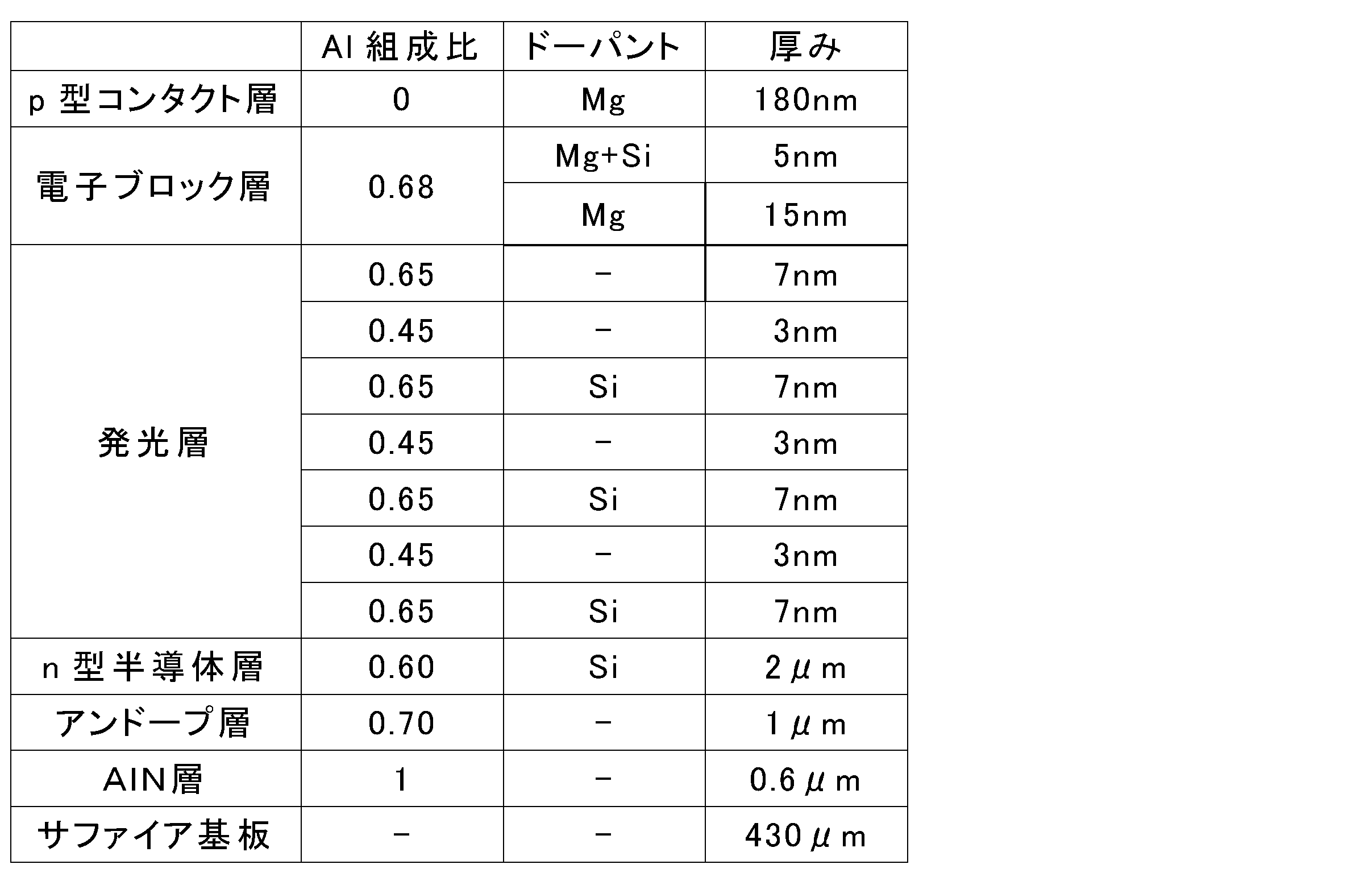
(発明例5)
電子ブロック層の発光層側の18nmにMgをドープし、残りの2mにMgおよびSiをドープした以外は、発明例4と同様にして、発明例5に係るIII族窒化物半導体発光素子を作製した。
電子ブロック層の発光層側の18nmにMgをドープし、残りの2mにMgおよびSiをドープした以外は、発明例4と同様にして、発明例5に係るIII族窒化物半導体発光素子を作製した。
(発明例6)
電子ブロック層の発光層側の60nmにMgをドープし、残りの20mにMgおよびSiをドープした(すなわち、発明例4に対し電子ブロック層の厚さをそれぞれ4倍にした)以外は、発明例4と同様にして、発明例7に係るIII族窒化物半導体発光素子を作製した。
電子ブロック層の発光層側の60nmにMgをドープし、残りの20mにMgおよびSiをドープした(すなわち、発明例4に対し電子ブロック層の厚さをそれぞれ4倍にした)以外は、発明例4と同様にして、発明例7に係るIII族窒化物半導体発光素子を作製した。
(発明例7)
電子ブロック層の発光層側の75nmにMgをドープし、残りの5nmにMgおよびSiをドープし、SiおよびMgをドープした領域のSi濃度を2.0×10¹⁸atoms/cm3から1.0×1019atoms/cm3に増大させた以外は、発明例6と同様にして、発明例7に係るIII族窒化物半導体発光素子を作製した。
電子ブロック層の発光層側の75nmにMgをドープし、残りの5nmにMgおよびSiをドープし、SiおよびMgをドープした領域のSi濃度を2.0×10¹⁸atoms/cm3から1.0×1019atoms/cm3に増大させた以外は、発明例6と同様にして、発明例7に係るIII族窒化物半導体発光素子を作製した。
(比較例2)
電子ブロック層の全てをMgドープとした以外の条件は、発明例4と全て同じとして、
比較例2に係るIII族窒化物半導体発光素子を作製した。
電子ブロック層の全てをMgドープとした以外の条件は、発明例4と全て同じとして、
比較例2に係るIII族窒化物半導体発光素子を作製した。
以上の発明例4~7および比較例2の、電子ブロックの構成を以下の表6に示す。また、発明例4~7および比較例2について、実験例1と同様に評価を行った。表6に、その評価結果を併せて示す。

以上の実験例2の結果から、電子ブロック層の発光層側にMgをドープしたp型不純物領域層を配置し、かつ、p型半導体層側にSi含有不純物ドープ領域層を配置することで、Si含有不純物ドープ領域層を設けない場合に比べても、発光出力の低下なく、むしろ発光出力を増大させつつ、信頼性を向上できることが分かった。
本発明によれば、従来よりも優れた素子寿命を有するIII族窒化物半導体発光素子およびその製造方法を提供することができるため、有用である。
10 基板
10A 基板の主面
20 AlN層
30 n型半導体層
40 発光層
41 井戸層
42 障壁層
50 電子ブロック層
50a Si含有不純物ドープ領域層
50b アンドープ領域層
50c p型不純物ドープ領域層
50d p型不純物ドープ領域層
60 p型半導体層
61 p型クラッド層
62 p型コンタクト層
70 n型電極
80 p型電極
100 III族窒化物半導体素子
10A 基板の主面
20 AlN層
30 n型半導体層
40 発光層
41 井戸層
42 障壁層
50 電子ブロック層
50a Si含有不純物ドープ領域層
50b アンドープ領域層
50c p型不純物ドープ領域層
50d p型不純物ドープ領域層
60 p型半導体層
61 p型クラッド層
62 p型コンタクト層
70 n型電極
80 p型電極
100 III族窒化物半導体素子
Claims (20)
- n型半導体層と、少なくともAlを含む発光層と、電子ブロック層と、p型半導体層とをこの順に有するIII族窒化物半導体発光素子において、
前記発光層は、井戸層と障壁層との積層による量子井戸構造を備え、
前記電子ブロック層は、前記発光層に隣接し、かつ、前記障壁層および前記p型半導体層よりもAl組成の大きな層からなり、
前記電子ブロック層は、Si含有不純物ドープ領域層を含むことを特徴とするIII族窒化物半導体発光素子。 - 前記電子ブロック層は、前記Si含有不純物ドープ領域層よりも前記p型半導体層側にp型不純物ドープ領域層を更に含む、請求項1に記載のIII族窒化物半導体発光素子。
- 前記電子ブロック層は、アンドープ領域層を更に含む、請求項1または2に記載のIII族窒化物半導体発光素子。
- 前記アンドープ領域層は、前記Si含有不純物ドープ領域層と、前記p型不純物ドープ領域層との間に位置する、請求項3に記載のIII族窒化物半導体発光素子。
- 前記Si含有不純物ドープ領域層は、前記発光層に隣接する、請求項1~4のいずれか1項に記載のIII族窒化物半導体発光素子。
- 前記p型半導体層は、AlxGa1-xN(0≦x≦0.1)からなるp型コンタクト層を有する請求項1~5のいずれか1項に記載のIII族窒化物半導体発光素子。
- 前記p型半導体層は、前記電子ブロック層よりもAl組成の小さく、前記p型コンタクト層よりもAl組成の大きいp型クラッド層を、前記電子ブロック層と、前記p型コンタクト層との間に更に有する、請求項6に記載のIII族窒化物半導体発光素子。
- 前記p型クラッド層はAlyGa1-yN(0.2≦y)である、請求項7に記載のIII族窒化物半導体発光素子。
- 前記Si含有不純物ドープ領域層に含まれるSiの不純物濃度が、5×10¹⁶atoms/cm3~1×1018atoms/cm3である請求項1~8のいずれか1項に記載のIII族窒化物半導体発光素子。
- 前記障壁層はAlbGa1-bN(0.4≦b≦0.95)であり、前記電子ブロック層はAlzGa1-zN(b<z≦1)である、請求項1~9のいずれか1項に記載のIII族窒化物半導体発光素子。
- 前記Si含有不純物ドープ領域のドーパントは、Siのみである請求項1~10のいずれか1項に記載のIII族窒化物半導体発光素子。
- 前記Si含有不純物ドープ領域のドーパントは、SiおよびMgである請求項1~10のいずれか1項に記載のIII族窒化物半導体発光素子。
- 前記発光層から放射される光が、中心波長が300nm以下の深紫外光である、請求項1~12のいずれか1項に記載のIII族窒化物半導体発光素子。
- n型半導体層を形成するn型半導体層形成工程と、
前記n型半導体層上に、少なくともAlを含み、井戸層および障壁層の積層による量子井戸構造の発光層を形成する発光層形成工程と、
前記発光層上に、前記障壁層よりAl組成の大きい電子ブロック層を形成する電子ブロック層形成工程と、
前記電子ブロック層上に、p型半導体層を形成するp型半導体層形成工程と、を含むIII族窒化物半導体発光素子の製造方法において、
前記電子ブロック層形成工程では、Si含有不純物をドープしたSi含有不純物ドープ領域層を形成することを特徴とする、III族窒化物半導体発光素子の製造方法。 - n型半導体層と、少なくともAlを含む発光層と、電子ブロック層と、p型半導体層とをこの順に有するIII族窒化物半導体発光素子において、
前記発光層は、井戸層と障壁層との積層による量子井戸構造を備え、
前記電子ブロック層は、前記発光層に隣接し、かつ、前記障壁層および前記p型半導体層よりもAl組成の大きな層からなり、
前記電子ブロック層は、Si含有不純物ドープ領域層を含み、
前記電子ブロック層は、前記Si含有不純物ドープ領域層よりも前記発光層側にp型不純物ドープ領域層を更に含むことを特徴とするIII族窒化物半導体発光素子。 - 前記Si含有不純物ドープ領域層は、前記p型半導体層に隣接する、請求項15に記載のIII族窒化物半導体発光素子。
- 前記障壁層はAlbGa1-bN(0.4≦b≦0.95)であり、前記電子ブロック層はAlzGa1-zN(b<z≦1)である、請求項15または16に記載のIII族窒化物半導体発光素子。
- 前記p型不純物ドープ領域層のドーパントは、Mgである、請求項15~17のいずれか1項に記載のIII族窒化物半導体発光素子。
- 前記Si含有不純物ドープ領域層のドーパントは、SiおよびMgである、請求項15~18のいずれか1項に記載のIII族窒化物半導体発光素子。
- 前記発光層から放射される光が、中心波長が300nm以下の深紫外光である、請求項15~19のいずれか1項に記載のIII族窒化物半導体発光素子。
Priority Applications (2)
| Application Number | Priority Date | Filing Date | Title |
|---|---|---|---|
| CN201680008730.3A CN107210339B (zh) | 2015-02-05 | 2016-02-03 | 第iii族氮化物半导体发光元件和其制造方法 |
| US15/547,866 US10193016B2 (en) | 2015-02-05 | 2016-02-03 | III-nitride semiconductor light emitting device and method of producing the same |
Applications Claiming Priority (4)
| Application Number | Priority Date | Filing Date | Title |
|---|---|---|---|
| JP2015-021118 | 2015-02-05 | ||
| JP2015021118 | 2015-02-05 | ||
| JP2016-018199 | 2016-02-02 | ||
| JP2016018199A JP5953447B1 (ja) | 2015-02-05 | 2016-02-02 | Iii族窒化物半導体発光素子およびその製造方法 |
Publications (1)
| Publication Number | Publication Date |
|---|---|
| WO2016125492A1 true WO2016125492A1 (ja) | 2016-08-11 |
Family
ID=56418717
Family Applications (1)
| Application Number | Title | Priority Date | Filing Date |
|---|---|---|---|
| PCT/JP2016/000566 Ceased WO2016125492A1 (ja) | 2015-02-05 | 2016-02-03 | Iii族窒化物半導体発光素子およびその製造方法 |
Country Status (5)
| Country | Link |
|---|---|
| US (1) | US10193016B2 (ja) |
| JP (2) | JP5953447B1 (ja) |
| CN (2) | CN109980057B (ja) |
| TW (2) | TWI683448B (ja) |
| WO (1) | WO2016125492A1 (ja) |
Cited By (3)
| Publication number | Priority date | Publication date | Assignee | Title |
|---|---|---|---|---|
| WO2020095826A1 (ja) * | 2018-11-05 | 2020-05-14 | Dowaエレクトロニクス株式会社 | Iii族窒化物半導体発光素子およびその製造方法 |
| JP2020077874A (ja) * | 2018-11-05 | 2020-05-21 | Dowaエレクトロニクス株式会社 | Iii族窒化物半導体発光素子およびその製造方法 |
| US11404603B2 (en) | 2019-08-06 | 2022-08-02 | Nikkiso Co., Ltd. | Nitride semiconductor light-emitting element |
Families Citing this family (30)
| Publication number | Priority date | Publication date | Assignee | Title |
|---|---|---|---|---|
| JP2017050439A (ja) * | 2015-09-03 | 2017-03-09 | 豊田合成株式会社 | 紫外発光素子およびその製造方法 |
| CN105374912B (zh) * | 2015-10-28 | 2017-11-21 | 厦门市三安光电科技有限公司 | 发光二极管及其制作方法 |
| EP3514840A4 (en) * | 2016-09-13 | 2019-08-21 | LG Innotek Co., Ltd. | SEMICONDUCTOR COMPONENT AND SEMICONDUCTOR COMPONENT HOUSING THEREWITH |
| JP6793815B2 (ja) * | 2017-03-27 | 2020-12-02 | Dowaエレクトロニクス株式会社 | Iii族窒化物半導体発光素子およびその製造方法 |
| CN107180896B (zh) * | 2017-04-27 | 2019-06-28 | 华灿光电(浙江)有限公司 | 一种发光二极管的外延片及其制备方法 |
| JP6379265B1 (ja) * | 2017-09-12 | 2018-08-22 | 日機装株式会社 | 窒化物半導体発光素子及び窒化物半導体発光素子の製造方法 |
| JP6849641B2 (ja) * | 2017-10-02 | 2021-03-24 | Dowaエレクトロニクス株式会社 | 深紫外発光素子およびその製造方法 |
| US11063178B2 (en) | 2017-10-25 | 2021-07-13 | Sensor Electronic Technology, Inc. | Semiconductor heterostructure with improved light emission |
| JP6641335B2 (ja) * | 2017-10-27 | 2020-02-05 | 日機装株式会社 | 窒化物半導体発光素子及び窒化物半導体発光素子の製造方法 |
| JP6727185B2 (ja) * | 2017-12-28 | 2020-07-22 | 日機装株式会社 | 窒化物半導体発光素子 |
| JP6727186B2 (ja) * | 2017-12-28 | 2020-07-22 | 日機装株式会社 | 窒化物半導体素子の製造方法 |
| JP2020021798A (ja) * | 2018-07-31 | 2020-02-06 | 日機装株式会社 | 窒化物半導体発光素子及びその製造方法 |
| JP6654731B1 (ja) | 2018-09-28 | 2020-02-26 | Dowaエレクトロニクス株式会社 | Iii族窒化物半導体発光素子およびその製造方法 |
| CN109860358B (zh) * | 2018-11-26 | 2021-10-08 | 华灿光电(浙江)有限公司 | 一种氮化镓基发光二极管外延片及其制备方法 |
| WO2020122137A1 (ja) | 2018-12-14 | 2020-06-18 | Dowaエレクトロニクス株式会社 | Iii族窒化物半導体発光素子及びその製造方法 |
| JP6968122B2 (ja) * | 2019-06-06 | 2021-11-17 | 日機装株式会社 | 窒化物半導体発光素子 |
| DE112020006300T5 (de) * | 2019-12-24 | 2022-12-29 | Tokuyama Corporation | Gruppe-iii-nitrid-einkristallsubstrat und verfahren zu dessen herstellung |
| EP4107792A4 (en) * | 2020-03-20 | 2024-03-27 | Sensor Electronic Technology, Inc. | OPTOELECTRONIC DEVICE WITH REDUCED OPTICAL LOSS |
| JP6814902B1 (ja) * | 2020-04-24 | 2021-01-20 | 日機装株式会社 | 半導体発光素子および半導体発光素子の製造方法 |
| JP7141425B2 (ja) * | 2020-04-28 | 2022-09-22 | 日機装株式会社 | 窒化物半導体発光素子 |
| US20210375614A1 (en) * | 2020-05-28 | 2021-12-02 | Asahi Kasei Kabushiki Kaisha | Nitride semiconductor element |
| JP7041715B2 (ja) * | 2020-06-23 | 2022-03-24 | 日機装株式会社 | 窒化物半導体発光素子及び窒化物半導体発光素子の製造方法 |
| JP7484572B2 (ja) * | 2020-08-25 | 2024-05-16 | 豊田合成株式会社 | p型III族窒化物半導体の製造方法 |
| JP7428627B2 (ja) | 2020-10-27 | 2024-02-06 | 日機装株式会社 | 窒化物半導体発光素子及び窒化物半導体発光素子の製造方法 |
| CN113284996B (zh) * | 2021-03-31 | 2022-08-12 | 华灿光电(浙江)有限公司 | 发光二极管外延片及其制备方法 |
| JP7288937B2 (ja) * | 2021-09-21 | 2023-06-08 | 日機装株式会社 | 窒化物半導体発光素子 |
| JP7288936B2 (ja) * | 2021-09-21 | 2023-06-08 | 日機装株式会社 | 窒化物半導体発光素子 |
| WO2023106268A1 (ja) * | 2021-12-07 | 2023-06-15 | Dowaエレクトロニクス株式会社 | 紫外発光素子及びその製造方法 |
| CN114497305B (zh) * | 2022-04-15 | 2022-07-22 | 江西兆驰半导体有限公司 | 一种外延片、外延片制备方法以及发光二极管 |
| JP7506215B1 (ja) | 2023-03-22 | 2024-06-25 | 日機装株式会社 | 窒化物半導体発光素子 |
Citations (3)
| Publication number | Priority date | Publication date | Assignee | Title |
|---|---|---|---|---|
| WO2013046419A1 (ja) * | 2011-09-30 | 2013-04-04 | 創光科学株式会社 | 窒化物半導体素子及びその製造方法 |
| WO2013128913A1 (ja) * | 2012-02-28 | 2013-09-06 | パナソニック株式会社 | 窒化物半導体発光素子およびその窒化物半導体発光素子を備えた光源 |
| JP2014241397A (ja) * | 2013-05-17 | 2014-12-25 | 株式会社トクヤマ | 窒化物半導体発光素子、および窒化物半導体ウェーハ |
Family Cites Families (15)
| Publication number | Priority date | Publication date | Assignee | Title |
|---|---|---|---|---|
| JP2000151023A (ja) | 1998-11-05 | 2000-05-30 | Fujitsu Ltd | 半導体発光装置 |
| US6800876B2 (en) * | 2001-01-16 | 2004-10-05 | Cree, Inc. | Group III nitride LED with undoped cladding layer (5000.137) |
| US6515308B1 (en) * | 2001-12-21 | 2003-02-04 | Xerox Corporation | Nitride-based VCSEL or light emitting diode with p-n tunnel junction current injection |
| TW561637B (en) * | 2002-10-16 | 2003-11-11 | Epistar Corp | LED having contact layer with dual dopant state |
| TW200905928A (en) * | 2007-03-29 | 2009-02-01 | Univ California | Dual surface-roughened N-face high-brightness LED |
| JP5352248B2 (ja) | 2009-01-09 | 2013-11-27 | Dowaエレクトロニクス株式会社 | 窒化物半導体発光素子およびその製造方法 |
| JP5641173B2 (ja) * | 2009-02-27 | 2014-12-17 | 独立行政法人理化学研究所 | 光半導体素子及びその製造方法 |
| JP5635246B2 (ja) * | 2009-07-15 | 2014-12-03 | 住友電気工業株式会社 | Iii族窒化物半導体光素子及びエピタキシャル基板 |
| CN102484175A (zh) * | 2009-07-31 | 2012-05-30 | 应用材料公司 | 具有提高的量子效率的发光二极管和制造方法 |
| WO2011102411A1 (ja) * | 2010-02-19 | 2011-08-25 | シャープ株式会社 | 窒化物半導体発光素子および窒化物半導体発光素子の製造方法 |
| JP5143171B2 (ja) * | 2010-03-17 | 2013-02-13 | 株式会社東芝 | 半導体発光素子及びその製造方法 |
| JP5549338B2 (ja) * | 2010-04-09 | 2014-07-16 | ウシオ電機株式会社 | 紫外光放射用窒素化合物半導体ledおよびその製造方法 |
| WO2014061692A1 (ja) * | 2012-10-19 | 2014-04-24 | シャープ株式会社 | 窒化物半導体発光素子 |
| TWI565094B (zh) * | 2012-11-15 | 2017-01-01 | 財團法人工業技術研究院 | 氮化物半導體結構 |
| WO2015042552A1 (en) * | 2013-09-23 | 2015-03-26 | Sensor Electronic Technology , Inc. | Group iii nitride heterostructure for optoelectronic device |
-
2016
- 2016-02-02 JP JP2016018199A patent/JP5953447B1/ja active Active
- 2016-02-03 CN CN201811466906.7A patent/CN109980057B/zh active Active
- 2016-02-03 CN CN201680008730.3A patent/CN107210339B/zh active Active
- 2016-02-03 WO PCT/JP2016/000566 patent/WO2016125492A1/ja not_active Ceased
- 2016-02-03 US US15/547,866 patent/US10193016B2/en active Active
- 2016-02-05 TW TW107141822A patent/TWI683448B/zh active
- 2016-02-05 TW TW105103911A patent/TWI651866B/zh active
- 2016-05-13 JP JP2016097277A patent/JP6193443B2/ja active Active
Patent Citations (3)
| Publication number | Priority date | Publication date | Assignee | Title |
|---|---|---|---|---|
| WO2013046419A1 (ja) * | 2011-09-30 | 2013-04-04 | 創光科学株式会社 | 窒化物半導体素子及びその製造方法 |
| WO2013128913A1 (ja) * | 2012-02-28 | 2013-09-06 | パナソニック株式会社 | 窒化物半導体発光素子およびその窒化物半導体発光素子を備えた光源 |
| JP2014241397A (ja) * | 2013-05-17 | 2014-12-25 | 株式会社トクヤマ | 窒化物半導体発光素子、および窒化物半導体ウェーハ |
Cited By (5)
| Publication number | Priority date | Publication date | Assignee | Title |
|---|---|---|---|---|
| WO2020095826A1 (ja) * | 2018-11-05 | 2020-05-14 | Dowaエレクトロニクス株式会社 | Iii族窒化物半導体発光素子およびその製造方法 |
| JP2020077874A (ja) * | 2018-11-05 | 2020-05-21 | Dowaエレクトロニクス株式会社 | Iii族窒化物半導体発光素子およびその製造方法 |
| TWI734243B (zh) * | 2018-11-05 | 2021-07-21 | 日商同和電子科技股份有限公司 | Iii族氮化物半導體發光元件及其製造方法 |
| US11984535B2 (en) | 2018-11-05 | 2024-05-14 | Dowa Electronics Materials Co., Ltd. | III-nitride semiconductor light-emitting device comprising barrier layers and well layers and method of producing the same |
| US11404603B2 (en) | 2019-08-06 | 2022-08-02 | Nikkiso Co., Ltd. | Nitride semiconductor light-emitting element |
Also Published As
| Publication number | Publication date |
|---|---|
| JP2016149544A (ja) | 2016-08-18 |
| TW201909443A (zh) | 2019-03-01 |
| CN107210339B (zh) | 2019-05-28 |
| US20180019375A1 (en) | 2018-01-18 |
| CN109980057A (zh) | 2019-07-05 |
| JP2016165012A (ja) | 2016-09-08 |
| JP5953447B1 (ja) | 2016-07-20 |
| TW201631797A (zh) | 2016-09-01 |
| CN109980057B (zh) | 2021-06-11 |
| TWI651866B (zh) | 2019-02-21 |
| TWI683448B (zh) | 2020-01-21 |
| JP6193443B2 (ja) | 2017-09-06 |
| US10193016B2 (en) | 2019-01-29 |
| CN107210339A (zh) | 2017-09-26 |
Similar Documents
| Publication | Publication Date | Title |
|---|---|---|
| JP6193443B2 (ja) | Iii族窒化物半導体発光素子およびその製造方法 | |
| US12507504B2 (en) | Group III nitride semiconductor light-emitting element and method of manufacturing same | |
| US9882088B2 (en) | III nitride semiconductor light-emitting device | |
| JP6001756B2 (ja) | Iii族窒化物半導体発光素子の製造方法およびiii族窒化物半導体発光素子 | |
| JP6654731B1 (ja) | Iii族窒化物半導体発光素子およびその製造方法 | |
| KR102682565B1 (ko) | Iii족 질화물 반도체 발광소자 및 그 제조 방법 | |
| US11984535B2 (en) | III-nitride semiconductor light-emitting device comprising barrier layers and well layers and method of producing the same | |
| JP6001627B2 (ja) | Iii族窒化物半導体発光素子の製造方法 | |
| WO2016092822A1 (ja) | Iii族窒化物半導体発光素子の製造方法 |
Legal Events
| Date | Code | Title | Description |
|---|---|---|---|
| 121 | Ep: the epo has been informed by wipo that ep was designated in this application |
Ref document number: 16746324 Country of ref document: EP Kind code of ref document: A1 |
|
| WWE | Wipo information: entry into national phase |
Ref document number: 15547866 Country of ref document: US |
|
| NENP | Non-entry into the national phase |
Ref country code: DE |
|
| 122 | Ep: pct application non-entry in european phase |
Ref document number: 16746324 Country of ref document: EP Kind code of ref document: A1 |