WO2016117407A1 - 積層基材、カバーガラス、タッチパネル及び積層基材の製造方法 - Google Patents
積層基材、カバーガラス、タッチパネル及び積層基材の製造方法 Download PDFInfo
- Publication number
- WO2016117407A1 WO2016117407A1 PCT/JP2016/050642 JP2016050642W WO2016117407A1 WO 2016117407 A1 WO2016117407 A1 WO 2016117407A1 JP 2016050642 W JP2016050642 W JP 2016050642W WO 2016117407 A1 WO2016117407 A1 WO 2016117407A1
- Authority
- WO
- WIPO (PCT)
- Prior art keywords
- layer
- base material
- laminated
- refractive index
- composition
- Prior art date
- Legal status (The legal status is an assumption and is not a legal conclusion. Google has not performed a legal analysis and makes no representation as to the accuracy of the status listed.)
- Ceased
Links
Images


Classifications
-
- B—PERFORMING OPERATIONS; TRANSPORTING
- B32—LAYERED PRODUCTS
- B32B—LAYERED PRODUCTS, i.e. PRODUCTS BUILT-UP OF STRATA OF FLAT OR NON-FLAT, e.g. CELLULAR OR HONEYCOMB, FORM
- B32B7/00—Layered products characterised by the relation between layers; Layered products characterised by the relative orientation of features between layers, or by the relative values of a measurable parameter between layers, i.e. products comprising layers having different physical, chemical or physicochemical properties; Layered products characterised by the interconnection of layers
- B32B7/02—Physical, chemical or physicochemical properties
- B32B7/025—Electric or magnetic properties
-
- G—PHYSICS
- G06—COMPUTING OR CALCULATING; COUNTING
- G06F—ELECTRIC DIGITAL DATA PROCESSING
- G06F3/00—Input arrangements for transferring data to be processed into a form capable of being handled by the computer; Output arrangements for transferring data from processing unit to output unit, e.g. interface arrangements
- G06F3/01—Input arrangements or combined input and output arrangements for interaction between user and computer
- G06F3/03—Arrangements for converting the position or the displacement of a member into a coded form
- G06F3/041—Digitisers, e.g. for touch screens or touch pads, characterised by the transducing means
- G06F3/044—Digitisers, e.g. for touch screens or touch pads, characterised by the transducing means by capacitive means
- G06F3/0443—Digitisers, e.g. for touch screens or touch pads, characterised by the transducing means by capacitive means using a single layer of sensing electrodes
-
- B—PERFORMING OPERATIONS; TRANSPORTING
- B32—LAYERED PRODUCTS
- B32B—LAYERED PRODUCTS, i.e. PRODUCTS BUILT-UP OF STRATA OF FLAT OR NON-FLAT, e.g. CELLULAR OR HONEYCOMB, FORM
- B32B27/00—Layered products comprising a layer of synthetic resin
- B32B27/06—Layered products comprising a layer of synthetic resin as the main or only constituent of a layer, which is next to another layer of the same or of a different material
- B32B27/08—Layered products comprising a layer of synthetic resin as the main or only constituent of a layer, which is next to another layer of the same or of a different material of synthetic resin
-
- B—PERFORMING OPERATIONS; TRANSPORTING
- B32—LAYERED PRODUCTS
- B32B—LAYERED PRODUCTS, i.e. PRODUCTS BUILT-UP OF STRATA OF FLAT OR NON-FLAT, e.g. CELLULAR OR HONEYCOMB, FORM
- B32B27/00—Layered products comprising a layer of synthetic resin
- B32B27/16—Layered products comprising a layer of synthetic resin specially treated, e.g. irradiated
-
- B—PERFORMING OPERATIONS; TRANSPORTING
- B32—LAYERED PRODUCTS
- B32B—LAYERED PRODUCTS, i.e. PRODUCTS BUILT-UP OF STRATA OF FLAT OR NON-FLAT, e.g. CELLULAR OR HONEYCOMB, FORM
- B32B27/00—Layered products comprising a layer of synthetic resin
- B32B27/18—Layered products comprising a layer of synthetic resin characterised by the use of special additives
- B32B27/20—Layered products comprising a layer of synthetic resin characterised by the use of special additives using fillers, pigments, thixotroping agents
-
- B—PERFORMING OPERATIONS; TRANSPORTING
- B32—LAYERED PRODUCTS
- B32B—LAYERED PRODUCTS, i.e. PRODUCTS BUILT-UP OF STRATA OF FLAT OR NON-FLAT, e.g. CELLULAR OR HONEYCOMB, FORM
- B32B27/00—Layered products comprising a layer of synthetic resin
- B32B27/28—Layered products comprising a layer of synthetic resin comprising synthetic resins not wholly covered by any one of the sub-groups B32B27/30 - B32B27/42
- B32B27/283—Layered products comprising a layer of synthetic resin comprising synthetic resins not wholly covered by any one of the sub-groups B32B27/30 - B32B27/42 comprising polysiloxanes
-
- B—PERFORMING OPERATIONS; TRANSPORTING
- B32—LAYERED PRODUCTS
- B32B—LAYERED PRODUCTS, i.e. PRODUCTS BUILT-UP OF STRATA OF FLAT OR NON-FLAT, e.g. CELLULAR OR HONEYCOMB, FORM
- B32B27/00—Layered products comprising a layer of synthetic resin
- B32B27/30—Layered products comprising a layer of synthetic resin comprising vinyl (co)polymers; comprising acrylic (co)polymers
- B32B27/308—Layered products comprising a layer of synthetic resin comprising vinyl (co)polymers; comprising acrylic (co)polymers comprising acrylic (co)polymers
-
- G—PHYSICS
- G06—COMPUTING OR CALCULATING; COUNTING
- G06F—ELECTRIC DIGITAL DATA PROCESSING
- G06F3/00—Input arrangements for transferring data to be processed into a form capable of being handled by the computer; Output arrangements for transferring data from processing unit to output unit, e.g. interface arrangements
- G06F3/01—Input arrangements or combined input and output arrangements for interaction between user and computer
- G06F3/03—Arrangements for converting the position or the displacement of a member into a coded form
- G06F3/041—Digitisers, e.g. for touch screens or touch pads, characterised by the transducing means
- G06F3/044—Digitisers, e.g. for touch screens or touch pads, characterised by the transducing means by capacitive means
-
- G—PHYSICS
- G06—COMPUTING OR CALCULATING; COUNTING
- G06F—ELECTRIC DIGITAL DATA PROCESSING
- G06F3/00—Input arrangements for transferring data to be processed into a form capable of being handled by the computer; Output arrangements for transferring data from processing unit to output unit, e.g. interface arrangements
- G06F3/01—Input arrangements or combined input and output arrangements for interaction between user and computer
- G06F3/03—Arrangements for converting the position or the displacement of a member into a coded form
- G06F3/041—Digitisers, e.g. for touch screens or touch pads, characterised by the transducing means
- G06F3/044—Digitisers, e.g. for touch screens or touch pads, characterised by the transducing means by capacitive means
- G06F3/0446—Digitisers, e.g. for touch screens or touch pads, characterised by the transducing means by capacitive means using a grid-like structure of electrodes in at least two directions, e.g. using row and column electrodes
-
- B—PERFORMING OPERATIONS; TRANSPORTING
- B32—LAYERED PRODUCTS
- B32B—LAYERED PRODUCTS, i.e. PRODUCTS BUILT-UP OF STRATA OF FLAT OR NON-FLAT, e.g. CELLULAR OR HONEYCOMB, FORM
- B32B2307/00—Properties of the layers or laminate
- B32B2307/40—Properties of the layers or laminate having particular optical properties
- B32B2307/418—Refractive
-
- B—PERFORMING OPERATIONS; TRANSPORTING
- B32—LAYERED PRODUCTS
- B32B—LAYERED PRODUCTS, i.e. PRODUCTS BUILT-UP OF STRATA OF FLAT OR NON-FLAT, e.g. CELLULAR OR HONEYCOMB, FORM
- B32B2457/00—Electrical equipment
- B32B2457/20—Displays, e.g. liquid crystal displays, plasma displays
- B32B2457/208—Touch screens
-
- G—PHYSICS
- G06—COMPUTING OR CALCULATING; COUNTING
- G06F—ELECTRIC DIGITAL DATA PROCESSING
- G06F2203/00—Indexing scheme relating to G06F3/00 - G06F3/048
- G06F2203/041—Indexing scheme relating to G06F3/041 - G06F3/045
- G06F2203/04103—Manufacturing, i.e. details related to manufacturing processes specially suited for touch sensitive devices
Definitions
- the present invention relates to a laminated substrate, a cover glass, a touch panel, and a method for producing the laminated substrate.
- an electrostatic capacitance type touch panel has an ITO (Indium Tin Oxide) film pattern formed in a screen region, and a metal wiring portion such as molybdenum is further formed in the periphery thereof.
- ITO Indium Tin Oxide
- the base material of the capacitive touch panel that is, the peripheral part of the inner surface of the cover glass, which also serves as a light shielding layer, such as white or black
- a decorative layer is formed.
- Capacitive touch panel methods include an out-cell method in which a touch panel layer is formed between a cover glass and a liquid crystal panel, an on-cell method in which a touch panel layer is formed on the liquid crystal panel, and a touch panel layer in the liquid crystal panel.
- Diversification is progressing broadly into an In-cell method to be formed and an OGS (One Glass Solution) method in which a touch panel layer is directly laminated on a cover glass.
- OGS One Glass Solution
- the pattern of white decorative layers such as pure white and so-called pastel colors with finely adjusted hues gives a high-class feeling and the product value as a cover glass or cover glass integrated touch panel
- it is required to have high visible light reflectivity and high brightness while being a thin film.
- Patent Documents 1 to 3 As a technique for improving the brightness of the decorative layer, the surface of the white resin layer formed on the surface of the transparent substrate is replaced with aluminum, chromium, molybdenum, etc. A laminated structure covered with a highly reflective metal thin film has been proposed. (Patent Documents 1 to 3)
- an object of the present invention is to provide a laminated base material that can easily improve the brightness of the decorative layer without increasing the film thickness and complicated processes.
- the present inventors have used a layer having a refractive index difference between the substrate and the decorative layer in the range of 0.1 to 0.6. It has been found that the brightness of the decorative layer visually recognized by the person is dramatically improved.
- the brightness of the decorative layer visually recognized by the user can be remarkably improved by a simple method while keeping the decorative layer as a thin film.
- the laminated base material of the present invention is laminated on the surface of the base material (A) in the order of layer (B) and layer (C).
- the refractive index nA of the base material (A) and the layer (B ) Has a refractive index nB of 0.6 ⁇
- the layer (C) is characterized by containing a pigment.
- ⁇ Substrate (A)> refers to a plate-like or sheet-like member in which a layer (B) and a layer (C) are formed and laminated on the surface.
- the material for the substrate (A) is preferably a material that transmits light in the visible light region having a wavelength of 380 to 800 nm, considering that the laminated substrate of the present invention is used for touch panel applications.
- a material having a total light transmittance (conforming to JIS K7361-1) of 80% or more per thickness of 0.1 mm is more preferable, and a material having a refractive index of 1.30 to 2.10 is more preferable.
- Examples of such materials include glass, acrylic resin, polyester resin, polycarbonate, polyarylate, polyethersulfone, polypropylene, polyethylene, polyimide, and cycloolefin polymer. Glass with high light transmittance in the visible light region, acrylic resin, polyester resin, polycarbonate or cycloolefin polymer is preferable, and glass with high durability is more preferable. Examples of the glass include soda glass, aluminosilicate glass, glass obtained by subjecting them to heat strengthening treatment or chemical strengthening treatment, and sapphire. Chemically tempered glass widely used as a cover glass for touch panels is preferred.
- chemically tempered glass refers to glass whose mechanical properties such as hardness have been improved by replacing sodium ions on the glass surface with potassium ions by chemical treatment.
- the thickness of the chemically strengthened glass is preferably 0.4 to 2.0 mm, more preferably 0.5 to 1.0 mm, from the balance between strength and lightness. If the thickness is less than 0.4 mm, the user may easily break the device on which the laminated base material, the cover glass, and the touch panel of the present invention are dropped. If the thickness exceeds 2.0 mm, the chemically strengthened glass itself. The visible light absorption may adversely affect the brightness.
- the refractive index nA of the base material (A) is determined by using a prism coupler (for example, PC-2000 (manufactured by Metricon Co., Ltd.)) at a temperature of 20 ° C. under atmospheric pressure at a wavelength of 632.8 nm (He— Ne laser) is irradiated from the direction perpendicular to the surface of the substrate (A), that is, the surface on which the layer (B) is formed, the refractive index is measured, and the value of the refractive index is rounded off to the first decimal place. It is determined by rounding up to the second place.
- a prism coupler for example, PC-2000 (manufactured by Metricon Co., Ltd.)
- the layer (B) is formed on the surface of the substrate (A).
- the refractive index nB of the layer (B) is similar to the refractive index nA of the substrate (A), and is irradiated with light having a wavelength of 632.8 nm from the direction perpendicular to the surface of the layer (B). Is rounded up to the second decimal place.
- is determined by rounding up to the first decimal place.
- the refractive index nB of the layer (B) may be higher or lower than the refractive index nA of the substrate (A). Good. It is more preferable that the relationship of nB ⁇ nA is further satisfied in that it is easy to control the reflection chromaticity and refractive index difference of the laminated substrate.
- the refractive index nB is preferably 1.20 to 1.40, more preferably 1.20 to 1.35.
- the refractive index nB is less than 1.20, the porosity of the layer (B) is excessively increased by the voids formed in order to lower the refractive index nB, and the layer (B) becomes dense and becomes the base material (A). In some cases, the adhesion of the resin may deteriorate.
- the refractive index nB exceeds 1.40, the layer (C) that is visible from the surface of the base material (A) opposite to the laminate (hereinafter referred to as “the opposite surface of the base material (A)”). May not be sufficiently improved.
- the laminated substrate is cleaved in an oblique direction, or the substrate (
- the layer (B) is exposed by any one of the method of removing the layer (C) by polishing from the direction perpendicular to A), and a prism coupler or an ellipsometer (for example, FE-5000 (Otsuka Electronics Co., Ltd.) )),
- the refractive index nB of the layer (B) can be obtained.
- the thickness of the layer (B) is preferably 0.1 to 3.0 ⁇ m, more preferably 0.2 to 1.5 ⁇ m. preferable.
- the thickness of the layer (B) can be measured with a stylus profilometer (for example, Surfcom 1400D (manufactured by Tokyo Seimitsu Co., Ltd.)).
- Surfcom 1400D manufactured by Tokyo Seimitsu Co., Ltd.
- the manufacturing process of the cover glass integrated touch panel is premised on including a plurality of high temperature treatment steps at 220 to 250 ° C.
- the layer (B) exceeds 3.0 ⁇ m, the layer ( Even if the yellowing of B) is slight, the loss of reflected light due to light absorption cannot be ignored, and as a result, the effect of improving brightness may be small.
- the layer (B) contains silicon dioxide. It is preferable to contain.
- silicon dioxide refers to silica which is a substance composed of silicon dioxide.
- the primary particle of silicon dioxide preferably has a maximum width of 10 to 100 nm, more preferably 10 to 50 nm, and even more preferably a spherical shape.
- the proportion of silicon dioxide in the layer (B) is preferably 30 to 95% by mass, more preferably 50 to 80% by mass.
- the proportion of silicon dioxide is less than 30% by mass, the brightness of the layer (C) visually recognized from the opposite surface of the substrate (A) may be insufficient.
- the ratio of silicon dioxide exceeds 95 mass%, the workability at the time of forming a layer (B) may deteriorate.
- the layer (B) Preferably contains metal oxide particles having a high refractive index.
- metal oxide particles having a high refractive index.
- zirconium oxide and titanium dioxide are more preferable.
- the primary particles preferably have a maximum width of 10 to 100 nm, more preferably 10 to 50 nm, and even more preferably spherical.
- nanoparticle powder can be used, and examples thereof include UEP-100 (zirconium oxide; manufactured by Daiichi Rare Element Chemical Co., Ltd.) or STR-100N (titanium dioxide; manufactured by Sakai Chemical Industry Co., Ltd.). . It can also be procured as a dispersion.
- silicon dioxide-titanium dioxide dispersion examples include “OPTRAIK” (registered trademark) TR-502, “OPTRAIK” TR-503, “OPTRAIK” TR-504, “OPTRAIK” TR-513, “OPTO” Lake “TR-520”, “Optlake” TR-527, “Optlake” TR-528, “Optlake” TR-529, “Optlake” TR-544 or “Optlake” TR-550 (all JGC Catalysts) Kasei Kogyo Co., Ltd.).
- SZR-K manufactured by Sakai Chemical Co., Ltd.
- the proportion of the metal oxide having a high refractive index in the layer (B) is preferably 30 to 95% by mass, more preferably 50 to 80% by mass.
- the ratio of the metal oxide having a high refractive index is less than 30% by mass, the brightness of the layer (C) visually recognized from the opposite surface of the substrate (A) may be insufficient.
- it exceeds 95 mass% the workability at the time of forming a layer (B) may deteriorate.
- a layer (C) further containing a pigment is formed on the surface of the layer (B). That is, the surface of the base material (A) is laminated in the order of the layer (B) and the layer (C). If the stacking order of the layer (B) and the layer (C) is reversed, the effect of improving the brightness cannot be obtained, and the layer (B) is placed between the base material (A) and the layer (C). The effect is manifested by positioning.
- the substrate (A) and the refractive index nB of the layer (B) satisfy the relationship of 0.6 ⁇
- the brightness of the layer (C) visually recognized from the opposite surface, that is, from the interface with air can be remarkably improved.
- exceeds 0.6 the amount of reflected light on the opposite surface of the substrate (A) increases, and when used as a cover glass or a cover glass integrated touch panel, the visibility of the display unit Gets worse.
- the brightness is a coordinate indicating the brightness among the reflected chromaticity (L *, a *, b *) under the measurement condition of standard light source D65, viewing angle 2 ° (CIE 1976), atmospheric pressure and 20 ° C. It means a certain L *.
- the lower limit value of L * is 0, and the upper limit value is 100. A larger value indicates higher brightness.
- Layer (C) contains a pigment.
- the pigment as used herein refers to organic or inorganic particles that reflect and / or absorb light in the visible light region and exhibit a color.
- the shape may be spherical, plate-like, flaky, or indefinite, and it does not matter whether it is soluble in a solvent.
- the pigment contained in the layer (C) is preferably a white pigment.
- the white pigment means an opaque pigment having no specific absorption in the visible light region and having a large refractive index.
- the white pigment include titanium dioxide, magnesium oxide, barium sulfate, zirconium oxide, zinc oxide, and lead white. Titanium dioxide, which has excellent visible light reflectivity, high chemical stability, and easy industrial use, is preferable.
- the crystal structure of titanium dioxide includes anatase type, rutile type and brookite type. Rutile type titanium dioxide having a high refractive index and low catalytic activity is preferred.
- titanium dioxide produced by a chlorine method with few colored impurities derived from the production method and high whiteness is more preferred, and surface treated titanium dioxide is more preferred from the viewpoints of dispersibility, light resistance and heat resistance.
- the surface treatment material for surface treatment of titanium dioxide metal oxides or hydrates of metal oxides are preferable, and those obtained by adding silica or zirconia to alumina are more preferable. Among these, from the viewpoints of light resistance and heat resistance, those obtained by adding silica to alumina are more preferable.
- the proportion of the surface treatment material in the surface-treated titanium dioxide particles is preferably 10% by mass or less in order to maintain visible light reflectivity.
- the average primary particle diameter of titanium dioxide used as a white pigment is preferably 0.1 to 0.5 ⁇ m, more preferably 0.2 to 0.3 ⁇ m.
- the average primary particle diameter refers to the number average of primary particle diameters measured by a particle size measurement method using an image analysis type particle size distribution measuring apparatus.
- a transmission electron microscope (TEM) can be used for imaging, and an average primary particle diameter is calculated from an image in which 100 or more primary particles are captured.
- the proportion of the white pigment in the layer (C) is preferably 20 to 80% by mass, and more preferably 40 to 70% by mass.
- the ratio of the white pigment is less than 20% by mass, the brightness of the layer (C) visually recognized from the opposite surface of the substrate (A) may be insufficient.
- it exceeds 80 mass% the workability at the time of forming a layer (C) may deteriorate, the adhesiveness to a layer (B) may fall, or the film
- Layer (C) which contains a coloring material other than a white pigment (a compound having specific absorption in the visible light region), exhibits a variety of colors such as red, blue, and purple (C), A decorative layer can be formed.
- colorant examples include dyes, organic pigments, and inorganic pigments.
- organic pigments or inorganic pigments having excellent light resistance are preferred.
- organic pigment examples include Pigment Yellow 12, 13, 17, 20, 24, 83, 86, 93, 95, 109, 110, 117, 125, 129, 137, 138, 139, 147, 148, 150, 153.
- Yellow organic pigments such as 154, 166, 168 or 185, orange organic pigments such as pigment orange 13, 36, 38, 43, 51, 55, 59, 61, 64, 65 or 71, pigment red 9, 48, Red organic pigments such as 97, 122, 123, 144, 149, 166, 168, 177, 179, 180, 192, 209, 215, 216, 217, 220, 223, 224, 226, 227, 228, 240 or 254 Pigment Violet 19, 23, 29, 30, 32, 37, 40 or 50 Purple organic pigments, blue organic pigments such as pigment blue 15, 15: 3, 15: 4, 15: 6, 22, 60 or 64, green organic pigments such as pigment green 7, 10, 36 or 58, or And black organic pigments such as carbon black, perylene
- Each numerical value is a color index (CI number).
- These organic pigments may be subjected to surface treatment such as rosin treatment, acidic group treatment or basic treatment for improving dispersibility.
- inorganic pigments include metal oxides such as iron oxide, titanium nickel antimony, titanium nickel barium, chromium oxide, cobalt aluminate, and titanium nitride, composite oxides, metal nitrides, and metal oxynitrides. These inorganic pigments may be surface-treated with other inorganic components or organic components.
- the ratio of the organic pigment and the inorganic pigment to the white pigment contained in the layer (C) is preferably 50 to 5000 ppm (mass ratio) in order to maintain visible light reflectivity.
- the average particle diameter of the colorant is preferably 1 ⁇ m or less, more preferably 0.01 to 0.3 ⁇ m.
- the refractive index nC2 of the white pigment excluding the surface treatment material, the refractive index nC1 of the other components excluding all the pigments, and the refractive index nB of the layer (B) are: nC1 ⁇ nC2 and nB ⁇ nC1 It is preferable to satisfy the relationship.
- the reflection chromaticity (L *, a *, b *) of the layer (C) under the measurement conditions of standard light source D65, viewing angle 2 ° (CIE 1976), incident angle 8 °, atmospheric pressure, and 20 ° C. is 70 ⁇ L * ⁇ 99, ⁇ 5 ⁇ b * ⁇ 5, ⁇ 5 ⁇ a * ⁇ 5 are preferable, and 80 ⁇ L * ⁇ 99, ⁇ 2 ⁇ b * ⁇ 2, and ⁇ 2 ⁇ a * ⁇ 2, respectively. More preferably.
- the thickness of the layer (C) is preferably 1 to 40 ⁇ m, more preferably 10 to 20 ⁇ m, and even more preferably 15 to 18 ⁇ m.
- the thickness of the layer (C) can be measured with a stylus profilometer like the layer (B).
- the thickness of the layer (C) is less than 1 ⁇ m, even if the layer (C) is a black type having a very high light-shielding property per thickness compared to the white type, the electrode wiring can be seen through and visible to the user. May end up.
- the thickness of the layer (C) exceeds 40 ⁇ m, the workability when forming the layer (C) may be adversely affected.
- the lightness L * is not improved indefinitely in proportion to the thickness of the layer (C), There is a tendency to become almost saturated after reaching a certain brightness. Therefore, when the design requires particularly high brightness, the brightness exceeding the saturated brightness can be easily obtained by using the laminated substrate of the present invention.
- Layer (C) corresponds to a so-called decorative layer. For this reason, a layer (C) should just be formed only in the decorating area
- photolithography As a method of forming such a pattern, photolithography (hereinafter referred to as “photolithographic process”) which is excellent in resolution and edge linearity of the pattern is preferable.
- the photolithography process includes a coating process in which a photosensitive resin composition is applied to a substrate to obtain a coating film, and a pattern formation process in which the coating film is exposed and developed to obtain a desired pattern. That is, it is preferable that the manufacturing method of the laminated base material of this invention is equipped with the photolitho process which forms the said layer (B) using the photosensitive resin composition.
- Examples of the method for applying the photosensitive resin composition in the application step include a slit coating method, a spin coating method, a gravure coating method, a spray coating method, an ink jet method, and a screen printing method.
- the coating film obtained in the coating step may be pre-baked at 60 to 150 ° C. for 30 seconds to 3 minutes using a heating device such as a hot plate or an oven.
- the coating film obtained in the coating process is exposed by irradiating exposure light through a mask for obtaining a desired pattern.
- the exposure machine for irradiating the exposure light include a stepper, a mirror projection mask aligner (MPA), or a parallel light mask aligner (hereinafter referred to as “PLA”).
- the intensity of exposure light is generally 10 to 4000 J / m 2 (wavelength 365 nm exposure amount conversion).
- Examples of the exposure light source include ultraviolet rays such as i-line, g-line, and h-line, KrF (wavelength 248 nm) laser, and ArF (wavelength 193 nm) laser.
- the photosensitive resin composition used is a negative type
- only the unexposed part is dissolved and developed.
- the development is preferably performed by immersing the exposed coating film in a developer for 5 seconds to 10 minutes by a method such as showering, dipping or paddle.
- a high-concentration developer such as a 2.38% by mass tetramethylammonium hydroxide (TMAH) aqueous solution or a 4% by mass choline aqueous solution, which is an industrially used alkaline developer, or 0 .4 mass% TMAH aqueous solution, 0.2 mass% TMAH aqueous solution, 0.045 mass% potassium hydroxide aqueous solution, 1 mass% sodium hydrogen carbonate aqueous solution, 0.2 mass% sodium hydrogen carbonate solution or 0.1 mass% hydroxide
- TMAH tetramethylammonium hydroxide
- a low-concentration developer such as an aqueous sodium solution can be mentioned.
- a commercial surfactant may be mixed with these developers.
- the pattern obtained in the pattern forming step may be heated at 120 to 250 ° C. for 15 minutes to 2 hours using a heating device such as a hot plate or an oven.
- the photosensitive resin composition used for forming the layer (B) and the layer (C) is excellent in resolution and developability, and can suppress yellowing of the pattern, and therefore, a negative type is preferable.
- the resin contained in the photosensitive resin composition used for forming the layer (B) and the layer (C) is preferably a polysiloxane and / or an acrylic resin that is less colored and excellent in processability in the pattern forming process. That is, the layer (B) preferably contains polysiloxane and / or acrylic resin. Moreover, it is preferable that a layer (C) contains polysiloxane and / or an acrylic resin.
- the photosensitive resin composition used for forming the layer (B) (hereinafter, “composition (B)”) has a lower refractive index nB of the layer (B) than that of the base material (A).
- composition (B) When controlling to the side, that is, reducing the refractive index of the layer (B), it preferably contains a compound having a fluorine atom in its structure, and contains a polysiloxane or acrylic resin having a fluorine atom in its structure More preferably.
- nB of the layer (B) is controlled to be higher than the refractive index nA of the substrate (A), that is, when the layer (B) is made to have a high refractive index, a cardo resin should be contained. Is preferred.
- Polysiloxane is obtained, for example, by hydrolysis and dehydration condensation of an alkoxysilane compound.
- alkoxysilane compound used as a raw material for polysiloxane examples include methyltrimethoxysilane, methyltriethoxysilane, ethyltrimethoxysilane, ethyltriethoxysilane, propyltrimethoxysilane, propyltriethoxysilane, isobutyltrimethoxysilane, and isobutyl.
- the acrylic resin is obtained, for example, by copolymerization of a (meth) acrylic compound.
- Examples of the (meth) acrylic compound used as the raw material for the acrylic resin include (meth) acrylic acid, (meth) acrylic anhydride, itaconic acid, itaconic anhydride, succinic acid mono (2-acryloyloxyethyl), phthalate Acid mono (2-acryloyloxyethyl), tetrahydrophthalate mono (2-acryloyloxyethyl), methyl (meth) acrylate, ethyl (meth) acrylate, propyl (meth) acrylate, cyclopropyl (meth) acrylate , (Meth) acrylic acid cyclopentyl, (meth) acrylic acid cyclohexyl, (meth) acrylic acid cyclohexenyl, (meth) acrylic acid 4-methoxycyclohexyl, (meth) acrylic acid 2-cyclopropyloxycarbonylethyl, (meth) acrylic 2-cyclopentyloxycarbonic acid Ethyl, 2-cycl
- CR-TR1, CR-TR2, CR-TR3, CR-TR4, CR-TR5, CR-TR6 or more, Osaka Gas Chemical.
- composition (B) and “composition (C)”) used for forming the layer (B) and the layer (C) improves the pattern processability in the photolithography process. It is preferable to contain a polyfunctional monomer.
- a compound having a polyfunctional (meth) acrylate group that is, a (meth) acrylate compound capable of appropriately selecting reactivity, solubility, double bond equivalent and the like is preferable.
- a composition (B) contains the (meth) acrylate compound which has a fluorine atom in the structure for the low refractive index of a layer (B).
- polyfunctional (meth) acrylate compound examples include 1,4-butanediol di (meth) acrylate, 1,5-pentanediol di (meth) acrylate, 1,6-hexanediol di (meth) acrylate, 1 , 9-nonanediol di (meth) acrylate, tricyclododecane di (meth) acrylate, pentaerythritol tetra (meth) acrylate, dipentaerythritol hexa (meth) acrylate, dipentaerythritol penta (meth) acrylate, tripentaerythritol hepta (Meth) acrylate, tripentaerythritol octa (meth) acrylate, pentaerythritol tri (meth) acrylate succinic acid adduct, dipentaerythritol penta (me
- the polyfunctional (meth) acrylate compound is preferably a photopolymerization initiator, for example.
- the photopolymerization initiator refers to a compound that decomposes or reacts with light (including ultraviolet rays and electron beams) to generate radicals.
- photopolymerization initiator examples include 2-methyl-1- (4-methylthiophenyl) -2-morpholinopropan-1-one, 2-benzyl 2-dimethylamino-1- (4-morpholinophenyl)- Butan-1-one, 2- (dimethylamino) -2-[(4-methylphenyl) methyl] -1- [4- (4-morpholinophenyl) -butan-1-one, 2,4,6- Trimethylbenzoylphenylphosphine oxide, bis (2,4,6-trimethylbenzoyl) -phenylphosphine oxide, bis (2,6-dimethoxybenzoyl)-(2,4,4-trimethylpentyl) -phosphine oxide, 1,2- Octanedione, 1- [4- (phenylthio) -2- (O-benzoyloxime)], ethanone, 1- [9-ethyl-6- ( -Methylbenzoyl) -9H-c
- 2,4,6-trimethylbenzoylphenylphosphine oxide bis (2,4,6-trimethylbenzoyl) -phenylphosphine oxide or bis (2,6- Acylphosphine oxide photopolymerization initiators such as dimethoxybenzoyl)-(2,4,4-trimethylpentyl) -phosphine oxide are preferred.
- the ratio of the compound having fluorine atoms in the structure in the composition (B) is excessively high, repelling or leveling failure may occur during the formation of the layer (B).
- these problems are caused by appropriately adjusting the surface tension of the composition (B) according to the type and amount of the leveling agent depending on the surface energy of the substrate (A) to be used and the method of applying the composition (B).
- the leveling agent include a fluorine-based surfactant, a silicone-based surfactant, a polyalkylene oxide-based surfactant, and a poly (meth) acrylate-based surfactant.
- the formed layer (B) can contain silicon dioxide.
- a dispersion of silicon dioxide particles in addition to a commercially available dispersion, a dispersion produced by a build-up method such as a sol type, or a dispersion in which silicon dioxide is dispersed by a breakdown method using a disperser such as a bead mill.
- a liquid can be used. It is preferable to use a hollow silica sol or a porous silica sol alone or in combination from the viewpoint that fine voids can be provided in the cured film and the refractive index of the layer (B) can be lowered.
- the surface of the silicon dioxide particles is in a state of being bonded to the polysiloxane.
- the formed layer (C) can contain the pigment.
- a pigment dispersion in addition to a commercially available dispersion, a dispersion dispersed by a breakdown method using a dispersing machine such as a bead mill can be used.
- the composition (B) and the composition (C) may contain an antioxidant.
- an antioxidant for example, a hindered phenol-based antioxidant or a hindered amine-based antioxidant is preferable.
- hindered phenol antioxidant examples include okdadecyl 3- (3,5-di-t-butyl-4-hydroxyphenyl) propionate, hexamethylene bis [3 (3,5-di-t-butyl-4 -Hydroxyphenylpropionate, thiodiethylenebis [3 (3,5-di-t-butyl-4-hydroxyphenylpropionate, ethylenebis (oxyethylene) bis (3- (5-t-butyl-4-hydroxy- m-tolyl) propionate, tris- (3,5-di-t-butyl-4-hydroxybenzyl) -isocyanurate, 1,3,5-trimethyl-2,4,6-tris (3,5-di-) t-butyl-4-hydroxybenzyl) benzene, pentaerythritol tetrakis (3- (3,5-di-t-butyl-4-hydroxyph) Nyl) propionate, 2-t-butyl
- hindered amine compound examples include bis (1,2,2,6,6-pentamethyl-4-piperidyl) [[3,5-bis (1,1-dimethylethyl) -4-hydroxyphenyl] methyl] butylmalo.
- the viscosity of the composition (B) and the composition (C) is preferably 15 cP or less as measured by a cone plate (E type) viscometer. The following is more preferable.
- the viscosity of a composition (B) and a composition (C) can be adjusted by selecting suitably the kind and ratio of the organic solvent which a composition may contain.
- organic solvent examples include propylene glycol monomethyl ether, propylene glycol monomethyl ether acetate, diacetone alcohol, tetrahydrofurfuryl alcohol, ethylene glycol mononormal butyl ether, 2-ethoxyethyl acetate, 1-methoxypropyl-2-acetate, 3- Methoxy-3-methylbutanol, 3-methoxy-3-methylbutanol acetate, 3-methoxybutyl acetate, 1,3-butylene glycol diacetate, ethylene glycol monobutyl ether acetate, diethylene glycol monobutyl ether acetate, ethyl lactate, butyl lactate, aceto Examples include ethyl acetate or ⁇ -butyrolactone.
- alcoholic compounds, ester compounds or ether compounds are preferable, and those compounds having a boiling point of 110 to 250 ° C. under atmospheric pressure are more preferable.
- a layer (D) may be further formed as a light shielding layer.
- a black layer having high visible light absorptivity is preferable.
- the OD (Optical Density) value is improved, and the visibility of the metal wiring part of the touch panel can be further suppressed.
- a method for forming the layer (D) a photolithography process using a photosensitive black resin composition is preferred.
- the OD value per thickness is reduced, from the design advantage that the influence on the reflection chromaticity by laminating the layer (D) on the layer (C) can be minimized,
- the layer (D) may be a gray layer.
- the gray layer preferably contains at least a white pigment and a black pigment.
- the photosensitive black resin composition examples include a composition containing a black pigment, an alkali-soluble resin, a polyfunctional monomer, and a photopolymerization initiator.
- the photosensitive black resin composition may contain an additive as necessary.
- the black pigment include carbon black, titanium nitride, and cobalt oxide.
- the layer (C) which is a black decoration layer using a photosensitive black resin composition, for example, it is not necessary to form a layer (D).
- the present invention can also be used for the production of cover glass, and a transfer method can be cited as one of the construction methods.
- the transfer method referred to here is a method of transferring only a pattern previously formed on the surface of a flexible support such as a plastic film to the surface of the substrate.
- a transfer method it is possible to easily form a decorative layer with high yield on the surface of a substrate that has a curved surface that is difficult to print directly, as well as flat surfaces, as well as 2.5D glass and 3D glass.
- Various cover glass shapes can be manufactured.
- An example of the manufacturing process includes a photolithography process, an adhesive layer forming process, a transfer process, and a curing process in this order.
- the black photosensitive composition is applied to the surface of the support and dried to obtain a coating film (D).
- the white photosensitive composition is applied to the surface of the coating film to apply the coating film (C).
- the coating film (D) and the coating film (C) are collectively exposed from the coating film (C) side, and the exposure film (D) and the coating film (C) in which the coating film (D) is exposed.
- a layered exposure film made of the exposure film (C) exposed to is obtained.
- the laminated exposure film is developed in a lump, and a laminated development film comprising a development film (D) in which the exposure film (D) is developed and a development film (C) in which the exposure film (C) is developed is supported. Get on.
- the pressure-sensitive adhesive material (B) is partially applied only to the surface of the developing film (C) and exposed to form a pressure-sensitive adhesive layer.
- the surface of the substrate (A) and the adhesive layer are bonded together, and the support is further peeled off.
- the laminated development film is cured by heating.
- a substrate having a layer (B), a layer (C), and a layer (D) laminated in this order on the surface of the base material (A), that is, a cover glass provided with the laminated base material of the present invention is obtained.
- a cover glass provided with the laminated base material of the present invention is obtained.
- a touch panel provided with the laminated base material of this invention can be obtained.
- the support examples include a release film.
- the release film refers to a film in which a release layer for appropriately controlling adhesion and release properties is formed on the surface of a base film.
- Examples of the base film include films such as polyethylene terephthalate, polycarbonate, and polystyrene that are excellent in heat resistance and the like. A biaxially stretched polyethylene terephthalate film is preferred.
- Examples of the release layer include a release layer made of a resin such as melamine, melamine-acrylic, acrylic, epoxy, or silicone that has a high degree of crosslinking and excellent solvent resistance.
- the thickness of the support is preferably 50 to 150 ⁇ m from the viewpoint of easy transportation by the Roll to Roll method with high productivity.
- an optical adhesive material capable of producing a transparent photocured film having a total light transmittance of 90% or more in the visible light region can be used.
- the pressure-sensitive adhesive material (B) can be appropriately selected and procured from the viewpoint of its thickness, refractive index, transmittance, cured volume shrinkage, adhesion to the substrate (A), and the like.
- the pattern shape of a developing film may deform
- a solvent-free UV-curable adhesive material which does not contain a solvent is more preferable.
- Solvent-free UV curable adhesives include FINETACK RX-101, 102, 103, 104 (all manufactured by DIC), P-5920J (manufactured by Daido Kasei), and SK Dyne Syrup WS (manufactured by Soken Chemical).
- NTZ-303 and 304 both are manufactured by Arakawa Chemical Industries), etc., and if necessary, a refractive index adjusting component, a photopolymerization initiator, a leveling agent or the like may be added after use to these adhesives. I do not care.
- the entire support is UV-irradiated and photocured.
- the pressure-sensitive adhesive layer corresponding to the layer (B) is formed as a constant pattern only in the decorative region of the base material (A) by being heated in a state of being bonded and further bonded to the base material (A). It becomes. Therefore, the base material (A) and the adhesive layer so that the refractive index nA of the base material (A) and the refractive index nB of the layer (B) satisfy the relationship of 0.6 ⁇
- the thickness of the layer (B) is preferably 0.1 to 50 ⁇ m, and 3 to 30 ⁇ m. Is more preferable. If the thickness is less than 0.1 ⁇ m, the brightness improvement of the present invention may not be obtained. On the other hand, if it exceeds 50 ⁇ m, the loss of reflected light due to light absorption of the layer (B) itself cannot be ignored, and as a result, the effect of improving the brightness may be reduced.
- the layer (B) may be OCA (optical transparent adhesive sheet) punched and cut in the same shape as the decorative region of the substrate (A) or an optical double-sided tape having translucency.
- a roll laminator or a heat press machine which is common in the bonding process of the cover glass and the touch sensor, can be selected and used, and either a continuous type or a single wafer type may be used.
- the aqueous solution was added with a dropping funnel over 10 minutes. After stirring at 40 ° C. for 1 hour, the oil bath temperature was set to 70 ° C. and stirred for 1 hour, and the oil bath was further heated to 115 ° C. over 30 minutes. One hour after the start of temperature increase, the internal temperature of the solution reached 100 ° C., and was then heated and stirred for 1 hour (the internal temperature was 100 to 110 ° C.). During the reaction, isopropyl alcohol and methanol and water as by-products were distilled off using a Liebig cooling device.
- composition (B-1) 0.03 g of bis (2,4,6-trimethylbenzoyl) -phenylphosphine oxide (Irgacure 819; manufactured by BASF) was added to 15.00 g of the silica copolymer polysiloxane solution (b-1), and the solid content was 10 mass. % DAA was added and stirred for 1 hour to obtain a composition (B-1).
- composition (B-1) Refractive index of layer (B) formed using composition (B-1)
- the composition (B-1) was applied to the surface of a 4-inch silicon wafer substrate with a spin coater, and prebaked at 100 ° C. for 2 minutes using a hot plate (SCW-636; manufactured by Dainippon Screen Mfg. Co., Ltd.).
- SCW-636 hot plate
- PLA PLA-501F; manufactured by Canon Inc.
- the entire surface was exposed at an exposure amount of 200 mJ (i-line conversion) using an ultrahigh pressure mercury lamp as a light source.
- the refractive index nB of the obtained layer (B) having a thickness of 1 ⁇ m was 1.20. Further, the refractive index nB of the layer (B) obtained by the same method except that the curing for 60 minutes was divided into 2 times for 30 minutes was also 1.20. Furthermore, the refractive index nB was examined by changing the thickness of the layer (B) to 0.1 ⁇ m, 1.5 ⁇ m, and 3 ⁇ m, but there was no difference in the refractive index nB.
- compositions (B-2) to (B-7) To the composition (B-1), dipentaerythritol hexaacrylate, which is a component for increasing the refractive index, was added by changing the addition amount in small increments, and DAA was added so that the solid content concentration became 10% by mass for 1 hour. A number of compositions were prepared that were stirred and treated with a 0.20 ⁇ m filtration filter. A layer (B) using each composition was formed by the same method as that for forming the layer (B) using the composition (B-1), and the refractive index nB was measured.
- the level at which the refractive index nB was 1.31 was the composition (B-2), the level at 1.41 was the composition (B-3), and the level at 1.35 was the composition (B-5). ), 1.21 was the composition (B-6), and 1.47 was the composition (B-7).
- the curing step of the layer (B) in the case where the curing process was performed in 30 minutes ⁇ 2 times was performed.
- the refractive index nB was examined, but there was no difference in the refractive index nB.
- the refractive index nB was examined by changing the thickness of the layer (B) to 0.1 ⁇ m, 1.5 ⁇ m, and 3 ⁇ m. There was no difference in refractive index nB for the composition.
- the thickness of the layer (B) was changed to 0.1 ⁇ m, 1.5 ⁇ m, and 3 ⁇ m, and the refractive index nB was 1.66.
- composition (B-9) “IRGACURE” OXE-02 (0.0382 g), HQME (0.0048 g), THFA (9.50 g), and PGMEA (8.347 g) were added and stirred and dissolved.
- the thickness of the layer (B) was changed to 0.1 ⁇ m, 1.5 ⁇ m, and 3 ⁇ m, and the refractive index nB was 1.47.
- composition (C-1) 75.34 g of white pigment titanium dioxide (rutile type, average particle size 0.3 ⁇ m, alumina / silica coating; R960; manufactured by DuPont) was added to 102.45 g of the polysiloxane solution (c-1). After premixing, a dispersion treatment was performed using a mill-type disperser filled with zirconia beads to obtain a white pigment dispersion.
- white pigment titanium dioxide rutile type, average particle size 0.3 ⁇ m, alumina / silica coating; R960; manufactured by DuPont
- Acrylic resin solution (d-1) 58.65 g, dipentaerythritol hexaacrylate 23.18 g, and photopolymerization initiator (Adekaoptomer N-1919; manufactured by ADEKA) 5.80 g were added to PGMEA 670.50 g and added for 1 hour. After stirring and dissolving, the mixture was mixed with 137.10 g of the above titanium nitride dispersion and 137.10 g of carbon black dispersion, and further stirred for 1 hour to obtain a black resin composition (D-1).
- Acrylic resin solution d-2 (Preparation of acrylic resin solution d-2)
- Acrylic resin A (weight average molecular weight 43000) obtained by addition reaction of 0.4 equivalent of glycidyl methacrylate to a carboxyl group of a copolymer having 40 mol% methacrylic acid, 30 mol% methyl methacrylate, and 30 mol% styrene as a copolymerization component.
- an acid value of 110 mg KOH / g, glass transition temperature Tg 110 ° C.) were dissolved in butyl carbitol acetate so that the solid content was 40% by mass to obtain an acrylic resin solution d-2.
- composition (C-2) 49.02 g of white pigment (rutile-type titanium oxide; average primary particle size 0.3 ⁇ m; alumina / silica coating; R960; manufactured by DuPont), 122.55 g of acrylic resin solution d-2, 19.61 g of isocyanuric acid EO-modified tri and diacrylate mixture (M-315; manufactured by Toagosei Co., Ltd.), 4.20 g of urethane acrylate (reaction product of pentaerythritol triacrylate and hexamethylene diisocyanate; UA-306H; manufactured by Kyoeisha Chemical Co., Ltd.) ) 2.80 g of photopolymerization initiator B (IC-379), 0.42 g of pentaerythritol tetrakis [3- (3,5-di-tert-butyl-4-hydroxyphenyl) propionate (antioxidant) Irganox 1010 (manufacture
- black resin composition (D-2) 31.80 g of black pigment (carbon black; average primary particle size 24 nm; MA-100; manufactured by Mitsubishi Chemical Corporation), 5.00 g of a polymer dispersant (LPN-21116; manufactured by BYK Chemie), 21.20 g of di Pentaerythritol hexaacrylate, 5.30 g of photopolymerization initiator A (N-1919; manufactured by ADEKA), 3.18 g of photopolymerization initiator B (IC-379), 110.25 g of acrylic resin solution d-2, In addition, 24.58 g of butyl carbitol acetate was mixed, pre-stirred, and then dispersed / kneaded using a roll mill to obtain a black resin composition (D-2).
- Example 1 As the substrate (A-1), chemically strengthened glass having a length of 10 cm, a width of 10 cm, a thickness of 0.7 mm, and a refractive index of 1.51 was prepared. A laminated substrate is prepared using the composition (B-1) and the composition (C-1), and the pattern shape of the layer (C) is obtained by the method (i), and the brightness is obtained by the method (ii). Including total reflection color was evaluated.
- the composition (B-1) is applied to the surface of the base material (A-1) (reference numeral 1 in FIG. 2) with a spin coater, pre-baked at 100 ° C. for 2 minutes using a hot plate, and super-treated with PLA.
- a high-pressure mercury lamp as a light source, exposure was performed with a mask gap of 150 ⁇ m and an exposure amount of 200 mJ (i-line conversion).
- an automatic developing device AD-2000; manufactured by Takizawa Sangyo Co., Ltd.
- shower development was performed for 120 seconds with a 0.045 mass% aqueous potassium hydroxide solution, followed by rinsing with water for 30 seconds.
- the thickness of the layer (C) was obtained by subtracting the thickness of only the layer (B) from the thickness of the two layers of the layer (C) and the layer (B). Further, according to the following methods (i) and (ii), the pattern shape of the layer (C) and the reflection chromaticity of the laminated substrate 1 were evaluated. The evaluation results are shown in Table 1.
- the taper angle is less than 70 °
- B The taper angle is 70 ° or more and less than 80 °
- C The taper angle is 80 ° or more and less than 90 °
- D 90 ° or more or undercut shape
- SCI total reflection chromaticity
- the measurement was performed by turning the spectrocolorimeter upside down and irradiating light upward, and pressing the opposite surface of the base material (A) of the laminated base material against the light irradiation part of the spectrocolorimeter.
- Example 2 A laminated substrate 2 was obtained in the same manner as in Example 1 except that the composition (B-2) was used for forming the layer (B), and it was evaluated. The evaluation results are shown in Table 1.
- Example 3 Example 1 except that instead of the base material (A-1), the base material (A-2) (a sapphire substrate having a length of 10 cm, a width of 10 cm, a thickness of 0.7 mm, and a refractive index nA of 1.77) was used.
- the laminated substrate 3 was obtained by the same method as that described above and evaluated. The evaluation results are shown in Table 1.
- Example 4 A laminated substrate 4 was obtained in the same manner as in Example 1 except that the composition (B-3) was used for forming the layer (B), and was evaluated. The evaluation results are shown in Table 1.
- Example 5 A laminated substrate 5 was obtained in the same manner as in Example 1 except that the composition (B-4) was used for forming the layer (B), and was evaluated. The evaluation results are shown in Table 1.
- Example 6 A laminated substrate 6 was obtained in the same manner as in Example 1 except that the composition (B-5) was used for forming the layer (B), and it was evaluated. The evaluation results are shown in Table 1.
- Example 7 A laminated substrate 7 was obtained in the same manner as in Example 1 except that the composition (B-6) was used for forming the layer (B), and it was evaluated. The evaluation results are shown in Table 1.
- Example 8 The same method as in Example 1 except that the composition (B-2) was used to form the layer (B), the thickness of the layer (B) was 0.2 ⁇ m, and the thickness of the layer (C) was 15 ⁇ m. A laminated substrate 8 was obtained and evaluated. The evaluation results are shown in Table 1.
- Example 9 The same method as in Example 1 except that the composition (B-2) was used for forming the layer (B), the thickness of the layer (B) was 0.2 ⁇ m, and the thickness of the layer (C) was 18 ⁇ m. A laminated substrate 9 was obtained and evaluated. The evaluation results are shown in Table 1.
- Example 10 The same method as in Example 1 except that the composition (B-2) was used for forming the layer (B), the thickness of the layer (B) was 1.5 ⁇ m, and the thickness of the layer (C) was 15 ⁇ m. A laminated substrate 10 was obtained and evaluated. The evaluation results are shown in Table 1.
- Example 11 The same method as in Example 1 except that the composition (B-2) was used for forming the layer (B), the thickness of the layer (B) was 1.5 ⁇ m, and the thickness of the layer (C) was 18 ⁇ m. A laminated substrate 11 was obtained and evaluated. The evaluation results are shown in Table 1.
- Example 12 The same method as in Example 1 except that the composition (B-2) was used to form the layer (B), the thickness of the layer (B) was 0.1 ⁇ m, and the thickness of the layer (C) was 10 ⁇ m. A laminated substrate 12 was obtained and evaluated. The evaluation results are shown in Table 1.
- Example 13 The same method as in Example 1 except that the composition (B-2) was used for forming the layer (B), the thickness of the layer (B) was 0.1 ⁇ m, and the thickness of the layer (C) was 20 ⁇ m. A laminated substrate 13 was obtained and evaluated. The evaluation results are shown in Table 1.
- Example 14 A laminated substrate was formed in the same manner as in Example 1 except that the composition (B-2) was used to form the layer (B), the thickness of the layer (B) was 3 ⁇ m, and the thickness of the layer (C) was 10 ⁇ m. Material 14 was obtained and evaluated. The evaluation results are shown in Table 1.
- Example 15 The layer base was formed in the same manner as in Example 1 except that the composition (B-2) was used for forming the layer (B), the thickness of the layer (B) was 3 ⁇ m, and the thickness of the layer (C) was 20 ⁇ m. Material 15 was obtained and evaluated. The evaluation results are shown in Table 1.
- Example 16 The layer base was formed in the same manner as in Example 1 except that the composition (B-2) was used to form the layer (B), the thickness of the layer (B) was 1 ⁇ m, and the thickness of the layer (C) was 30 ⁇ m. Material 16 was obtained and evaluated. The evaluation results are shown in Table 1.
- Example 17 The composition (B-2) was used for forming the layer (B), the thickness of the layer (B) was 1 ⁇ m, the negative photosensitive black resin composition (D-1) for developing the layer (C), and development A laminated substrate 17 was obtained in the same manner as in Example 1 except that 0.045% by mass potassium hydroxide was used as the liquid and the thickness of the layer (C) was changed to 1 ⁇ m.
- the evaluation results are shown in Table 1.
- Example 18 A laminated base material 18 was obtained in the same manner as in Example 1 except that the composition (B-8) was used for forming the layer (B) and 0.4% by mass TMAH was used for the developing solution, and this was evaluated. The evaluation results are shown in Table 1.
- Example 19 The layer base was formed in the same manner as in Example 1 except that the composition (B-2) was used to form the layer (B), the thickness of the layer (B) was 1 ⁇ m, and the thickness of the layer (C) was 40 ⁇ m. Material 19 was obtained and evaluated. The evaluation results are shown in Table 1.
- Example 1 A laminated substrate 20 was obtained in the same manner as in Example 1 except that only the layer (C) was formed on the surface of the substrate (A-1) without forming the layer (B), and it was evaluated. .
- the evaluation results are shown in Table 1.
- Example 2 The same method as in Example 1 except that only the layer (C) was formed on the surface of the substrate (A-1) without forming the layer (B), and the thickness of the layer (C) was 30 ⁇ m. A laminated substrate 21 was obtained and evaluated. The evaluation results are shown in Table 1.
- Example 3 A laminated base material 22 was obtained in the same manner as in Example 1 except that the composition (B-7) was used for forming the layer (B), and it was evaluated. The evaluation results are shown in Table 1.
- Example 4 The laminated base material 23 was obtained by the same method as in Example 1 except that the layer (B) was formed and the thickness of the layer (C) was 41 ⁇ m, and it was evaluated. The evaluation results are shown in Table 1.
- Example 6 A laminated substrate 25 was obtained in the same manner as in Example 3 except that the composition (B-9) was used for forming the layer (B) and 0.4% by mass TMAH was used for the developer, and it was evaluated. The evaluation results are shown in Table 1.
- Example 7 A laminated base material 26 was obtained in the same manner as in Example 1 except that the order of forming the layer (B) and the layer (C) was reversed, and it was evaluated. The evaluation results are shown in Table 1.
- the black resin composition (D-1) is applied to the surface of the layer (C) of the laminated base material 1 by a spin coater, and a 0.045% by mass potassium hydroxide is used as a developer using a mask having a pattern with a line width of 400 ⁇ m.
- Thickness is obtained by sputtering the laminated base material 1 ′ with an RF power of 1.4 kW and a degree of vacuum of 6.65 ⁇ 10 ⁇ 1 Pa for 12.5 minutes using a sputtering apparatus (HSR-521A; manufactured by Shimadzu Corporation).
- HSR-521A a sputtering apparatus
- a 150 nm thick ITO film is formed, and a positive photoresist (OFPR-800; manufactured by Tokyo Ohka Kogyo Co., Ltd.) is further applied to the surface of the ITO film, and pre-baked at 80 ° C. for 20 minutes to obtain a 1.1 ⁇ m thick resist film.
- the resulting resist film was subjected to pattern exposure through a mask using an ultra-high pressure mercury lamp using PLA, then shower-developed with a 2.38 mass% TMAH aqueous solution for 90 seconds using an automatic developing device, and then with water for 30 seconds. Rinse for 2 seconds. Thereafter, the ITO is etched by immersing in a 3.5% by mass oxalic acid aqueous solution for 150 seconds, and the photoresist is removed by treating with a stripping solution (4% by mass potassium hydroxide aqueous solution) at 50 ° C. for 120 seconds. Then, an annealing treatment was applied for 30 minutes to form an ITO pattern having a thickness of 150 nm (reference numeral 5 in FIGS. 3 and 4).
- a transparent resin composition (E-1) was applied to the surface of the laminated base material on which the ITO pattern was formed with a spin coater, and the mask was changed. A pattern was formed (reference numeral 6 in FIGS. 3 and 4).
- the reflection chromaticity of the decorative region of the obtained cover glass integrated touch panel 1 was evaluated according to the method (ii) above. Further, the continuity test of the cover glass-integrated touch panel 1 was conducted, and it was determined that “good” when the electrode was conductive and “bad” when the electrode wiring was disconnected and was not conductive. The evaluation results are shown in Table 2.
- Example 21 A cover glass-integrated touch panel 2 was obtained in the same manner as in Example 20 except that the laminated base material obtained in the same manner as in Example 2 was used, and it was evaluated. The evaluation results are shown in Table 2.
- Example 22 A cover glass-integrated touch panel 3 was obtained in the same manner as in Example 20 except that the laminated base material obtained in the same manner as in Example 3 was used, and it was evaluated. The evaluation results are shown in Table 2.
- Example 23 A cover glass-integrated touch panel 4 was obtained in the same manner as in Example 20 except that the laminated base material obtained in the same manner as in Example 4 was used, and was evaluated. The evaluation results are shown in Table 2.
- Example 24 A cover glass-integrated touch panel 5 was obtained in the same manner as in Example 20 except that the laminated base material obtained in the same manner as in Example 5 was used, and it was evaluated. The evaluation results are shown in Table 2.
- Example 25 A cover glass integrated touch panel 6 was obtained in the same manner as in Example 20 except that the laminated base material obtained in the same manner as in Example 6 was used, and it was evaluated. The evaluation results are shown in Table 2.
- Example 26 A cover glass-integrated touch panel 7 was obtained in the same manner as in Example 20 except that the laminated base material obtained in the same manner as in Example 7 was used, and it was evaluated. The evaluation results are shown in Table 2.
- Example 27 A cover glass-integrated touch panel 8 was obtained in the same manner as in Example 20 except that the laminated base material obtained in the same manner as in Example 8 was used, and it was evaluated. The evaluation results are shown in Table 2.
- Example 28 A cover glass-integrated touch panel 9 was obtained in the same manner as in Example 20 except that the laminated base material obtained in the same manner as in Example 9 was used, and was evaluated. The evaluation results are shown in Table 2.
- Example 29 A cover glass-integrated touch panel 10 was obtained in the same manner as in Example 20 except that the laminated substrate obtained in the same manner as in Example 10 was used, and was evaluated. The evaluation results are shown in Table 2.
- Example 30 A cover glass-integrated touch panel 11 was obtained in the same manner as in Example 20 except that the laminated base material obtained in the same manner as in Example 11 was used, and it was evaluated. The evaluation results are shown in Table 2.
- Example 31 A cover glass-integrated touch panel 12 was obtained in the same manner as in Example 20 except that the laminated base material obtained in the same manner as in Example 12 was used, and it was evaluated. The evaluation results are shown in Table 2.
- Example 32 A cover glass-integrated touch panel 13 was obtained in the same manner as in Example 20 except that the laminated base material obtained in the same manner as in Example 13 was used, and it was evaluated. The evaluation results are shown in Table 2.
- Example 33 A cover glass-integrated touch panel 14 was obtained in the same manner as in Example 20 except that the laminated base material obtained in the same manner as in Example 14 was used, and it was evaluated. The evaluation results are shown in Table 2.
- Example 34 A cover glass-integrated touch panel 15 was obtained in the same manner as in Example 20 except that the laminated base material obtained in the same manner as in Example 15 was used, and was evaluated. The evaluation results are shown in Table 2.
- Example 35 A cover glass-integrated touch panel 16 was obtained in the same manner as in Example 20 except that the laminated base material obtained in the same manner as in Example 16 was used, and it was evaluated. The evaluation results are shown in Table 2.
- Example 36 A cover glass integrated touch panel 17 was obtained in the same manner as in Example 20 except that the layered substrate obtained by the same method as in Example 17 was used and the layer (D) was not formed. .
- the evaluation results are shown in Table 2.
- Example 37 A cover glass-integrated touch panel 18 was obtained in the same manner as in Example 20 except that the laminated substrate obtained in the same manner as in Example 18 was used, and it was evaluated. The evaluation results are shown in Table 2.
- Example 38 A cover glass-integrated touch panel 19 was obtained in the same manner as in Example 20 except that the laminated base material obtained in the same manner as in Example 19 was used, and it was evaluated. The evaluation results are shown in Table 2.
- Example 8 A cover glass integrated touch panel 20 was obtained in the same manner as in Example 20 except that the laminated base material obtained in the same manner as in Comparative Example 1 was used, and it was evaluated. The evaluation results are shown in Table 2.
- Example 9 A cover glass-integrated touch panel 21 was obtained in the same manner as in Example 20 except that the laminated base material obtained in the same manner as in Comparative Example 2 was used, and it was evaluated. The evaluation results are shown in Table 2.
- Example 10 A cover glass integrated touch panel 22 was obtained in the same manner as in Example 20 except that the laminated base material obtained in the same manner as in Comparative Example 3 was used, and it was evaluated. The evaluation results are shown in Table 2.
- Example 39 A chemically strengthened glass having a refractive index of 1.51 used in Example 1 was prepared, and the composition (D-2), the composition (C-2), and the refractive index nB after curing were 1.41. Cover glass 1 was prepared using adhesive (B-1), and total reflection color including lightness was evaluated by the method (ii).
- the refractive index nB is a cured film (thickness 50 ⁇ m) obtained by exposing the entire surface of the adhesive material (B-1) alone at an exposure amount of 1000 mJ / cm 2 and then heating it in an oven at 180 ° C. for 20 minutes. ) was measured.
- composition (C-2) was applied to the surface of the black coating film, and the operation of heating and drying at 100 ° C. for 15 minutes was repeated twice to obtain a multilayer coating film.
- the laminated coating film was exposed through a mask with a mask gap of 150 ⁇ m and an exposure amount of 200 mJ / cm 2 (i-line conversion value) to obtain a laminated exposure film.
- the laminated exposure film is subjected to shower development with an 0.045 mass% potassium hydroxide aqueous solution for 90 seconds using an automatic developing device, then shower-rinsed with water for 30 seconds, and then air blown to form a patterned laminated development film. Obtained.
- the obtained multilayer developed film was heat-dried at 60 ° C. for 10 minutes using an oven.
- the adhesive material (B-1) was partially applied by screen printing only to the surface of the laminated development film, and the entire surface was exposed with PLA at an exposure amount of 1000 mJ / cm 2 to form an adhesive layer.
- the end of the support is fixed so that the surface of the adhesive layer overlaps the chemically strengthened glass substrate, and pressure is applied using a roll laminator (at atmospheric pressure, roll temperature 40 ° C., roll pressure 0.2 MPa, laminating speed 100 mm / Second), the exposure film of the adhesive (B-1) was bonded to the chemically strengthened glass, and the support was peeled off. Subsequently, the glass cover 1 was obtained by heating at 180 ° C. for 20 minutes using an oven.
- a roll laminator at atmospheric pressure, roll temperature 40 ° C., roll pressure 0.2 MPa, laminating speed 100 mm / Second
- the thickness of the pressure-sensitive adhesive layer is 50 ⁇ m
- the thickness of the layer (C) obtained from the composition (C-2) is 23 ⁇ m
- the thickness of the layer (D) obtained from the composition (D-2) is 2 ⁇ m.
- Example 40 A cover glass 2 was obtained and evaluated in the same manner as in Example 39 except that the adhesive (B-2) having a refractive index nB after curing of 1.31 was used. The evaluation results are shown in Table 3.
- Example 41 A cover glass 3 was obtained in the same manner as in Example 39 except that the thickness of the adhesive layer was 51 ⁇ m and evaluated. The evaluation results are shown in Table 3.
- Example 42 A cover glass 4 was obtained in the same manner as in Example 39 except that the coating device was changed to a spin coater and the thickness of the adhesive layer was changed to 0.1 ⁇ m, and it was evaluated. The evaluation results are shown in Table 3.
- Example 15 A cover glass 5 was obtained in the same manner as in Example 39 except that an adhesive (B-3) having a refractive index nB after curing of 1.51 was used, and evaluated. The evaluation results are shown in Table 3.
- FIG. 5 shows the relationship between the thickness T ( ⁇ m) of the layer (C) and the lightness L * of the laminated base material of the present invention.
- the horizontal axis represents the thickness T ( ⁇ m) of the layer (C), and the vertical axis represents the lightness L *.
- Examples 2, 16, and 19 are indicated by black squares, and Comparative Examples 1, 2, and 4 are indicated by black triangles.
- the laminated substrate of the present invention is suitably used for a cover glass integrated touch panel, a cover glass, a display device and the like that require a decorative layer.
Landscapes
- Engineering & Computer Science (AREA)
- General Engineering & Computer Science (AREA)
- Theoretical Computer Science (AREA)
- Human Computer Interaction (AREA)
- Physics & Mathematics (AREA)
- General Physics & Mathematics (AREA)
- Laminated Bodies (AREA)
Abstract
Description
0.6 ≧ | nA - nB | ≧ 0.1
の関係を満たし、層(C)が、顔料を含有することを特徴とする。| nA - nB | は、後述の通り、波長632.8nmにおける屈折率差の絶対値を示す。
ここで、基材(A)の屈折率nAと、層(B)の屈折率nBとが、0.6 ≧ | nA - nB | ≧ 0.1の関係を満たすことで、基材(A)の反対面、すなわち空気との界面から視認される層(C)の明度を顕著に向上させることができる。
| nA - nB |の値が0.6を超えると、基材(A)の反対面での反射光量が大きくなり、カバーガラスあるいはカバーガラス一体型タッチパネル等として用いる場合には表示部の視認性が悪化する。一方で、| nA - nB | の値が0.1未満であると、基材(A)と層(B)との屈折率差が不十分となり、基材(A)の反対面から視認される層(C)の明度向上を達成することができない。
nC1 < nC2 、及び、
nB < nC1
の関係を満たすことが好ましい。
一方で、層(B)の屈折率nBを基材(A)の屈折率nAと比べて高い側へ制御する、すなわち層(B)を高屈折率化させる場合は、カルド樹脂を含有することが好ましい。
三口フラスコに、イソプロピルアルコール分散型中空シリカゾル(固形分10質量%、平均粒子径40nm)217.55g、イソプロピルアルコール分散型多孔質シリカゾル(固形分10質量%、平均粒子径25nm)217.55g、ダイアセトンアルコール(以下、「DAA」)204.70g、並びに、メチルトリメトキシシラン2.25g、トリフルオロプロピルトリメトキシシラン2.40g、3-トリメトキシシリルプロピルコハク酸無水物2.16g及びアクリロキシプロピルトリメトキシシラン4.51g(アルコキシシランのmol比は、メチルトリメトキシシラン/トリフルオロプロピルトリメトキシシラン/3-トリメトキシシリルプロピルコハク酸無水物/アクリロキシプロピルトリメトキシシラン=30/20/15/35)を仕込み、40℃のオイルバスに漬けて撹拌しながら、水3.12gに酸触媒としてリン酸0.023g(仕込みアルコキシシランに対して0.2質量%)を溶かしたリン酸水溶液を、滴下ロートで10分かけて添加した。40℃で1時間撹拌した後、オイルバス温度を70℃に設定して1時間撹拌し、さらにオイルバスを30分かけて115℃まで昇温した。昇温開始1時間後に溶液の内温が100℃に到達し、そこから1時間加熱撹拌した(内温は100~110℃)。反応中に、イソプロピルアルコールと、副生成物であるメタノール及び水を、リービッヒ冷却装置を用いて留去した。
三口フラスコに、メチルトリメトキシシラン47.7g、フェニルトリメトキシシラン99.2g及び3-トリメトキシシリルプロピルコハク酸無水物39.4g(メチルトリメトキシシラン/フェニルトリメトキシシラン/3-トリメトキシシリルプロピルコハク酸無水物=30/50/15)、並びに、プロピレングリコールメチルエーテルアセテート(以下、「PGMEA」)152.3gを仕込み、40℃のオイルバスに漬けて撹拌しながら、水56.7gにリン酸0.372g(仕込みアルコキシシランに対して0.2質量%)を溶かしたリン酸水溶液を、滴下ロートで10分かけて添加した。40℃で1時間撹拌した後、オイルバス温度を70℃に設定して1時間撹拌し、さらにオイルバスを30分かけて115℃まで昇温した。昇温開始1時間後に溶液の内温が100℃に到達し、そこから2時間加熱撹拌した(内温は100~110℃)。反応中に副生成物であるメタノール及び水を、リービッヒ冷却装置を用いて留去した。2時間経過後、5℃に冷却して反応停止し、イオン交換樹脂を用い、リン酸を除去した。得られた樹脂溶液に対し、固形分濃度が40質量%となるようにPGMEAを加えて、ポリシロキサン溶液(C)を得た。
三口フラスコに、2,2’-アゾビス(イソブチロニトリル)2g及びPGMEA50gを仕込み、さらにメタクリル酸26.5g、スチレン21.3g及びトリシクロ[5.2.1.02,6]デカン-8-イルメタクリレート37.7gを仕込み、室温でしばらく撹拌してから、フラスコ内をバブリングによって十分に窒素置換した後、70℃で5時間加熱撹拌した。次に、得られた溶液にメタクリル酸グリシジル14.6g、クロムアセチルアセトナート1g、p-メトキシフェノール0.2g及びPGMEA100gを添加し、90℃で4時間加熱撹拌した。得られた樹脂溶液に対し、固形分濃度が40質量%になるようにPGMEAを加えて、アクリル樹脂溶液(d-1)を得た。
シリカ共重合ポリシロキサン溶液(b-1)15.00gに、ビス(2,4,6-トリメチルベンゾイル)-フェニルホスフィンオキサイド(イルガキュア819;BASF製)0.03gを添加し、固形分が10質量%となるようにDAAを加えて1時間撹拌して、組成物(B-1)を得た。
4インチのシリコンウェハ基板の表面に、スピンコーターで組成物(B-1)を塗布し、ホットプレート(SCW-636;大日本スクリーン製造(株)製)を用いて100℃で2分間プリベークし、PLA(PLA-501F;キヤノン(株)製)を用いて超高圧水銀灯を光源とし、露光量200mJ(i線換算)で全面露光した。その後、自動現像装置(AD-2000;滝沢産業(株)製)を用いて、0.045質量%水酸化カリウム水溶液で120秒間シャワー現像し、次いで水で30秒間リンスした後、基板実測温度が230℃となるよう予め設定したオーブン内で、空気中60分間キュアした。得られた厚さ1μmの層(B)の屈折率nBは、1.20であった。また、60分間のキュアを30分間×2回に分けた以外は同様の方法で得た層(B)の屈折率nBは、やはり1.20であった。さらに、層(B)の厚さを0.1μm、1.5μm、3μmと変化させて屈折率nBを調べたが、屈折率nBに差異はなかった。
組成物(B-1)に、高屈折率化成分であるジペンタエリスリトールヘキサアクリレートを、添加量を小刻みに変動させて加え、固形分濃度が10質量%となるようにDAAを加えて1時間撹拌し、0.20μm濾過フィルターで処理した組成物を多数用意した。組成物(B-1)を用いて層(B)を形成したのと同様の方法で、各組成物を用いた層(B)をそれぞれ形成し、その屈折率nBを測定した。屈折率nBが1.31であった水準を組成物(B-2)、1.41であった水準を組成物(B-3)、1.35であった水準を組成物(B-5)、1.21であった水準を組成物(B-6)、1.47であった水準を組成物(B-7)、とした。組成物(B-1)を用いた場合と同様、組成物(B-2)~(B-7)についても、キュア工程を30分間×2回に分けて行なった場合の層(B)の屈折率nBを調べたが、屈折率nBに差異はなかった。
酸化ジルコニウム分散液(ジペンタエリスリトールヘキサアクリレート/酸化ジルコニウム=3/7(重量比)のPGMEA分散液;ジルコニア含有量=35wt%)1.364gに、“IRGACURE”OXE-02を0.0382g、HQMEを0.0048g、THFAを9.50g、PGMEAを8.347g添加し攪拌、溶解させた。
“IRGACURE”OXE-02を0.0382g、HQMEを0.0048g、THFAを9.50g、PGMEAを8.347g添加し攪拌、溶解させた。
白色顔料である二酸化チタン(ルチル型、平均粒子径0.3μm、アルミナ/シリカ被覆;R960;デュポン(株)製)75.34gを、ポリシロキサン溶液(c-1)102.45gに添加し、プレミキシングを行った後、ジルコニアビーズが充填されたミル型分散機を用いて分散処理を行い、白色顔料分散液を得た。続いて、多官能モノマーであるイソシアヌル酸-EO変性トリ及びジアクリレート混合物(M-315;東亞合成(株)製)30.13g、光重合開始剤であるビス(2,4,6-トリメチルベンゾイル)-フェニルホスフィンオキサイド3.77g及び酸化防止剤であるペンタエリスリトールテトラキス[3-(3,5-ジ-tert-ブチル-4-ヒドロキシフェニル)プロピオネート(イルガノックス1010;BASF製)0.45gを、PGMEA89.19gに添加し、1時間撹拌して溶解させた後、上記の白色顔料分散液177.79gと混合し、さらに1時間撹拌して、組成物(C-1)を得た。
窒化チタン顔料(TiN UFP;日清エンジニアリング製)100g、アクリル樹脂溶液(d-1)47g、高分子分散剤(LPN21116;ビックケミー製)40質量%溶液15.5g、PGMEA337.5gを仕込み、ジルコニアビーズが充填されたミル型分散機を用いて分散処理を行い、固形分25質量%の窒化チタン分散液を得た。続いて、カーボンブラック顔料(TPX-1291;キャボット製)100g、アクリル樹脂溶液(d-1)47g、高分子分散剤(LPN21116;ビックケミー製)40質量%溶液15.5g及びPGMEA337.5gを仕込み、ジルコニアビーズが充填されたミル型分散機を用いて分散処理を行い、固形分25質量%のカーボンブラック分散液を得た。アクリル樹脂溶液(d-1)58.65g、ジペンタエリスリトールヘキサアクリレート23.18g及び光重合開始剤(アデカオプトマーN-1919;ADEKA製)5.80gを、PGMEA670.50gに添加し、1時間撹拌して溶解させた後、上記の窒化チタン分散液137.10g及びカーボンブラック分散液137.10gと混合し、さらに1時間撹拌して、黒色樹脂組成物(D-1)を得た。
アクリル樹脂溶液(d-1)50g、ジペンタエリスリトールヘキサアクリレート16g、1.2-オクタンジオン,1-[4-(フェニルチオ)-,2-(O-ベンゾイルオキシム)](“IRGACURE”OXE-01;BASF製)2g、ダイアセトンアルコール31.9g及びポリエーテル変性ポリジメチルシロキサン(BYK-333;ビックケミー製)0.1gを混合し、透明樹脂組成物(E-1)を得た。
40mol%メタクリル酸、30mol%メチルメタクリレート、30mol%スチレンを共重合成分とする共重合体のカルボキシル基に対して、0.4当量のグリシジルメタクリレートを付加反応させたアクリル系樹脂A(重量平均分子量43000、酸価110mgKOH/g、ガラス転移温度Tg110℃)を、固形分が40質量%となるようにブチルカルビトールアセテートに溶解して、アクリル系樹脂溶液d-2を得た。
49.02gの白色顔料(ルチル型酸化チタン;平均一次粒子径0.3μm;アルミナ/シリカ被覆;R960;デュポン製)、122.55gのアクリル系樹脂溶液d-2、19.61gのイソシアヌル酸-EO変性トリ及びジアクリレート混合物(M-315;東亞合成(株)製)、4.20gのウレタンアクリレート(ペンタエリスリトールトリアクリレートとヘキサメチレンジイソシアネートとの反応物;UA-306H;共栄社化学(株)製)、2.80gの光重合開始剤B(IC-379)、酸化防止剤である0.42gのペンタエリスリトールテトラキス[3-(3,5-ジ-tert-ブチル-4-ヒドロキシフェニル)プロピオネート(イルガノックス1010;BASF製)、及び、3.13gのブチルカルビトールアセテートを混合し、予備撹拌した後、ロールミルを用いて分散/混練処理をして、組成物(C-2)を得た。
31.80gの黒色顔料(カーボンブラック;平均一次粒子径24nm;MA-100;三菱化学(株)製)、5.00gの高分子分散剤(LPN-21116;ビックケミー製)、21.20gのジペンタエリスリトールヘキサアクリレート、5.30gの光重合開始剤A(N-1919;ADEKA製)、3.18gの光重合開始剤B(IC-379)、110.25gのアクリル系樹脂溶液d-2、及び、24.58gのブチルカルビトールアセテートを混合し、予備撹拌した後、ロールミルを用いて分散/混練処理をして、黒色樹脂組成物(D-2)を得た。
基材(A-1)として、縦10cm、横10cm、厚み0.7mm、屈折率1.51の化学強化ガラスを用意した。組成物(B-1)と、組成物(C-1)とを用いて積層基材を作製し、(i)の方法で層(C)のパターン形状を、(ii)の方法で明度を含む全反射色の評価を実施した。
形成した層(C)のパターンについて、線幅3000μmの部位を切り出し、走査型電子顕微鏡(SEM)を用いてパターンのエッジ部分の断面を観察して、以下の判定基準に基づいてパターン形状を評価し、A、B及びCを合格とした。
A:テーパー角度が70°未満
B:テーパー角度が70°以上80°未満
C:テーパー角度が80°以上90°未満
D:90°以上又はアンダーカット形状
(ii)積層基材の反射色度の評価
白色校正板(CM-A145;コニカミノルタ(株)製)で校正した分光測色計(CM-2600d;コニカミノルタ(株)製)を用い、標準光源D65(色温度6504K)、視野角2°(CIE1976)、大気圧下、20℃の測定条件下で基材(A)の反対面から入射させた光に対する全反射色度(SCI)を測定し、反射色度(L*,a*,b*)を評価した。
層(B)の形成に組成物(B-2)を用いた以外は、実施例1と同じ方法で積層基材2を得て、それを評価した。評価結果を表1に示す。
基材(A-1)に代えて、基材(A-2)(縦10cm、横10cm、厚み0.7mm、屈折率nAが1.77のサファイア基板)を用いた以外は、実施例1と同じ方法で積層基材3を得て、それを評価した。評価結果を表1に示す。
層(B)の形成に組成物(B-3)を用いた以外は、実施例1と同じ方法で積層基材4を得て、それを評価した。評価結果を表1に示す。
層(B)の形成に組成物(B-4)を用いた以外は、実施例1と同じ方法で積層基材5を得て、それを評価した。評価結果を表1に示す。
層(B)の形成に組成物(B-5)を用いた以外は、実施例1と同じ方法で積層基材6を得て、それを評価した。評価結果を表1に示す。
層(B)の形成に組成物(B-6)を用いた以外は、実施例1と同じ方法で積層基材7を得て、それを評価した。評価結果を表1に示す。
層(B)の形成に組成物(B-2)を用い、層(B)の厚さを0.2μm、層(C)の厚さを15μmとした以外は、実施例1と同じ方法で積層基材8を得て、それを評価した。評価結果を表1に示す。
層(B)の形成に組成物(B-2)を用い、層(B)の厚さを0.2μm、層(C)の厚さを18μmとした以外は、実施例1と同じ方法で積層基材9を得て、それを評価した。評価結果を表1に示す。
層(B)の形成に組成物(B-2)を用い、層(B)の厚さを1.5μm、層(C)の厚さを15μmとした以外は、実施例1と同じ方法で積層基材10を得て、それを評価した。評価結果を表1に示す。
層(B)の形成に組成物(B-2)を用い、層(B)の厚さを1.5μm、層(C)の厚さを18μmとした以外は、実施例1と同じ方法で積層基材11を得て、それを評価した。評価結果を表1に示す。
層(B)の形成に組成物(B-2)を用い、層(B)の厚さを0.1μm、層(C)の厚さを10μmとした以外は、実施例1と同じ方法で積層基材12を得て、それを評価した。評価結果を表1に示す。
層(B)の形成に組成物(B-2)を用い、層(B)の厚さを0.1μm、層(C)の厚さを20μmとした以外は、実施例1と同じ方法で積層基材13を得て、それを評価した。評価結果を表1に示す。
層(B)の形成に組成物(B-2)を用い、層(B)の厚さを3μm、層(C)の厚さを10μmとした以外は、実施例1と同じ方法で積層基材14を得て、それを評価した。評価結果を表1に示す。
層(B)の形成に組成物(B-2)を用い、層(B)の厚さを3μm、層(C)の厚さを20μmとした以外は、実施例1と同じ方法で積層基材15を得て、それを評価した。評価結果を表1に示す。
層(B)の形成に組成物(B-2)を用い、層(B)の厚さを1μm、層(C)の厚さを30μmとした以外は、実施例1と同じ方法で積層基材16を得て、それを評価した。評価結果を表1に示す。
層(B)の形成に組成物(B-2)を用い、層(B)の厚さを1μmとし、層(C)の形成にネガ型感光性黒色樹脂組成物(D-1)、現像液に0.045質量%水酸化カリウムを用い、層(C)の厚さを1μmとした以外は、実施例1と同じ方法で積層基材17を得て、それを評価した。評価結果を表1に示す。
層(B)の形成に組成物(B-8)、現像液に0.4質量%TMAHを用いた以外は、実施例1と同じ方法で積層基材18を得て、それを評価した。評価結果を表1に示す。
層(B)の形成に組成物(B-2)を用い、層(B)の厚さを1μm、層(C)の厚さを40μmとした以外は、実施例1と同じ方法で積層基材19を得て、それを評価した。評価結果を表1に示す。
層(B)を形成することなく、基材(A-1)の表面に層(C)のみを形成した以外は、実施例1と同じ方法で積層基材20を得て、それを評価した。評価結果を表1に示す。
層(B)を形成することなく、基材(A-1)の表面に層(C)のみを形成し、層(C)の厚さを30μmとした以外は、実施例1と同じ方法で積層基材21を得て、それを評価した。評価結果を表1に示す。
層(B)の形成に組成物(B-7)を用いた以外は、実施例1と同じ方法で積層基材22を得て、それを評価した。評価結果を表1に示す。
層(B)を形成することなく、層(C)の厚さを41μmとした以外は、実施例1と同じ方法で積層基材23を得て、それを評価した。評価結果を表1に示す。
層(B)を形成することなく、基材(A-1)の表面にネガ型感光性黒色樹脂組成物(D-1)、現像液に0.045質量%水酸化カリウムを用いて層(C)を形成し、厚さを1μmとした以外は、実施例1と同じ方法で積層基材24を得て、それを評価した。評価結果を表1に示す。
層(B)の形成に組成物(B-9)、現像液に0.4質量%TMAHを用いた以外は、実施例3と同じ方法で積層基材25を得て、それを評価した。評価結果を表1に示す。
層(B)と層(C)を形成する順序を逆にした以外は、実施例1と同じ方法で積層基材26を得て、それを評価した。評価結果を表1に示す。
積層基材1の層(C)の表面に、スピンコーターで黒色樹脂組成物(D-1)を塗布し、線幅が400μm小さいパターンのマスク用い、現像液に0.045質量%水酸化カリウムを用いた以外は、層(C)の形成と同様の方法で、黒色の遮光層である厚さ2μmの層(D)のパターン(図4の符号4)を形成し、積層基材1’を得た。
実施例2と同様の方法で得た積層基材を用いた以外は、実施例20と同様の方法でカバーガラス一体型タッチパネル2を得て、それを評価した。評価結果を表2に示す。
実施例3と同様の方法で得た積層基材を用いた以外は、実施例20と同様の方法でカバーガラス一体型タッチパネル3を得て、それを評価した。評価結果を表2に示す。
実施例4と同様の方法で得た積層基材を用いた以外は、実施例20と同様の方法でカバーガラス一体型タッチパネル4を得て、それを評価した。評価結果を表2に示す。
実施例5と同様の方法で得た積層基材を用いた以外は、実施例20と同様の方法でカバーガラス一体型タッチパネル5を得て、それを評価した。評価結果を表2に示す。
実施例6と同様の方法で得た積層基材を用いた以外は、実施例20と同様の方法でカバーガラス一体型タッチパネル6を得て、それを評価した。評価結果を表2に示す。
実施例7と同様の方法で得た積層基材を用いた以外は、実施例20と同様の方法でカバーガラス一体型タッチパネル7を得て、それを評価した。評価結果を表2に示す。
実施例8と同様の方法で得た積層基材を用いた以外は、実施例20と同様の方法でカバーガラス一体型タッチパネル8を得て、それを評価した。評価結果を表2に示す。
実施例9と同様の方法で得た積層基材を用いた以外は、実施例20と同様の方法でカバーガラス一体型タッチパネル9を得て、それを評価した。評価結果を表2に示す。
実施例10と同様の方法で得た積層基材を用いた以外は、実施例20と同様の方法でカバーガラス一体型タッチパネル10を得て、それを評価した。評価結果を表2に示す。
実施例11と同様の方法で得た積層基材を用いた以外は、実施例20と同様の方法でカバーガラス一体型タッチパネル11を得て、それを評価した。評価結果を表2に示す。
実施例12と同様の方法で得た積層基材を用いた以外は、実施例20と同様の方法でカバーガラス一体型タッチパネル12を得て、それを評価した。評価結果を表2に示す。
実施例13と同様の方法で得た積層基材を用いた以外は、実施例20と同様の方法でカバーガラス一体型タッチパネル13を得て、それを評価した。評価結果を表2に示す。
実施例14と同様の方法で得た積層基材を用いた以外は、実施例20と同様の方法でカバーガラス一体型タッチパネル14を得て、それを評価した。評価結果を表2に示す。
実施例15と同様の方法で得た積層基材を用いた以外は、実施例20と同様の方法でカバーガラス一体型タッチパネル15を得て、それを評価した。評価結果を表2に示す。
実施例16と同様の方法で得た積層基材を用いた以外は、実施例20と同様の方法でカバーガラス一体型タッチパネル16を得て、それを評価した。評価結果を表2に示す。
実施例17と同様の方法で得た積層基材を用い、層(D)を形成しなかった以外は、実施例20と同様の方法でカバーガラス一体型タッチパネル17を得て、それを評価した。評価結果を表2に示す。
実施例18と同様の方法で得た積層基材を用いた以外は、実施例20と同様の方法でカバーガラス一体型タッチパネル18を得て、それを評価した。評価結果を表2に示す。
実施例19と同様の方法で得た積層基材を用いた以外は、実施例20と同様の方法でカバーガラス一体型タッチパネル19を得て、それを評価した。評価結果を表2に示す。
比較例1と同様の方法で得た積層基材を用いた以外は、実施例20と同様の方法でカバーガラス一体型タッチパネル20を得て、それを評価した。評価結果を表2に示す。
比較例2と同様の方法で得た積層基材を用いた以外は、実施例20と同様の方法でカバーガラス一体型タッチパネル21を得て、それを評価した。評価結果を表2に示す。
比較例3と同様の方法で得た積層基材を用いた以外は、実施例20と同様の方法でカバーガラス一体型タッチパネル22を得て、それを評価した。評価結果を表2に示す。
比較例4と同様の方法で得た積層基材を用いた以外は、実施例20と同様の方法でカバーガラス一体型タッチパネル23を得て、それを評価した。評価結果を表2に示す。
比較例5と同様の方法で得た積層基材を用い、層(D)を形成しなかった以外は、実施例20と同様の方法でカバーガラス一体型タッチパネル24を得て、それを評価した。評価結果を表2に示す。
比較例6と同様の方法で得た積層基材を用いた以外は、実施例20と同様の方法でカバーガラス一体型タッチパネル25を得て、それを評価した。評価結果を表2に示す。
比較例7と同様の方法で得た積層基材を用いた以外は、実施例20と同様の方法でカバーガラス一体型タッチパネル26を得て、それを評価した。評価結果を表2に示す。
実施例1で用いた、屈折率1.51の化学強化ガラスを用意し、組成物(D-2)と、組成物(C-2)と、硬化後の屈折率nBが1.41である粘着材(B-1)を用いてカバーガラス1を作製し、(ii)の方法で明度を含む全反射色の評価を実施した。ここで屈折率nBは、予め、粘着材(B-1)それ単体を、露光量1000mJ/cm2で全面露光し、ついでオーブンで180℃20分間加熱して得られた硬化膜(厚さ50μm)を測定して求めた。
硬化後の屈折率nBが1.31である粘着材(B-2)を用いた以外は、実施例39と同様の方法でカバーガラス2を得て、それを評価した。評価結果を表3に示す。
粘着層の厚さを51μmとした以外は、実施例39と同様の方法でカバーガラス3を得て、それを評価した。評価結果を表3に示す。
塗布装置をスピンコーターに変更し、粘着層の厚さを0.1μmとした以外は、実施例39と同様の方法でカバーガラス4を得て、それを評価した。評価結果を表3に示す。
硬化後の屈折率nBが1.51である粘着材(B-3)を用いた以外は、実施例39と同様の方法でカバーガラス5を得て、それを評価した。評価結果を表3に示す。
硬化後の屈折率nBが1.47である粘着材(B-4)を用いた以外は、実施例39と同様の方法でカバーガラス6を得て、それを評価した。評価結果を表3に示す。

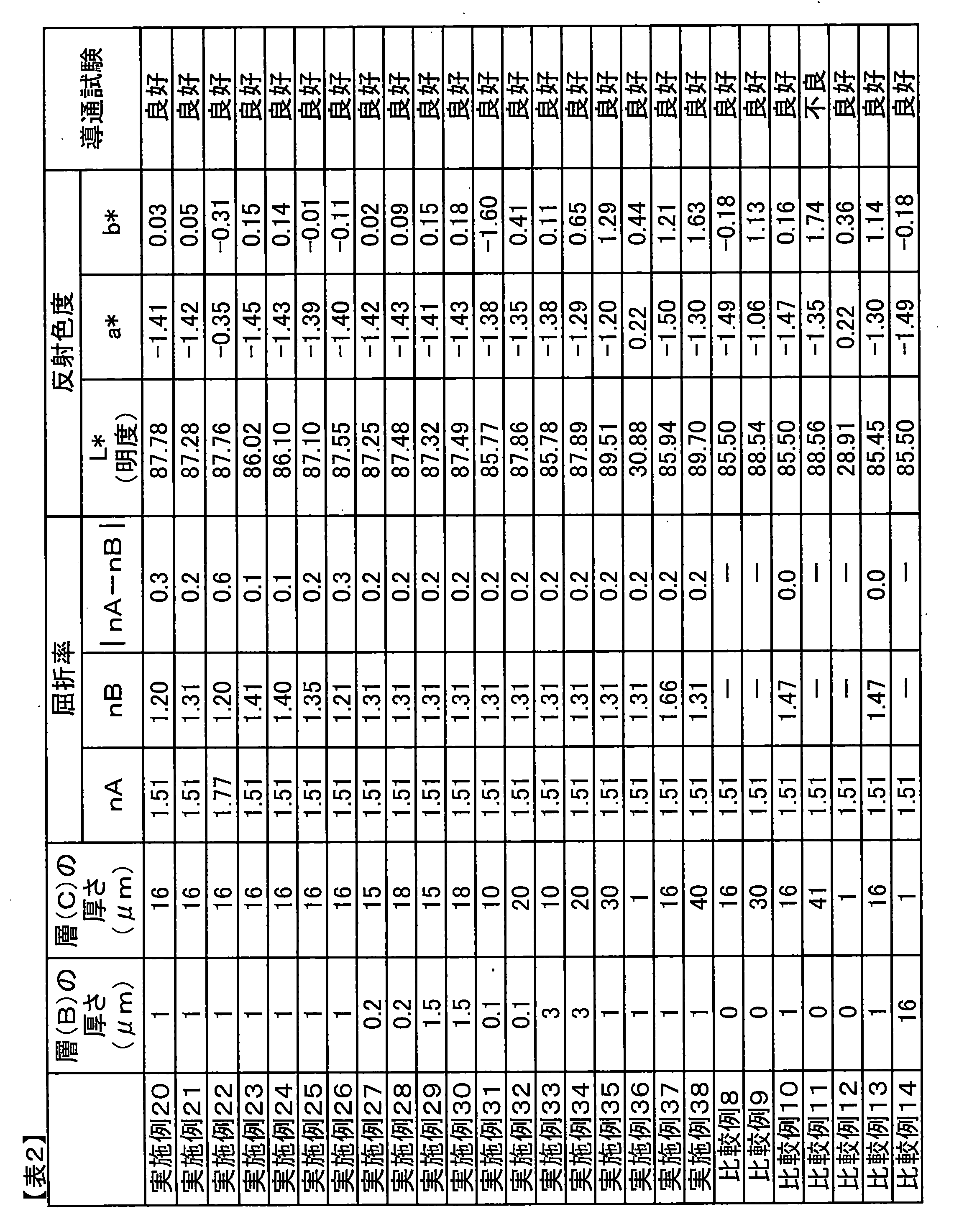

2 ・・・層(B)
3 ・・・層(C)
4 ・・・層(D)
5 ・・・ITO電極
6 ・・・透明絶縁膜
7 ・・・MAM配線
Claims (11)
- 基材(A)の表面に、層(B)、層(C)、の順で積層がされており、前記基材(A)の屈折率nAと、前記層(B)の屈折率nBとが、
0.6 ≧ | nA - nB | ≧ 0.1
の関係を満たし、前記層(C)が、顔料を含有する、積層基材。 - 前記層(B)の屈折率nBが、1.20~1.40である、請求項1記載の積層基材。
- 前記層(B)の厚さが、0.1~50μmであり、かつ、前記層(C)の厚さが、1~40μmである、請求項1又は2記載の積層基材。
- 前記層(B)が、二酸化ケイ素を含有する、請求項1~3のいずれか一項記載の積層基材。
- 前記層(B)が、ポリシロキサン及び/又はアクリル樹脂を含有する、請求項1~4のいずれか一項記載の積層基材。
- 前記層(B)が、フッ素原子をその構造中に有する化合物を含有する、請求項1~5のいずれか一項記載の積層基材。
- 前記顔料が、白色顔料である、請求項1~6のいずれか一項記載の積層基材。
- 前記層(C)が、ポリシロキサン及び/又はアクリル樹脂を含有する、請求項1~7のいずれか一項記載の積層基材。
- 請求項1~8のいずれか一項記載の積層基材を備える、カバーガラス。
- 請求項1~8のいずれか一項記載の積層基材を備える、タッチパネル。
- 請求項1~8のいずれか一項記載の積層基材を製造する方法であって、感光性樹脂組成物を用いて前記層(B)を形成する、フォトリソ工程を備える、積層基材の製造方法。
Priority Applications (4)
| Application Number | Priority Date | Filing Date | Title |
|---|---|---|---|
| US15/542,529 US10877607B2 (en) | 2015-01-19 | 2016-01-12 | Laminated base material, cover glass, touch panel, and method for manufacturing laminated base material |
| CN201680005542.5A CN107107542B (zh) | 2015-01-19 | 2016-01-12 | 层叠基材、玻璃盖板、触控面板和层叠基材的制造方法 |
| JP2016502541A JP6409862B2 (ja) | 2015-01-19 | 2016-01-12 | 積層基材、カバーガラス、タッチパネル及び積層基材の製造方法 |
| KR1020177019975A KR102542864B1 (ko) | 2015-01-19 | 2016-01-12 | 적층 기재, 커버글라스, 터치패널 및 적층 기재의 제조 방법 |
Applications Claiming Priority (2)
| Application Number | Priority Date | Filing Date | Title |
|---|---|---|---|
| JP2015007472 | 2015-01-19 | ||
| JP2015-007472 | 2015-01-19 |
Publications (1)
| Publication Number | Publication Date |
|---|---|
| WO2016117407A1 true WO2016117407A1 (ja) | 2016-07-28 |
Family
ID=56416954
Family Applications (1)
| Application Number | Title | Priority Date | Filing Date |
|---|---|---|---|
| PCT/JP2016/050642 Ceased WO2016117407A1 (ja) | 2015-01-19 | 2016-01-12 | 積層基材、カバーガラス、タッチパネル及び積層基材の製造方法 |
Country Status (6)
| Country | Link |
|---|---|
| US (1) | US10877607B2 (ja) |
| JP (1) | JP6409862B2 (ja) |
| KR (1) | KR102542864B1 (ja) |
| CN (1) | CN107107542B (ja) |
| TW (1) | TWI680877B (ja) |
| WO (1) | WO2016117407A1 (ja) |
Families Citing this family (3)
| Publication number | Priority date | Publication date | Assignee | Title |
|---|---|---|---|---|
| US11426818B2 (en) | 2018-08-10 | 2022-08-30 | The Research Foundation for the State University | Additive manufacturing processes and additively manufactured products |
| US11650705B2 (en) * | 2020-12-07 | 2023-05-16 | Tpk Advanced Solutions Inc. | Touch panel, electronic device and manufacture method thereof |
| KR102645392B1 (ko) * | 2021-07-28 | 2024-03-11 | 한국다이요잉크 주식회사 | 전자기기의 제조를 위한 곡면 커버 부재의 제조방법 |
Citations (4)
| Publication number | Priority date | Publication date | Assignee | Title |
|---|---|---|---|---|
| JP2008188996A (ja) * | 2008-03-13 | 2008-08-21 | Pilot Ink Co Ltd | 変色性積層体 |
| JP2013254116A (ja) * | 2012-06-07 | 2013-12-19 | Dainippon Printing Co Ltd | 光学積層体、及びこれを用いた偏光板 |
| JP2015118280A (ja) * | 2013-12-18 | 2015-06-25 | 大日本印刷株式会社 | 光学積層体 |
| JP2016009304A (ja) * | 2014-06-24 | 2016-01-18 | 大日本印刷株式会社 | 画像表示パネル用保護板及び画像表示装置 |
Family Cites Families (25)
| Publication number | Priority date | Publication date | Assignee | Title |
|---|---|---|---|---|
| EP0596531B1 (en) * | 1992-11-06 | 1997-07-09 | Kabushiki Kaisha Toshiba | Antireflection film and display apparatus comprising the same |
| US5932309A (en) * | 1995-09-28 | 1999-08-03 | Alliedsignal Inc. | Colored articles and compositions and methods for their fabrication |
| WO2006009296A1 (en) * | 2004-07-20 | 2006-01-26 | Fujifilm Corporation | Antireflection film, polarizing plate and image display utilizing the same |
| US8057907B2 (en) * | 2006-03-06 | 2011-11-15 | Fujifilm Corporation | Optical film, coating composition, polarizing plate and image display device |
| US7709092B2 (en) * | 2007-01-19 | 2010-05-04 | 3M Innovative Properties Company | Solar control multilayer film |
| JP4506785B2 (ja) * | 2007-06-14 | 2010-07-21 | エプソンイメージングデバイス株式会社 | 静電容量型入力装置 |
| CN101518971B (zh) * | 2008-02-29 | 2012-07-18 | E.I.内穆尔杜邦公司 | 聚酯叠层膜和使用该叠层膜的太阳能电池板 |
| WO2009116363A1 (ja) * | 2008-03-21 | 2009-09-24 | 株式会社 きもと | 光学用フィルム、積層体及びタッチパネル |
| CN102300910B (zh) * | 2008-11-28 | 2014-05-07 | 木本股份有限公司 | 具有被膜的片材及其制造方法 |
| ES2547416T3 (es) * | 2009-03-11 | 2015-10-06 | Asahi Kasei E-Materials Corporation | Composición de recubrimiento, película de recubrimiento, laminado y procedimiento para la producción del laminado |
| TW201108259A (en) * | 2009-08-18 | 2011-03-01 | Efun Technology Co Ltd | Film with color homogeneity |
| JP5810504B2 (ja) * | 2010-10-18 | 2015-11-11 | Jnc株式会社 | 積層体およびその製造方法 |
| EP2638453A4 (en) * | 2010-11-09 | 2015-11-25 | Tpk Touch Solutions Inc | Touch panel device |
| EP2684926A1 (en) * | 2011-03-09 | 2014-01-15 | Nitto Denko Corporation | Shatterproofing member with hardenable pressure-sensitive adhesive layer |
| EP2696978B1 (en) * | 2011-04-15 | 2018-12-05 | ExxonMobil Chemical Patents Inc. | Synthesis and use of m41s family molecular sieves |
| JP5110226B1 (ja) * | 2011-06-22 | 2012-12-26 | 東レフィルム加工株式会社 | 透明導電性フィルムおよびタッチパネル |
| JP2013008272A (ja) | 2011-06-27 | 2013-01-10 | Toppan Printing Co Ltd | 加飾透明保護基板一体型タッチパネルおよびその製造方法 |
| EP2808710A4 (en) * | 2012-01-25 | 2016-04-06 | Konica Minolta Advanced Layers | OPTICAL FILM |
| JP6016051B2 (ja) | 2012-01-25 | 2016-10-26 | 大日本印刷株式会社 | 表示装置用前面保護板、及び表示装置 |
| JP2013161203A (ja) * | 2012-02-03 | 2013-08-19 | Toppan Printing Co Ltd | タッチパネルセンサー基板およびそれを備える表示装置 |
| JP5887314B2 (ja) | 2012-09-19 | 2016-03-16 | 富士フイルム株式会社 | 静電容量型入力装置の製造方法および静電容量型入力装置、並びに、これを備えた画像表示装置 |
| TW201447668A (zh) * | 2013-06-14 | 2014-12-16 | Wintek Corp | 裝飾蓋板及其觸控面板 |
| JP6393179B2 (ja) * | 2014-12-16 | 2018-09-19 | 富士フイルム株式会社 | 硬化性組成物、画像表示装置の前面板、前面板一体型センサー、画像表示装置および画像表示装置の前面板の製造方法。 |
| JP2016153845A (ja) * | 2015-02-20 | 2016-08-25 | 大日本印刷株式会社 | 表示装置用前面板およびそれを備えた表示装置 |
| JP2016156890A (ja) * | 2015-02-23 | 2016-09-01 | 大日本印刷株式会社 | カラーフィルタおよび表示装置 |
-
2016
- 2016-01-12 KR KR1020177019975A patent/KR102542864B1/ko active Active
- 2016-01-12 WO PCT/JP2016/050642 patent/WO2016117407A1/ja not_active Ceased
- 2016-01-12 US US15/542,529 patent/US10877607B2/en not_active Expired - Fee Related
- 2016-01-12 JP JP2016502541A patent/JP6409862B2/ja not_active Expired - Fee Related
- 2016-01-12 CN CN201680005542.5A patent/CN107107542B/zh active Active
- 2016-01-18 TW TW105101371A patent/TWI680877B/zh active
Patent Citations (4)
| Publication number | Priority date | Publication date | Assignee | Title |
|---|---|---|---|---|
| JP2008188996A (ja) * | 2008-03-13 | 2008-08-21 | Pilot Ink Co Ltd | 変色性積層体 |
| JP2013254116A (ja) * | 2012-06-07 | 2013-12-19 | Dainippon Printing Co Ltd | 光学積層体、及びこれを用いた偏光板 |
| JP2015118280A (ja) * | 2013-12-18 | 2015-06-25 | 大日本印刷株式会社 | 光学積層体 |
| JP2016009304A (ja) * | 2014-06-24 | 2016-01-18 | 大日本印刷株式会社 | 画像表示パネル用保護板及び画像表示装置 |
Also Published As
| Publication number | Publication date |
|---|---|
| KR102542864B1 (ko) | 2023-06-14 |
| KR20170105519A (ko) | 2017-09-19 |
| JP6409862B2 (ja) | 2018-10-24 |
| US20180264778A1 (en) | 2018-09-20 |
| TW201639699A (zh) | 2016-11-16 |
| CN107107542A (zh) | 2017-08-29 |
| JPWO2016117407A1 (ja) | 2017-11-02 |
| US10877607B2 (en) | 2020-12-29 |
| TWI680877B (zh) | 2020-01-01 |
| CN107107542B (zh) | 2020-07-24 |
Similar Documents
| Publication | Publication Date | Title |
|---|---|---|
| JP6635497B2 (ja) | タッチパネル用ネガ型感光性白色組成物、タッチパネル及びタッチパネルの製造方法 | |
| CN107109131B (zh) | 触摸面板电极保护膜形成用组合物及其应用 | |
| TWI659268B (zh) | Transfer film for touch panel | |
| CN104737240B (zh) | 含有导电性纤维的层叠体、感光性导电膜及它们的应用 | |
| JP6284913B2 (ja) | タッチパネル電極保護膜形成用組成物、転写フィルム、積層体、タッチパネル用電極の保護膜及びその形成方法、静電容量型入力装置、並びに、画像表示装置 | |
| CN107250958B (zh) | 转印薄膜、静电电容型输入装置及其电极用保护膜、层叠体及其制造方法 | |
| JP5857013B2 (ja) | 加飾材付き基材およびその製造方法、タッチパネルならびに情報表示装置 | |
| JP6639098B2 (ja) | タッチパネル部材、タッチパネル及びタッチパネル表示装置 | |
| WO2017038278A1 (ja) | 転写フィルム、静電容量型入力装置の電極保護膜、積層体、積層体の製造方法および静電容量型入力装置 | |
| CN108698370B (zh) | 转印薄膜、静电电容型输入装置的电极保护膜、层叠体及静电电容型输入装置 | |
| JP2017202631A (ja) | 転写フィルム、積層基材、カバーガラス、積層基材の製造方法 | |
| JP6409862B2 (ja) | 積層基材、カバーガラス、タッチパネル及び積層基材の製造方法 | |
| JP7119390B2 (ja) | ネガ型感光性樹脂組成物およびそれを用いた硬化膜 | |
| CN107249872A (zh) | 转印薄膜、透明层叠体、静电电容型输入装置及图像显示装置 | |
| JP6313255B2 (ja) | タッチパネル部材、タッチパネル及びタッチパネル表示装置 | |
| JP2016200615A (ja) | 積層パターンの製造方法、積層パターン形成基板及びタッチパネル | |
| TWI761310B (zh) | 轉印膜、靜電電容型輸入裝置的電極保護膜、積層體及靜電電容型輸入裝置 | |
| TW201718248A (zh) | 轉印型感光性折射率調整膜 | |
| JP2016034722A (ja) | 転写フィルム、透明積層体および静電容量型入力装置 | |
| TW202239606A (zh) | 積層體及其製造方法 | |
| TW202209078A (zh) | 積層體的製造方法及觸控面板感測器 |
Legal Events
| Date | Code | Title | Description |
|---|---|---|---|
| ENP | Entry into the national phase |
Ref document number: 2016502541 Country of ref document: JP Kind code of ref document: A |
|
| 121 | Ep: the epo has been informed by wipo that ep was designated in this application |
Ref document number: 16740014 Country of ref document: EP Kind code of ref document: A1 |
|
| WWE | Wipo information: entry into national phase |
Ref document number: 15542529 Country of ref document: US |
|
| ENP | Entry into the national phase |
Ref document number: 20177019975 Country of ref document: KR Kind code of ref document: A |
|
| NENP | Non-entry into the national phase |
Ref country code: DE |
|
| 122 | Ep: pct application non-entry in european phase |
Ref document number: 16740014 Country of ref document: EP Kind code of ref document: A1 |