WO2016117287A1 - 貼り合わせsoiウェーハの製造方法 - Google Patents
貼り合わせsoiウェーハの製造方法 Download PDFInfo
- Publication number
- WO2016117287A1 WO2016117287A1 PCT/JP2016/000051 JP2016000051W WO2016117287A1 WO 2016117287 A1 WO2016117287 A1 WO 2016117287A1 JP 2016000051 W JP2016000051 W JP 2016000051W WO 2016117287 A1 WO2016117287 A1 WO 2016117287A1
- Authority
- WO
- WIPO (PCT)
- Prior art keywords
- polishing
- wafer
- polycrystalline silicon
- silicon layer
- bonding
- Prior art date
- Legal status (The legal status is an assumption and is not a legal conclusion. Google has not performed a legal analysis and makes no representation as to the accuracy of the status listed.)
- Ceased
Links
Images

Classifications
-
- H—ELECTRICITY
- H10—SEMICONDUCTOR DEVICES; ELECTRIC SOLID-STATE DEVICES NOT OTHERWISE PROVIDED FOR
- H10P—GENERIC PROCESSES OR APPARATUS FOR THE MANUFACTURE OR TREATMENT OF DEVICES COVERED BY CLASS H10
- H10P90/00—Preparation of wafers not covered by a single main group of this subclass, e.g. wafer reinforcement
- H10P90/19—Preparing inhomogeneous wafers
- H10P90/1904—Preparing vertically inhomogeneous wafers
- H10P90/1906—Preparing SOI wafers
- H10P90/1914—Preparing SOI wafers using bonding
- H10P90/1916—Preparing SOI wafers using bonding with separation or delamination along an ion implanted layer, e.g. Smart-cut
-
- H—ELECTRICITY
- H10—SEMICONDUCTOR DEVICES; ELECTRIC SOLID-STATE DEVICES NOT OTHERWISE PROVIDED FOR
- H10P—GENERIC PROCESSES OR APPARATUS FOR THE MANUFACTURE OR TREATMENT OF DEVICES COVERED BY CLASS H10
- H10P52/00—Grinding, lapping or polishing of wafers, substrates or parts of devices
-
- H—ELECTRICITY
- H10—SEMICONDUCTOR DEVICES; ELECTRIC SOLID-STATE DEVICES NOT OTHERWISE PROVIDED FOR
- H10D—INORGANIC ELECTRIC SEMICONDUCTOR DEVICES
- H10D62/00—Semiconductor bodies, or regions thereof, of devices having potential barriers
- H10D62/80—Semiconductor bodies, or regions thereof, of devices having potential barriers characterised by the materials
- H10D62/83—Semiconductor bodies, or regions thereof, of devices having potential barriers characterised by the materials being Group IV materials, e.g. B-doped Si or undoped Ge
- H10D62/832—Semiconductor bodies, or regions thereof, of devices having potential barriers characterised by the materials being Group IV materials, e.g. B-doped Si or undoped Ge being Group IV materials comprising two or more elements, e.g. SiGe
- H10D62/8325—Silicon carbide
-
- H—ELECTRICITY
- H10—SEMICONDUCTOR DEVICES; ELECTRIC SOLID-STATE DEVICES NOT OTHERWISE PROVIDED FOR
- H10D—INORGANIC ELECTRIC SEMICONDUCTOR DEVICES
- H10D86/00—Integrated devices formed in or on insulating or conducting substrates, e.g. formed in silicon-on-insulator [SOI] substrates or on stainless steel or glass substrates
-
- H—ELECTRICITY
- H10—SEMICONDUCTOR DEVICES; ELECTRIC SOLID-STATE DEVICES NOT OTHERWISE PROVIDED FOR
- H10D—INORGANIC ELECTRIC SEMICONDUCTOR DEVICES
- H10D86/00—Integrated devices formed in or on insulating or conducting substrates, e.g. formed in silicon-on-insulator [SOI] substrates or on stainless steel or glass substrates
- H10D86/201—Integrated devices formed in or on insulating or conducting substrates, e.g. formed in silicon-on-insulator [SOI] substrates or on stainless steel or glass substrates the substrates comprising an insulating layer on a semiconductor body, e.g. SOI
-
- H—ELECTRICITY
- H10—SEMICONDUCTOR DEVICES; ELECTRIC SOLID-STATE DEVICES NOT OTHERWISE PROVIDED FOR
- H10P—GENERIC PROCESSES OR APPARATUS FOR THE MANUFACTURE OR TREATMENT OF DEVICES COVERED BY CLASS H10
- H10P14/00—Formation of materials, e.g. in the shape of layers or pillars
-
- H—ELECTRICITY
- H10—SEMICONDUCTOR DEVICES; ELECTRIC SOLID-STATE DEVICES NOT OTHERWISE PROVIDED FOR
- H10P—GENERIC PROCESSES OR APPARATUS FOR THE MANUFACTURE OR TREATMENT OF DEVICES COVERED BY CLASS H10
- H10P14/00—Formation of materials, e.g. in the shape of layers or pillars
- H10P14/20—Formation of materials, e.g. in the shape of layers or pillars of semiconductor materials
- H10P14/32—Formation of materials, e.g. in the shape of layers or pillars of semiconductor materials characterised by intermediate layers between substrates and deposited layers
- H10P14/3242—Structure
- H10P14/3244—Layer structure
- H10P14/3246—Monolayers
-
- H—ELECTRICITY
- H10—SEMICONDUCTOR DEVICES; ELECTRIC SOLID-STATE DEVICES NOT OTHERWISE PROVIDED FOR
- H10P—GENERIC PROCESSES OR APPARATUS FOR THE MANUFACTURE OR TREATMENT OF DEVICES COVERED BY CLASS H10
- H10P14/00—Formation of materials, e.g. in the shape of layers or pillars
- H10P14/20—Formation of materials, e.g. in the shape of layers or pillars of semiconductor materials
- H10P14/34—Deposited materials, e.g. layers
- H10P14/3451—Structure
- H10P14/3452—Microstructure
- H10P14/3456—Polycrystalline
-
- H—ELECTRICITY
- H10—SEMICONDUCTOR DEVICES; ELECTRIC SOLID-STATE DEVICES NOT OTHERWISE PROVIDED FOR
- H10P—GENERIC PROCESSES OR APPARATUS FOR THE MANUFACTURE OR TREATMENT OF DEVICES COVERED BY CLASS H10
- H10P14/00—Formation of materials, e.g. in the shape of layers or pillars
- H10P14/60—Formation of materials, e.g. in the shape of layers or pillars of insulating materials
-
- H—ELECTRICITY
- H10—SEMICONDUCTOR DEVICES; ELECTRIC SOLID-STATE DEVICES NOT OTHERWISE PROVIDED FOR
- H10P—GENERIC PROCESSES OR APPARATUS FOR THE MANUFACTURE OR TREATMENT OF DEVICES COVERED BY CLASS H10
- H10P90/00—Preparation of wafers not covered by a single main group of this subclass, e.g. wafer reinforcement
- H10P90/12—Preparing bulk and homogeneous wafers
-
- H—ELECTRICITY
- H10—SEMICONDUCTOR DEVICES; ELECTRIC SOLID-STATE DEVICES NOT OTHERWISE PROVIDED FOR
- H10P—GENERIC PROCESSES OR APPARATUS FOR THE MANUFACTURE OR TREATMENT OF DEVICES COVERED BY CLASS H10
- H10P90/00—Preparation of wafers not covered by a single main group of this subclass, e.g. wafer reinforcement
- H10P90/12—Preparing bulk and homogeneous wafers
- H10P90/123—Preparing bulk and homogeneous wafers by grinding or lapping
-
- H—ELECTRICITY
- H10—SEMICONDUCTOR DEVICES; ELECTRIC SOLID-STATE DEVICES NOT OTHERWISE PROVIDED FOR
- H10P—GENERIC PROCESSES OR APPARATUS FOR THE MANUFACTURE OR TREATMENT OF DEVICES COVERED BY CLASS H10
- H10P90/00—Preparation of wafers not covered by a single main group of this subclass, e.g. wafer reinforcement
- H10P90/12—Preparing bulk and homogeneous wafers
- H10P90/126—Preparing bulk and homogeneous wafers by chemical etching
-
- H—ELECTRICITY
- H10—SEMICONDUCTOR DEVICES; ELECTRIC SOLID-STATE DEVICES NOT OTHERWISE PROVIDED FOR
- H10P—GENERIC PROCESSES OR APPARATUS FOR THE MANUFACTURE OR TREATMENT OF DEVICES COVERED BY CLASS H10
- H10P95/00—Generic processes or apparatus for manufacture or treatments not covered by the other groups of this subclass
-
- H—ELECTRICITY
- H10—SEMICONDUCTOR DEVICES; ELECTRIC SOLID-STATE DEVICES NOT OTHERWISE PROVIDED FOR
- H10W—GENERIC PACKAGES, INTERCONNECTIONS, CONNECTORS OR OTHER CONSTRUCTIONAL DETAILS OF DEVICES COVERED BY CLASS H10
- H10W10/00—Isolation regions in semiconductor bodies between components of integrated devices
- H10W10/10—Isolation regions comprising dielectric materials
- H10W10/181—Semiconductor-on-insulator [SOI] isolation regions, e.g. buried oxide regions of SOI wafers
-
- H—ELECTRICITY
- H10—SEMICONDUCTOR DEVICES; ELECTRIC SOLID-STATE DEVICES NOT OTHERWISE PROVIDED FOR
- H10P—GENERIC PROCESSES OR APPARATUS FOR THE MANUFACTURE OR TREATMENT OF DEVICES COVERED BY CLASS H10
- H10P52/00—Grinding, lapping or polishing of wafers, substrates or parts of devices
- H10P52/40—Chemomechanical polishing [CMP]
- H10P52/403—Chemomechanical polishing [CMP] of conductive or resistive materials
-
- H—ELECTRICITY
- H10—SEMICONDUCTOR DEVICES; ELECTRIC SOLID-STATE DEVICES NOT OTHERWISE PROVIDED FOR
- H10P—GENERIC PROCESSES OR APPARATUS FOR THE MANUFACTURE OR TREATMENT OF DEVICES COVERED BY CLASS H10
- H10P90/00—Preparation of wafers not covered by a single main group of this subclass, e.g. wafer reinforcement
- H10P90/12—Preparing bulk and homogeneous wafers
- H10P90/129—Preparing bulk and homogeneous wafers by polishing
Definitions
- the present invention relates to a method for manufacturing a bonded SOI wafer.
- the substrate needs to be an insulator.
- BOX layer buried oxide film
- the oxide film has poor thermal conductivity, and heat generated when operating a high-frequency device cannot be removed. It becomes a problem. Therefore, a method of using a high-resistance Si substrate as a support substrate for the SOI wafer has been considered. Thereby, conduction of electricity below the BOX layer can be suppressed, and harmonics of the high-frequency device can be suppressed.
- the most common layer for trapping carriers is a polycrystalline silicon layer.
- the polycrystalline silicon layer traps carriers at the grain boundaries and suppresses electrical conduction.
- a polycrystalline silicon layer is laminated on a support substrate wafer (base wafer), and this is bonded to a wafer with an oxide film (bond wafer).
- An underlying SOI wafer can be produced.
- the surface of the polycrystalline silicon layer needs to be smooth, and a method of bonding by removing the surface roughness using polishing has been considered.
- a silicon single crystal ingot is grown by the Czochralski method, and this ingot is sliced. After being processed into a thin disc shape, it is finished into a mirror-like wafer (mirror wafer) through various processes such as chamfering, lapping, etching, and polishing.
- polishing is usually performed through a plurality of stages from rough polishing to final polishing. For example, after the lapping process or the etching process, primary polishing is performed with a polishing allowance of about several ⁇ m in order to remove distortion on the wafer surface and flatten it. Next, in order to remove scratches and the like generated in the primary polishing and improve the surface roughness, secondary polishing is performed with a polishing margin of about 1 ⁇ m. Further, in order to obtain a haze-free surface, finish polishing is performed with a polishing allowance of less than 1 ⁇ m. Thus, the surface of the wafer is mirror-finished through rough polishing (primary polishing and secondary polishing) and finish polishing (see, for example, paragraph (0004) of Patent Document 4).
- polishing is performed by setting conditions so that the roughness or the like becomes a low value (for example, refer to paragraph (0027) of Patent Document 5).
- a method of trapping a carrier trapping layer immediately below the BOX layer of the SOI wafer is adopted, and a polycrystalline silicon layer is used as the carrier trapping layer.
- the surface of the polycrystalline silicon layer on the base wafer needs to be smooth, and polishing is used to reduce the surface roughness of the polycrystalline silicon layer on the base wafer. A method of removing and bonding is considered.
- the surface roughness of the base wafer does not necessarily require the surface roughness necessary for device fabrication (surface roughness equivalent to PW used for device fabrication). It is possible to stack a polycrystalline silicon layer on a substrate having a surface as rough as a chemical etching surface (hereinafter referred to as CW surface).
- the surface of the polycrystalline silicon layer laminated on the CW surface reflects the surface roughness and waviness of the CW surface, and in order to obtain a smooth surface that can be bonded, In this polishing, measures such as extremely increasing the polishing allowance are required, which is a problem.
- the present invention has been made in view of the above-described problems, and is provided with a minimum polishing step necessary to obtain a smooth polycrystalline silicon surface after polishing so that generation of voids after bonding can be suppressed.
- An object of the present invention is to provide a method for manufacturing a laminated SOI wafer.
- the present invention is a method for manufacturing a bonded SOI wafer by bonding a bond wafer made of silicon single crystal and a base wafer together through an insulating film.
- a chemical etching surface wafer is used as the base wafer, and the chemical etching is performed.
- the surface of the polycrystalline silicon layer is applied to the surface of the polycrystalline silicon layer.
- a bonded SOI wafer manufacturing method characterized by performing secondary polishing, or secondary polishing and finish polishing.
- the polishing step in the production of the wafer can be a minimum polishing step necessary to obtain a smooth polycrystalline silicon surface after polishing that can suppress the generation of voids after bonding.
- the base wafer having a resistivity of 100 ⁇ ⁇ cm or more it is preferable to use the base wafer having a resistivity of 100 ⁇ ⁇ cm or more. If such a base wafer is used, an SOI wafer suitable as a substrate for a high-frequency device can be manufactured.
- the primary polishing is preferably performed by double-side polishing.
- Double-side polishing can be suitably used as the primary polishing before growing the polycrystalline silicon layer of the base wafer.
- the polishing step in manufacturing the bonded SOI wafer is performed after polishing a smooth polycrystalline silicon surface that can suppress the generation of voids after bonding. It is possible to make the polishing process the minimum necessary to obtain. Therefore, a high-quality bonded SOI wafer can be obtained with high productivity at low cost.
- the inventors set the polishing step in the production of the bonded SOI wafer as the minimum polishing step necessary for obtaining a smooth polycrystalline silicon surface after polishing that can suppress the generation of voids after bonding.
- the present inventors have made extensive studies on a method for manufacturing a bonded SOI wafer that can be bonded. As a result, in the step of depositing the polycrystalline silicon layer, after the primary polishing is performed on the chemically etched surface, the polycrystalline silicon layer is deposited on the surface subjected to the primary polishing, and the surface of the polycrystalline silicon layer is polished.
- the polishing process in the production of the bonded SOI wafer can be smooth so as to suppress the generation of voids after bonding.
- the inventors have found that the minimum necessary polishing step for obtaining a polycrystalline silicon surface after polishing can be achieved.
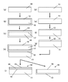
- a base wafer having a chemically etched surface is prepared (see step S11 in FIG. 1). Specifically, for example, a silicon single crystal ingot is sliced, and lapping, laser mark printing, and chemical etching are performed to prepare a base wafer 11 having a chemical etching surface (see FIG. 2D).
- step S12 in FIG. 1 primary polishing is performed on the chemically etched surface of the base wafer (see step S12 in FIG. 1). Specifically, for example, primary polishing is performed on at least one chemical etching surface of the base wafer 11 (at least the upper surface of the base wafer 11 in FIG. 2), and mirror chamfering is performed (FIG. 2 (e)). See). In this state, the surface roughness of the surface of the base wafer 11 is about 0.3 nm as an RMS value of AFM measurement (1 ⁇ m square).
- a polycrystalline silicon layer is deposited on the surface of the base wafer subjected to the primary polishing (see step S13 in FIG. 1).
- the polycrystalline silicon layer 12 is deposited on the surface of the base wafer 11 where the primary polishing has been performed (the upper surface of the base wafer 11 in FIG. 2E) (see FIG. 2F).
- the polycrystalline silicon layer 12 is generally formed by a CVD apparatus.
- CVD apparatus there is an epireactor for the purpose of laminating a single crystal silicon layer, but in this apparatus as well, it is not a single crystal by selecting conditions such as lowering the deposition temperature. It is possible to stack silicon.
- the surface roughness after stacking the polycrystalline silicon layers is about 15 nm as an RMS value of AFM measurement (1 ⁇ m square).
- secondary polishing, or secondary polishing and finish polishing are performed on the surface of the polycrystalline silicon layer of the base wafer (see step S14 in FIG. 1).
- the surface of the polycrystalline silicon layer 12 of the base wafer 11 is subjected to secondary polishing with an allowance of about 0.5 to 1 ⁇ m, and if necessary, with an allowance less than the secondary polish.
- a surface roughness of about 0.15 nm can be obtained with an RMS value of AFM measurement (1 ⁇ m square) (see FIG. 2G).
- an insulating film is formed on the bonding surface of the bond wafer (see step S15 in FIG. 1).
- a silicon single crystal wafer is prepared as the bond wafer 10 (see FIG. 2A), and a buried oxide film layer (BOX layer, insulating film) 16 (see FIG. 2I).
- Oxide film growth for example, thermal oxidation treatment
- oxide film growth for example, thermal oxidation treatment
- hydrogen ions or rare gas ions can be implanted from above the oxide film 13 by an ion implanter to form the ion implantation layer 17 (see FIG. 2C).
- the ion implantation acceleration voltage is selected so that the target thickness of the peeled silicon layer (that is, the SOI layer 15 (see FIG. 2I)) can be obtained.
- the polished surface of the polycrystalline silicon layer of the base wafer is bonded to the bond wafer through the insulating layer (see step S16 in FIG. 1). Specifically, for example, ion implantation is performed on the base wafer 11 on which the polycrystalline silicon layer 12 is formed so that the surface of the base wafer 11 on which the polycrystalline silicon layer 12 is formed and the implantation surface of the bond wafer 10 are in contact with each other. The bonded wafer 10 on which the layer 17 is formed is adhered and bonded together (see FIG. 2H).
- the bonded bond wafer is thinned to form an SOI layer (see step S17 in FIG. 1). Specifically, for example, a heat treatment (exfoliation heat treatment) for generating a microbubble layer on the ion implantation layer 17 is performed on the bonded wafer, and the generated microbubble layer is peeled off to be embedded on the base wafer 11.
- a bonded wafer 14 on which the layer 16 and the SOI layer 15 are formed is manufactured (see FIG. 2I). At this time, the release wafer 18 having the release surface 19 is derived.
- the polycrystalline silicon layer is formed on the surface subjected to the primary polishing without performing the secondary polishing and the final polishing.
- the step of depositing and polishing the surface of the polycrystalline silicon layer the surface of the polycrystalline silicon layer is bonded to the surface by performing secondary polishing or secondary polishing and finish polishing without performing primary polishing.
- the polishing process in the manufacture of SOI wafers can be made the minimum polishing process necessary for obtaining a smooth polycrystalline silicon surface after polishing so that the generation of voids after bonding can be suppressed. .
- a base wafer 11 having a resistivity of 100 ⁇ ⁇ cm or more it is preferable to use a base wafer 11 having a resistivity of 100 ⁇ ⁇ cm or more. If such a base wafer is used, an SOI wafer suitable as a substrate for a high-frequency device can be manufactured.
- S11 to S14 and S15 in FIG. 1 and (a) to (c) and (d) to (g) in FIG. 2 may be performed either first or simultaneously. Needless to say, it is good.
- the primary polishing is preferably performed by double-side polishing. Double-side polishing can be suitably used as the primary polishing before growing the polycrystalline silicon layer of the base wafer.
- a bond wafer As a bond wafer, a CZ silicon single crystal wafer (PW: mirror polished wafer) having a diameter of 300 mm, p-type, 10 ⁇ ⁇ cm, crystal orientation ⁇ 100> and having no COP (Crystal Oriented Particle) is prepared, and a 200 nm oxide film is heated. After growing by oxidation, H + ions were implanted at 6 ⁇ 10 16 atoms / cm 2 with an acceleration energy of 70 keV using an ion implanter.
- PW mirror polished wafer
- the base wafer is sliced from a CZ silicon single crystal having an oxygen concentration of 9.6 ppma (ASTM'79) and a resistivity of 5200 ⁇ ⁇ cm, followed by lapping and peripheral grinding, back laser mark marking process, and chemical etching.
- the produced CW wafer was subjected to primary polishing with a double-side polishing machine, and the outer peripheral portion was subjected to mirror chamfering polishing. At this time, the surface roughness of the wafer surface was about 0.3 nm as the RMS value of AFM measurement (1 ⁇ m square). After the polycrystalline silicon layer was laminated on the primary polished surface at a temperature of 900 ° C.
- an RTA treatment (planarization heat treatment) is performed at 1150 ° C. for 30 seconds in a hydrogen atmosphere, and then an oxidation heat treatment and HF cleaning are performed, whereby an SOI layer having a thickness of 150 nm and an SOI with an embedded polycrystalline silicon layer is obtained. A wafer could be obtained.
- the wafer polishing step in the manufacturing process of the embodiment is primary polishing before stacking the polycrystalline silicon layer, secondary polishing and finish polishing after stacking the polycrystalline silicon layer, and “secondary polishing + finish polishing”. Assuming that the productivity when the process is performed once is 1, the productivity in the polishing process of the bonded SOI wafer of the example is 1.
- Comparative Example 1 A bonded SOI wafer was manufactured in the same manner as in the example. However, the base wafer is sliced from CZ silicon single crystal, and lapping and outer periphery grinding, back surface laser mark engraving process, and CW wafer produced through chemical etching are subjected to primary polishing with a double-side polisher. After the part was mirror chamfered and polished, secondary polishing and finish polishing were further used. At this time, the surface roughness of the wafer surface was about 0.1 nm as the RMS value of AFM measurement (1 ⁇ m square). In Comparative Example 1, after the polycrystalline silicon layer was laminated, secondary polishing and final polishing were performed in the same manner as in the Example, and the surface roughness after the polishing was about 0.15 nm.
- the wafer polishing step in the manufacturing process of Comparative Example 1 is primary polishing, secondary polishing, and finish polishing before stacking the polycrystalline silicon layer, and secondary polishing and finish polishing after stacking the polycrystalline silicon layer. Assuming that the productivity when performing “secondary polishing + finish polishing” once is 1, the productivity of the bonded SOI wafer polishing process of Comparative Example 1 was 0.5.
- a bonded SOI wafer was manufactured in the same manner as in the example. However, the base wafer was sliced from the CZ silicon single crystal, and the primary polishing was not performed on the CW wafer manufactured through the lapping and outer periphery grinding, the back surface laser mark marking process, and the chemical etching. At this time, the surface roughness of the wafer surface was about 10 nm as the RMS value of AFM measurement (1 ⁇ m square). In Comparative Example 2, the surface roughness after polishing after lamination of the polycrystalline silicon layer was about 0.25 nm as an RMS value of AFM measurement (1 ⁇ m square).
- Comparative Example 2 since the surface roughness after polishing the polycrystalline silicon layer is large, the bonding is not sufficient, and the SOI layer is not transferred to the base wafer side after the peeling step that causes peeling in the hydrogen ion implanted layer. Many voids having a diameter of 1 mm or more were generated in the surface. In Comparative Example 2, a large number of voids were generated in the surface in the above-described peeling process, and the production of the bonded SOI wafer was stopped. Therefore, the productivity of the polishing process was not evaluated.
- Table 1 shows the steps and results of the above Examples, Comparative Example 1, and Comparative Example 2.
- the present invention is not limited to the above embodiment.
- the above-described embodiment is an exemplification, and the present invention has substantially the same configuration as the technical idea described in the claims of the present invention, and any device that exhibits the same function and effect is the present invention. It is included in the technical scope of the invention.
Landscapes
- Mechanical Treatment Of Semiconductor (AREA)
- Chemical & Material Sciences (AREA)
- Crystallography & Structural Chemistry (AREA)
- Chemical Kinetics & Catalysis (AREA)
- General Chemical & Material Sciences (AREA)
- Recrystallisation Techniques (AREA)
- Element Separation (AREA)
Abstract
本発明は、いずれもシリコン単結晶からなるボンドウェーハとベースウェーハとを絶縁膜を介して貼り合わせて貼り合わせSOIウェーハを製造する方法であって、ベースウェーハの貼り合わせ面側に多結晶シリコン層を堆積する工程と、多結晶シリコン層の表面を研磨する工程と、ボンドウェーハの貼り合わせ面に絶縁膜を形成する工程と、絶縁膜を介してベースウェーハの前記多結晶シリコン層の研磨面とボンドウェーハを貼り合わせる工程と、貼り合わせられたボンドウェーハを薄膜化してSOI層を形成する工程とを有し、多結晶シリコン層を堆積する工程において、ベースウェーハとして、ケミカルエッチング面を有するウェーハを用い、ケミカルエッチング面に1次研磨を行った後、1次研磨を行った面に多結晶シリコン層を堆積し、多結晶シリコン層の表面を研磨する工程において、多結晶シリコン層の表面に2次研磨、又は、2次研磨及び仕上げ研磨を行うことを特徴とする貼り合わせSOIウェーハの製造方法である。これにより、貼り合わせ後のボイド発生を抑制できるような平滑な多結晶シリコン面を研磨後に得るのに必要最小限な研磨工程を備えた貼り合わせSOIウェーハの製造方法が提供される。
Description
本発明は、貼り合わせSOIウェーハの製造方法に関する。
携帯端末、インターネット通信、等の発達により、無線による情報のやりとりの、情報量や通信速度への要求は、限りなく増大する一方である。近年では、RFスイッチ等の高周波デバイスとして、これまでSOS(サファイア上シリコン:Silicon On Sapphire)やGaAsの基板等により作製していた単一の素子を、Si基板上に集積化されたデバイスに置き換えて、小型化・集積化する技術が、盛んに採用されるようになった。特に、SOIウェーハを使用して高周波デバイスを作製する方法が、市場を大きく伸ばしている。
高周波デバイスの性能として、通信の混線を防止する為に、2次高調波、3次高調波の抑制が、主要な要求項目となっている。この為には、基板が絶縁体であることが必要になる。SOIウェーハにおいては、埋め込み酸化膜(BOX層)の厚さを大きくすることが一つの方法と考えられるが、酸化膜は熱伝導率が悪く、高周波デバイスを動作させる際の発熱が除去できないことが問題になる。そこで、SOIウェーハの支持基板として、高抵抗Si基板を使用する方法が考えられた。これにより、BOX層より下での電気の伝導を抑制することができて、高周波デバイスの高調波を抑制することができる。しかし、SOI層に電位がかかると、BOX層直下のSi基板表面では空乏層が発生して反転層が形成され、この部分での電気伝導が発生する為に、高調波が抑制できなくなる。この問題を解決する為に、BOX層の直下にキャリアをトラップする層を内在させる手法が取られる(例えば、特許文献1~3を参照)。
キャリアをトラップする層としては、多結晶シリコン層が最も一般的である。多結晶シリコン層は結晶粒界でキャリアをトラップし、電気伝導を抑制する。
多結晶シリコン層を内在する方法として、支持基板用ウェーハ(ベースウェーハ)に多結晶シリコン層を積層し、これを酸化膜の付いたウェーハ(ボンドウェーハ)と貼り合わせることで、多結晶シリコン層を内在したSOIウェーハを作製することができる。ただし、この際、ウェーハ貼り合わせを実現するために、多結晶シリコン層の表面は平滑である必要があり、研磨を用いて表面粗さを除去して貼り合わせを行う方法が考えられている。
多結晶シリコン層を内在する方法として、支持基板用ウェーハ(ベースウェーハ)に多結晶シリコン層を積層し、これを酸化膜の付いたウェーハ(ボンドウェーハ)と貼り合わせることで、多結晶シリコン層を内在したSOIウェーハを作製することができる。ただし、この際、ウェーハ貼り合わせを実現するために、多結晶シリコン層の表面は平滑である必要があり、研磨を用いて表面粗さを除去して貼り合わせを行う方法が考えられている。
ところで、デバイス作製等に用いられる一般的な鏡面研磨されたシリコン単結晶ウェーハ(以下、PWと称する)を製造する場合、例えばチョクラルスキー法でシリコン単結晶インゴットを育成し、このインゴットをスライスして薄い円板状に加工した後、面取り、ラッピング、エッチング、研磨等の種々の工程を経て鏡面状のウェーハ(鏡面ウェーハ)に仕上げられる。
シリコンウェーハの研磨工程では、通常、粗研磨から仕上げ研磨へと複数の段階を経て研磨が行われる。例えば、ラッピング工程あるいはエッチング工程の後、ウェーハの表面における歪みを除去し、平坦化するため、数μm程度の研磨代で1次研磨を行う。次いで、1次研磨で発生したキズ等を除去し、表面粗さを改善するため、1μm程度の研磨代で2次研磨を行う。さらに、ヘイズフリーの表面にするため、1μm未満の研磨代で仕上げ研磨を行う。このように粗研磨(1次研磨及び2次研磨)と、仕上げ研磨を経てウェーハの表面が鏡面化される(例えば、特許文献4の(0004)段落を参照)。
この研磨の回を重ねる毎に、研磨砥粒の粒度を細かくしたり、研磨布の硬度を下げる等、研磨条件を緩和させたりしながら、その段階毎に研磨される鏡面部の平坦度や面粗さ等を低い値となるように条件を設定して研磨している(例えば、特許文献5の(0027)段落を参照)。
特に直径300mmのシリコンウェーハでは厳しい平坦度の仕様を満足するために両面研磨での一次研磨を行い、その後に表面のキズや面粗さの改善のために片面での表面二次及び仕上げ研磨を行っている(例えば、特許文献6の(0002)段落を参照)。
上述したように、高周波デバイス用の基板として、SOIウェーハのBOX層の直下にキャリアをトラップする層を内在させる手法が取られるようになり、このキャリアをトラップする層としては、多結晶シリコン層が最も一般的である。ベースウェーハとボンドウェーハとの貼り合わせを実現するために、ベースウェーハ上の多結晶シリコン層の表面は平滑である必要があり、研磨を用いてベースウェーハ上の多結晶シリコン層の表面粗さを除去して貼り合わせを行う方法が考えられている。
ベースウェーハに多結晶シリコンを積層する際には、ベースウェーハの表面粗さは、必ずしもデバイス作製に必要な表面粗さ(デバイス作製に用いられるPWと同等の表面粗さ)を必要としない。ケミカルエッチング面(以下、CW面と称する)程度に表面粗さのある基板上にも、多結晶シリコン層を積層することは可能である。
しかしながら、CW面上に積層した多結晶シリコン層の表面は、CW面の面粗さやうねりを反映したものであり、貼り合わせを可能とする平滑な面を得るためには、多結晶シリコン積層後の研磨において研磨代を極端に大きくするなどの対策が必要となり、問題となる。
しかしその一方で、PW面の上に多結晶シリコン層を積層しても、多結晶シリコン層の表面粗さは、元のPW面の面粗さよりも大きく悪化し、貼り合わせを可能とする平滑な面を得るためには、多結晶シリコン層積層後の研磨を行う必要がある。
これは、PW面を得るための研磨と同様の工程となり、ベースウェーハに多結晶シリコン層を積層する前と後の両方で研磨を行う工程が重複してしまい、研磨工程の効率(生産性)を著しく落とす結果となるという問題がある。
本発明は、上記問題点に鑑みてなされたものであって、貼り合わせ後のボイド発生を抑制できるような平滑な多結晶シリコン面を研磨後に得るのに必要最小限な研磨工程を備えた貼り合わせSOIウェーハの製造方法を提供することを目的とする。
上記目的を達成するために、本発明は、いずれもシリコン単結晶からなるボンドウェーハとベースウェーハとを絶縁膜を介して貼り合わせて貼り合わせSOIウェーハを製造する方法であって、前記ベースウェーハの貼り合わせ面側に多結晶シリコン層を堆積する工程と、該多結晶シリコン層の表面を研磨する工程と、前記ボンドウェーハの貼り合わせ面に前記絶縁膜を形成する工程と、前記絶縁膜を介して前記ベースウェーハの前記多結晶シリコン層の研磨面と前記ボンドウェーハを貼り合わせる工程と、貼り合わせられた前記ボンドウェーハを薄膜化してSOI層を形成する工程とを有し、前記多結晶シリコン層を堆積する工程において、前記ベースウェーハとして、ケミカルエッチング面を有するウェーハを用い、前記ケミカルエッチング面に1次研磨を行った後、該1次研磨を行った面に前記多結晶シリコン層を堆積し、前記多結晶シリコン層の表面を研磨する工程において、前記多結晶シリコン層の表面に2次研磨、又は、2次研磨及び仕上げ研磨を行うことを特徴とする貼り合わせSOIウェーハの製造方法を提供する。
このように、多結晶シリコン層を堆積する工程において、ケミカルエッチング面に1次研磨を行った後、2次研磨、仕上げ研磨を行うことなく、1次研磨を行った面に多結晶シリコン層を堆積し、多結晶シリコン層の表面を研磨する工程において、多結晶シリコン層の表面に1次研磨を行うことなく、2次研磨、又は、2次研磨及び仕上げ研磨を行うことで、貼り合わせSOIウェーハの製造における研磨工程を、貼り合わせ後のボイド発生を抑制できるような平滑な多結晶シリコン面を研磨後に得るのに必要最小限な研磨工程とすることができる。
このとき、前記ベースウェーハとして、抵抗率が100Ω・cm以上のものを用いることが好ましい。
このようなベースウェーハを用いれば、高周波デバイス用の基板として好適なSOIウェーハを製造することができる。
このようなベースウェーハを用いれば、高周波デバイス用の基板として好適なSOIウェーハを製造することができる。
このとき、前記1次研磨を両面研磨で行うことが好ましい。
ベースウェーハの多結晶シリコン層成長前の1次研磨として、両面研磨を好適に用いることができる。
ベースウェーハの多結晶シリコン層成長前の1次研磨として、両面研磨を好適に用いることができる。
以上のように、本発明の貼り合わせSOIウェーハの製造方法によれば、貼り合わせSOIウェーハの製造における研磨工程を、貼り合わせ後のボイド発生を抑制できるような平滑な多結晶シリコン面を研磨後に得るのに必要最小限な研磨工程とすることができる。従って、低コストで高品質の貼り合わせSOIウェーハを高い生産性で得ることができる。
以下、本発明について、実施態様の一例として、図を参照しながら詳細に説明するが、本発明はこれに限定されるものではない。
前述のように、高周波デバイス用の基板として、SOIウェーハのBOX層の直下にキャリアをトラップする層として多結晶シリコン層を内在させる手法が取られるようになってきている。このようなSOIウェーハの製造において、ベースウェーハとボンドウェーハとの貼り合わせを実現するために、ベースウェーハ上の多結晶シリコン層の表面は平滑である必要があり、研磨を用いてベースウェーハ上の多結晶シリコン層の表面粗さを除去して貼り合わせを行う方法が考えられている。
前述のように、高周波デバイス用の基板として、SOIウェーハのBOX層の直下にキャリアをトラップする層として多結晶シリコン層を内在させる手法が取られるようになってきている。このようなSOIウェーハの製造において、ベースウェーハとボンドウェーハとの貼り合わせを実現するために、ベースウェーハ上の多結晶シリコン層の表面は平滑である必要があり、研磨を用いてベースウェーハ上の多結晶シリコン層の表面粗さを除去して貼り合わせを行う方法が考えられている。
しかしながら、ベースウェーハのCW面に形成した多結晶層において貼り合わせを可能とする平滑な面を得るためには、多結晶シリコン層積層後の研磨において研磨代を極端に大きくするなどの対策が必要となり問題となる一方で、PW面の上に多結晶シリコン層を積層しても、多結晶シリコン層の表面粗さは、元のPW面の面粗さよりも大きく悪化し、貼り合わせを可能とする平滑な面を得るためには、多結晶シリコン層積層後の研磨を行う必要がある。
これは、PW面を得るための研磨と同様の工程となり、多結晶シリコン層を積層する前と後の両方で研磨を行う工程が重複してしまい、研磨工程の効率を著しく落とす結果となるという問題がある。
これは、PW面を得るための研磨と同様の工程となり、多結晶シリコン層を積層する前と後の両方で研磨を行う工程が重複してしまい、研磨工程の効率を著しく落とす結果となるという問題がある。
そこで、発明者らは、貼り合わせSOIウェーハの製造における研磨工程を、貼り合わせ後のボイド発生を抑制できるような平滑な多結晶シリコン面を研磨後に得るのに必要最小限な研磨工程とすることができる貼り合わせSOIウェーハの製造方法について鋭意検討を重ねた。
その結果、多結晶シリコン層を堆積する工程において、ケミカルエッチング面に1次研磨を行った後、1次研磨を行った面に多結晶シリコン層を堆積し、多結晶シリコン層の表面を研磨する工程において、多結晶シリコン層の表面に2次研磨、又は、2次研磨及び仕上げ研磨を行うことで、貼り合わせSOIウェーハの製造における研磨工程を、貼り合わせ後のボイド発生を抑制できるような平滑な多結晶シリコン面を研磨後に得るのに必要最小限な研磨工程とすることができることを見出し、本発明をなすに至った。
その結果、多結晶シリコン層を堆積する工程において、ケミカルエッチング面に1次研磨を行った後、1次研磨を行った面に多結晶シリコン層を堆積し、多結晶シリコン層の表面を研磨する工程において、多結晶シリコン層の表面に2次研磨、又は、2次研磨及び仕上げ研磨を行うことで、貼り合わせSOIウェーハの製造における研磨工程を、貼り合わせ後のボイド発生を抑制できるような平滑な多結晶シリコン面を研磨後に得るのに必要最小限な研磨工程とすることができることを見出し、本発明をなすに至った。
以下、図1-2を参照しながら、本発明の貼り合わせSOIウェーハの製造方法を説明する。
まず、ケミカルエッチング面を有するベースウェーハを準備する(図1のステップS11を参照)。
具体的には、例えば、シリコン単結晶インゴットをスライスし、ラップ及びレーザーマーク印字、ケミカルエッチングを施して、ケミカルエッチング面を有するベースウェーハ11を準備する(図2(d)を参照)。
まず、ケミカルエッチング面を有するベースウェーハを準備する(図1のステップS11を参照)。
具体的には、例えば、シリコン単結晶インゴットをスライスし、ラップ及びレーザーマーク印字、ケミカルエッチングを施して、ケミカルエッチング面を有するベースウェーハ11を準備する(図2(d)を参照)。
次に、ベースウェーハのケミカルエッチング面に1次研磨を行う(図1のステップS12を参照)。
具体的には、例えば、ベースウェーハ11の少なくとも一方のケミカルエッチング面(図2では、ベースウェーハ11の少なくとも上面)に対して一次研磨を施し、さらに、鏡面面取り加工を施す(図2(e)を参照)。この状態では、ベースウェーハ11表面の面粗さはAFM測定(1μm角)のRMS値で0.3nm程度である。
具体的には、例えば、ベースウェーハ11の少なくとも一方のケミカルエッチング面(図2では、ベースウェーハ11の少なくとも上面)に対して一次研磨を施し、さらに、鏡面面取り加工を施す(図2(e)を参照)。この状態では、ベースウェーハ11表面の面粗さはAFM測定(1μm角)のRMS値で0.3nm程度である。
次に、ベースウェーハの1次研磨を行った面に多結晶シリコン層を堆積する(図1のステップS13を参照)。
具体的には、例えば、ベースウェーハ11の1次研磨を行った面(図2(e)のベースウェーハ11の上面)に多結晶シリコン層12を堆積する(図2(f)を参照)。多結晶シリコン層12は、一般にCVD装置により形成される。CVD装置の一形態として、単結晶シリコン層を積層することを目的とするエピリアクターがあるが、この装置においても、堆積温度を低温化する等の条件を選ぶことで、単結晶ではなく多結晶のシリコンを積層することは可能である。多結晶シリコン層を積層した後の表面の面粗さはAFM測定(1μm角)のRMS値で15nm程度である。
具体的には、例えば、ベースウェーハ11の1次研磨を行った面(図2(e)のベースウェーハ11の上面)に多結晶シリコン層12を堆積する(図2(f)を参照)。多結晶シリコン層12は、一般にCVD装置により形成される。CVD装置の一形態として、単結晶シリコン層を積層することを目的とするエピリアクターがあるが、この装置においても、堆積温度を低温化する等の条件を選ぶことで、単結晶ではなく多結晶のシリコンを積層することは可能である。多結晶シリコン層を積層した後の表面の面粗さはAFM測定(1μm角)のRMS値で15nm程度である。
次に、ベースウェーハの多結晶シリコン層の表面に対して、2次研磨、又は、2次研磨及び仕上げ研磨を行う(図1のステップS14を参照)。
具体的には、例えば、ベースウェーハ11の多結晶シリコン層12の表面を0.5~1μm程度の取り代で2次研磨を行い、更に、必要に応じて、2次研磨より少ない取り代で仕上げ研磨をすることにより、AFM測定(1μm角)のRMS値で0.15nm程度の表面粗さを得ることができる(図2(g)を参照)。
2次研磨のみでもAFM測定(1μm角)のRMS値で0.20nm以下の表面粗さを得ることができるので、その表面粗さの状態でボンドウェーハとの貼り合わせを行っても貼り合わせ不良を低減することができるが、2次研磨の後に更に仕上げ研磨を行い、表面粗さを向上させることによって、一層、貼り合わせ不良を低減することができる。
具体的には、例えば、ベースウェーハ11の多結晶シリコン層12の表面を0.5~1μm程度の取り代で2次研磨を行い、更に、必要に応じて、2次研磨より少ない取り代で仕上げ研磨をすることにより、AFM測定(1μm角)のRMS値で0.15nm程度の表面粗さを得ることができる(図2(g)を参照)。
2次研磨のみでもAFM測定(1μm角)のRMS値で0.20nm以下の表面粗さを得ることができるので、その表面粗さの状態でボンドウェーハとの貼り合わせを行っても貼り合わせ不良を低減することができるが、2次研磨の後に更に仕上げ研磨を行い、表面粗さを向上させることによって、一層、貼り合わせ不良を低減することができる。
一方、ボンドウェーハの貼り合わせ面に絶縁膜を形成する(図1のステップS15を参照)。
具体的には、例えば、ボンドウェーハ10として、シリコン単結晶ウェーハを準備し(図2(a)を参照)、埋め込み酸化膜層(BOX層、絶縁膜)16(図2(i)を参照)となる酸化膜(絶縁膜)13を成長させる酸化膜成長(例えば、熱酸化処理)を施す(図2(b)を参照)。
さらに、酸化膜13の上からイオン注入機により、水素イオン又は希ガスイオンを注入して、イオン注入層17を形成することができる(図2(c)を参照)。この際、目標とする剥離シリコン層(すなわち、SOI層15(図2(i)を参照)の厚さを得ることができるように、イオン注入加速電圧を選択する。
具体的には、例えば、ボンドウェーハ10として、シリコン単結晶ウェーハを準備し(図2(a)を参照)、埋め込み酸化膜層(BOX層、絶縁膜)16(図2(i)を参照)となる酸化膜(絶縁膜)13を成長させる酸化膜成長(例えば、熱酸化処理)を施す(図2(b)を参照)。
さらに、酸化膜13の上からイオン注入機により、水素イオン又は希ガスイオンを注入して、イオン注入層17を形成することができる(図2(c)を参照)。この際、目標とする剥離シリコン層(すなわち、SOI層15(図2(i)を参照)の厚さを得ることができるように、イオン注入加速電圧を選択する。
次に、絶縁層を介してベースウェーハの多結晶シリコン層の研磨面とボンドウェーハとを貼り合わせる(図1のステップS16を参照)。
具体的には、例えば、多結晶シリコン層12が形成されたベースウェーハ11を、ベースウェーハ11の多結晶シリコン層12が形成された面とボンドウェーハ10の注入面とが接するように、イオン注入層17を形成したボンドウェーハ10と密着させて貼り合わせる(図2(h)を参照)。
具体的には、例えば、多結晶シリコン層12が形成されたベースウェーハ11を、ベースウェーハ11の多結晶シリコン層12が形成された面とボンドウェーハ10の注入面とが接するように、イオン注入層17を形成したボンドウェーハ10と密着させて貼り合わせる(図2(h)を参照)。
次に、貼り合わされたボンドウェーハを薄膜化して、SOI層を形成する(図1のステップS17を参照)。
具体的には、例えば、イオン注入層17に微小気泡層を発生させる熱処理(剥離熱処理)を貼り合わせたウェーハに施し、発生した微小気泡層にて剥離して、ベースウェーハ11上に埋め込み酸化膜層16とSOI層15が形成された貼り合わせウェーハ14を作製する(図2(i)を参照)。なお、このときに、剥離面19を有する剥離ウェーハ18が派生する。
具体的には、例えば、イオン注入層17に微小気泡層を発生させる熱処理(剥離熱処理)を貼り合わせたウェーハに施し、発生した微小気泡層にて剥離して、ベースウェーハ11上に埋め込み酸化膜層16とSOI層15が形成された貼り合わせウェーハ14を作製する(図2(i)を参照)。なお、このときに、剥離面19を有する剥離ウェーハ18が派生する。
上記のように、多結晶シリコン層を堆積する工程において、ケミカルエッチング面に1次研磨を行った後、2次研磨及び仕上げ研磨を行うことなく、1次研磨を行った面に多結晶シリコン層を堆積し、多結晶シリコン層の表面を研磨する工程において、多結晶シリコン層の表面に1次研磨を施すことなく、2次研磨、又は、2次研磨及び仕上げ研磨を行うことで、貼り合わせSOIウェーハの製造における研磨工程を、貼り合わせ後のボイド発生を抑制できるような平滑な多結晶シリコン面を研磨後に得るのに必要最小限な研磨工程とすることができるので、きわめて高効率である。
ここで、ベースウェーハ11として、抵抗率が100Ω・cm以上のものを用いることが好ましい。
このようなベースウェーハを用いれば、高周波デバイス用の基板として好適なSOIウェーハを製造することができる。
上記において、図1のS11~S14とS15、図2の(a)~(c)と(d)~(g)はそれぞれ、いずれの工程を先に行ってもよく、また、同時に進めてもよいことは言うまでもない。
このようなベースウェーハを用いれば、高周波デバイス用の基板として好適なSOIウェーハを製造することができる。
上記において、図1のS11~S14とS15、図2の(a)~(c)と(d)~(g)はそれぞれ、いずれの工程を先に行ってもよく、また、同時に進めてもよいことは言うまでもない。
また、上記の1次研磨を両面研磨で行うことが好ましい。
ベースウェーハの多結晶シリコン層成長前の1次研磨として、両面研磨を好適に用いることができる。
ベースウェーハの多結晶シリコン層成長前の1次研磨として、両面研磨を好適に用いることができる。
なお、多結晶シリコン層を積層する前のベースウェーハの表面に1次研磨及び2次研磨を行っておき、多結晶シリコン層を積層後にその表面に仕上げ研磨のみを施す工程フローでは、多結晶シリコン表面粗さを十分に低減することができないため、貼り合わせ面に発生するボイドに起因する貼り合わせ不良の増加が避けられない。
以下、実施例及び比較例を示して本発明をより具体的に説明するが、本発明はこれらに限定されるものではない。
(実施例)
ボンドウェーハとして、直径300mm、p型、10Ω・cm、結晶方位<100>のCOP(Crystal Oriented Particle)の無いCZシリコン単結晶ウェーハ(PW:鏡面研磨ウェーハ)を準備し、200nmの酸化膜を熱酸化により成長した後、イオン注入機にて、70keVの加速エネルギーでH+イオンを6×10¹⁶atoms/cm2注入した。
また、ベースウェーハとして、酸素濃度が9.6ppma(ASTM’79)、抵抗率が5200Ω・cmのCZシリコン単結晶からスライスし、ラップ及び外周研削、裏面レーザーマーク刻印の工程、及びケミカルエッチングを経て作製されたCWウェーハに対し、両面研磨機で1次研磨を行い、外周部を鏡面面取り研磨した。この時点でウェーハ表面の面粗さは、AFM測定(1μm角)のRMS値で0.3nm程度であった。このウェーハに対して、エピタキシャル成長用の反応炉にて、1次研磨面上に900℃の温度で多結晶シリコン層を2.5μmの厚さで積層を行ったのち、多結晶シリコン層の表面に対して、取代0.5μmの2次研磨及び仕上げ研磨(いずれも片面研磨)を施した。ベースウェーハ上に多結晶シリコン層が2μm積層された研磨後のウェーハで、表面粗さはAFM測定(1μm角)のRMS値で0.15nm程度のウェーハを得ることができた。
上記ボンドウェーハと、多結晶シリコン層を表面にもつ高抵抗ウェーハ(ベースウェーハ)とを貼り合わせ、熱処理をかけると、ボンドウェーハの水素イオン注入層で剥離が生じた。その後、水素雰囲気で1150℃30秒のRTA処理(平坦化熱処理)を行った後、酸化熱処理及びHF洗浄を行うことにより、SOI層の厚さが150nmである、多結晶シリコン層を内在したSOIウェーハを得ることができた。
ボンドウェーハとして、直径300mm、p型、10Ω・cm、結晶方位<100>のCOP(Crystal Oriented Particle)の無いCZシリコン単結晶ウェーハ(PW:鏡面研磨ウェーハ)を準備し、200nmの酸化膜を熱酸化により成長した後、イオン注入機にて、70keVの加速エネルギーでH+イオンを6×10¹⁶atoms/cm2注入した。
また、ベースウェーハとして、酸素濃度が9.6ppma(ASTM’79)、抵抗率が5200Ω・cmのCZシリコン単結晶からスライスし、ラップ及び外周研削、裏面レーザーマーク刻印の工程、及びケミカルエッチングを経て作製されたCWウェーハに対し、両面研磨機で1次研磨を行い、外周部を鏡面面取り研磨した。この時点でウェーハ表面の面粗さは、AFM測定(1μm角)のRMS値で0.3nm程度であった。このウェーハに対して、エピタキシャル成長用の反応炉にて、1次研磨面上に900℃の温度で多結晶シリコン層を2.5μmの厚さで積層を行ったのち、多結晶シリコン層の表面に対して、取代0.5μmの2次研磨及び仕上げ研磨(いずれも片面研磨)を施した。ベースウェーハ上に多結晶シリコン層が2μm積層された研磨後のウェーハで、表面粗さはAFM測定(1μm角)のRMS値で0.15nm程度のウェーハを得ることができた。
上記ボンドウェーハと、多結晶シリコン層を表面にもつ高抵抗ウェーハ(ベースウェーハ)とを貼り合わせ、熱処理をかけると、ボンドウェーハの水素イオン注入層で剥離が生じた。その後、水素雰囲気で1150℃30秒のRTA処理(平坦化熱処理)を行った後、酸化熱処理及びHF洗浄を行うことにより、SOI層の厚さが150nmである、多結晶シリコン層を内在したSOIウェーハを得ることができた。
実施例の貼り合わせSOIウェーハでは、水素イオン注入層で剥離を生じさせる剥離工程後においてSOI層がベースウェーハ側に転写されないことに起因する直径1mm以上のボイドの発生はゼロ個であった。
また、実施例の製造工程における、ウェーハ研磨工程は、多結晶シリコン層積層前の1次研磨、多結晶シリコン層積層後の2次研磨及び仕上げ研磨、であり、「2次研磨+仕上げ研磨」を1回行ったときの生産性を1とすると、実施例の貼り合わせSOIウェーハの研磨工程の生産性は1であった。
また、実施例の製造工程における、ウェーハ研磨工程は、多結晶シリコン層積層前の1次研磨、多結晶シリコン層積層後の2次研磨及び仕上げ研磨、であり、「2次研磨+仕上げ研磨」を1回行ったときの生産性を1とすると、実施例の貼り合わせSOIウェーハの研磨工程の生産性は1であった。
(比較例1)
実施例と同様にして、貼り合わせSOIウェーハを製造した。ただし、ベースウェーハはCZシリコン単結晶からスライスし、ラップ及び外周研削、裏面レーザーマーク刻印の工程、及び、ケミカルエッチングを経て作製されたCWウェーハに対し、両面研磨機で1次研磨を行い、外周部を鏡面面取り研磨した後、さらに2次研磨及び仕上げ研磨を行ったものを用いた。この時点でウェーハ表面の面粗さは、AFM測定(1μm角)のRMS値で0.1nm程度であった。また、比較例1において、多結晶シリコン層積層後は、実施例と同様に2次研磨と仕上げ研磨を行い、その研磨後の表面粗さは0.15nm程度であった。
実施例と同様にして、貼り合わせSOIウェーハを製造した。ただし、ベースウェーハはCZシリコン単結晶からスライスし、ラップ及び外周研削、裏面レーザーマーク刻印の工程、及び、ケミカルエッチングを経て作製されたCWウェーハに対し、両面研磨機で1次研磨を行い、外周部を鏡面面取り研磨した後、さらに2次研磨及び仕上げ研磨を行ったものを用いた。この時点でウェーハ表面の面粗さは、AFM測定(1μm角)のRMS値で0.1nm程度であった。また、比較例1において、多結晶シリコン層積層後は、実施例と同様に2次研磨と仕上げ研磨を行い、その研磨後の表面粗さは0.15nm程度であった。
比較例1の貼り合わせSOIウェーハでは、水素イオン注入層で剥離を生じさせる剥離工程後にSOI層がベースウェーハ側に転写されないことに起因する直径1mm以上のボイドの発生はゼロ個であった。
しかし、比較例1の製造工程における、ウェーハ研磨工程は、多結晶シリコン層積層前の1次研磨、2次研磨、及び仕上げ研磨、多結晶シリコン層積層後の2次研磨及び仕上げ研磨、であり、「2次研磨+仕上げ研磨」を1回行ったときの生産性を1とすると、比較例1の貼り合わせSOIウェーハの研磨工程の生産性は0.5であった。
しかし、比較例1の製造工程における、ウェーハ研磨工程は、多結晶シリコン層積層前の1次研磨、2次研磨、及び仕上げ研磨、多結晶シリコン層積層後の2次研磨及び仕上げ研磨、であり、「2次研磨+仕上げ研磨」を1回行ったときの生産性を1とすると、比較例1の貼り合わせSOIウェーハの研磨工程の生産性は0.5であった。
(比較例2)
実施例と同様にして、貼り合わせSOIウェーハを製造した。ただし、ベースウェーハは、CZシリコン単結晶からスライスし、ラップ及び外周研削、裏面レーザーマーク刻印の工程、及びケミカルエッチングを経て作製されたCWウェーハに対し、1次研磨を行わなかった。この時点でウェーハ表面の面粗さは、AFM測定(1μm角)のRMS値で10nm程度であった。また、比較例2において、多結晶シリコン層積層後の研磨後の表面粗さは、AFM測定(1μm角)のRMS値で0.25nm程度であった。
比較例2では、多結晶シリコン層研磨後の表面粗さが大きいために貼り合わせが十分ではなく、水素イオン注入層で剥離を生じさせる剥離工程後にSOI層がベースウェーハ側に転写されないことに起因する直径1mm以上のボイドが面内に多数発生した。
なお、比較例2では、上記の剥離工程において、ボイドが面内に多数発生し、貼り合わせSOIウェーハの製造を中止したため、研磨工程の生産性の評価は行わなかった。
なお、比較例2では、上記の剥離工程において、ボイドが面内に多数発生し、貼り合わせSOIウェーハの製造を中止したため、研磨工程の生産性の評価は行わなかった。
上記の実施例、比較例1、及び比較例2の工程及び結果を表1に示す。

表1からわかるように、ベースウェーハ研磨工程で1次研磨のみを行った実施例では、多結晶シリコン層研磨後においてベースウェーハ研磨工程で1次研磨、2次研磨、及び仕上げ研磨を行った比較例1と同じ程度の表面粗さが得られ、それにより、比較例1と同様に剥離工程後に直径1mm以上のボイドの発生は起こらずに、しかも、比較例1より高い研磨工程の生産性が得られている。また、ベースウェーハ研磨を行わなかった比較例2では、多結晶シリコン層研磨後の表面粗さが、実施例、比較例1よりも大きくなり、貼り合わせが不十分となったため、剥離工程後に直径1mm以上のボイドが面内に多数発生し、貼り合わせSOIウェーハの製造を中止せざるえない状況となった。
なお、本発明は、上記実施形態に限定されるものではない。上記実施形態は、例示であり、本発明の特許請求の範囲に記載された技術的思想と実質的に同一な構成を有し、同様な作用効果を奏するものは、いかなるものであっても本発明の技術的範囲に包含される。
Claims (3)
- いずれもシリコン単結晶からなるボンドウェーハとベースウェーハとを絶縁膜を介して貼り合わせて貼り合わせSOIウェーハを製造する方法であって、
前記ベースウェーハの貼り合わせ面側に多結晶シリコン層を堆積する工程と、
該多結晶シリコン層の表面を研磨する工程と、
前記ボンドウェーハの貼り合わせ面に前記絶縁膜を形成する工程と、
前記絶縁膜を介して前記ベースウェーハの前記多結晶シリコン層の研磨面と前記ボンドウェーハを貼り合わせる工程と、
貼り合わせられた前記ボンドウェーハを薄膜化してSOI層を形成する工程と
を有し、
前記多結晶シリコン層を堆積する工程において、前記ベースウェーハとして、ケミカルエッチング面を有するウェーハを用い、前記ケミカルエッチング面に1次研磨を行った後、該1次研磨を行った面に前記多結晶シリコン層を堆積し、
前記多結晶シリコン層の表面を研磨する工程において、前記多結晶シリコン層の表面に2次研磨、又は、2次研磨及び仕上げ研磨を行うことを特徴とする貼り合わせSOIウェーハの製造方法。 - 前記ベースウェーハとして、抵抗率が100Ω・cm以上のものを用いることを特徴とする請求項1に記載の貼り合わせSOIウェーハの製造方法。
- 前記1次研磨を両面研磨で行うことを特徴とする請求項1又は請求項2に記載の貼り合わせSOIウェーハの製造方法。
Priority Applications (2)
| Application Number | Priority Date | Filing Date | Title |
|---|---|---|---|
| CN201680004325.4A CN107112204B (zh) | 2015-01-23 | 2016-01-07 | 贴合式soi晶圆的制造方法 |
| US15/538,240 US10424484B2 (en) | 2015-01-23 | 2016-01-07 | Method for manufacturing a bonded SOI wafer |
Applications Claiming Priority (2)
| Application Number | Priority Date | Filing Date | Title |
|---|---|---|---|
| JP2015-011487 | 2015-01-23 | ||
| JP2015011487A JP6179530B2 (ja) | 2015-01-23 | 2015-01-23 | 貼り合わせsoiウェーハの製造方法 |
Publications (1)
| Publication Number | Publication Date |
|---|---|
| WO2016117287A1 true WO2016117287A1 (ja) | 2016-07-28 |
Family
ID=56416843
Family Applications (1)
| Application Number | Title | Priority Date | Filing Date |
|---|---|---|---|
| PCT/JP2016/000051 Ceased WO2016117287A1 (ja) | 2015-01-23 | 2016-01-07 | 貼り合わせsoiウェーハの製造方法 |
Country Status (5)
| Country | Link |
|---|---|
| US (1) | US10424484B2 (ja) |
| JP (1) | JP6179530B2 (ja) |
| CN (1) | CN107112204B (ja) |
| TW (1) | TWI627658B (ja) |
| WO (1) | WO2016117287A1 (ja) |
Families Citing this family (17)
| Publication number | Priority date | Publication date | Assignee | Title |
|---|---|---|---|---|
| JP6726180B2 (ja) | 2014-11-18 | 2020-07-22 | グローバルウェーハズ カンパニー リミテッドGlobalWafers Co.,Ltd. | 高抵抗率半導体・オン・インシュレータウエハおよび製造方法 |
| WO2016081367A1 (en) | 2014-11-18 | 2016-05-26 | Sunedison Semiconductor Limited | HIGH RESISTIVITY SILICON-ON-INSULATOR SUBSTRATE COMPRISING A CHARGE TRAPPING LAYER FORMED BY He-N2 CO-IMPLANTATION |
| EP4120320A1 (en) | 2015-03-03 | 2023-01-18 | GlobalWafers Co., Ltd. | Charge trapping polycrystalline silicon films on silicon substrates with controllable film stress |
| CN107873106B (zh) | 2015-06-01 | 2022-03-18 | 环球晶圆股份有限公司 | 制造绝缘体上硅锗的方法 |
| JP6447439B2 (ja) * | 2015-09-28 | 2019-01-09 | 信越半導体株式会社 | 貼り合わせsoiウェーハの製造方法 |
| JP6749394B2 (ja) | 2015-11-20 | 2020-09-02 | グローバルウェーハズ カンパニー リミテッドGlobalWafers Co.,Ltd. | 滑らかな半導体表面の製造方法 |
| CN111201341B (zh) | 2016-06-08 | 2023-04-04 | 环球晶圆股份有限公司 | 具有经改进的机械强度的高电阻率单晶硅锭及晶片 |
| US10269617B2 (en) | 2016-06-22 | 2019-04-23 | Globalwafers Co., Ltd. | High resistivity silicon-on-insulator substrate comprising an isolation region |
| TWI589023B (zh) * | 2016-06-27 | 2017-06-21 | 國立暨南國際大學 | 半導體裝置用基材及使用其之半導體裝置 |
| JP6614076B2 (ja) * | 2016-09-07 | 2019-12-04 | 信越半導体株式会社 | 貼り合わせ用基板の表面欠陥の評価方法 |
| JP6919579B2 (ja) | 2018-01-17 | 2021-08-18 | 株式会社Sumco | 貼り合わせウェーハの製造方法、貼り合わせウェーハ |
| EP4210092A1 (en) | 2018-06-08 | 2023-07-12 | GlobalWafers Co., Ltd. | Method for transfer of a thin layer of silicon |
| US10943813B2 (en) * | 2018-07-13 | 2021-03-09 | Globalwafers Co., Ltd. | Radio frequency silicon on insulator wafer platform with superior performance, stability, and manufacturability |
| JP7626518B2 (ja) * | 2020-10-26 | 2025-02-04 | 株式会社Sumco | 貼り合わせウェーハ用の支持基板の製造方法、および貼り合わせウェーハ用の支持基板 |
| CN116534792A (zh) * | 2022-01-25 | 2023-08-04 | 世界先进积体电路股份有限公司 | 半导体基底的制作方法及微机电装置 |
| CN116013777B (zh) * | 2023-03-27 | 2023-06-06 | 成都功成半导体有限公司 | 一种SiC晶圆自动键合热氧生长方法 |
| CN119501802A (zh) * | 2024-10-18 | 2025-02-25 | 西安奕斯伟材料科技股份有限公司 | 用于最终抛光工艺的处理方法及抛光晶圆 |
Citations (5)
| Publication number | Priority date | Publication date | Assignee | Title |
|---|---|---|---|---|
| JP2005524228A (ja) * | 2002-04-23 | 2005-08-11 | エス オー イ テク シリコン オン インシュレータ テクノロジース | 高抵抗支持体上に有用層を有する基板の製造方法 |
| JP2007507093A (ja) * | 2003-09-26 | 2007-03-22 | ユニべルシテ・カトリック・ドゥ・ルベン | 抵抗損を低減させた積層型半導体構造の製造方法 |
| JP2010278160A (ja) * | 2009-05-27 | 2010-12-09 | Shin Etsu Handotai Co Ltd | Soiウェーハの製造方法およびsoiウェーハ |
| JP2013513234A (ja) * | 2009-12-04 | 2013-04-18 | ソイテック | 電気的損失が低減した半導体オンインシュレータタイプの構造の製造プロセス及び対応する構造 |
| JP2014509087A (ja) * | 2011-03-22 | 2014-04-10 | ソイテック | 無線周波数応用分野向けの半導体オンインシュレータタイプの基板のための製造方法 |
Family Cites Families (7)
| Publication number | Priority date | Publication date | Assignee | Title |
|---|---|---|---|---|
| JPH0513441A (ja) * | 1991-06-28 | 1993-01-22 | Canon Inc | 薄膜mosトランジスタの製造方法 |
| DE19956250C1 (de) * | 1999-11-23 | 2001-05-17 | Wacker Siltronic Halbleitermat | Kostengünstiges Verfahren zur Herstellung einer Vielzahl von Halbleiterscheiben |
| US6376335B1 (en) * | 2000-02-17 | 2002-04-23 | Memc Electronic Materials, Inc. | Semiconductor wafer manufacturing process |
| US6475072B1 (en) * | 2000-09-29 | 2002-11-05 | International Business Machines Corporation | Method of wafer smoothing for bonding using chemo-mechanical polishing (CMP) |
| JP2007067179A (ja) | 2005-08-31 | 2007-03-15 | Shin Etsu Handotai Co Ltd | 半導体ウエーハの鏡面研磨方法及び鏡面研磨システム |
| JP5807580B2 (ja) | 2012-02-15 | 2015-11-10 | 信越半導体株式会社 | 研磨ヘッド及び研磨装置 |
| JP6011930B2 (ja) | 2012-11-05 | 2016-10-25 | 信越半導体株式会社 | シリコンウェーハの評価方法及びそのエッチング液 |
-
2015
- 2015-01-23 JP JP2015011487A patent/JP6179530B2/ja active Active
- 2015-12-14 TW TW104141982A patent/TWI627658B/zh active
-
2016
- 2016-01-07 WO PCT/JP2016/000051 patent/WO2016117287A1/ja not_active Ceased
- 2016-01-07 CN CN201680004325.4A patent/CN107112204B/zh active Active
- 2016-01-07 US US15/538,240 patent/US10424484B2/en active Active
Patent Citations (5)
| Publication number | Priority date | Publication date | Assignee | Title |
|---|---|---|---|---|
| JP2005524228A (ja) * | 2002-04-23 | 2005-08-11 | エス オー イ テク シリコン オン インシュレータ テクノロジース | 高抵抗支持体上に有用層を有する基板の製造方法 |
| JP2007507093A (ja) * | 2003-09-26 | 2007-03-22 | ユニべルシテ・カトリック・ドゥ・ルベン | 抵抗損を低減させた積層型半導体構造の製造方法 |
| JP2010278160A (ja) * | 2009-05-27 | 2010-12-09 | Shin Etsu Handotai Co Ltd | Soiウェーハの製造方法およびsoiウェーハ |
| JP2013513234A (ja) * | 2009-12-04 | 2013-04-18 | ソイテック | 電気的損失が低減した半導体オンインシュレータタイプの構造の製造プロセス及び対応する構造 |
| JP2014509087A (ja) * | 2011-03-22 | 2014-04-10 | ソイテック | 無線周波数応用分野向けの半導体オンインシュレータタイプの基板のための製造方法 |
Also Published As
| Publication number | Publication date |
|---|---|
| US10424484B2 (en) | 2019-09-24 |
| US20170345663A1 (en) | 2017-11-30 |
| CN107112204B (zh) | 2020-08-14 |
| TWI627658B (zh) | 2018-06-21 |
| CN107112204A (zh) | 2017-08-29 |
| TW201628055A (zh) | 2016-08-01 |
| JP6179530B2 (ja) | 2017-08-16 |
| JP2016136591A (ja) | 2016-07-28 |
Similar Documents
| Publication | Publication Date | Title |
|---|---|---|
| JP6179530B2 (ja) | 貼り合わせsoiウェーハの製造方法 | |
| JP6443394B2 (ja) | 貼り合わせsoiウェーハの製造方法 | |
| JP5272329B2 (ja) | Soiウエーハの製造方法 | |
| JP4552858B2 (ja) | 貼り合わせウェーハの製造方法 | |
| CN103875061B (zh) | 剥离晶片的再生加工方法 | |
| JPWO2005022610A1 (ja) | 貼り合わせウェーハの製造方法 | |
| EP3118889B1 (en) | Process for producing bonded soi wafer | |
| JP7643608B2 (ja) | Soiウェーハ | |
| EP2579296A1 (en) | Method for manufacturing bonded wafer | |
| WO2016203677A1 (ja) | Soiウェーハの製造方法 | |
| US10600677B2 (en) | Method for manufacturing bonded SOI wafer | |
| WO2016047046A1 (ja) | 貼り合わせウェーハの製造方法 | |
| JP5625239B2 (ja) | 貼り合わせウェーハの製造方法 | |
| TWI804626B (zh) | 貼合式soi晶圓的製造方法及貼合式soi晶圓 | |
| JPH0922993A (ja) | Soiウエハ及びその製造方法 | |
| WO2017221563A1 (ja) | 貼り合わせsoiウェーハの製造方法 | |
| JP2010161134A (ja) | 貼り合わせウェーハの製造方法 | |
| WO2016059748A1 (ja) | 貼り合わせウェーハの製造方法 | |
| JP2007073768A (ja) | 貼り合わせsoiウェーハの製造方法 | |
| JP2013055184A (ja) | 貼り合わせウェーハの製造方法 | |
| JP2005079109A (ja) | 貼合せsoiウェーハの製造方法及び該方法により製造された貼合せsoiウェーハ | |
| JP2008205218A (ja) | 半導体基板 | |
| JP2008072049A (ja) | 貼り合わせウェーハの製造方法 |
Legal Events
| Date | Code | Title | Description |
|---|---|---|---|
| 121 | Ep: the epo has been informed by wipo that ep was designated in this application |
Ref document number: 16739899 Country of ref document: EP Kind code of ref document: A1 |
|
| WWE | Wipo information: entry into national phase |
Ref document number: 15538240 Country of ref document: US |
|
| NENP | Non-entry into the national phase |
Ref country code: DE |
|
| 122 | Ep: pct application non-entry in european phase |
Ref document number: 16739899 Country of ref document: EP Kind code of ref document: A1 |