WO2016108284A1 - 平坦加工方法および平坦加工装置 - Google Patents
平坦加工方法および平坦加工装置 Download PDFInfo
- Publication number
- WO2016108284A1 WO2016108284A1 PCT/JP2015/086493 JP2015086493W WO2016108284A1 WO 2016108284 A1 WO2016108284 A1 WO 2016108284A1 JP 2015086493 W JP2015086493 W JP 2015086493W WO 2016108284 A1 WO2016108284 A1 WO 2016108284A1
- Authority
- WO
- WIPO (PCT)
- Prior art keywords
- pad
- workpiece
- substrate
- direction parallel
- holding means
- Prior art date
Links
- 238000000034 method Methods 0.000 title description 14
- 238000006555 catalytic reaction Methods 0.000 claims abstract description 14
- 238000012545 processing Methods 0.000 claims description 38
- 239000003054 catalyst Substances 0.000 claims description 20
- 239000007788 liquid Substances 0.000 claims description 11
- 238000003672 processing method Methods 0.000 claims description 11
- 230000002093 peripheral effect Effects 0.000 claims description 6
- 239000000758 substrate Substances 0.000 abstract description 75
- 230000007246 mechanism Effects 0.000 abstract description 14
- 238000012993 chemical processing Methods 0.000 description 6
- 230000008569 process Effects 0.000 description 4
- 230000000694 effects Effects 0.000 description 3
- 229910052723 transition metal Inorganic materials 0.000 description 3
- 150000003624 transition metals Chemical class 0.000 description 3
- XLYOFNOQVPJJNP-UHFFFAOYSA-N water Substances O XLYOFNOQVPJJNP-UHFFFAOYSA-N 0.000 description 3
- 239000002390 adhesive tape Substances 0.000 description 2
- 239000003638 chemical reducing agent Substances 0.000 description 2
- 230000000052 comparative effect Effects 0.000 description 2
- 239000000463 material Substances 0.000 description 2
- 239000000523 sample Substances 0.000 description 2
- 229910021642 ultra pure water Inorganic materials 0.000 description 2
- 239000012498 ultrapure water Substances 0.000 description 2
- JOYRKODLDBILNP-UHFFFAOYSA-N Ethyl urethane Chemical compound CCOC(N)=O JOYRKODLDBILNP-UHFFFAOYSA-N 0.000 description 1
- JMASRVWKEDWRBT-UHFFFAOYSA-N Gallium nitride Chemical compound [Ga]#N JMASRVWKEDWRBT-UHFFFAOYSA-N 0.000 description 1
- 239000006061 abrasive grain Substances 0.000 description 1
- 238000006243 chemical reaction Methods 0.000 description 1
- 238000007796 conventional method Methods 0.000 description 1
- 238000001000 micrograph Methods 0.000 description 1
- 230000004044 response Effects 0.000 description 1
- 238000004544 sputter deposition Methods 0.000 description 1
- 230000000007 visual effect Effects 0.000 description 1
Images


Classifications
-
- H—ELECTRICITY
- H01—ELECTRIC ELEMENTS
- H01L—SEMICONDUCTOR DEVICES NOT COVERED BY CLASS H10
- H01L21/00—Processes or apparatus adapted for the manufacture or treatment of semiconductor or solid state devices or of parts thereof
- H01L21/67—Apparatus specially adapted for handling semiconductor or electric solid state devices during manufacture or treatment thereof; Apparatus specially adapted for handling wafers during manufacture or treatment of semiconductor or electric solid state devices or components ; Apparatus not specifically provided for elsewhere
- H01L21/67005—Apparatus not specifically provided for elsewhere
- H01L21/67011—Apparatus for manufacture or treatment
- H01L21/67017—Apparatus for fluid treatment
- H01L21/67063—Apparatus for fluid treatment for etching
- H01L21/67075—Apparatus for fluid treatment for etching for wet etching
-
- B—PERFORMING OPERATIONS; TRANSPORTING
- B01—PHYSICAL OR CHEMICAL PROCESSES OR APPARATUS IN GENERAL
- B01J—CHEMICAL OR PHYSICAL PROCESSES, e.g. CATALYSIS OR COLLOID CHEMISTRY; THEIR RELEVANT APPARATUS
- B01J23/00—Catalysts comprising metals or metal oxides or hydroxides, not provided for in group B01J21/00
- B01J23/38—Catalysts comprising metals or metal oxides or hydroxides, not provided for in group B01J21/00 of noble metals
- B01J23/40—Catalysts comprising metals or metal oxides or hydroxides, not provided for in group B01J21/00 of noble metals of the platinum group metals
- B01J23/42—Platinum
-
- B—PERFORMING OPERATIONS; TRANSPORTING
- B01—PHYSICAL OR CHEMICAL PROCESSES OR APPARATUS IN GENERAL
- B01J—CHEMICAL OR PHYSICAL PROCESSES, e.g. CATALYSIS OR COLLOID CHEMISTRY; THEIR RELEVANT APPARATUS
- B01J35/00—Catalysts, in general, characterised by their form or physical properties
-
- B01J35/30—
-
- H—ELECTRICITY
- H01—ELECTRIC ELEMENTS
- H01L—SEMICONDUCTOR DEVICES NOT COVERED BY CLASS H10
- H01L21/00—Processes or apparatus adapted for the manufacture or treatment of semiconductor or solid state devices or of parts thereof
- H01L21/02—Manufacture or treatment of semiconductor devices or of parts thereof
- H01L21/02002—Preparing wafers
- H01L21/02005—Preparing bulk and homogeneous wafers
- H01L21/02008—Multistep processes
- H01L21/0201—Specific process step
- H01L21/02019—Chemical etching
-
- H—ELECTRICITY
- H01—ELECTRIC ELEMENTS
- H01L—SEMICONDUCTOR DEVICES NOT COVERED BY CLASS H10
- H01L21/00—Processes or apparatus adapted for the manufacture or treatment of semiconductor or solid state devices or of parts thereof
- H01L21/02—Manufacture or treatment of semiconductor devices or of parts thereof
- H01L21/02002—Preparing wafers
- H01L21/02005—Preparing bulk and homogeneous wafers
- H01L21/02008—Multistep processes
- H01L21/0201—Specific process step
- H01L21/02024—Mirror polishing
-
- H—ELECTRICITY
- H01—ELECTRIC ELEMENTS
- H01L—SEMICONDUCTOR DEVICES NOT COVERED BY CLASS H10
- H01L21/00—Processes or apparatus adapted for the manufacture or treatment of semiconductor or solid state devices or of parts thereof
- H01L21/02—Manufacture or treatment of semiconductor devices or of parts thereof
- H01L21/04—Manufacture or treatment of semiconductor devices or of parts thereof the devices having at least one potential-jump barrier or surface barrier, e.g. PN junction, depletion layer or carrier concentration layer
- H01L21/18—Manufacture or treatment of semiconductor devices or of parts thereof the devices having at least one potential-jump barrier or surface barrier, e.g. PN junction, depletion layer or carrier concentration layer the devices having semiconductor bodies comprising elements of Group IV of the Periodic System or AIIIBV compounds with or without impurities, e.g. doping materials
- H01L21/30—Treatment of semiconductor bodies using processes or apparatus not provided for in groups H01L21/20 - H01L21/26
- H01L21/302—Treatment of semiconductor bodies using processes or apparatus not provided for in groups H01L21/20 - H01L21/26 to change their surface-physical characteristics or shape, e.g. etching, polishing, cutting
- H01L21/306—Chemical or electrical treatment, e.g. electrolytic etching
- H01L21/30604—Chemical etching
- H01L21/30612—Etching of AIIIBV compounds
-
- H—ELECTRICITY
- H01—ELECTRIC ELEMENTS
- H01L—SEMICONDUCTOR DEVICES NOT COVERED BY CLASS H10
- H01L29/00—Semiconductor devices adapted for rectifying, amplifying, oscillating or switching, or capacitors or resistors with at least one potential-jump barrier or surface barrier, e.g. PN junction depletion layer or carrier concentration layer; Details of semiconductor bodies or of electrodes thereof ; Multistep manufacturing processes therefor
- H01L29/02—Semiconductor bodies ; Multistep manufacturing processes therefor
- H01L29/12—Semiconductor bodies ; Multistep manufacturing processes therefor characterised by the materials of which they are formed
- H01L29/16—Semiconductor bodies ; Multistep manufacturing processes therefor characterised by the materials of which they are formed including, apart from doping materials or other impurities, only elements of Group IV of the Periodic System
- H01L29/1608—Silicon carbide
-
- H—ELECTRICITY
- H01—ELECTRIC ELEMENTS
- H01L—SEMICONDUCTOR DEVICES NOT COVERED BY CLASS H10
- H01L29/00—Semiconductor devices adapted for rectifying, amplifying, oscillating or switching, or capacitors or resistors with at least one potential-jump barrier or surface barrier, e.g. PN junction depletion layer or carrier concentration layer; Details of semiconductor bodies or of electrodes thereof ; Multistep manufacturing processes therefor
- H01L29/02—Semiconductor bodies ; Multistep manufacturing processes therefor
- H01L29/12—Semiconductor bodies ; Multistep manufacturing processes therefor characterised by the materials of which they are formed
- H01L29/20—Semiconductor bodies ; Multistep manufacturing processes therefor characterised by the materials of which they are formed including, apart from doping materials or other impurities, only AIIIBV compounds
- H01L29/2003—Nitride compounds
Definitions
- the present invention relates to a flat processing method and a flat processing apparatus, and more particularly to a method and apparatus that can be suitably used for flat processing using a catalyst-assisted chemical processing method.
- Patent Document 1 and Patent Document 2 disclose catalyst-assisted chemical processing methods.
- the catalyst-assisted chemical processing method uses a catalyst made of a transition metal as a processing reference surface, places the workpiece in a solution that does not contain abrasive grains, etc., and uses the processing reference surface as the processing surface of the workpiece.
- the workpiece is processed (etched) by causing the chemical reaction between the active species generated from the solution and the surface atoms of the workpiece, and removing them by moving them relative to each other in contact with or in close proximity to the workpiece.
- a difficult-to-process substrate such as SiC or GaN can be processed flat with high accuracy of the atomic level.
- Patent Document 1 discloses a conventional method. As shown in the figure, a large-diameter circular pad is rotated on a surface plate, and the surface of a small-diameter workpiece held by a rotating holder is brought into contact with or close to the circumferential portion of the pad surface that rotates. I am letting. *
- the pad diameter is more than twice the workpiece diameter, so the equipment is large, and in processing SiC and GaN substrates, processing time is long, so economical processing I could't.
- the substrate to be processed is rotated by being pressed against the pad surface by the back pressure of the air bag provided in the holder, the pad and the workpiece which are smooth and flat with a catalyst layer such as Pt formed on the surface
- the substrate to be processed is adsorbed to the pad surface by the so-called water sticking effect of the solution supplied between the substrates, so that a large circumferential force of the pad acts on the substrate to be processed and the substrate to be processed is pulled away from the holder.
- the pad may be damaged by being blown toward the outer periphery of the pad and being pinched by a retainer located outside. This deteriorates the yield and raises the processing cost.
- An object of the present invention is to provide a flat processing method and a flat processing apparatus capable of suppressing the above-described problem.
- the surface of the workpiece and at least the surface of the pad having a catalyst layer on the surface are brought into contact with or close to each other, and the workpiece or the pad Is rotated around the axis intersecting the surface within the surface, and the other of the workpiece or the pad is moved in a direction parallel to the surface by at least an amount capable of flattening by catalytic reaction, A liquid necessary for a catalytic reaction is supplied between the surface of the workpiece and the surface of the pad that are in contact with or close to each other.
- the movement in the direction parallel to the surface may be movement excluding the rotation around the axis.
- the movement in the direction parallel to the surface can be a reciprocating movement.
- the outer peripheral movement distance of one of the workpiece or the pad to be rotated is 120% or less (however, 0%) of the other movement distance of the workpiece or the pad to be moved in a direction parallel to the surface. (Except for).
- one of the workpiece or the pad is stopped and the other is rotated and parallel to the surface. It may be moved in any direction.
- the workpiece or the pad when performing the flattening process by the catalyst-assisted chemical processing method, the workpiece or the pad is relatively rotated, and the relative movement is performed by an amount capable of flattening by the catalytic reaction. The process is averaged, thereby realizing a precise flattening process.
- the movement at this time can be processed if the movement distance at the atomic level can be secured. Therefore, it is not necessary to use a large-diameter pad as in the prior art, and the outer diameter of the pad can be made approximately equal to the outer diameter of the workpiece, so that the apparatus can be miniaturized. At this time, if the movement is a reciprocating movement, the movement width of the workpiece or the pad can be further reduced.
- the workpiece (7) or the first holding means (8) for holding at least one back surface of the pad (6) having a catalyst layer on the surface, the workpiece (7) to First driving means (101) for rotating one of the workpiece (7) to the pad (6) around an axis intersecting the surface within one surface of the pad (6), and the workpiece (7) thru
- first holding means (8) to the second holding hand (4) is advanced in a direction intersecting the surfaces of the workpiece (7) to the pad (6) to bring the surface of the workpiece (7) and the surface of the pad (6) into contact with each other or close to each other Third driving means (102) to be operated.
- the movement in the direction parallel to the surface can be reciprocating.
- the outer peripheral movement distance of one of the workpiece or the pad to be rotated is 120% or less (however, 0%) of the other movement distance of the workpiece or the pad to be moved in a direction parallel to the surface. (Except for).
- one of the workpiece or the pad is stopped and the other is rotated and parallel to the surface. It may be moved in any direction. Since the flat processing method of the present invention can be carried out by the flat processing apparatus of the present invention, the same effects as described above can be obtained.
- FIG. 1 shows a front view of a flat processing apparatus for carrying out the method of the present invention
- FIG. 2 shows a side view thereof.
- the bases 21 and 22 having a symmetrical L-shaped cross section are arranged on the base 1 in parallel with the left and right positions and extend in the front-rear direction of FIG.
- the rails 31 constituting the linear guides 3 are fixed on the gantry 21 and 22 along these.
- the rail 31 is provided with two sliders 32 that can slide along the longitudinal direction, and a rectangular support substrate 4 as a second holding means is mounted on the sliders 32 on the left and right and front and rear. Yes. Thereby, the support substrate 4 can reciprocate linearly along the rail 31.
- a cam block 51 constituting a reciprocating drive mechanism 5 described below is fixed to the lower surface of the center portion of the support substrate 4 downward.
- the cam block 51 is a thick convex body extending in parallel with the rail 31, and an elongated hole-like cam opening 52 extends through the cam block 51 in the center in the longitudinal direction. And is formed horizontally.
- a circular cam body 53 having a diameter substantially equal to the short diameter of the opening 52 is provided in the cam opening 52 so as to be movable in the vertical direction along the cam opening 52.
- a crankshaft 54 is provided so as to penetrate the cam body 53 in the horizontal direction, and the crankshaft 54 penetrates the center of the cam body 53 so as to be relatively rotatable.
- the center portion of the crankshaft 54 is eccentric from the line connecting the left and right ends, and one end of the crankshaft 54 is rotatably supported by a bearing member 55 erected on the base 1 and the crankshaft 54 The other end is connected to an output shaft 571 of a speed reducer 57 fixed in a horizontal posture to the standing wall of the L-shaped support plate 56.
- a drive motor 58 (FIG. 3) is attached to the speed reducer 57.
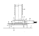
- a circular liquid storage container 61 that opens upward is placed.
- the bottom surface of the container 61 is provided with a pad 6 having a catalyst layer formed on the entire surface with a predetermined thickness by sputtering or the like.
- a pad 6 having a catalyst layer formed on the entire surface with a predetermined thickness by sputtering or the like.
- rubber, urethane, or the like that is resistant to the processing solution is used.
- a transition metal such as Pt can be used as the catalyst.
- the pad 6 may have a diameter slightly larger than the outer diameter of the substrate 7 to be processed.
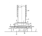
- a main shaft 9 having a circular cross section is suspended above the container 61, and the main shaft 9 is rotatably held by the sleeve 91 in a vertical posture.
- the main shaft 9 is rotated by a drive motor 101 (FIG. 1) as first drive means.
- the sleeve 91 is moved up and down by a drive cylinder 102 as third drive means, and the main shaft 9 is moved back and forth with respect to the pad 6 in response to this.
- FIG. 4 Details of the holder 8 are shown in FIG. In FIG. 4, a disc-like base 82 is mounted on the lower end surface of the main shaft 9 with a ball 81 in the center so that the angle can be changed with respect to the lower end surface.
- a wall-like retainer 83 is vertically suspended.
- a cover body 84 projects outwardly and upwardly from the entire outer periphery of the retainer 83.
- the substrate 7 to be processed is accommodated in a retainer 83, and a diaphragm 85 is located behind the substrate 82 between the substrate 82 and the substrate 82.
- the compressed air is supplied into the diaphragm 85 through the air supply pipe 86, and the substrate 7 is pressed against the surface of the pad 6 by the pressing force of the expanded diaphragm 85 in a state where the main shaft 9 is lowered.
- the diaphragm 85 is formed with a plurality of suction holes, and when the main shaft 9 is raised, the inside of the diaphragm 85 is evacuated and the substrate 7 to be processed is attracted to the suction holes and held in the holder 8. It is like that.
- the container 61 When flat processing of the lower surface (processed surface) of the substrate 7 to be processed is performed with the flat processing apparatus having such a structure, the container 61 is filled with a liquid necessary for a catalytic reaction, such as HF, HCl, pure water, or the like.
- the main shaft 9, that is, the substrate 7 to be processed is rotated, and at the same time, the container 61 on the support substrate 4 is linearly reciprocated along the rail 31 in the horizontal direction. That is, the processing surface of the substrate 7 to be processed and the pad 6 on which the catalyst layer with which the substrate 7 abuts are relatively rotated and reciprocated in a plane intersecting the rotation axis.
- the surface to be processed of the substrate 7 to be processed is flattened with high accuracy of the atomic level by catalyst-assisted chemical processing.
- the relationship between the rotational speed of the relative rotation and the relative reciprocation is that the outer peripheral movement distance of the substrate 7 to be processed is 120% or less (excluding 0%) of the reciprocation movement distance of the relative reciprocation. good.
- the moving range of the reciprocating movement may originally be a small one of several atoms level, but is determined in consideration of mechanical constraints and frequency.
- the surface of the pad 6 is only reciprocally moved. Such a large circumferential force is not applied to the substrate 7 to be processed. Therefore, there is no problem that the substrate to be processed is separated from the holder and is sandwiched between the retainers outside and damaged as in the prior art.
- Example and comparative example based on this embodiment A SiC substrate having an outer diameter of 6 inches was used as the substrate 7 to be processed, and flat processing was performed using ultrapure water as a liquid necessary for the catalytic reaction.
- a Pt film was formed as a catalyst layer on the surface of the pad 6 having a diameter of 160 mm.
- the substrate 7 to be processed was rotated, and the support substrate 4 (that is, the pad 6) was reciprocated.
- FIG. 5 shows another example of the flat processing apparatus.
- FIG. 5 corresponds to FIG. 2 of the first embodiment, and the same reference numerals denote the same parts.
- a piston vibrator 59 is provided on the support substrate 4 in the horizontal direction, and the support substrate 4 is reciprocated along the rails 31 by vibration force (vibration).
- vibration force vibration force
- Example and comparative example based on this embodiment A GaN substrate having an outer diameter of 2 inches was used as the substrate 7 to be processed, and flat processing was performed using ultrapure water as a liquid necessary for the catalytic reaction. A Pt film was formed as a catalyst layer on the surface of the pad 6 having a diameter of 53 mm. In this state, the substrate 7 to be processed was rotated, and the support substrate 4 (that is, the pad 6) was reciprocated. And the state of the to-be-processed surface of the to-be-processed substrate 7 was observed with the non-contact three-dimensional surface shape measuring apparatus (Zygo New View 6300 by the US Zygo company).
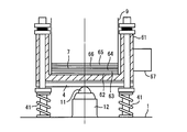
- the support substrate 4 is disposed on the base 1 with the bottom corners supported by the coiled spring material 41, and a container 61 for storing liquid is provided on the support substrate 4.
- a cushion layer 63 and a pad 64 are placed on the cushion layer 63 via an adhesive tape layer 62 from the bottom side, and the substrate 7 to be processed is placed on the upper surface of the pad 64.
- the center of the lower surface of the support substrate 4 is placed on the top of the support member 11 that protrudes upward, and can swing within the three-dimensional space.
- the support member 11 is held by a holding member 12 on the base 1.
- a vibrator 67 is mounted on the side surface of the container 61.
- the main shaft 9 enters the container 61 from above, and a pad 66 is joined to the lower surface of the main shaft 9 via a cushion layer 65.
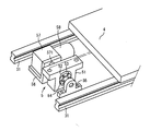
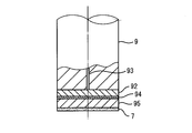
- FIG. 7 shows another example of the holding structure of the substrate 7 to be processed at the lower end of the main shaft 9.
- a header plate 92 is fixed to the lower end of the main shaft 9.
- a plurality of small holes are formed on the lower surface of the header plate 92, and the small holes are formed in the header plate 92.
- a flow path that branches and communicates is formed.
- a flow path 93 is formed in the main shaft 9 and communicates with the flow path in the header plate 92.
- a holding plate 95 made of rubber or the like is provided on the lower surface of the header plate 92 via an adhesive tape layer 94, and a flow path is formed in the holding plate 95 so as to penetrate the small hole. Each flow path opens as a suction hole on the lower surface of the holding plate 95.
- the substrate 7 to be processed when the inside of the flow path 93 is evacuated, the substrate 7 to be processed can be sucked and held on the lower surface of the holding plate 95 with the suction holes as shown in FIG. 7, and this state has been described in the first embodiment. Such flat processing can be performed.
- compressed air or the like is supplied into the flow path 93.
- the substrate to be processed is rotated and the pad is reciprocated linearly.
- the substrate to be processed may be reciprocated linearly and the pad may be rotated.
- the reciprocating drive mechanism is not limited to that of the first embodiment, and a normal crank mechanism that changes the rotational motion of the drive motor to a linear reciprocating motion can be used.
- a ball screw mechanism, a magnetic force repulsion mechanism, a cylinder mechanism, or the like can be used.
- the reciprocation does not necessarily have to be linear.
- an arc may be drawn in a two-dimensional plane such as a circular motion.
- the base may be reciprocated in a direction parallel to the base surface by a ball screw mechanism or the like. In this way, the flattening of the substrate to be processed is made more uniform at the center and the outer periphery.
- the workpiece is not limited to a plate-like object such as a substrate.
- the holder is moved up and down, but a structure in which the support substrate is moved up and down may be used.
- a separate pad is provided in the liquid storage container.
- the pad itself may be formed in a container shape so that the liquid required for the catalytic reaction can be stored. Note that the liquid does not necessarily have to be stored, and may be poured between the substrate to be processed and the pad.
- a drive cylinder is used as the third drive means, but a ball screw mechanism, a robot arm, or the like can be used instead.
Abstract
Description
図1には本発明方法を実施する平坦加工装置の正面図を示し、図2にはその側面図を示す。図1において、基台1上に対称形のL字断面とした架台21,22が左右位置に平行に配設されて、図1の前後方向(図2の左右方向)へ延びており、左右の架台21,22上にはこれらに沿ってそれぞれリニアガイド3を構成するレール31が固定されている。レール31には長手方向の二箇所にこれに沿って摺動移動可能なスライダ32が設けられており、左右前後のスライダ32上に第2保持手段としての四角形の支持基板4が載設されている。これにより、支持基板4はレール31に沿って往復直線移動可能である。
被加工基板7として外径6インチのSiC基板を使用し、触媒反応に必要な液体として超純水を使用して平坦加工を行った。直径160mmのパッド6の表面には触媒層としてPt膜を形成した。この状態で被加工基板7を回転させ、支持基板4(すなわちパッド6)を往復動させた。そして、被加工基板7の被加工面の様子を非接触三次元表面形状測定装置(米国ザイゴ社製Zygo New View 6300)で観察した。それによると、被加工面の全面に亘って、視野0.11mm角においてRa=0.181nm、RMS=0.228nm以内であった。
図5には平坦加工装置の他の例を示す。なお、図5は第1実施形態の図2に対応するもので、同一符号は同一部分を示す。本実施形態では第1実施形態の往復駆動機構5に代えて、支持基板4上にピストンバイブレータ59を水平方向へ設けて、その起振力によって支持基板4をレール31に沿って往復移動(振動)させる。このような構造によっても第1実施形態と同様に、触媒支援型化学加工により被加工基板7の基板面が原子レベル程度の高い精度で平坦加工され、しかも、往復駆動の構造の簡素化が可能になる。
被加工基板7として外径2インチのGaN基板を使用し、触媒反応に必要な液体として超純水を使用して平坦加工を行った。直径53mmのパッド6の表面には触媒層としてPt膜を形成した。この状態で被加工基板7を回転させ、支持基板4(すなわちパッド6)を往復動させた。そして、被加工基板7の被加工面の様子を非接触三次元表面形状測定装置(米国ザイゴ社製Zygo New View 6300)で観察した。それによると、被加工面の全面に亘って、視野0.54mm角においてRa=0.3nm、RMS=0.4nm以内であった。次に走査型プローブ顕微鏡(米国ブルカーAXS社製Dimension Edge)で観察した。それによると、視野2μm角において図8に示すようにGaの1原子層ごとのステップテラス(0.26nm)が確認できた。また、この平坦化加工の間、被加工基板7がホルダ8から引き離されて破損する不具合は生じなかった。
図6において、基台1上にはコイル状ばね材41によって下面四隅を支持されて支持基板4が配設されており、支持基板4上に液貯留用の容器61が設けられている。容器61内には底面側から粘着テープ層62を介してクッション層63とその上にパッド64が載置され、パッド64の上面に被加工基板7が載置されている。支持基板4は下面中央が、上方へ凸状をなす支持部材11の頂部に載置されて三次元空間内で揺動可能となっている。支持部材11は基台1上の保持部材12に保持されている。容器61には側面にバイブレータ67が装着してある。主軸9は上方から容器61内に進入しており、その下面にはクッション層65を介してパッド66が接合されている。
図7には主軸9の下端における被加工基板7の保持構造の他の例を示す。図7において、主軸9の下端にはヘッダ板92が止着されており、ヘッダ板92には下面に複数の小孔(図示略)が形成されるとともにヘッダ板92内には上記小孔に分岐連通する流路が形成されている。主軸9には流路93が形成されてヘッダ板92内の流路に連通している。ヘッダ板92の下面には粘着テープ層94を介してゴム製等の保持板95が設けられており、保持板95内にはこれを貫通して上記小孔に通じる流路が形成されるとともに各流路は保持板95の下面に吸着孔として開口している。
上記第1実施形態では、被加工基板を回転させ、パッドを直線往復動させたが、被加工基板を直線往復動させ、パッドを回転させるようにしても良い。
往復駆動機構は上記第1実施形態のものに限られるものではなく、駆動モータの回転運動を直線往復運動に変える通常のクランク機構が使用できる。さらには、ボールねじ機構、磁力による吸引反発機構やシリンダ機構等を使用することができる。また、往復動は必ずしも直線的である必要は無い。例えば、円運動等の二次元平面内で弧を描くようなものであっても良い。さらには、往復動とする必要は必ずしもなく、一方向での移動としても良い。
上記各実施形態において、基台をさらにボールねじ機構等によって基台面に平行な方向へ往復移動させるようにしても良い。このようにすると、被加工基板の平坦化が中心部と外周部でより均等化される。
被加工物は基板のような板状のものに限定されない。
上記各実施形態ではホルダを昇降移動させるようにしたが、支持基板を昇降移動させる構造としても良い。
上記第1実施形態では液貯留用の容器内に別体のパッドを設けたが、パッド自体を容器状に形成して触媒反応に必要な液体を貯留できるようにしても良い。なお、液は必ずしも貯留する必要は無く、被加工基板とパッドの間にかけ流し状態としても良い。
上記第1実施形態では第3駆動手段として駆動シリンダを使用したが、これに代えてボールねじ機構やロボットアーム等を使用することができる。
Claims (9)
- 被加工物の表面と、少なくとも表面に触媒層を有するパッドの当該表面とを互いに当接ないし近接させ、前記被加工物の表面と前記パッドの表面との間に触媒反応に必要な液体を供給しつつ、前記被加工物ないし前記パッドの一方をその表面内で当該表面に交差する軸回りに回転させるとともに、前記被加工物ないし前記パッドの他方をその表面に平行な方向で少なくとも触媒反応による平坦化が可能な量だけ移動させることを特徴とする平坦加工方法。
- 前記表面に平行な方向での移動は往復動である請求項1に記載の平坦加工方法。
- 回転させられる前記被加工物ないし前記パッドの一方の外周移動距離が、表面に平行な方向で移動させられる前記被加工物ないし前記パッドの他方の移動距離の120%以下(但し0%を除く)になるように設定した請求項1又は2に記載の平坦化加工方法。
- 被加工物の表面と、少なくとも表面に触媒層を有するパッドの当該表面とを互いに当接ないし近接させ、前記被加工物の表面と前記パッドの表面との間に触媒反応に必要な液体を供給しつつ、前記被加工物ないし前記パッドをこれらの表面内で当該表面に交差する軸回りに相対回転させるとともに、前記表面に平行な方向で少なくとも触媒反応による平坦化が可能な量だけ相対移動させることを特徴とする平坦加工方法。
- 被加工物ないし少なくとも表面に触媒層を有するパッドの一方の裏面を保持する第1保持手段と、前記被加工物ないし前記パッドの一方の表面内で当該表面に交差する軸回りに前記被加工物ないし前記パッドの一方を回転させる第1駆動手段と、前記被加工物ないし前記パッドの他方を保持してその表面を、前記被加工物ないし前記パッドの一方の表面に対向位置させる第2保持手段と、前記第2保持手段を前記被加工物ないし前記パッドの他方の表面に平行な方向で少なくとも触媒反応による平坦化が可能な量だけ移動させる第2駆動手段と、前記第1保持手段ないし前記第2保持手段を前記被加工物ないし前記パッドの表面に交差する方向へ前進させて前記被加工物の表面と前記パッドの表面を互いに当接ないし近接させる第3駆動手段とを備える平坦加工装置。
- 前記表面に平行な方向での移動は往復動である請求項5に記載の平坦加工装置。
- 回転させられる前記被加工物ないし前記パッドの一方の外周移動距離が、表面に平行な方向で移動させられる前記被加工物ないし前記パッドの他方の移動距離の120%以下(但し0%を除く)になるように設定されている請求項5又は6に記載の平坦化加工装置。
- 被加工物ないし少なくとも表面に触媒層を有するパッドの一方の裏面を保持する第1保持手段と、前記被加工物ないし前記パッドの他方を保持してその表面を、前記被加工物ないし前記パッドの一方の表面に対向位置させる第2保持手段と、前記第2保持手段を前記被加工物ないし前記パッドの他方の表面に平行な方向で少なくとも触媒反応による平坦化が可能な量だけ移動させるとともに前記被加工物ないし前記パッドの一方の表面内で当該表面に交差する軸回りに回転させる第1駆動手段と、前記第1保持手段ないし前記第2保持手段を前記被加工物ないし前記パッドの表面に交差する方向へ前進させて前記被加工物の表面と前記パッドの表面を互いに当接ないし近接させる第2駆動手段とを備える平坦加工装置。
- 請求項1ないし請求項4のいずれか一つに記載の平坦加工方法に使用するパッド。
Priority Applications (4)
| Application Number | Priority Date | Filing Date | Title |
|---|---|---|---|
| JP2016528258A JP6127235B2 (ja) | 2014-12-31 | 2015-12-28 | 触媒支援型化学加工方法および触媒支援型化学加工装置 |
| US15/315,864 US10199242B2 (en) | 2014-12-31 | 2015-12-28 | Planarizing processing method and planarizing processing device |
| DE112015002319.4T DE112015002319T5 (de) | 2014-12-31 | 2015-12-28 | Planarisierungsbearbeitungsverfahren und Planarisierungsbearbeitungsvorrichtung |
| US16/227,270 US10665480B2 (en) | 2014-12-31 | 2018-12-20 | Planarizing processing method and planarizing processing device |
Applications Claiming Priority (2)
| Application Number | Priority Date | Filing Date | Title |
|---|---|---|---|
| JP2014267111 | 2014-12-31 | ||
| JP2014-267111 | 2014-12-31 |
Related Child Applications (2)
| Application Number | Title | Priority Date | Filing Date |
|---|---|---|---|
| US15/315,864 A-371-Of-International US10199242B2 (en) | 2014-12-31 | 2015-12-28 | Planarizing processing method and planarizing processing device |
| US16/227,270 Division US10665480B2 (en) | 2014-12-31 | 2018-12-20 | Planarizing processing method and planarizing processing device |
Publications (1)
| Publication Number | Publication Date |
|---|---|
| WO2016108284A1 true WO2016108284A1 (ja) | 2016-07-07 |
Family
ID=56284438
Family Applications (1)
| Application Number | Title | Priority Date | Filing Date |
|---|---|---|---|
| PCT/JP2015/086493 WO2016108284A1 (ja) | 2014-12-31 | 2015-12-28 | 平坦加工方法および平坦加工装置 |
Country Status (4)
| Country | Link |
|---|---|
| US (2) | US10199242B2 (ja) |
| JP (2) | JP6127235B2 (ja) |
| DE (1) | DE112015002319T5 (ja) |
| WO (1) | WO2016108284A1 (ja) |
Cited By (1)
| Publication number | Priority date | Publication date | Assignee | Title |
|---|---|---|---|---|
| CN111015504A (zh) * | 2019-12-02 | 2020-04-17 | 深圳市凯合达智能设备有限公司 | 一种具有防护功能的化学机械抛光设备 |
Families Citing this family (4)
| Publication number | Priority date | Publication date | Assignee | Title |
|---|---|---|---|---|
| DE112015002319T5 (de) * | 2014-12-31 | 2017-02-09 | Osaka University | Planarisierungsbearbeitungsverfahren und Planarisierungsbearbeitungsvorrichtung |
| JP6187948B1 (ja) | 2016-03-11 | 2017-08-30 | 東邦エンジニアリング株式会社 | 平坦加工装置、その動作方法および加工物の製造方法 |
| JP7270919B2 (ja) * | 2018-07-20 | 2023-05-11 | 株式会社東邦鋼機製作所 | 加工用ヘッド |
| CN116585976B (zh) * | 2023-05-29 | 2023-12-05 | 湖北嘉裕生物技术有限公司 | 一种造粒抛光一体机 |
Citations (2)
| Publication number | Priority date | Publication date | Assignee | Title |
|---|---|---|---|---|
| JP2009184088A (ja) * | 2008-02-08 | 2009-08-20 | Nikon Corp | 研磨装置 |
| JP2014038981A (ja) * | 2012-08-20 | 2014-02-27 | Toho Engineering Kk | 基板研磨装置 |
Family Cites Families (42)
| Publication number | Priority date | Publication date | Assignee | Title |
|---|---|---|---|---|
| US5245790A (en) * | 1992-02-14 | 1993-09-21 | Lsi Logic Corporation | Ultrasonic energy enhanced chemi-mechanical polishing of silicon wafers |
| ES2109464T3 (es) | 1993-09-06 | 1998-01-16 | Voumard Machines Co Sa | Procedimiento y dispositivo de mecanizado, en particular rectificadora con movimiento oscilante equilibrado. |
| US5938504A (en) * | 1993-11-16 | 1999-08-17 | Applied Materials, Inc. | Substrate polishing apparatus |
| TW375550B (en) | 1997-06-19 | 1999-12-01 | Komatsu Denshi Kinzoku Kk | Polishing apparatus for semiconductor wafer |
| JP2000158331A (ja) | 1997-12-10 | 2000-06-13 | Canon Inc | 基板の精密研磨方法および装置 |
| JP2000033555A (ja) * | 1998-07-17 | 2000-02-02 | Sony Corp | 研磨装置 |
| US7516536B2 (en) | 1999-07-08 | 2009-04-14 | Toho Engineering Kabushiki Kaisha | Method of producing polishing pad |
| US6869343B2 (en) | 2001-12-19 | 2005-03-22 | Toho Engineering Kabushiki Kaisha | Turning tool for grooving polishing pad, apparatus and method of producing polishing pad using the tool, and polishing pad produced by using the tool |
| US6722963B1 (en) | 1999-08-03 | 2004-04-20 | Micron Technology, Inc. | Apparatus for chemical-mechanical planarization of microelectronic substrates with a carrier and membrane |
| JP2001345297A (ja) | 2000-05-30 | 2001-12-14 | Hitachi Ltd | 半導体集積回路装置の製造方法及び研磨装置 |
| US6527625B1 (en) | 2000-08-31 | 2003-03-04 | Multi-Planar Technologies, Inc. | Chemical mechanical polishing apparatus and method having a soft backed polishing head |
| US6540590B1 (en) | 2000-08-31 | 2003-04-01 | Multi-Planar Technologies, Inc. | Chemical mechanical polishing apparatus and method having a rotating retaining ring |
| JP4060043B2 (ja) | 2001-03-28 | 2008-03-12 | 株式会社Sumco | 研磨装置 |
| US6585562B2 (en) * | 2001-05-17 | 2003-07-01 | Nevmet Corporation | Method and apparatus for polishing control with signal peak analysis |
| WO2003083918A1 (fr) | 2002-04-03 | 2003-10-09 | Toho Engineering Kabushiki Kaisha | Tampon a polir et procede de fabrication de substrat a semi-conducteurs utilisant ce tampon a polir |
| JP2004017229A (ja) | 2002-06-18 | 2004-01-22 | Shimadzu Corp | 基板研磨装置 |
| JP2004223636A (ja) | 2003-01-21 | 2004-08-12 | Nikon Corp | 研磨方法、研磨装置、研磨シミュレーション方法、半導体デバイス、及び半導体デバイスの製造方法 |
| US20050247673A1 (en) | 2004-05-07 | 2005-11-10 | International Business Machines Corporation | Confinement of fluids on surfaces |
| JP4506399B2 (ja) * | 2004-10-13 | 2010-07-21 | 株式会社荏原製作所 | 触媒支援型化学加工方法 |
| JP3872081B2 (ja) | 2004-12-29 | 2007-01-24 | 東邦エンジニアリング株式会社 | 研磨用パッド |
| JP4873694B2 (ja) | 2006-04-12 | 2012-02-08 | 国立大学法人 熊本大学 | 触媒支援型化学加工方法 |
| JP5007791B2 (ja) | 2006-08-24 | 2012-08-22 | 住友金属鉱山株式会社 | ウエハーの研磨方法 |
| JP2008081389A (ja) | 2006-08-28 | 2008-04-10 | Osaka Univ | 触媒支援型化学加工方法及び装置 |
| JP2008136983A (ja) | 2006-12-05 | 2008-06-19 | Osaka Univ | 触媒支援型化学加工方法及び加工装置 |
| JP5007384B2 (ja) | 2006-10-18 | 2012-08-22 | 株式会社荏原製作所 | 触媒支援型化学加工方法及び装置 |
| EP2381008A2 (en) | 2006-08-28 | 2011-10-26 | Osaka University | Catalyst-aided chemical processing method and apparatus |
| JP4982742B2 (ja) * | 2006-09-13 | 2012-07-25 | 国立大学法人 熊本大学 | 磁性微粒子を用いた触媒化学加工方法及び装置 |
| JP4887266B2 (ja) | 2007-10-15 | 2012-02-29 | 株式会社荏原製作所 | 平坦化方法 |
| JP5632132B2 (ja) | 2009-02-27 | 2014-11-26 | 株式会社荏原製作所 | 基板処理方法 |
| KR101754550B1 (ko) | 2009-12-15 | 2017-07-05 | 고꾸리쯔 다이가꾸 호우징 오사까 다이가꾸 | 연마 공구 및 연마 장치 |
| JP4680314B1 (ja) | 2010-02-04 | 2011-05-11 | 東邦エンジニアリング株式会社 | 研磨パッド用補助板およびそれを用いた研磨パッドの再生方法 |
| DE102010032335A1 (de) | 2010-07-20 | 2012-01-26 | C. & E. Fein Gmbh | Handwerkzeug |
| US9291056B2 (en) | 2010-08-30 | 2016-03-22 | Lawrence Livermore National Security, Llc | Harmonic uniflow engine |
| JP2012235072A (ja) | 2011-05-09 | 2012-11-29 | Sumco Corp | ウェーハ表面処理方法 |
| JP5789869B2 (ja) | 2011-07-28 | 2015-10-07 | 東邦エンジニアリング株式会社 | 研磨パッド用補助板および研磨パッド用補助板を備えた研磨装置 |
| US20130288577A1 (en) | 2012-04-27 | 2013-10-31 | Applied Materials, Inc. | Methods and apparatus for active substrate precession during chemical mechanical polishing |
| JP2013255961A (ja) | 2012-06-12 | 2013-12-26 | Takatori Corp | 基板の研磨装置 |
| JP6282437B2 (ja) | 2012-10-18 | 2018-02-21 | アプライド マテリアルズ インコーポレイテッドApplied Materials,Incorporated | 研磨パッドコンディショナ用ダンパ |
| JP6225991B2 (ja) * | 2013-07-19 | 2017-11-15 | 国立大学法人 名古屋工業大学 | 金属製研磨パッドおよびその製造方法 |
| JP6206847B2 (ja) * | 2014-03-12 | 2017-10-04 | 国立大学法人大阪大学 | ワイドバンドギャップ半導体基板の加工方法及びその装置 |
| KR102120687B1 (ko) | 2014-04-18 | 2020-06-09 | 가부시키가이샤 에바라 세이사꾸쇼 | 기판 처리 장치, 기판 처리 시스템 및 기판 처리 방법 |
| DE112015002319T5 (de) * | 2014-12-31 | 2017-02-09 | Osaka University | Planarisierungsbearbeitungsverfahren und Planarisierungsbearbeitungsvorrichtung |
-
2015
- 2015-12-28 DE DE112015002319.4T patent/DE112015002319T5/de active Pending
- 2015-12-28 US US15/315,864 patent/US10199242B2/en active Active
- 2015-12-28 WO PCT/JP2015/086493 patent/WO2016108284A1/ja active Application Filing
- 2015-12-28 JP JP2016528258A patent/JP6127235B2/ja active Active
-
2017
- 2017-02-28 JP JP2017035605A patent/JP2017100280A/ja active Pending
-
2018
- 2018-12-20 US US16/227,270 patent/US10665480B2/en active Active
Patent Citations (2)
| Publication number | Priority date | Publication date | Assignee | Title |
|---|---|---|---|---|
| JP2009184088A (ja) * | 2008-02-08 | 2009-08-20 | Nikon Corp | 研磨装置 |
| JP2014038981A (ja) * | 2012-08-20 | 2014-02-27 | Toho Engineering Kk | 基板研磨装置 |
Cited By (1)
| Publication number | Priority date | Publication date | Assignee | Title |
|---|---|---|---|---|
| CN111015504A (zh) * | 2019-12-02 | 2020-04-17 | 深圳市凯合达智能设备有限公司 | 一种具有防护功能的化学机械抛光设备 |
Also Published As
| Publication number | Publication date |
|---|---|
| US10199242B2 (en) | 2019-02-05 |
| DE112015002319T5 (de) | 2017-02-09 |
| US10665480B2 (en) | 2020-05-26 |
| US20190122904A1 (en) | 2019-04-25 |
| US20170098559A1 (en) | 2017-04-06 |
| JPWO2016108284A1 (ja) | 2017-04-27 |
| JP2017100280A (ja) | 2017-06-08 |
| JP6127235B2 (ja) | 2017-05-17 |
Similar Documents
| Publication | Publication Date | Title |
|---|---|---|
| JP6127235B2 (ja) | 触媒支援型化学加工方法および触媒支援型化学加工装置 | |
| JP6187948B1 (ja) | 平坦加工装置、その動作方法および加工物の製造方法 | |
| EP1738870A1 (en) | Polisher | |
| JP6018656B2 (ja) | 研磨装置および研磨方法 | |
| TW201522186A (zh) | 晶圓處理系統及處理晶圓之方法 | |
| CN107248500B (zh) | 一种取晶、固晶装置及其采用它的固晶机 | |
| JP2012183637A (ja) | 基板を処理する方法及び装置 | |
| JP2018001406A (ja) | 研磨装置及び研磨方法 | |
| KR101324886B1 (ko) | 초음파를 이용하는 유리연마장치 | |
| TWM441208U (en) | Processing device for plate | |
| JP2017163144A (ja) | 平坦加工装置 | |
| JP2016013601A (ja) | 研磨装置 | |
| JP5433968B2 (ja) | 保持装置、研磨装置および保持方法 | |
| JP6044955B2 (ja) | ウェーハ研磨ヘッドおよびウェーハ研磨装置 | |
| JP6072591B2 (ja) | 加工装置 | |
| CN215656627U (zh) | 晶圆清洗机 | |
| JP2017087305A (ja) | 円板状ワークの研磨加工方法及び研磨加工装置 | |
| JP2010000553A (ja) | 蛇腹機構および加工装置 | |
| JP6573168B2 (ja) | 板ガラスの製造方法及び製造装置 | |
| JP6573381B2 (ja) | 研磨装置 |
Legal Events
| Date | Code | Title | Description |
|---|---|---|---|
| ENP | Entry into the national phase |
Ref document number: 2016528258 Country of ref document: JP Kind code of ref document: A |
|
| 121 | Ep: the epo has been informed by wipo that ep was designated in this application |
Ref document number: 15875410 Country of ref document: EP Kind code of ref document: A1 |
|
| WWE | Wipo information: entry into national phase |
Ref document number: 15315864 Country of ref document: US |
|
| WWE | Wipo information: entry into national phase |
Ref document number: 112015002319 Country of ref document: DE |
|
| 122 | Ep: pct application non-entry in european phase |
Ref document number: 15875410 Country of ref document: EP Kind code of ref document: A1 |