US10665480B2 - Planarizing processing method and planarizing processing device - Google Patents
Planarizing processing method and planarizing processing device Download PDFInfo
- Publication number
- US10665480B2 US10665480B2 US16/227,270 US201816227270A US10665480B2 US 10665480 B2 US10665480 B2 US 10665480B2 US 201816227270 A US201816227270 A US 201816227270A US 10665480 B2 US10665480 B2 US 10665480B2
- Authority
- US
- United States
- Prior art keywords
- workpiece
- pad
- processing method
- planarization processing
- reciprocating motion
- Prior art date
- Legal status (The legal status is an assumption and is not a legal conclusion. Google has not performed a legal analysis and makes no representation as to the accuracy of the status listed.)
- Active, expires
Links
- 238000012545 processing Methods 0.000 title claims description 41
- 238000003672 processing method Methods 0.000 title claims description 26
- 239000003054 catalyst Substances 0.000 claims abstract description 18
- 238000006555 catalytic reaction Methods 0.000 claims abstract description 14
- 239000007788 liquid Substances 0.000 claims abstract description 12
- JMASRVWKEDWRBT-UHFFFAOYSA-N Gallium nitride Chemical compound [Ga]#N JMASRVWKEDWRBT-UHFFFAOYSA-N 0.000 claims description 3
- 150000003623 transition metal compounds Chemical class 0.000 claims 3
- 238000000034 method Methods 0.000 abstract description 12
- 239000000758 substrate Substances 0.000 description 52
- 230000007246 mechanism Effects 0.000 description 14
- 238000012993 chemical processing Methods 0.000 description 6
- 230000000694 effects Effects 0.000 description 3
- 230000008569 process Effects 0.000 description 3
- 229910052723 transition metal Inorganic materials 0.000 description 3
- 150000003624 transition metals Chemical class 0.000 description 3
- 239000002390 adhesive tape Substances 0.000 description 2
- 239000003638 chemical reducing agent Substances 0.000 description 2
- 230000000052 comparative effect Effects 0.000 description 2
- 150000001875 compounds Chemical class 0.000 description 2
- 230000004044 response Effects 0.000 description 2
- 239000000523 sample Substances 0.000 description 2
- 229910021642 ultra pure water Inorganic materials 0.000 description 2
- 239000012498 ultrapure water Substances 0.000 description 2
- 238000012935 Averaging Methods 0.000 description 1
- JOYRKODLDBILNP-UHFFFAOYSA-N Ethyl urethane Chemical compound CCOC(N)=O JOYRKODLDBILNP-UHFFFAOYSA-N 0.000 description 1
- 239000006061 abrasive grain Substances 0.000 description 1
- 238000013459 approach Methods 0.000 description 1
- 238000006243 chemical reaction Methods 0.000 description 1
- 230000003247 decreasing effect Effects 0.000 description 1
- 238000013461 design Methods 0.000 description 1
- 238000005530 etching Methods 0.000 description 1
- 239000000463 material Substances 0.000 description 1
- 230000002093 peripheral effect Effects 0.000 description 1
- 238000000926 separation method Methods 0.000 description 1
- 238000004544 sputter deposition Methods 0.000 description 1
- 230000003746 surface roughness Effects 0.000 description 1
- XLYOFNOQVPJJNP-UHFFFAOYSA-N water Substances O XLYOFNOQVPJJNP-UHFFFAOYSA-N 0.000 description 1
Images


Classifications
-
- H—ELECTRICITY
- H01—ELECTRIC ELEMENTS
- H01L—SEMICONDUCTOR DEVICES NOT COVERED BY CLASS H10
- H01L21/00—Processes or apparatus adapted for the manufacture or treatment of semiconductor or solid state devices or of parts thereof
- H01L21/67—Apparatus specially adapted for handling semiconductor or electric solid state devices during manufacture or treatment thereof; Apparatus specially adapted for handling wafers during manufacture or treatment of semiconductor or electric solid state devices or components ; Apparatus not specifically provided for elsewhere
- H01L21/67005—Apparatus not specifically provided for elsewhere
- H01L21/67011—Apparatus for manufacture or treatment
- H01L21/67017—Apparatus for fluid treatment
- H01L21/67063—Apparatus for fluid treatment for etching
- H01L21/67075—Apparatus for fluid treatment for etching for wet etching
-
- B—PERFORMING OPERATIONS; TRANSPORTING
- B01—PHYSICAL OR CHEMICAL PROCESSES OR APPARATUS IN GENERAL
- B01J—CHEMICAL OR PHYSICAL PROCESSES, e.g. CATALYSIS OR COLLOID CHEMISTRY; THEIR RELEVANT APPARATUS
- B01J23/00—Catalysts comprising metals or metal oxides or hydroxides, not provided for in group B01J21/00
- B01J23/38—Catalysts comprising metals or metal oxides or hydroxides, not provided for in group B01J21/00 of noble metals
- B01J23/40—Catalysts comprising metals or metal oxides or hydroxides, not provided for in group B01J21/00 of noble metals of the platinum group metals
- B01J23/42—Platinum
-
- B—PERFORMING OPERATIONS; TRANSPORTING
- B01—PHYSICAL OR CHEMICAL PROCESSES OR APPARATUS IN GENERAL
- B01J—CHEMICAL OR PHYSICAL PROCESSES, e.g. CATALYSIS OR COLLOID CHEMISTRY; THEIR RELEVANT APPARATUS
- B01J35/00—Catalysts, in general, characterised by their form or physical properties
-
- B—PERFORMING OPERATIONS; TRANSPORTING
- B01—PHYSICAL OR CHEMICAL PROCESSES OR APPARATUS IN GENERAL
- B01J—CHEMICAL OR PHYSICAL PROCESSES, e.g. CATALYSIS OR COLLOID CHEMISTRY; THEIR RELEVANT APPARATUS
- B01J35/00—Catalysts, in general, characterised by their form or physical properties
- B01J35/02—Solids
-
- B01J35/30—
-
- H—ELECTRICITY
- H01—ELECTRIC ELEMENTS
- H01L—SEMICONDUCTOR DEVICES NOT COVERED BY CLASS H10
- H01L21/00—Processes or apparatus adapted for the manufacture or treatment of semiconductor or solid state devices or of parts thereof
- H01L21/02—Manufacture or treatment of semiconductor devices or of parts thereof
- H01L21/02002—Preparing wafers
- H01L21/02005—Preparing bulk and homogeneous wafers
- H01L21/02008—Multistep processes
- H01L21/0201—Specific process step
- H01L21/02019—Chemical etching
-
- H—ELECTRICITY
- H01—ELECTRIC ELEMENTS
- H01L—SEMICONDUCTOR DEVICES NOT COVERED BY CLASS H10
- H01L21/00—Processes or apparatus adapted for the manufacture or treatment of semiconductor or solid state devices or of parts thereof
- H01L21/02—Manufacture or treatment of semiconductor devices or of parts thereof
- H01L21/02002—Preparing wafers
- H01L21/02005—Preparing bulk and homogeneous wafers
- H01L21/02008—Multistep processes
- H01L21/0201—Specific process step
- H01L21/02024—Mirror polishing
-
- H—ELECTRICITY
- H01—ELECTRIC ELEMENTS
- H01L—SEMICONDUCTOR DEVICES NOT COVERED BY CLASS H10
- H01L21/00—Processes or apparatus adapted for the manufacture or treatment of semiconductor or solid state devices or of parts thereof
- H01L21/02—Manufacture or treatment of semiconductor devices or of parts thereof
- H01L21/04—Manufacture or treatment of semiconductor devices or of parts thereof the devices having at least one potential-jump barrier or surface barrier, e.g. PN junction, depletion layer or carrier concentration layer
- H01L21/18—Manufacture or treatment of semiconductor devices or of parts thereof the devices having at least one potential-jump barrier or surface barrier, e.g. PN junction, depletion layer or carrier concentration layer the devices having semiconductor bodies comprising elements of Group IV of the Periodic System or AIIIBV compounds with or without impurities, e.g. doping materials
- H01L21/30—Treatment of semiconductor bodies using processes or apparatus not provided for in groups H01L21/20 - H01L21/26
- H01L21/302—Treatment of semiconductor bodies using processes or apparatus not provided for in groups H01L21/20 - H01L21/26 to change their surface-physical characteristics or shape, e.g. etching, polishing, cutting
- H01L21/306—Chemical or electrical treatment, e.g. electrolytic etching
- H01L21/30604—Chemical etching
- H01L21/30612—Etching of AIIIBV compounds
-
- H—ELECTRICITY
- H01—ELECTRIC ELEMENTS
- H01L—SEMICONDUCTOR DEVICES NOT COVERED BY CLASS H10
- H01L29/00—Semiconductor devices adapted for rectifying, amplifying, oscillating or switching, or capacitors or resistors with at least one potential-jump barrier or surface barrier, e.g. PN junction depletion layer or carrier concentration layer; Details of semiconductor bodies or of electrodes thereof ; Multistep manufacturing processes therefor
- H01L29/02—Semiconductor bodies ; Multistep manufacturing processes therefor
- H01L29/12—Semiconductor bodies ; Multistep manufacturing processes therefor characterised by the materials of which they are formed
- H01L29/16—Semiconductor bodies ; Multistep manufacturing processes therefor characterised by the materials of which they are formed including, apart from doping materials or other impurities, only elements of Group IV of the Periodic System
- H01L29/1608—Silicon carbide
-
- H—ELECTRICITY
- H01—ELECTRIC ELEMENTS
- H01L—SEMICONDUCTOR DEVICES NOT COVERED BY CLASS H10
- H01L29/00—Semiconductor devices adapted for rectifying, amplifying, oscillating or switching, or capacitors or resistors with at least one potential-jump barrier or surface barrier, e.g. PN junction depletion layer or carrier concentration layer; Details of semiconductor bodies or of electrodes thereof ; Multistep manufacturing processes therefor
- H01L29/02—Semiconductor bodies ; Multistep manufacturing processes therefor
- H01L29/12—Semiconductor bodies ; Multistep manufacturing processes therefor characterised by the materials of which they are formed
- H01L29/20—Semiconductor bodies ; Multistep manufacturing processes therefor characterised by the materials of which they are formed including, apart from doping materials or other impurities, only AIIIBV compounds
- H01L29/2003—Nitride compounds
Definitions
- the present invention relates to a planarization processing method and to a planarization processing device, and particularly to a method and a device that can be suitably employed in planarization processing using a catalyst-aided chemical processing method.
- Catalyst-aided chemical processing methods include using a catalyst composed of a transition metal that is disposed on a processing base surface, placing a workpiece in a solution that does not contain abrasive grains, etc., bringing the processing base surface into contact with or proximal to the processed surface of the workpiece, causing the processing base surface and the processed surface to move relative to each other, producing compounds in a chemical reaction between active species generated from the solution and surface atoms of the workpiece, and removing the compounds to process (etch) the workpiece; it is thereby possible to planarize (reduce the surface roughness of) a surface of difficult-to-process substrates made, for example, of SiC and GaN with high precision approximately at an atomic level.
- Patent Literature 1 Japanese Laid-Open Patent Publication No. 2006-114632
- Patent Literature 2 Japanese Laid-Open Patent Publication No. 2007-283410
- the apparatus is large because the diameter of the pad is at least twice the diameter of the workpiece, and an economical processing is not achieved because it takes a long period of time to process SiC and GaN substrates.
- the processed substrate is rotated while being pressed against the pad surface by the back pressure of an airbag provided in the holder, the processed substrate is pulled towards the pad surface by the so-called water-adhesion effect resulting from the solution that is supplied between the processed substrate and the pad having the catalyst layer of Pt or the like formed on the surface and that is a smooth flat surface; therefore, a large circumferential rotary force of the pad acts on the processed substrate, pulls the processed substrate away from the holder, and hurls it toward the outer circumference of the pad, resulting in a risk of damage by it being caught, etc., on an outwardly-located retainer.
- an object of the present invention is to provide a planarization processing method and a planarization processing device capable of making the device more compact, reducing the risk of workpiece damage during processing and suppressing an increase in processing costs while achieving precise planarization processing.
- a planarization processing method is characterized by comprising: bringing a surface of a workpiece and a surface of a pad having a catalyst layer at least on the surface thereof into contact with or proximal to each other; rotating one of the workpiece and the pad in a plane of the surface thereof and around an axis that intersects the surface; simultaneously moving the other of the workpiece and the pad in a direction parallel to the surface thereof by at least an amount that makes possible planarization based on a catalytic reaction, and supplying a liquid necessary for the catalytic reaction between the surface of the workpiece and the surface of the pad that are in contact with or in proximity to each other.
- the movement in the direction parallel to the surface may be movement that excludes rotation around the above-mentioned axis.
- the movement in the direction parallel to the surface can be a reciprocating movement.
- the travel distance of an outer circumference of the one of the workpiece and the pad, which is rotated may be set so as to be 120% or less (excluding 0%) of the travel distance of the other of the workpiece and the pad, which moves in the direction parallel to the surface. It is noted that, instead of rotating one of the workpiece and the pad and moving the other in the direction parallel to the surface, one of the workpiece and the pad may be kept stationary and the other may be rotated and moved in the direction parallel to the surface.
- planarization processing method when planarization processing is performed using a catalyst-aided chemical processing method, one of the workpiece and the pad is rotated relative to the other and the other is moved relative to the one by at least an amount that makes possible planarization based on a catalytic reaction with the intention of averaging of the etching, whereby precise planarization processing is achieved.
- a travel distance at the atomic-level suffices to make possible the processing. Therefore, it is not necessary to use a large-diameter pad, unlike in the related art; thus, because it is possible to set the outer diameter of the pad to be approximately equal to the outer diameter of the workpiece, the device can be miniaturized.
- a planarization processing device includes first holding means ( 4 ; 8 ) that holds a rear surface of one of a workpiece ( 7 ) and a pad ( 6 ) having a catalyst layer at least on a surface thereof; first drive means ( 101 ) that rotates one of the workpiece ( 7 ) and the pad ( 6 ) in a plane of the surface of the one of the workpiece ( 7 ) and the pad ( 6 ) and around an axis that intersects the surface; second holding means ( 4 ; 8 ) that holds the other of the workpiece ( 7 ) and the pad ( 6 ) and causes the surface thereof to face the surface of the one of the workpiece ( 7 ) and the pad ( 6 ); second drive means ( 5 , 51 - 55 , 58 ; 59 ) that moves the second holding means ( 4 ; 8 ) in a direction parallel to the surface of the other of the workpiece ( 7 ) and the pad ( 6 ) by at least an amount that makes possible planarization
- the movement in the direction parallel to the surface can be a reciprocating movement.
- the travel distance of the outer circumference of the one of the workpiece and the pad, which is rotated may be set to be 120% or less (excluding 0%) of the travel distance of the other of the workpiece and the pad, which moves in the direction parallel to the surface.
- one of the workpiece and the pad may be kept stationary and the other may be rotated and moved in the direction parallel to the surface. Since the planarization processing device according to the present invention can carry out the planarization processing method according to the present invention, the same advantageous effects described above are provided.
- the device while achieving precise planarization processing, the device can be miniaturized, the risk of damage of the workpiece during processing is lessened, and an increase in processing costs can be suppressed.
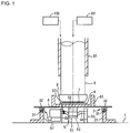
- FIG. 1 is a main portion, partial cross-sectional front view of a planarization processing device in a first embodiment of the present invention.
- FIG. 2 is main portion, partial cross-sectional side view of the planarization processing device.
- FIG. 3 is a perspective view of a reciprocating drive mechanism.
- FIG. 4 is a schematic cross-sectional view of a holder.
- FIG. 5 is a main portion, partial cross-sectional side view of a planarization processing device in a second embodiment of the present invention.
- FIG. 6 is a main portion partial cross-sectional front view of a planarization processing device in a third embodiment of the present invention.
- FIG. 7 is a cutaway enlarged cross-sectional view of a processed substrate holding part of a planarization processing device in a fourth embodiment of the present invention.
- FIG. 8 is a scanning probe microscope photograph of a processed surface of a processed substrate.
- FIG. 1 is a partial cross-sectional front view of a planarization processing device that carries out a method according to the prevent invention
- FIG. 2 is a side view of the planarization processing device.
- stands 21 and 22 which have symmetric letter-L-shaped cross sections, are disposed in parallel to each other on the right and left sides on a base 1 and extend in the forward/rearward direction in FIG. 1 (rightward/leftward direction in FIG. 2 ); rails 31 , which form linear guides 3 , are fixed onto the right and left stands 21 , 22 so as to extend therealong.
- Each of the rails 31 is provided with sliders 32 , which are slidable along the rail 31 , at two locations in the longitudinal direction thereof; a rectangular support plate 4 serving as a second holding means is placed on the right-left, front-rear sliders 32 .
- the support plate 4 is therefore linearly reciprocally movable along the rails 31 .
- a cam block 51 which constitutes a reciprocating drive mechanism 5 that extends downward and will be described below, is fixed to a central portion of the lower surface of the support plate 4 .
- the cam block 51 is a thick protruding body extending in parallel to the rails 31 , as shown in FIG. 3 ; a cam opening 52 , which is elongated in the upward/downward direction, is formed in a longitudinally central portion of the cam block 51 in such a way that the cam opening 52 passes through the cam block 51 in the horizontal direction.
- a cam body 53 which has a circular shape with a diameter approximately equal to the minor diameter of the opening 52 , is provided in the cam opening 52 so as to be movable along the cam opening 52 in the upward/downward direction.
- a crankshaft 54 is provided so as to pass through the above-described cam body 53 in the horizontal direction; the crankshaft 54 passes through the center of the cam body 53 in such a way that the crankshaft 54 can rotate relative to the cam body 53 .
- a central portion of the crankshaft 54 is eccentric from the line that connects the right and left opposite ends of the crankshaft 54 , one end of the crankshaft 54 being rotatably supported by a bearing member 55 , which is provided so as to stand on the base 1 ; the other end of the crankshaft 54 is coupled to an output shaft 571 of a speed reducer 57 , which is fixed, in a horizontal attitude, to an upright wall of a letter-L-shaped support plate 56 .
- a drive motor 58 ( FIG. 3 ) is attached to the speed reducer 57 .
- the cam body 53 which the central portion of the crankshaft 54 passes, undergoes rotating movement in a vertical plane while moving upward and downward in the cam opening 52 .
- the cam block 51 and the support plate 4 which is integral therewith, are caused to undergo linear reciprocating movement in the direction along the rails 31 .
- the reciprocating drive mechanism 5 which produces the linear reciprocating motion described above, is an example of a second drive means.
- a circular container 61 which stores liquid and opens upward, is provided so as to be placed on a central portion of the upper surface of the support plate 4 .
- a pad 6 which has a catalyst layer with a predetermined thickness formed by a sputtering process or the like on the entire surface thereof, is provided on the bottom surface of the container 61 . Rubber or urethane or the like, which is resistant to the processing solution, is used as the material of the pad 6 .
- a transition metal, such as Pt, can be used as the catalyst.
- the diameter of the pad 6 may be set so as to be slightly greater than the outer diameter of a processed substrate 7 .
- a spindle 9 which has a circular cross-sectional shape, is provided above the container 61 so as to be vertically oriented and is held by a sleeve 91 so as to be rotatable with a vertical attitude.
- the spindle 9 is rotated by a drive motor 101 ( FIG. 1 ) serving as a first drive means.
- the sleeve 91 is lifted and lowered by a drive cylinder 102 serving as a third drive means, and the spindle 9 is caused to move frontward and rearward relative to the pad 6 or to approach and move away from the pad 6 in response to the motion of the sleeve 91 .
- a holder 8 serving as a first holding means is provided at the lower end of the spindle 9 and holds the processed substrate 7 .
- the holder 8 is a known holder and will be described below in detail.
- FIG. 4 shows the holder 8 in detail.
- a base body 82 having a circular plate-shape is attached to the lower end surface of the spindle 9 via a ball 81 , which is located at the center of the base body 82 and is interposed between the base body 82 and the lower end surface in such a way that the angle of the base body 82 is changeable with respect to the lower end surface;
- a wall-shaped retainer 83 is provided so as to be vertically oriented and extend along the entire outer circumferential edge of the lower surface of the base body 82 .
- a cover body 84 is provided so as to protrude outward and upward and extend along the entire outer circumference of the retainer 83 .
- the processed substrate 7 is accommodated in the retainer 83 ; a diaphragm 85 is located behind the processed substrate 7 and between the processed substrate 7 and the base body 82 .
- Compressed air is supplied into the diaphragm 85 through an air supply tube 86 so that, when the spindle 9 has been lowered, the processed substrate 7 is pressed against the surface of the pad 6 by a pressing force produced by the inflated diaphragm 85 .
- a plurality of suction holes is formed in the diaphragm 85 ; when the spindle 9 is lifted, the interior of the diaphragm 85 is evacuated, the processed substrate 7 is suctioned towards the suction holes and it is held in the holder 8 .
- a liquid necessary for the catalytic reaction such as HF, HCL, pure water or the like
- the spindle 9 i.e. the processed substrate 7
- the container 61 on the support plate 4 is caused to undergo a linear reciprocating motion in the horizontal direction along the rails 31 . That is, the processed surface of the processed substrate 7 and the pad 6 , which has the contacting catalyst layer formed thereon, are caused to rotate relative to each other and are simultaneously caused to undergo a relative reciprocating motion in a plane that intersects the axis of the rotation.
- the processed surface of the processed substrate 7 thus undergoes planarization processing in accordance with catalyst-aided chemical processing with high precision approximately at an atomic level.
- the relationship between the number of revolutions of the relative rotation and the relative reciprocating motion is preferably set so that the travel distance of the outer circumference of the processed substrate 7 is 120% or less (excluding 0%) of the reciprocating travel distance of the relative reciprocating motion.
- the range of movement of the reciprocating movement may intrinsically be within a minute range at the level of several atoms, it is determined based upon mechanical constraints and vibration frequency.
- An SiC substrate having an outer diameter of 6 inches was used as the processed substrate 7 , and ultrapure water was used as the liquid necessary for the catalytic reaction to perform the planarization processing.
- a Pt film serving as the catalyst layer was formed on the surface of a pad 6 having a diameter of 160 mm.
- the processed substrate 7 was rotated, and the support plate 4 (that is, the pad 6 ) was caused to undergo reciprocating motion.
- the processed surface of the processed substrate 7 after the processing was observed with a noncontact three-dimensional surface profiler (Zygo NewView 6300 manufactured by ZYGO CORPORATION, USA).
- Ra was 0.181 nm or smaller
- RMS was 0.228 nm or smaller, over the entire processed surface and in a field of view of 0.11 mm square.
- FIG. 5 shows another example of a planarization processing device.
- FIG. 5 corresponds to FIG. 2 of the first embodiment, and the same reference symbols represent the same parts.
- a piston vibrator 59 is provided on the support plate 4 in the horizontal direction, and vibratory forces produced by the piston vibrator 59 cause the support plate 4 to undergo reciprocating movement (vibration) along the rails 31 .
- the substrate surface of the processed substrate 7 undergoes planarization processing in accordance with catalyst-aided chemical processing with high precision approximately at an atomic level similar to the first embodiment; moreover, it is possible to simplify the reciprocating drive structure.
- a GaN substrate having an outer diameter of 2 inches was used as the processed substrate 7 , and ultrapure water was used as the liquid necessary for the catalytic reaction to perform the planarization processing.
- a Pt film serving as the catalyst layer was formed on the surface of a pad 6 having a diameter of 53 mm.
- the processed substrate 7 was rotated, and the support plate 4 (that is, the pad 6 ) was caused to undergo reciprocating motion.
- the processed surface of the processed substrate 7 after the processing was observed with the noncontact three-dimensional surface profiler (Zygo NewView 6300 manufactured by ZYGO CORPORATION, USA).
- Ra was 0.3 nm or smaller, and RMS was 0.4 nm or smaller, over the entire processed surface and in a field of view of 0.54 mm square.
- the processed surface was then observed with a scanning probe microscope (Dimension Edge manufactured by BRUKER AXS CORPORATION, USA).
- step terraces (0.26 nm) for each Ga single atom layer in a field of view of 2 ⁇ m square, as shown in FIG. 8 , could be confirmed. Further, during the planarization processing, the problem of separation of the processed substrate 7 from the holder 8 followed by damage of the processed substrate 7 did not occur.
- the support plate 4 is disposed above the base 1 with the four corners of the lower surface of the support plate 4 supported by coil springs 41 , and the liquid storing container 61 is provided on the support plate 4 .
- a cushion layer 63 having a pad 64 thereon is placed in the container 61 on the bottom side via an adhesive tape layer 62 , and the processed substrate 7 is placed on the upper surface of the pad 64 .
- the center of the lower surface of the support plate 4 is placed on the vertex of a support member 11 , which has an upwardly convex shape, so that the support plate 4 is shakeable in the three-dimensional space.
- the support member 11 is held on the base 1 by a holding member 12 .
- a vibrator 67 is attached to the side surface of the container 61 .
- the spindle 9 enters the container 61 from above, and a pad 66 is bonded to the lower surface of the spindle 9 via a cushion layer 65 .
- the spindle 9 is lowered so that the pads 64 and 66 sandwich the upper and lower surfaces of the processed substrate 7 .
- the rotary force of the spindle 9 and a shaking motion which includes a horizontal reciprocating movement (vibration) produced by the vibrator 67 , are transmitted to the processed substrate 7 and to the upper and lower pads 64 , 66 , which sandwich the processed substrate 7 ; thus, either of the upper and lower surfaces of the processed substrate 7 can be planarized with the same precision and uniformity, etc. as in each of the embodiments described above.
- FIG. 7 shows another example of a structure for holding the processed substrate 7 at the lower end of the spindle 9 .
- a header plate 92 is fixed to the lower end of the spindle 9 , a plurality of small holes (not shown) is formed in the lower surface of the header plate 92 , and a channel that branches into a plurality of channels, which communicate with the small holes, is formed in the header plate 92 .
- a channel 93 is formed in the spindle 9 and communicates with the channels in the header plate 92 .
- a holding plate 95 made, for example, of rubber is provided below the lower surface of the header plate 92 via an adhesive tape layer 94 ; channels that pass through the holding plate 95 and reach the small holes described above are formed in the holding plate 95 , and each of the channels opens through the lower surface of the holding plate 95 as a suction hole.
- the processed substrate 7 when the interior of the channel 93 is evacuated, the processed substrate 7 can be suctioned and held on the lower surface of the holding plate 95 by the suction holes, as shown in FIG. 7 ; in this state, the planarization processing described in the first embodiment can be performed.
- compressed air is, for example, supplied into the channel 93 .
- the processed substrate is rotated and the pad is caused to undergo a linear reciprocating motion
- the processed substrate may be caused to undergo a linear reciprocating motion and the pad may be rotated.
- the reciprocating drive mechanism is not limited to the mechanism in the first embodiment described above, and an ordinary crank mechanism that converts rotary motion produced by a drive motor into linear reciprocating motion can be used. Further, a ball screw mechanism, an attraction/repulsion mechanism based on magnetic force, a cylinder mechanism, and other mechanisms can be used.
- the reciprocating motion need not necessarily be linear motion. For example, it also may be motion that traces an arc in a two-dimensional plane, such as circular motion. Further, the reciprocating motion need not necessarily be employed, and unidirectional motion may be employed.
- the base may also be caused to undergo reciprocating movement in the direction parallel to the surface of the base, for example, by using a ball screw mechanism.
- planarization of the processed substrate is uniformly performed both on a central portion and on a peripheral portion.
- the workpiece is not limited to a plate-shaped object, such as a substrate.
- the pad itself may be formed in the shape of a container so as to store the liquid necessary for the catalytic reaction. It is noted that the liquid need not necessarily be stored and it may be caused to flow between the processed substrate and the pad and then discharged.
- a drive cylinder is used as the third drive means, it may be replaced with a ball screw mechanism, a robot arm, etc.
Abstract
Description
Claims (18)
Priority Applications (1)
| Application Number | Priority Date | Filing Date | Title |
|---|---|---|---|
| US16/227,270 US10665480B2 (en) | 2014-12-31 | 2018-12-20 | Planarizing processing method and planarizing processing device |
Applications Claiming Priority (6)
| Application Number | Priority Date | Filing Date | Title |
|---|---|---|---|
| JP2014267111 | 2014-12-31 | ||
| JP2014-267111 | 2014-12-31 | ||
| JP2014267111 | 2014-12-31 | ||
| PCT/JP2015/086493 WO2016108284A1 (en) | 2014-12-31 | 2015-12-28 | Planarizing method and planarizing device |
| US201615315864A | 2016-12-02 | 2016-12-02 | |
| US16/227,270 US10665480B2 (en) | 2014-12-31 | 2018-12-20 | Planarizing processing method and planarizing processing device |
Related Parent Applications (2)
| Application Number | Title | Priority Date | Filing Date |
|---|---|---|---|
| PCT/JP2015/086493 Division WO2016108284A1 (en) | 2014-12-31 | 2015-12-28 | Planarizing method and planarizing device |
| US15/315,864 Division US10199242B2 (en) | 2014-12-31 | 2015-12-28 | Planarizing processing method and planarizing processing device |
Publications (2)
| Publication Number | Publication Date |
|---|---|
| US20190122904A1 US20190122904A1 (en) | 2019-04-25 |
| US10665480B2 true US10665480B2 (en) | 2020-05-26 |
Family
ID=56284438
Family Applications (2)
| Application Number | Title | Priority Date | Filing Date |
|---|---|---|---|
| US15/315,864 Active US10199242B2 (en) | 2014-12-31 | 2015-12-28 | Planarizing processing method and planarizing processing device |
| US16/227,270 Active 2036-02-20 US10665480B2 (en) | 2014-12-31 | 2018-12-20 | Planarizing processing method and planarizing processing device |
Family Applications Before (1)
| Application Number | Title | Priority Date | Filing Date |
|---|---|---|---|
| US15/315,864 Active US10199242B2 (en) | 2014-12-31 | 2015-12-28 | Planarizing processing method and planarizing processing device |
Country Status (4)
| Country | Link |
|---|---|
| US (2) | US10199242B2 (en) |
| JP (2) | JP6127235B2 (en) |
| DE (1) | DE112015002319T5 (en) |
| WO (1) | WO2016108284A1 (en) |
Families Citing this family (5)
| Publication number | Priority date | Publication date | Assignee | Title |
|---|---|---|---|---|
| WO2016108284A1 (en) | 2014-12-31 | 2016-07-07 | 東邦エンジニアリング株式会社 | Planarizing method and planarizing device |
| JP6187948B1 (en) | 2016-03-11 | 2017-08-30 | 東邦エンジニアリング株式会社 | Flat processing apparatus, operation method thereof, and manufacturing method of workpiece |
| JP7270919B2 (en) * | 2018-07-20 | 2023-05-11 | 株式会社東邦鋼機製作所 | processing head |
| CN111015504B (en) * | 2019-12-02 | 2021-06-22 | 精海联科(宁波)智能设备有限公司 | Chemical mechanical polishing equipment with protection function |
| CN116585976B (en) * | 2023-05-29 | 2023-12-05 | 湖北嘉裕生物技术有限公司 | Granulation and polishing integrated machine |
Citations (43)
| Publication number | Priority date | Publication date | Assignee | Title |
|---|---|---|---|---|
| US5245790A (en) | 1992-02-14 | 1993-09-21 | Lsi Logic Corporation | Ultrasonic energy enhanced chemi-mechanical polishing of silicon wafers |
| US5630748A (en) | 1993-09-06 | 1997-05-20 | Voumard Machines Co., S.A. | Machining method and apparatus |
| US5934979A (en) | 1993-11-16 | 1999-08-10 | Applied Materials, Inc. | Chemical mechanical polishing apparatus using multiple polishing pads |
| US20010010305A1 (en) | 1997-12-10 | 2001-08-02 | Kazuo Takahashi | Precision polishing method and apparatus of substrate |
| US20010016470A1 (en) | 1998-07-17 | 2001-08-23 | Yoshifumi Nobe | Polishing apparatus and polishing method |
| JP2002283226A (en) | 2001-03-28 | 2002-10-03 | Mitsubishi Materials Silicon Corp | Polishing device |
| US20020173223A1 (en) | 2001-05-17 | 2002-11-21 | Norm Gitis | Method and apparatus for polishing control with signal peak analysis |
| US6517667B1 (en) | 1997-06-19 | 2003-02-11 | Komatsu Electronic Metals Co., Ltd. | Apparatus for polishing a semiconductor wafer |
| US6527625B1 (en) | 2000-08-31 | 2003-03-04 | Multi-Planar Technologies, Inc. | Chemical mechanical polishing apparatus and method having a soft backed polishing head |
| US6540590B1 (en) | 2000-08-31 | 2003-04-01 | Multi-Planar Technologies, Inc. | Chemical mechanical polishing apparatus and method having a rotating retaining ring |
| US20030119425A1 (en) | 2001-12-19 | 2003-06-26 | Toho Engineering Kabushiki Kaisha | Turning tool for grooving polishing pad, apparatus and method of producing polishing pad using the tool, and polishing pad produced by using the tool |
| JP2004017229A (en) | 2002-06-18 | 2004-01-22 | Shimadzu Corp | Substrate polishing device |
| US6719618B2 (en) | 2000-05-30 | 2004-04-13 | Renesas Technology Corp. | Polishing apparatus |
| JP2004223636A (en) | 2003-01-21 | 2004-08-12 | Nikon Corp | Polishing method, polishing device, polishing simulation method, and semiconductor device and its manufacturing method |
| US20040198056A1 (en) | 2002-04-03 | 2004-10-07 | Tatsutoshi Suzuki | Polishing pad and semiconductor substrate manufacturing method using the polishing pad |
| US6881134B2 (en) | 1999-08-03 | 2005-04-19 | Micron Technology, Inc. | Method and apparatus for chemical-mechanical planarization of microelectronic substrates with a carrier and membrane |
| JP2006114632A (en) | 2004-10-13 | 2006-04-27 | Kazuto Yamauchi | Catalyst-assisted chemical processing method |
| US20060154577A1 (en) | 1999-07-08 | 2006-07-13 | Toho Engineering Kabushiki Kaisha | Method of producing polishing pad |
| JP2007283410A (en) | 2006-04-12 | 2007-11-01 | Kumamoto Univ | Catalyst support type chemical machining method |
| JP2008049430A (en) | 2006-08-24 | 2008-03-06 | Sumitomo Metal Mining Co Ltd | Wafer polishing method |
| US20080064311A1 (en) | 2004-12-29 | 2008-03-13 | Toho Engineering Kabushiki Kaisha | Polishing Pad |
| US20080073222A1 (en) | 2006-08-28 | 2008-03-27 | Kazuto Yamauchi | Catalyst-aided chemical processing method and apparatus |
| JP2008081389A (en) | 2006-08-28 | 2008-04-10 | Osaka Univ | Catalyst-aided chemical processing method and apparatus |
| JP2008121099A (en) | 2006-10-18 | 2008-05-29 | Osaka Univ | Catalyst-aided chemical processing method and apparatus |
| JP2008136983A (en) | 2006-12-05 | 2008-06-19 | Osaka Univ | Catalyst-aided chemical processing method and apparatus |
| JP2009117782A (en) | 2007-10-15 | 2009-05-28 | Ebara Corp | Flattening method and flattening apparatus |
| JP2009184088A (en) | 2008-02-08 | 2009-08-20 | Nikon Corp | Polishing device |
| US20100176089A1 (en) | 2004-05-07 | 2010-07-15 | International Business Machines Corporation | Confinement of fluids on surfaces |
| JP2010205796A (en) | 2009-02-27 | 2010-09-16 | Ebara Corp | Substrate processing device and method, semiconductor manufacturing device, semiconductor manufacturing device engineering system, and system |
| US20110319000A1 (en) | 2010-02-04 | 2011-12-29 | Toho Engineering | Polishing Pad Sub Plate |
| US20120019177A1 (en) | 2010-07-20 | 2012-01-26 | Michael Kaufmann | Power Tool Having An Electric Brake |
| US20120244649A1 (en) | 2009-12-15 | 2012-09-27 | Yasuhisa Sano | Polishing method, polishing apparatus and polishing tool |
| JP2012235072A (en) | 2011-05-09 | 2012-11-29 | Sumco Corp | Wafer surface processing method |
| US20130029566A1 (en) | 2011-07-28 | 2013-01-31 | Toho Engineering Kabushiki Kaisha | Polishing pad auxiliary plate and polishing device equipped with polishing pad auxiliary plate |
| US20130288577A1 (en) | 2012-04-27 | 2013-10-31 | Applied Materials, Inc. | Methods and apparatus for active substrate precession during chemical mechanical polishing |
| JP2013255961A (en) | 2012-06-12 | 2013-12-26 | Takatori Corp | Polishing apparatus for substrate |
| US20140051249A1 (en) | 2012-08-20 | 2014-02-20 | Toho Engineering Co., Ltd. | Substrate polishing apparatus |
| US20140113533A1 (en) | 2012-10-18 | 2014-04-24 | Applied Materials, Inc. | Damper for polishing pad conditioner |
| US20140318363A1 (en) | 2010-08-30 | 2014-10-30 | Lawrence Livermore National Security, Llc | Harmonic uniflow engine |
| WO2015159973A1 (en) | 2014-04-18 | 2015-10-22 | 株式会社荏原製作所 | Substrate processing device, substrate processing system, and substrate processing method |
| US20160167193A1 (en) | 2013-07-19 | 2016-06-16 | Nagoya Institute Of Technology | Metallic abrasive pad and method for manufacturing same |
| US20170069506A1 (en) | 2014-03-12 | 2017-03-09 | Osaka University | Method for processing wide-bandgap semiconductor substrate and apparatus therefor |
| US20170098559A1 (en) | 2014-12-31 | 2017-04-06 | Toho Engineering Co., Ltd. | Planarizing processing method and planarizing processing device |
Family Cites Families (1)
| Publication number | Priority date | Publication date | Assignee | Title |
|---|---|---|---|---|
| JP4982742B2 (en) * | 2006-09-13 | 2012-07-25 | 国立大学法人 熊本大学 | Catalytic chemical processing method and apparatus using magnetic fine particles |
-
2015
- 2015-12-28 WO PCT/JP2015/086493 patent/WO2016108284A1/en active Application Filing
- 2015-12-28 US US15/315,864 patent/US10199242B2/en active Active
- 2015-12-28 DE DE112015002319.4T patent/DE112015002319T5/en active Pending
- 2015-12-28 JP JP2016528258A patent/JP6127235B2/en active Active
-
2017
- 2017-02-28 JP JP2017035605A patent/JP2017100280A/en active Pending
-
2018
- 2018-12-20 US US16/227,270 patent/US10665480B2/en active Active
Patent Citations (56)
| Publication number | Priority date | Publication date | Assignee | Title |
|---|---|---|---|---|
| JPH0621029A (en) | 1992-02-14 | 1994-01-28 | Lsi Logic Corp | Apparatus and method for chemical- mechanical polishing of semiconductor wafer |
| US5245790A (en) | 1992-02-14 | 1993-09-21 | Lsi Logic Corporation | Ultrasonic energy enhanced chemi-mechanical polishing of silicon wafers |
| US5630748A (en) | 1993-09-06 | 1997-05-20 | Voumard Machines Co., S.A. | Machining method and apparatus |
| DE69314335T2 (en) | 1993-09-06 | 1998-05-07 | Voumard Machines Co Sa | Work method and device, in particular grinding machine with alignment swing movement |
| US5934979A (en) | 1993-11-16 | 1999-08-10 | Applied Materials, Inc. | Chemical mechanical polishing apparatus using multiple polishing pads |
| US6517667B1 (en) | 1997-06-19 | 2003-02-11 | Komatsu Electronic Metals Co., Ltd. | Apparatus for polishing a semiconductor wafer |
| US20010010305A1 (en) | 1997-12-10 | 2001-08-02 | Kazuo Takahashi | Precision polishing method and apparatus of substrate |
| US20010016470A1 (en) | 1998-07-17 | 2001-08-23 | Yoshifumi Nobe | Polishing apparatus and polishing method |
| US20060154577A1 (en) | 1999-07-08 | 2006-07-13 | Toho Engineering Kabushiki Kaisha | Method of producing polishing pad |
| US20040198204A1 (en) | 1999-07-08 | 2004-10-07 | Toho Engineering Kabushiki Kaisha | Turning tool for grooving polishing pad, apparatus and method of producing polishing pad using the tool, and polishing pad produced by using the tool |
| US20060137170A1 (en) | 1999-07-08 | 2006-06-29 | Toho Engineering Kabushiki Kaisha | Turning tool for grooving polishing pad, apparatus and method of producing polishing pad using the tool, and polishing pad produced by using the tool |
| US20040209551A1 (en) | 1999-07-08 | 2004-10-21 | Toho Engineering Kabushiki Kaisha | Turning tool for grooving polishing pad, apparatus and method of producing polishing pad using the tool, and polishing pad produced by using the tool |
| US20040198199A1 (en) | 1999-07-08 | 2004-10-07 | Toho Engineering Kabushiki Kaisha | Turning tool for grooving polishing pad, apparatus and method of producing polishing pad using the tool, and polishing pad produced by using the tool |
| US6881134B2 (en) | 1999-08-03 | 2005-04-19 | Micron Technology, Inc. | Method and apparatus for chemical-mechanical planarization of microelectronic substrates with a carrier and membrane |
| US6719618B2 (en) | 2000-05-30 | 2004-04-13 | Renesas Technology Corp. | Polishing apparatus |
| US6527625B1 (en) | 2000-08-31 | 2003-03-04 | Multi-Planar Technologies, Inc. | Chemical mechanical polishing apparatus and method having a soft backed polishing head |
| US6540590B1 (en) | 2000-08-31 | 2003-04-01 | Multi-Planar Technologies, Inc. | Chemical mechanical polishing apparatus and method having a rotating retaining ring |
| JP2002283226A (en) | 2001-03-28 | 2002-10-03 | Mitsubishi Materials Silicon Corp | Polishing device |
| US20020173223A1 (en) | 2001-05-17 | 2002-11-21 | Norm Gitis | Method and apparatus for polishing control with signal peak analysis |
| US20030119425A1 (en) | 2001-12-19 | 2003-06-26 | Toho Engineering Kabushiki Kaisha | Turning tool for grooving polishing pad, apparatus and method of producing polishing pad using the tool, and polishing pad produced by using the tool |
| US20040198056A1 (en) | 2002-04-03 | 2004-10-07 | Tatsutoshi Suzuki | Polishing pad and semiconductor substrate manufacturing method using the polishing pad |
| US20070032182A1 (en) | 2002-04-03 | 2007-02-08 | Toho Engineering Kabushiki Kaisha | Polishing pad and method of fabricating semiconductor substrate using the pad |
| JP2004017229A (en) | 2002-06-18 | 2004-01-22 | Shimadzu Corp | Substrate polishing device |
| JP2004223636A (en) | 2003-01-21 | 2004-08-12 | Nikon Corp | Polishing method, polishing device, polishing simulation method, and semiconductor device and its manufacturing method |
| US20100176089A1 (en) | 2004-05-07 | 2010-07-15 | International Business Machines Corporation | Confinement of fluids on surfaces |
| JP2006114632A (en) | 2004-10-13 | 2006-04-27 | Kazuto Yamauchi | Catalyst-assisted chemical processing method |
| US20080064311A1 (en) | 2004-12-29 | 2008-03-13 | Toho Engineering Kabushiki Kaisha | Polishing Pad |
| JP2007283410A (en) | 2006-04-12 | 2007-11-01 | Kumamoto Univ | Catalyst support type chemical machining method |
| JP2008049430A (en) | 2006-08-24 | 2008-03-06 | Sumitomo Metal Mining Co Ltd | Wafer polishing method |
| US20080073222A1 (en) | 2006-08-28 | 2008-03-27 | Kazuto Yamauchi | Catalyst-aided chemical processing method and apparatus |
| US20100147463A1 (en) | 2006-08-28 | 2010-06-17 | Kazuto Yamauchi | Catalyst-aided chemical processing method and apparatus |
| JP2008081389A (en) | 2006-08-28 | 2008-04-10 | Osaka Univ | Catalyst-aided chemical processing method and apparatus |
| JP2008121099A (en) | 2006-10-18 | 2008-05-29 | Osaka Univ | Catalyst-aided chemical processing method and apparatus |
| JP2008136983A (en) | 2006-12-05 | 2008-06-19 | Osaka Univ | Catalyst-aided chemical processing method and apparatus |
| JP2012064972A (en) | 2007-10-15 | 2012-03-29 | Ebara Corp | Flattening method |
| JP2009117782A (en) | 2007-10-15 | 2009-05-28 | Ebara Corp | Flattening method and flattening apparatus |
| JP2009184088A (en) | 2008-02-08 | 2009-08-20 | Nikon Corp | Polishing device |
| JP2010205796A (en) | 2009-02-27 | 2010-09-16 | Ebara Corp | Substrate processing device and method, semiconductor manufacturing device, semiconductor manufacturing device engineering system, and system |
| US20120244649A1 (en) | 2009-12-15 | 2012-09-27 | Yasuhisa Sano | Polishing method, polishing apparatus and polishing tool |
| US20120003903A1 (en) | 2010-02-04 | 2012-01-05 | Toho Engineering | Method of Regenerating a Polishing Pad Using a Polishing Pad Sub Plate |
| US20110319000A1 (en) | 2010-02-04 | 2011-12-29 | Toho Engineering | Polishing Pad Sub Plate |
| US20120019177A1 (en) | 2010-07-20 | 2012-01-26 | Michael Kaufmann | Power Tool Having An Electric Brake |
| US20140318363A1 (en) | 2010-08-30 | 2014-10-30 | Lawrence Livermore National Security, Llc | Harmonic uniflow engine |
| JP2012235072A (en) | 2011-05-09 | 2012-11-29 | Sumco Corp | Wafer surface processing method |
| US20130029566A1 (en) | 2011-07-28 | 2013-01-31 | Toho Engineering Kabushiki Kaisha | Polishing pad auxiliary plate and polishing device equipped with polishing pad auxiliary plate |
| US20130288577A1 (en) | 2012-04-27 | 2013-10-31 | Applied Materials, Inc. | Methods and apparatus for active substrate precession during chemical mechanical polishing |
| JP2015514599A (en) | 2012-04-27 | 2015-05-21 | アプライド マテリアルズ インコーポレイテッドApplied Materials,Incorporated | Method and apparatus for active substrate precession during chemical mechanical polishing |
| JP2013255961A (en) | 2012-06-12 | 2013-12-26 | Takatori Corp | Polishing apparatus for substrate |
| US20140051249A1 (en) | 2012-08-20 | 2014-02-20 | Toho Engineering Co., Ltd. | Substrate polishing apparatus |
| JP2014038981A (en) | 2012-08-20 | 2014-02-27 | Toho Engineering Kk | Substrate polishing device |
| US20140113533A1 (en) | 2012-10-18 | 2014-04-24 | Applied Materials, Inc. | Damper for polishing pad conditioner |
| US20160167193A1 (en) | 2013-07-19 | 2016-06-16 | Nagoya Institute Of Technology | Metallic abrasive pad and method for manufacturing same |
| US20170069506A1 (en) | 2014-03-12 | 2017-03-09 | Osaka University | Method for processing wide-bandgap semiconductor substrate and apparatus therefor |
| WO2015159973A1 (en) | 2014-04-18 | 2015-10-22 | 株式会社荏原製作所 | Substrate processing device, substrate processing system, and substrate processing method |
| US20170047237A1 (en) | 2014-04-18 | 2017-02-16 | Ebara Corporation | Substrate processing apparatus, substrate processing system. and substrate processing method |
| US20170098559A1 (en) | 2014-12-31 | 2017-04-06 | Toho Engineering Co., Ltd. | Planarizing processing method and planarizing processing device |
Non-Patent Citations (6)
| Title |
|---|
| But Van Pho et al., High-Resolution TEM Observation of 4H-SiC (0001) Surface Planarized by Catalyst-Referred Etching, Materials Science Forum, vols. 717-720, pp. 873-876 (May 2012). |
| English translation of International Search Report for parent application No. PCT/JP2015/086493. |
| English translation of Written Opinion of the International Searching Authority for parent application No. PCT/JP2015/086493. |
| Hideyuki Hara,et al., (2007) Catalyst-referred etching of silicon,Science and Technology of Advanced Materials, 8:3, 162-165, DOI: 10.1016/j.stam.2006.12.004. |
| Office Action from the Japanese Patent Office dated Dec. 6, 2016 in related Japanese application No. 2016-528258, and translation of substantive portions thereof. |
| Yasuhisa Sano et al., "Abrasive-Free Polishing of SiC Wafer Utilizing Catalyst Surface Reaction"; Abstract #1952, 224th ECS Meeting, 2013. |
Also Published As
| Publication number | Publication date |
|---|---|
| US20170098559A1 (en) | 2017-04-06 |
| US10199242B2 (en) | 2019-02-05 |
| DE112015002319T5 (en) | 2017-02-09 |
| US20190122904A1 (en) | 2019-04-25 |
| JP6127235B2 (en) | 2017-05-17 |
| WO2016108284A1 (en) | 2016-07-07 |
| JP2017100280A (en) | 2017-06-08 |
| JPWO2016108284A1 (en) | 2017-04-27 |
Similar Documents
| Publication | Publication Date | Title |
|---|---|---|
| US10665480B2 (en) | Planarizing processing method and planarizing processing device | |
| US7993485B2 (en) | Methods and apparatus for processing a substrate | |
| US20070131653A1 (en) | Methods and apparatus for processing a substrate | |
| EP3324424B1 (en) | Planarizing device | |
| EP1738870A1 (en) | Polisher | |
| JP2007075943A (en) | Double sided polishing device of square shaped substrate and its polishing method | |
| JP2012183637A (en) | Method and apparatus for processing substrate | |
| EP2762272A2 (en) | Wafer polishing apparatus and method | |
| KR20230015931A (en) | Polishing device, processing system and polishing method | |
| JP5433968B2 (en) | Holding device, polishing device, and holding method | |
| JP4257017B2 (en) | Wafer polishing equipment | |
| US11858088B2 (en) | Polishing apparatus | |
| WO2009011408A1 (en) | Polishing apparatus | |
| JP2017163144A (en) | Flatting process apparatus | |
| JP5484172B2 (en) | Method for forming tapered surface of polishing pad | |
| JP2009023053A (en) | Polishing system | |
| JP3997451B2 (en) | Plate member polishing equipment | |
| JPH11347906A (en) | Polishing device for plate-shaped member | |
| JPH09174424A (en) | Method and device for polishing semiconductor wafer | |
| JPH06155265A (en) | Holding of work and holding device | |
| JP2002346901A (en) | Planar member polishing device | |
| JPH05206247A (en) | Work collecting equipment | |
| JPH09246364A (en) | Work support device |
Legal Events
| Date | Code | Title | Description |
|---|---|---|---|
| AS | Assignment |
Owner name: OSAKA UNIVERSITY, JAPAN Free format text: ASSIGNMENT OF ASSIGNORS INTEREST;ASSIGNOR:YAMAUCHI, KAZUTO;REEL/FRAME:047830/0889 Effective date: 20170104 Owner name: TOHO ENGINEERING CO., LTD., JAPAN Free format text: ASSIGNMENT OF ASSIGNORS INTEREST;ASSIGNORS:SUZUKI, EISUKE;SUZUKI, TATSUTOSHI;SUZUKI, DAISUKE;REEL/FRAME:047969/0874 Effective date: 20170124 |
|
| FEPP | Fee payment procedure |
Free format text: ENTITY STATUS SET TO UNDISCOUNTED (ORIGINAL EVENT CODE: BIG.); ENTITY STATUS OF PATENT OWNER: SMALL ENTITY |
|
| FEPP | Fee payment procedure |
Free format text: ENTITY STATUS SET TO SMALL (ORIGINAL EVENT CODE: SMAL); ENTITY STATUS OF PATENT OWNER: SMALL ENTITY |
|
| STPP | Information on status: patent application and granting procedure in general |
Free format text: DOCKETED NEW CASE - READY FOR EXAMINATION |
|
| STPP | Information on status: patent application and granting procedure in general |
Free format text: PUBLICATIONS -- ISSUE FEE PAYMENT VERIFIED |
|
| STCF | Information on status: patent grant |
Free format text: PATENTED CASE |
|
| AS | Assignment |
Owner name: TOHOKOKI SEISAKUSHO CO., LTD., JAPAN Free format text: MERGER AND CHANGE OF NAME;ASSIGNORS:TOHO ENGINEERING CO., LTD.;TOHOKOKI SEISAKUSHO CO., LTD.;REEL/FRAME:057716/0518 Effective date: 20210715 |
|
| MAFP | Maintenance fee payment |
Free format text: PAYMENT OF MAINTENANCE FEE, 4TH YR, SMALL ENTITY (ORIGINAL EVENT CODE: M2551); ENTITY STATUS OF PATENT OWNER: SMALL ENTITY Year of fee payment: 4 |