WO2016104122A1 - 積層体の剥離開始部作成方法、及び剥離開始部作成装置並びに電子デバイスの製造方法 - Google Patents
積層体の剥離開始部作成方法、及び剥離開始部作成装置並びに電子デバイスの製造方法 Download PDFInfo
- Publication number
- WO2016104122A1 WO2016104122A1 PCT/JP2015/084272 JP2015084272W WO2016104122A1 WO 2016104122 A1 WO2016104122 A1 WO 2016104122A1 JP 2015084272 W JP2015084272 W JP 2015084272W WO 2016104122 A1 WO2016104122 A1 WO 2016104122A1
- Authority
- WO
- WIPO (PCT)
- Prior art keywords
- knife
- substrate
- peeling
- ridge line
- laminate
- Prior art date
- Legal status (The legal status is an assumption and is not a legal conclusion. Google has not performed a legal analysis and makes no representation as to the accuracy of the status listed.)
- Ceased
Links
Images






Classifications
-
- B—PERFORMING OPERATIONS; TRANSPORTING
- B32—LAYERED PRODUCTS
- B32B—LAYERED PRODUCTS, i.e. PRODUCTS BUILT-UP OF STRATA OF FLAT OR NON-FLAT, e.g. CELLULAR OR HONEYCOMB, FORM
- B32B43/00—Operations specially adapted for layered products and not otherwise provided for, e.g. repairing; Apparatus therefor
- B32B43/006—Delaminating
-
- B—PERFORMING OPERATIONS; TRANSPORTING
- B32—LAYERED PRODUCTS
- B32B—LAYERED PRODUCTS, i.e. PRODUCTS BUILT-UP OF STRATA OF FLAT OR NON-FLAT, e.g. CELLULAR OR HONEYCOMB, FORM
- B32B15/00—Layered products comprising a layer of metal
- B32B15/04—Layered products comprising a layer of metal comprising metal as the main or only constituent of a layer, which is next to another layer of the same or of a different material
- B32B15/08—Layered products comprising a layer of metal comprising metal as the main or only constituent of a layer, which is next to another layer of the same or of a different material of synthetic resin
-
- B—PERFORMING OPERATIONS; TRANSPORTING
- B32—LAYERED PRODUCTS
- B32B—LAYERED PRODUCTS, i.e. PRODUCTS BUILT-UP OF STRATA OF FLAT OR NON-FLAT, e.g. CELLULAR OR HONEYCOMB, FORM
- B32B17/00—Layered products essentially comprising sheet glass, or glass, slag, or like fibres
-
- B—PERFORMING OPERATIONS; TRANSPORTING
- B32—LAYERED PRODUCTS
- B32B—LAYERED PRODUCTS, i.e. PRODUCTS BUILT-UP OF STRATA OF FLAT OR NON-FLAT, e.g. CELLULAR OR HONEYCOMB, FORM
- B32B18/00—Layered products essentially comprising ceramics, e.g. refractory products
-
- B—PERFORMING OPERATIONS; TRANSPORTING
- B32—LAYERED PRODUCTS
- B32B—LAYERED PRODUCTS, i.e. PRODUCTS BUILT-UP OF STRATA OF FLAT OR NON-FLAT, e.g. CELLULAR OR HONEYCOMB, FORM
- B32B27/00—Layered products comprising a layer of synthetic resin
- B32B27/06—Layered products comprising a layer of synthetic resin as the main or only constituent of a layer, which is next to another layer of the same or of a different material
-
- B—PERFORMING OPERATIONS; TRANSPORTING
- B32—LAYERED PRODUCTS
- B32B—LAYERED PRODUCTS, i.e. PRODUCTS BUILT-UP OF STRATA OF FLAT OR NON-FLAT, e.g. CELLULAR OR HONEYCOMB, FORM
- B32B27/00—Layered products comprising a layer of synthetic resin
- B32B27/06—Layered products comprising a layer of synthetic resin as the main or only constituent of a layer, which is next to another layer of the same or of a different material
- B32B27/08—Layered products comprising a layer of synthetic resin as the main or only constituent of a layer, which is next to another layer of the same or of a different material of synthetic resin
-
- B—PERFORMING OPERATIONS; TRANSPORTING
- B32—LAYERED PRODUCTS
- B32B—LAYERED PRODUCTS, i.e. PRODUCTS BUILT-UP OF STRATA OF FLAT OR NON-FLAT, e.g. CELLULAR OR HONEYCOMB, FORM
- B32B38/00—Ancillary operations in connection with laminating processes
- B32B38/04—Punching, slitting or perforating
-
- B—PERFORMING OPERATIONS; TRANSPORTING
- B32—LAYERED PRODUCTS
- B32B—LAYERED PRODUCTS, i.e. PRODUCTS BUILT-UP OF STRATA OF FLAT OR NON-FLAT, e.g. CELLULAR OR HONEYCOMB, FORM
- B32B7/00—Layered products characterised by the relation between layers; Layered products characterised by the relative orientation of features between layers, or by the relative values of a measurable parameter between layers, i.e. products comprising layers having different physical, chemical or physicochemical properties; Layered products characterised by the interconnection of layers
- B32B7/04—Interconnection of layers
-
- B—PERFORMING OPERATIONS; TRANSPORTING
- B32—LAYERED PRODUCTS
- B32B—LAYERED PRODUCTS, i.e. PRODUCTS BUILT-UP OF STRATA OF FLAT OR NON-FLAT, e.g. CELLULAR OR HONEYCOMB, FORM
- B32B7/00—Layered products characterised by the relation between layers; Layered products characterised by the relative orientation of features between layers, or by the relative values of a measurable parameter between layers, i.e. products comprising layers having different physical, chemical or physicochemical properties; Layered products characterised by the interconnection of layers
- B32B7/04—Interconnection of layers
- B32B7/06—Interconnection of layers permitting easy separation
-
- B—PERFORMING OPERATIONS; TRANSPORTING
- B32—LAYERED PRODUCTS
- B32B—LAYERED PRODUCTS, i.e. PRODUCTS BUILT-UP OF STRATA OF FLAT OR NON-FLAT, e.g. CELLULAR OR HONEYCOMB, FORM
- B32B9/00—Layered products comprising a layer of a particular substance not covered by groups B32B11/00 - B32B29/00
- B32B9/005—Layered products comprising a layer of a particular substance not covered by groups B32B11/00 - B32B29/00 comprising one layer of ceramic material, e.g. porcelain, ceramic tile
-
- B—PERFORMING OPERATIONS; TRANSPORTING
- B32—LAYERED PRODUCTS
- B32B—LAYERED PRODUCTS, i.e. PRODUCTS BUILT-UP OF STRATA OF FLAT OR NON-FLAT, e.g. CELLULAR OR HONEYCOMB, FORM
- B32B9/00—Layered products comprising a layer of a particular substance not covered by groups B32B11/00 - B32B29/00
- B32B9/04—Layered products comprising a layer of a particular substance not covered by groups B32B11/00 - B32B29/00 comprising such particular substance as the main or only constituent of a layer, which is next to another layer of the same or of a different material
-
- B—PERFORMING OPERATIONS; TRANSPORTING
- B32—LAYERED PRODUCTS
- B32B—LAYERED PRODUCTS, i.e. PRODUCTS BUILT-UP OF STRATA OF FLAT OR NON-FLAT, e.g. CELLULAR OR HONEYCOMB, FORM
- B32B9/00—Layered products comprising a layer of a particular substance not covered by groups B32B11/00 - B32B29/00
- B32B9/04—Layered products comprising a layer of a particular substance not covered by groups B32B11/00 - B32B29/00 comprising such particular substance as the main or only constituent of a layer, which is next to another layer of the same or of a different material
- B32B9/041—Layered products comprising a layer of a particular substance not covered by groups B32B11/00 - B32B29/00 comprising such particular substance as the main or only constituent of a layer, which is next to another layer of the same or of a different material of metal
-
- B—PERFORMING OPERATIONS; TRANSPORTING
- B32—LAYERED PRODUCTS
- B32B—LAYERED PRODUCTS, i.e. PRODUCTS BUILT-UP OF STRATA OF FLAT OR NON-FLAT, e.g. CELLULAR OR HONEYCOMB, FORM
- B32B9/00—Layered products comprising a layer of a particular substance not covered by groups B32B11/00 - B32B29/00
- B32B9/04—Layered products comprising a layer of a particular substance not covered by groups B32B11/00 - B32B29/00 comprising such particular substance as the main or only constituent of a layer, which is next to another layer of the same or of a different material
- B32B9/045—Layered products comprising a layer of a particular substance not covered by groups B32B11/00 - B32B29/00 comprising such particular substance as the main or only constituent of a layer, which is next to another layer of the same or of a different material of synthetic resin
-
- G—PHYSICS
- G02—OPTICS
- G02F—OPTICAL DEVICES OR ARRANGEMENTS FOR THE CONTROL OF LIGHT BY MODIFICATION OF THE OPTICAL PROPERTIES OF THE MEDIA OF THE ELEMENTS INVOLVED THEREIN; NON-LINEAR OPTICS; FREQUENCY-CHANGING OF LIGHT; OPTICAL LOGIC ELEMENTS; OPTICAL ANALOGUE/DIGITAL CONVERTERS
- G02F1/00—Devices or arrangements for the control of the intensity, colour, phase, polarisation or direction of light arriving from an independent light source, e.g. switching, gating or modulating; Non-linear optics
- G02F1/01—Devices or arrangements for the control of the intensity, colour, phase, polarisation or direction of light arriving from an independent light source, e.g. switching, gating or modulating; Non-linear optics for the control of the intensity, phase, polarisation or colour
- G02F1/13—Devices or arrangements for the control of the intensity, colour, phase, polarisation or direction of light arriving from an independent light source, e.g. switching, gating or modulating; Non-linear optics for the control of the intensity, phase, polarisation or colour based on liquid crystals, e.g. single liquid crystal display cells
- G02F1/1303—Apparatus specially adapted to the manufacture of LCDs
-
- G—PHYSICS
- G02—OPTICS
- G02F—OPTICAL DEVICES OR ARRANGEMENTS FOR THE CONTROL OF LIGHT BY MODIFICATION OF THE OPTICAL PROPERTIES OF THE MEDIA OF THE ELEMENTS INVOLVED THEREIN; NON-LINEAR OPTICS; FREQUENCY-CHANGING OF LIGHT; OPTICAL LOGIC ELEMENTS; OPTICAL ANALOGUE/DIGITAL CONVERTERS
- G02F1/00—Devices or arrangements for the control of the intensity, colour, phase, polarisation or direction of light arriving from an independent light source, e.g. switching, gating or modulating; Non-linear optics
- G02F1/01—Devices or arrangements for the control of the intensity, colour, phase, polarisation or direction of light arriving from an independent light source, e.g. switching, gating or modulating; Non-linear optics for the control of the intensity, phase, polarisation or colour
- G02F1/13—Devices or arrangements for the control of the intensity, colour, phase, polarisation or direction of light arriving from an independent light source, e.g. switching, gating or modulating; Non-linear optics for the control of the intensity, phase, polarisation or colour based on liquid crystals, e.g. single liquid crystal display cells
- G02F1/133—Constructional arrangements; Operation of liquid crystal cells; Circuit arrangements
- G02F1/1333—Constructional arrangements; Manufacturing methods
-
- G—PHYSICS
- G09—EDUCATION; CRYPTOGRAPHY; DISPLAY; ADVERTISING; SEALS
- G09F—DISPLAYING; ADVERTISING; SIGNS; LABELS OR NAME-PLATES; SEALS
- G09F9/00—Indicating arrangements for variable information in which the information is built-up on a support by selection or combination of individual elements
-
- H—ELECTRICITY
- H10—SEMICONDUCTOR DEVICES; ELECTRIC SOLID-STATE DEVICES NOT OTHERWISE PROVIDED FOR
- H10P—GENERIC PROCESSES OR APPARATUS FOR THE MANUFACTURE OR TREATMENT OF DEVICES COVERED BY CLASS H10
- H10P52/00—Grinding, lapping or polishing of wafers, substrates or parts of devices
-
- B—PERFORMING OPERATIONS; TRANSPORTING
- B32—LAYERED PRODUCTS
- B32B—LAYERED PRODUCTS, i.e. PRODUCTS BUILT-UP OF STRATA OF FLAT OR NON-FLAT, e.g. CELLULAR OR HONEYCOMB, FORM
- B32B38/00—Ancillary operations in connection with laminating processes
- B32B38/04—Punching, slitting or perforating
- B32B2038/047—Perforating
-
- B—PERFORMING OPERATIONS; TRANSPORTING
- B32—LAYERED PRODUCTS
- B32B—LAYERED PRODUCTS, i.e. PRODUCTS BUILT-UP OF STRATA OF FLAT OR NON-FLAT, e.g. CELLULAR OR HONEYCOMB, FORM
- B32B2255/00—Coating on the layer surface
-
- B—PERFORMING OPERATIONS; TRANSPORTING
- B32—LAYERED PRODUCTS
- B32B—LAYERED PRODUCTS, i.e. PRODUCTS BUILT-UP OF STRATA OF FLAT OR NON-FLAT, e.g. CELLULAR OR HONEYCOMB, FORM
- B32B2255/00—Coating on the layer surface
- B32B2255/06—Coating on the layer surface on metal layer
-
- B—PERFORMING OPERATIONS; TRANSPORTING
- B32—LAYERED PRODUCTS
- B32B—LAYERED PRODUCTS, i.e. PRODUCTS BUILT-UP OF STRATA OF FLAT OR NON-FLAT, e.g. CELLULAR OR HONEYCOMB, FORM
- B32B2255/00—Coating on the layer surface
- B32B2255/10—Coating on the layer surface on synthetic resin layer or on natural or synthetic rubber layer
-
- B—PERFORMING OPERATIONS; TRANSPORTING
- B32—LAYERED PRODUCTS
- B32B—LAYERED PRODUCTS, i.e. PRODUCTS BUILT-UP OF STRATA OF FLAT OR NON-FLAT, e.g. CELLULAR OR HONEYCOMB, FORM
- B32B2307/00—Properties of the layers or laminate
- B32B2307/50—Properties of the layers or laminate having particular mechanical properties
- B32B2307/546—Flexural strength; Flexion stiffness
-
- B—PERFORMING OPERATIONS; TRANSPORTING
- B32—LAYERED PRODUCTS
- B32B—LAYERED PRODUCTS, i.e. PRODUCTS BUILT-UP OF STRATA OF FLAT OR NON-FLAT, e.g. CELLULAR OR HONEYCOMB, FORM
- B32B2307/00—Properties of the layers or laminate
- B32B2307/70—Other properties
- B32B2307/714—Inert, i.e. inert to chemical degradation, corrosion
-
- B—PERFORMING OPERATIONS; TRANSPORTING
- B32—LAYERED PRODUCTS
- B32B—LAYERED PRODUCTS, i.e. PRODUCTS BUILT-UP OF STRATA OF FLAT OR NON-FLAT, e.g. CELLULAR OR HONEYCOMB, FORM
- B32B2307/00—Properties of the layers or laminate
- B32B2307/70—Other properties
- B32B2307/724—Permeability to gases, adsorption
- B32B2307/7242—Non-permeable
- B32B2307/7246—Water vapor barrier
-
- B—PERFORMING OPERATIONS; TRANSPORTING
- B32—LAYERED PRODUCTS
- B32B—LAYERED PRODUCTS, i.e. PRODUCTS BUILT-UP OF STRATA OF FLAT OR NON-FLAT, e.g. CELLULAR OR HONEYCOMB, FORM
- B32B2307/00—Properties of the layers or laminate
- B32B2307/70—Other properties
- B32B2307/732—Dimensional properties
-
- B—PERFORMING OPERATIONS; TRANSPORTING
- B32—LAYERED PRODUCTS
- B32B—LAYERED PRODUCTS, i.e. PRODUCTS BUILT-UP OF STRATA OF FLAT OR NON-FLAT, e.g. CELLULAR OR HONEYCOMB, FORM
- B32B2457/00—Electrical equipment
-
- B—PERFORMING OPERATIONS; TRANSPORTING
- B32—LAYERED PRODUCTS
- B32B—LAYERED PRODUCTS, i.e. PRODUCTS BUILT-UP OF STRATA OF FLAT OR NON-FLAT, e.g. CELLULAR OR HONEYCOMB, FORM
- B32B2457/00—Electrical equipment
- B32B2457/10—Batteries
-
- B—PERFORMING OPERATIONS; TRANSPORTING
- B32—LAYERED PRODUCTS
- B32B—LAYERED PRODUCTS, i.e. PRODUCTS BUILT-UP OF STRATA OF FLAT OR NON-FLAT, e.g. CELLULAR OR HONEYCOMB, FORM
- B32B2457/00—Electrical equipment
- B32B2457/20—Displays, e.g. liquid crystal displays, plasma displays
-
- B—PERFORMING OPERATIONS; TRANSPORTING
- B32—LAYERED PRODUCTS
- B32B—LAYERED PRODUCTS, i.e. PRODUCTS BUILT-UP OF STRATA OF FLAT OR NON-FLAT, e.g. CELLULAR OR HONEYCOMB, FORM
- B32B2457/00—Electrical equipment
- B32B2457/20—Displays, e.g. liquid crystal displays, plasma displays
- B32B2457/202—LCD, i.e. liquid crystal displays
-
- B—PERFORMING OPERATIONS; TRANSPORTING
- B32—LAYERED PRODUCTS
- B32B—LAYERED PRODUCTS, i.e. PRODUCTS BUILT-UP OF STRATA OF FLAT OR NON-FLAT, e.g. CELLULAR OR HONEYCOMB, FORM
- B32B2457/00—Electrical equipment
- B32B2457/20—Displays, e.g. liquid crystal displays, plasma displays
- B32B2457/204—Plasma displays
-
- B—PERFORMING OPERATIONS; TRANSPORTING
- B32—LAYERED PRODUCTS
- B32B—LAYERED PRODUCTS, i.e. PRODUCTS BUILT-UP OF STRATA OF FLAT OR NON-FLAT, e.g. CELLULAR OR HONEYCOMB, FORM
- B32B2457/00—Electrical equipment
- B32B2457/20—Displays, e.g. liquid crystal displays, plasma displays
- B32B2457/206—Organic displays, e.g. OLED
-
- B—PERFORMING OPERATIONS; TRANSPORTING
- B32—LAYERED PRODUCTS
- B32B—LAYERED PRODUCTS, i.e. PRODUCTS BUILT-UP OF STRATA OF FLAT OR NON-FLAT, e.g. CELLULAR OR HONEYCOMB, FORM
- B32B38/00—Ancillary operations in connection with laminating processes
- B32B38/10—Removing layers, or parts of layers, mechanically or chemically
-
- G—PHYSICS
- G02—OPTICS
- G02F—OPTICAL DEVICES OR ARRANGEMENTS FOR THE CONTROL OF LIGHT BY MODIFICATION OF THE OPTICAL PROPERTIES OF THE MEDIA OF THE ELEMENTS INVOLVED THEREIN; NON-LINEAR OPTICS; FREQUENCY-CHANGING OF LIGHT; OPTICAL LOGIC ELEMENTS; OPTICAL ANALOGUE/DIGITAL CONVERTERS
- G02F1/00—Devices or arrangements for the control of the intensity, colour, phase, polarisation or direction of light arriving from an independent light source, e.g. switching, gating or modulating; Non-linear optics
- G02F1/01—Devices or arrangements for the control of the intensity, colour, phase, polarisation or direction of light arriving from an independent light source, e.g. switching, gating or modulating; Non-linear optics for the control of the intensity, phase, polarisation or colour
- G02F1/13—Devices or arrangements for the control of the intensity, colour, phase, polarisation or direction of light arriving from an independent light source, e.g. switching, gating or modulating; Non-linear optics for the control of the intensity, phase, polarisation or colour based on liquid crystals, e.g. single liquid crystal display cells
- G02F1/133—Constructional arrangements; Operation of liquid crystal cells; Circuit arrangements
- G02F1/136—Liquid crystal cells structurally associated with a semi-conducting layer or substrate, e.g. cells forming part of an integrated circuit
- G02F1/13613—Liquid crystal cells structurally associated with a semi-conducting layer or substrate, e.g. cells forming part of an integrated circuit the semiconductor element being formed on a first substrate and thereafter transferred to the final cell substrate
-
- Y—GENERAL TAGGING OF NEW TECHNOLOGICAL DEVELOPMENTS; GENERAL TAGGING OF CROSS-SECTIONAL TECHNOLOGIES SPANNING OVER SEVERAL SECTIONS OF THE IPC; TECHNICAL SUBJECTS COVERED BY FORMER USPC CROSS-REFERENCE ART COLLECTIONS [XRACs] AND DIGESTS
- Y10—TECHNICAL SUBJECTS COVERED BY FORMER USPC
- Y10T—TECHNICAL SUBJECTS COVERED BY FORMER US CLASSIFICATION
- Y10T156/00—Adhesive bonding and miscellaneous chemical manufacture
- Y10T156/11—Methods of delaminating, per se; i.e., separating at bonding face
- Y10T156/1168—Gripping and pulling work apart during delaminating
- Y10T156/1179—Gripping and pulling work apart during delaminating with poking during delaminating [e.g., jabbing, etc.]
- Y10T156/1184—Piercing layer during delaminating [e.g., cutting, etc.]
-
- Y—GENERAL TAGGING OF NEW TECHNOLOGICAL DEVELOPMENTS; GENERAL TAGGING OF CROSS-SECTIONAL TECHNOLOGIES SPANNING OVER SEVERAL SECTIONS OF THE IPC; TECHNICAL SUBJECTS COVERED BY FORMER USPC CROSS-REFERENCE ART COLLECTIONS [XRACs] AND DIGESTS
- Y10—TECHNICAL SUBJECTS COVERED BY FORMER USPC
- Y10T—TECHNICAL SUBJECTS COVERED BY FORMER US CLASSIFICATION
- Y10T156/00—Adhesive bonding and miscellaneous chemical manufacture
- Y10T156/19—Delaminating means
- Y10T156/1961—Severing delaminating means [e.g., chisel, etc.]
-
- Y—GENERAL TAGGING OF NEW TECHNOLOGICAL DEVELOPMENTS; GENERAL TAGGING OF CROSS-SECTIONAL TECHNOLOGIES SPANNING OVER SEVERAL SECTIONS OF THE IPC; TECHNICAL SUBJECTS COVERED BY FORMER USPC CROSS-REFERENCE ART COLLECTIONS [XRACs] AND DIGESTS
- Y10—TECHNICAL SUBJECTS COVERED BY FORMER USPC
- Y10T—TECHNICAL SUBJECTS COVERED BY FORMER US CLASSIFICATION
- Y10T156/00—Adhesive bonding and miscellaneous chemical manufacture
- Y10T156/19—Delaminating means
- Y10T156/1961—Severing delaminating means [e.g., chisel, etc.]
- Y10T156/1967—Cutting delaminating means
Definitions
- the present invention relates to a method for creating a peeling start portion of a laminate, a peeling start portion creating apparatus, and a method for manufacturing an electronic device.
- a thin plate of a substrate such as a glass plate, a resin plate, or a metal plate used in these electronic devices. Is required.
- TFT Thin Film Transistor
- CF Color Filter
- a method has been proposed in which a reinforcing plate (second substrate) is attached to the back surface of the substrate to form a laminated body in which the substrate is reinforced by the reinforcing plate, and a functional layer is formed on the surface of the substrate in the laminated state.
- a reinforcement board is peeled from a board
- the reinforcing plate is peeled from one of the two corners located on the diagonal line of the rectangular laminated body toward the other by bending and deforming the reinforcing plate and / or the substrate in a direction away from each other. Is done.
- a peeling start part is created at one corner part of the laminate.
- the peeling start part is created by inserting a predetermined amount of a knife between the substrate and the reinforcing plate from the end face of the laminated body and forming a peeling start part in a predetermined area of one corner part as in Patent Document 1.
- the reinforcing plate peeled off from the substrate may be reattached to the substrate, and the peeling start portion may not be created.
- the suction pad is pressed against the substrate in order to securely hold the substrate by the suction pad. This pressing force sometimes causes the reinforcing plate peeled off by the knife to reattach to the substrate.
- the present invention has been made in view of such problems, and even if the knife is removed from between the first substrate and the second substrate, the first substrate and the second substrate can be reattached. It is an object of the present invention to provide a method for creating a peel start part of a laminate, a peel start part creating apparatus, and a method for manufacturing an electronic device that can be suppressed and can reliably create a peel start part.
- One aspect of the method for creating the peel start part of the laminate of the present invention is the first substrate with respect to the laminate in which the first substrate and the second substrate are detachably attached via the adsorption layer.
- a predetermined amount of a knife is inserted from the end face of the laminate to the interface between the adsorbing layer and the peel start part of the laminate.
- a blade edge portion that is tapered in a side view and a ridge line that is a boundary between the main body portion and the blade edge portion, and at least a part of the adsorption layer is cut by the ridge line portion including the ridge line.
- One aspect of the peeling start part creation apparatus of the present invention is a laminate holding means for holding a laminate in which a first substrate and a second substrate are detachably attached via an adsorption layer, and a knife. A predetermined amount of the knife is inserted into the interface between the first substrate and the adsorption layer by moving the knife holding means, the laminate holding means, and the knife holding means relative to each other.
- a peeling start part creation device comprising: a moving means for causing the knife to include a main body part, a tapered blade edge part continuous with the main body part, and a ridge line that is a boundary between the main body part and the blade edge part
- the ridge line portion including the ridge line has a shape capable of cutting at least a part of the adsorption layer.
- a functional layer is provided on a surface of the first substrate in a laminate in which the first substrate and the second substrate are detachably attached via an adsorption layer.
- the method includes: a functional layer forming step for forming the functional layer; and a peeling step for peeling the first substrate on which the functional layer is formed from the second substrate.
- a peeling start part creating step for creating a peeling start part at the interface by inserting a predetermined amount of a knife from the end face of the laminate to the interface between the substrate and the adsorption layer, and peeling the interface starting from the peeling start part A peeling step, and the knife includes a main body portion, a blade edge portion tapered in a side view continuously with the main body portion, and a ridge line that is a boundary between the main body portion and the blade edge portion, Due to the ridge line portion including the ridge line, the adsorption layer is reduced. And also cut the part.
- the ridge line portion has a shape having a plurality of through holes at a position crossing the ridge line.
- At least one of the plurality of through holes is a through hole having a burr.
- At least two of the plurality of through-holes are through-holes having burrs, and the protruding directions of the two burrs are opposite to each other.
- the ridge line portion preferably has a shape having a wavy ridge line in which peaks and valleys are alternately arranged as seen from the blade edge of the knife.
- the ridge line portion preferably has a shape in which particles are arranged.
- the laminate start part creation method, the peel start part creation device, and the electronic device manufacturing method of the present invention even if the knife is removed from between the first substrate and the second substrate, the first The reattachment between the substrate and the second substrate can be suppressed, and the peeling start portion can be reliably created.
- the principal part enlarged side view which shows an example of the laminated body produced in the middle of the manufacturing process of LCD (A)-(E) are explanatory views showing a method for creating a peeling start portion by a peeling start portion creating apparatus.
- Plan view of a laminate in which a peeling start part is created by the peeling start part creation method The top view which showed the state before inserting the knife with respect to a laminated body (A)-(C) is explanatory drawing which shows the knife which concerns on one Embodiment.
- Explanatory drawing which shows another embodiment of the knife of FIG. (A)-(C) is explanatory drawing which shows the knife which concerns on another embodiment.
- FIGS. 4A to 4C are plan views showing a method of creating a peeling start portion in a laminate using a knife having a through hole.
- FIGS. 4A to 4C are side views showing a method of creating a peeling start portion in a laminate using a knife having a through hole.
- FIGS. 4A to 4C are plan views showing a method of creating a peeling start portion in a laminate using another knife having a through hole.
- (A), (B) is explanatory drawing which shows the method of creating another peeling start part in a laminated body using another knife which has a through-hole, and the knife.
- Longitudinal sectional view showing the configuration of the peeling device The top view of the flexible board which showed the arrangement position of the movable body to the peeling unit typically (A) to (C) are explanatory diagrams showing the configuration of the peeling unit.
- Longitudinal sectional view of the peeling device that peels the interface of the laminate (A) to (C) are explanatory diagrams showing, in chronological order, a peeling method for peeling a reinforcing plate of a laminate in which a peeling start portion is created by a peeling start portion creating method.
- (A) to (C) are explanatory diagrams showing, in chronological order, a peeling method for peeling the reinforcing plate of the laminate following FIG.
- peeling start part preparation method and peeling start part preparation apparatus of the laminated body concerning this invention are used in the manufacturing process of an electronic device is demonstrated.
- Display devices refer to electronic components such as display panels, solar cells, and thin-film secondary batteries.
- Examples of the display panel include a liquid crystal display panel (LCD: Liquid Crystal Display), a plasma display panel (PDP: Plasma Display Panel), and an organic EL display panel (OELD: Organic Electro Luminescence Display).
- LCD Liquid Crystal Display
- PDP Plasma Display Panel
- OELD Organic Electro Luminescence Display
- An electronic device is manufactured by forming a functional layer for an electronic device (in the case of LCD, a thin film transistor (TFT) and a color filter (CF)) on the surface of a substrate made of glass, resin, metal, or the like.
- a functional layer for an electronic device in the case of LCD, a thin film transistor (TFT) and a color filter (CF)
- This substrate is formed into a laminate by attaching the back surface thereof to a reinforcing plate before the functional layer is formed. Thereafter, a functional layer is formed on the surface of the substrate in the state of the laminate. Then, after the functional layer is formed, the reinforcing plate is peeled from the substrate.
- the electronic device manufacturing process includes a functional layer forming process for forming a functional layer on the surface of the substrate in the state of a laminate, and a peeling process for peeling the reinforcing plate from the substrate on which the functional layer is formed.
- the peeling start part creation method and peeling start part creation apparatus of the laminated body which concern on this invention are applied to this peeling process.
- FIG. 1 is an enlarged side view of an essential part showing an example of a laminated body 1.
- the laminate 1 includes a substrate 2 on which a functional layer that is a first substrate is formed, and a reinforcing plate 3 that is a second substrate that reinforces the substrate 2.
- the reinforcing plate 3 includes a resin layer 4 that is an adsorption layer on the front surface 3 a, and the back surface 2 b of the substrate 2 is attached to the resin layer 4.
- the substrate 2 is detachably attached to the reinforcing plate 3 via the resin layer 4 by the adhesive force of the resin layer 4 or the van der Waals force acting between the resin layer 4.
- the substrate 2 as the first substrate has a functional layer formed on the surface 2a.
- the substrate 2 include a glass substrate, a ceramic substrate, a resin substrate, a metal substrate, and a semiconductor substrate.
- the glass substrate is suitable as the substrate 2 for an electronic device because it is excellent in chemical resistance and moisture permeability and has a small linear expansion coefficient. Further, as the linear expansion coefficient becomes smaller, the glass substrate also has an advantage that the pattern of the functional layer formed at a high temperature is less likely to be shifted during cooling.
- the glass of the glass substrate examples include non-alkali glass, borosilicate glass, soda lime glass, high silica glass, and other oxide-based glasses mainly composed of silicon oxide.
- oxide-based glass a glass having a silicon oxide content of 40 to 90% by mass in terms of oxide is preferable.
- the glass of the glass substrate it is preferable to select and employ a glass suitable for the type of electronic device to be produced and a glass suitable for the production process.
- a glass suitable for the production process it is preferable to employ glass (non-alkali glass) that does not substantially contain an alkali metal component for the glass substrate for a liquid crystal panel.
- the thickness of the substrate 2 is set according to the type of the substrate 2.
- the thickness thereof is preferably 0.7 mm or less, more preferably 0.3 mm or less, and even more preferably 0.1 mm or less, in order to reduce the weight and thickness of the electronic device.
- the thickness is 0.3 mm or less, good flexibility can be imparted to the glass substrate.
- the thickness is 0.1 mm or less, the glass substrate can be wound into a roll.
- the thickness is 0.03 mm or more from a viewpoint of manufacture of a glass substrate, and a viewpoint of the handling of a glass substrate.
- the substrate 2 is composed of a single substrate, but the substrate 2 may be composed of a plurality of substrates. That is, the board
- Examples of the reinforcing plate 3 that is the second substrate include a glass substrate, a ceramic substrate, a resin substrate, a metal substrate, and a semiconductor substrate.
- the type of reinforcing plate 3 is selected according to the type of electronic device to be manufactured, the type of substrate 2 used for the electronic device, and the like. When the reinforcing plate 3 and the substrate 2 are made of the same material, warpage due to temperature change and peeling can be reduced.
- the difference (absolute value) in the average linear expansion coefficient between the reinforcing plate 3 and the substrate 2 is appropriately set according to the dimensional shape and the like of the substrate 2.
- the difference in average linear expansion coefficient is preferably 35 ⁇ 10 ⁇ 7 / ° C. or less.
- the “average linear expansion coefficient” refers to an average linear expansion coefficient (JIS R3102 1995) in a temperature range of 50 to 300 ° C.
- the thickness of the reinforcing plate 3 is set to 0.7 mm or less, and is set according to the type of the reinforcing plate 3, the type of the substrate 2 to be reinforced, the thickness, and the like.
- the reinforcing plate 3 may be thicker or thinner than the substrate 2, but is preferably 0.4 mm or more in order to reinforce the substrate 2.
- the reinforcing plate 3 is composed of a single substrate, but the reinforcing plate 3 can also be composed of a laminate in which a plurality of substrates are laminated.
- the resin constituting the resin layer 4 is not particularly limited, and examples thereof include acrylic resins, polyolefin resins, polyurethane resins, polyimide resins, silicone resins, and polyimide silicone resins. Several types of resins can be mixed and used. Of these, silicone resins and polyimide silicone resins are preferred from the viewpoints of heat resistance and peelability. In the embodiment, a silicone resin layer is exemplified as the resin layer 4.
- the thickness of the resin layer 4 is not particularly limited, but is preferably set to 1 to 50 ⁇ m, more preferably 4 to 20 ⁇ m. By setting the thickness of the resin layer 4 to 1 ⁇ m or more, when bubbles or foreign matters are mixed between the resin layer 4 and the substrate 2, the thickness of the bubbles or foreign matters can be absorbed by the deformation of the resin layer 4. On the other hand, when the thickness of the resin layer 4 is 50 ⁇ m or less, the formation time of the resin layer 4 can be shortened, and the resin of the resin layer 4 is not used more than necessary, which is economical.
- the outer shape of the resin layer 4 is preferably the same as or smaller than the outer shape of the reinforcing plate 3 so that the reinforcing plate 3 can support the entire resin layer 4.
- the outer shape of the resin layer 4 is preferably the same as or larger than the outer shape of the substrate 2 so that the resin layer 4 can adhere the entire substrate 2.
- the resin layer 4 is composed of one layer, but the resin layer 4 may be composed of two or more layers. In this case, the total thickness of all the layers constituting the resin layer 4 is the thickness of the resin layer. In this case, the type of resin constituting each layer may be different.
- the resin layer 4 that is an organic film is used as the adsorption layer, but an inorganic layer may be used instead of the resin layer 4.
- the inorganic film constituting the inorganic layer includes, for example, at least one selected from the group consisting of metal silicide, nitride, carbide, and carbonitride.
- the metal silicide includes, for example, at least one selected from the group consisting of W, Fe, Mn, Mg, Mo, Cr, Ru, Re, Co, Ni, Ta, Ti, Zr, and Ba. Is tungsten silicide.
- the nitride is, for example, at least one selected from the group consisting of Si, Hf, Zr, Ta, Ti, Nb, Na, Co, Al, Zn, Pb, Mg, Sn, In, B, Cr, Mo, and Ba. It contains seeds, preferably aluminum nitride, titanium nitride, or silicon nitride.
- the carbide includes, for example, at least one selected from the group consisting of Ti, W, Si, Zr, and Nb, and is preferably silicon carbide.
- the carbonitride includes, for example, at least one selected from the group consisting of Ti, W, Si, Zr, and Nb, and is preferably silicon carbonitride.
- Metal silicide, nitride, carbide, and carbonitride have a small difference in electronegativity between Si, N, or C contained in the material and other elements contained in the material, and a small polarization. Therefore, the reactivity between the inorganic film and water is low, and hydroxyl groups are unlikely to be generated on the surface of the inorganic film. Therefore, the releasability between the inorganic film and the substrate 2 which is a glass substrate is kept good.
- a functional layer is formed on the surface 2a of the substrate 2 of the laminate 1 through the functional layer forming step.
- a vapor deposition method such as a CVD (Chemical Vapor Deposition) method, a PVD (Physical Vapor Deposition) method, or a sputtering method is used.
- the functional layer is formed in a predetermined pattern by photolithography or etching.
- FIG. 2 is an enlarged side view of an essential part showing an example of a laminate 6 produced during the manufacturing process of the LCD.
- the laminate 6 is configured by laminating a reinforcing plate 3A, a resin layer 4A, a substrate 2A, a functional layer 7, a substrate 2B, a resin layer 4B, and a reinforcing plate 3B in this order. That is, the laminate 6 in FIG. 2 corresponds to a laminate in which the laminate 1 shown in FIG. 1 is arranged symmetrically with the functional layer 7 in between.
- a laminate composed of the substrate 2A, the resin layer 4A, and the reinforcing plate 3A is referred to as a first laminate 1A
- a laminate composed of the substrate 2B, the resin layer 4B, and the reinforcing plate 3B is referred to as a second laminate 1B.
- a thin film transistor (TFT) as the functional layer 7 is formed on the surface 2Aa of the substrate 2A of the first laminate 1A.
- a color filter (CF) as the functional layer 7 is formed on the surface 2Ba of the substrate 2B of the second stacked body 1B.
- the first laminated body 1A and the second laminated body 1B are integrated by overlapping the surfaces 2Aa and 2Ba of the substrates 2A and 2B. Thereby, the laminated body 6 having a structure in which the first laminated body 1A and the second laminated body 1B are arranged symmetrically with the functional layer 7 interposed therebetween is manufactured.
- the reinforcing plates 3 ⁇ / b> A and 3 ⁇ / b> B are peeled off in the peeling step, and thereafter, a polarizing plate, a backlight, and the like are attached to manufacture a product LCD.
- the laminated body 6 of FIG. 2 is the structure by which reinforcement board 3A, 3B is arrange
- FIG. 3 (A) to 3 (E) are explanatory views showing the main configuration of the peeling start portion creating apparatus 10 used in the peeling start portion creating step.
- FIG. 3 (A) shows the laminate 6 and
- FIG. 3B is an explanatory diagram showing a positional relationship with the knife 20 (also referred to as a peeling blade), and
- FIG. 3B is an explanatory diagram for creating a peeling start portion 26 at the interface 24 between the substrate 2B and the resin layer 4B by the knife 20.
- FIG. 3C is an explanatory view showing a state immediately before the peeling start portion 30 is created at the interface 28 between the substrate 2A and the resin layer 4A
- FIG. 3D is a peeling start portion at the interface 28 by the knife 20.
- FIG. 3E is an explanatory diagram of the laminate 6 in which the peeling start portions 26 and 30 are created.
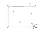
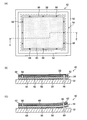
- FIG. 4 is a plan view of the laminate 6 in which the peeling start portions 26 and 30 are created.
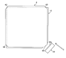
- FIG. 5 is a plan view showing a state before the knife 20 is inserted into the laminate 6 (also referred to as insertion).
- corner cut portions 6A, 6B, 6C, and 6D are provided at each corner portion of the laminate 6.
- the corner cut portions 6A to 6D are notches that are chamfered into a taper shape by a grindstone and indicate the model number of the laminated body 6. The chamfering amount and the chamfering angle are different for each model number. .
- corner cut portions 6A to 6D are provided at all corners, but there is also a laminate in which a corner cut portion is provided at at least one selected corner. 4 and 5, the corner cut portions 6A to 6D are exaggerated with respect to the size of the stacked body 6. However, the corner cut portions 6A to 6D are actually very small in size.
- the laminated body 6 is held in the horizontal direction (X-axis direction in the figure) with the back surface of the reinforcing plate 3B adsorbed and held by the table 12 as the laminated body holding means as shown in FIG. ) Is supported.
- the knife 20 is supported in the horizontal direction by the holder 14 which is a knife holding unit in FIG. 3 so that the blade edge 20 a faces the corner cut portion 6 ⁇ / b> A of the laminate 6.
- the position of the knife 20 in the height direction (Z-axis direction in the figure) is adjusted by the height adjusting device 16.
- the knife 20 and the laminated body 6 are relatively moved in the horizontal direction (X direction in the figure) by a feeding device 18 such as a ball screw device as a moving means.
- the feeding device 18 may move at least one of the knife 20 and the table 12 in the horizontal direction. In the embodiment, the knife 20 is moved.
- the insertion position of the knife 20 is the corner cut part 6A of the laminated body 6 and is set to a position overlapping in the thickness direction of the laminated body 6, and The insertion amount of the knife 20 is set to be different for each of the interfaces 24 and 28.
- the cutting edge 20a of the knife 20 is present at a position shifted in the height direction (Z-axis direction) with respect to the interface 24 between the substrate 2B and the resin layer 4B, which is the first insertion position. Therefore, first, as shown in FIG. 3A, the knife 20 is moved in the height direction, and the height of the cutting edge 20 a of the knife 20 is set to the height of the interface 24.
- the knife 20 is moved in the horizontal direction (direction of arrow B in FIG. 5) toward the corner cut portion 6A of the laminate 6, and the blade edge 20a of the knife 20 is brought into contact with the end face of the corner cut portion 6A. As shown in FIG. 3 (B), the blade edge 20a is inserted into the interface 24 by a predetermined amount.
- the knife 20 is pulled out from the corner cut portion 6A in the horizontal direction (the direction of arrow C in FIG. 5), and the blade edge 20a of the knife 20 is connected to the substrate 2A as the second insertion position as shown in FIG.
- the height of the interface 28 with the resin layer 4A is set.
- the knife 20 is moved in the horizontal direction (in the direction of arrow B in FIG. 5) toward the laminate 6, and the cutting edge 20a of the knife 20 is brought into contact with the end face of the corner cut portion 6A.
- a predetermined amount of the blade edge 20a is inserted into the interface 28.
- a peeling start portion 30 is created at the interface 28.
- the insertion amount of the knife 20 with respect to the interface 28 is set to be smaller than the insertion amount with respect to the interface 24.
- the above is the peeling start part creation method.
- the insertion amount of the knife 20 with respect to the interface 24 may be smaller than the insertion amount with respect to the interface 28.
- the laminate 6 in which the peeling start parts 26 and 30 are created is taken out from the peeling start part creating apparatus 10 and proceeds to a peeling process.
- the interfaces 24 and 28 of the laminate 6 are sequentially peeled by a peeling device.
- the laminated body 6 is bent from the corner cut portion 6A toward the corner cut portion 6C facing the corner cut portion 6A as shown by an arrow A in FIG. Then, the interface 24 having a large area of the peeling start portion 26 is peeled first from the peeling start portion 26 as a starting point. Thereby, the reinforcing plate 3B is peeled off. Thereafter, the laminate 6 is bent again from the corner cut portion 6 ⁇ / b> A toward the corner cut portion 6 ⁇ / b> C, whereby the interface 28 having a small area of the peeling start portion 30 is peeled off from the peeling start portion 30. Thereby, the reinforcing plate 3A is peeled off.
- the insertion amount of the knife 20 is preferably set to 7 mm or more, more preferably about 15 to 20 mm, depending on the size of the laminate 6.
- the knife 20 of the embodiment used in the peeling start part creating apparatus 10 can scrape at least a part of the resin layer 4B when the knife 20 is inserted into the interface 24, and when the knife 20 is inserted into the interface 28.
- the resin layer 4A has a shape that allows at least a part of the resin layer 4A to be shaved. By scraping at least part of the resin layer 4A, it is possible to suppress the substrate 2A and the reinforcing plate 3A from reattaching, and by shaving at least part of the resin layer 4B, the substrate 2B and the reinforcing plate 3B are attached again. This can be suppressed.
- the action capable of suppressing the reattachment between the substrate and the reinforcing plate will be described by taking the substrate 2A, the reinforcing plate 3A, and the resin layer 4A as an example.
- the substrate 2A and the reinforcing plate 3A are pasted via the resin layer 4A (FIG. 3A).
- the knife 20 is inserted into the interface 28, at least a part of the resin layer 4A is scraped by the knife 20 along the insertion direction (movement direction) of the knife 20, and a linear scratch is formed on the resin layer 4A. It is formed (FIG. 3D).
- the convex part higher than the surrounding resin layer 4A may be formed in the both edges of the linear crack formed in 4A of resin layers. This convex part plays the role of a spacer like shavings, and it can suppress that the board
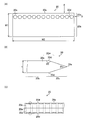
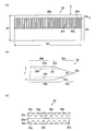
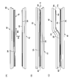
- FIGS. 6A to 6C show a knife 20 according to an embodiment.
- 6A is a plan view of the knife 20
- FIG. 6B is a side view of the knife 20 viewed from the direction of arrow D
- FIG. 6C is a front view of the knife 20 viewed from the direction of arrow E. It is.
- the knife 20 includes a main body portion 20b having a substantially constant thickness and a blade edge portion 20c tapered toward the blade edge 20a continuously with the main body portion 20b.
- the knife 20 is formed with a ridge line 20d that is a boundary between the main body portion 20b and the blade edge portion 20c.
- the ridge line 20 d extends substantially parallel to the blade edge 20 a along the width direction of the knife 20.
- the ridge line 20d includes a ridge line 20d, an area within the range of half the length of the blade edge part 20c from the ridge line 20d to the body part 20b side and 5mm from the ridge line 20d to the blade edge part 20c side. It is called.
- the knife 20 is a double-edged knife because the blade 20a of the knife 20 is located at the approximate center in the thickness direction of the main body 20b and tapers toward the blade 20a. Therefore, the ridge line 20 d exists on the first surface and the second surface of the knife 20.
- the first surface and the second surface of the knife 20 mean two surfaces having a large area in the knife 20 (hereinafter, the first surface and the second surface are collectively referred to simply as “both surfaces”).
- a plurality of through holes 20e are formed at positions that cross the ridgeline 20d.
- the through hole 20e has a substantially circular shape in plan view.
- the intersection of the circled ridge line 20 d and the through hole 20 e constitutes a protruding portion when viewed from the moving direction of the knife 20. Therefore, when the knife 20 is inserted into the interface 28, for example, the resin layer 4A can be shaved by the protruding portion at the intersection of the ridge line 20d and the through hole 20e (see FIG. 3D). Similarly, when the knife 20 is inserted into the interface 24, the resin layer 4B can be scraped by the protruding portion at the intersection of the ridge line 20d and the through hole 20e (see FIG. 3B).
- the substantially circular through hole 20e is illustrated in plan view, but may be an ellipse, a rectangle, a triangle, or a polygon.
- the size of the through holes 20e (here, the length of the ridgeline 20d) is preferably 0.1 to 5 mm, and the pitch of the plurality of through holes 20e is preferably larger than the size of the through holes 20e. Unequal pitch may be used.
- the size and pitch of the through holes 20e can be set as appropriate.
- the width W1 of the knife 20 is preferably 5 to 50 mm, the length W2 is preferably 30 to 200 mm, and the thickness t is preferably 0.05 to 0.5 mm.
- the angle ⁇ 1 of the blade edge portion 20c is preferably 20 to 30 °, and the angle ⁇ 2 formed by the main body portion 20b and the blade edge portion 20c is preferably 165 to 170 °.
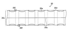
- FIG. 7 shows another embodiment of the knife 20 of the embodiment of FIGS. 6 (A) to 6 (C).
- FIG. 7 is a front view seen from the blade edge 20a as in FIG.
- the knife 20 has through holes 20e so that the plurality of through holes 20e cross the ridgeline 20d.
- a burr 20f is formed in the through hole 20e.
- the protruding directions of the burrs 20f are preferably opposite to each other.
- the resin layer can be cut by the knife 20 regardless of which side of the both sides of the knife 20 the resin layer is disposed.
- the burr 20f can be formed around the through hole 20e by punching the knife 20. Further, the through hole 20e is formed by punching from the first surface of the knife 20, and the through hole 20e is formed by punching from the second surface of the knife 20 at another position, thereby projecting on both sides of the knife 20.
- the burrs 20f whose directions are opposite to each other can be formed.
- FIG. 8A to 8C show a knife 20 according to another embodiment.
- 8A is a plan view of the knife 20
- FIG. 8B is a side view of the knife 20 viewed from the direction of arrow F
- FIG. 8C is a front view of the knife 20 viewed from the direction of arrow G.
- the knife 20 is similar to FIGS. 6A to 6C in that the main body portion 20b, the blade edge portion 20c, and the ridge line 20d that is the boundary between the main body portion 20b and the blade edge portion 20c.
- the blade edge 20a is a double-edged knife located at a substantially central portion in the thickness direction of the main body portion 20b.
- peaks 20g and valleys 20h extending in a direction substantially perpendicular to the cutting edge 20a are alternately formed on both surfaces of the main body 20b of the knife 20 of the embodiment. Therefore, as shown in FIG. 8A, the ridge line 20d, which is the boundary between the main body portion 20b and the blade edge portion 20c, is wavy in a plan view. Wavy means a case where a certain shape undulates at a certain interval, and does not mean that the shape is a wave itself. Therefore, the peak part 20g and the valley part 20h may be V-shaped, U-shaped, or the like when viewed from the front.
- the position of the ridge line 20d between the main body portion 20b and the blade edge portion 20c in the peak portion 20g in the side view and the position of the ridge line 20d between the main body portion 20b and the blade edge portion 20c in the valley portion 20h are as follows.
- the thickness direction of the knife 20 and the length direction (direction of W1) are different.
- the blade edge portion 20c is formed in a wave shape by a peak portion 20g and a valley portion 20h in a front view.
- the ridge line 20d surrounded by a circle constitutes a protruding portion when viewed from the moving direction of the knife 20. Therefore, when the knife 20 is inserted into the interface 28, the resin layer 4A can be cut by the ridgeline 20d that is the protruding portion (see FIG. 3D). Similarly, when the knife 20 is inserted into the interface 24, the resin layer 4B can be shaved by the ridgeline 20d that is the protruding portion (see FIG. 3B).
- the knife 20 shown in FIG. 8 can be manufactured by, for example, polishing a flat plate in which crests and troughs are alternately formed in a direction in which crests and troughs extend to form a cutting edge. .
- the material of the knife 20, the width W1, the length W2, the thickness t, the angle ⁇ 1 of the blade edge portion 20c, and the angle ⁇ 2 formed by the main body portion 20b and the blade edge portion 20c are the same material and size as the knife 20 of FIG. Can be
- FIGS. 9A to 9C show a knife 20 according to another embodiment.
- 9A is a plan view of the knife 20
- FIG. 9B is a side view of the knife 20 viewed from the direction of arrow H
- FIG. 9C is a front view of the knife 20 viewed from the direction of arrow I.
- the knife 20 includes a main body portion 20b, a blade edge portion 20c, and a ridge line 20d that is a boundary between the main body portion 20b and the blade edge portion 20c, as in FIG. 6B.
- the blade edge 20a is a double-edged knife located at a substantially central portion in the thickness direction of the main body 20b.
- particles 20k are attached to the ridge line portion 20m including the ridge line 20d on both surfaces of the knife 20. Since the particles 20k attached to both surfaces of the knife 20 constitute a protrusion, the resin layer 4A can be scraped by the particles 20k when the knife 20 is inserted into the interface 28 (see FIG. 3D). Similarly, when the knife 20 is inserted into the interface 24, the resin layer 4B can be scraped by the particles 20k (see FIG. 3B).
- the particles 20k for example, particles of a material such as diamond, glass, or metal are preferably used.
- the particle diameter of the particles 20k is preferably 0.1 to 100 ⁇ m, and the density is preferably 1 to 1000 particles / cm 2 .
- electrodeposition by adhesion or plating can be used.
- the material of the knife 20 the width W1, the length W2, the thickness t, the angle ⁇ 1 of the blade edge portion 20c, and the angle ⁇ 2 formed by the main body portion 20b and the blade edge portion 20c are the knives shown in FIGS.
- the same material and size as 20 can be used.
- the knife 20 shown in FIGS. 6 (A) to (C) to FIGS. 9 (A) to (C) has an example of having a straight blade edge 20a in plan view
- the present invention is not limited to this.
- the cutting edge 20a may be wavy or saw-toothed in plan view.
- FIGS. 10A to 10C are plan views showing a method for creating a peeling start portion in a laminate
- FIGS. 11A to 11C are side views showing a method for creating a peeling start portion in a laminate.
- FIG. 10A and 11A the knife 20 is moved in the height direction so as to face the corner cut portion 6A of the laminated body 6, and the cutting edge 20a of the knife 20 The height is set to the height of the interface 24 between the substrate 2B and the resin layer 4B.
- the knife 20 is formed with fifteen through-holes 20e with a diameter of 2 mm at positions 4 mm across the ridgeline 20d. The fifteen through holes 20e are arranged substantially parallel to the cutting edge 20a.
- FIGS. 10A to 10C For ease of understanding, only the resin layer 4B of the laminate 6 is shown in FIGS. 10A to 10C, and in FIGS. 11A to 11C, the substrate 2B, the reinforcing plate 3B, Only the resin layer 4B is displayed.
- the knife 20 is inserted into the interface 24 with a predetermined insertion amount along the direction of arrow J (arrow L in FIG. 11B). Since the knife 20 is a double-edged knife, the substrate 2B and the reinforcing plate 3B including the resin layer 4B are pushed and expanded in the traveling direction of the knife 20 (in FIG. 11B, the substrate 2B is an arrow M). The reinforcing plate 3B including the resin layer 4B is in the direction of arrow N), and the knife 20 moves.
- the force in the direction opposite to the arrows M and N acts due to the rigidity of the substrate 2B and the reinforcing plate 3B, and the ridge line portion 20m including the ridge line 20d of the knife 20 is applied to the resin layer 4B. Pressed locally. Since the intersection of the through-hole 20e and the ridgeline 20d constitutes a protrusion, the resin layer 4B can be easily scraped by this protrusion.
- FIG. 10B when the resin layer 4B is shaved along the moving direction of the knife 20 by the knife 20, a linear scratch 32 corresponding to the moving direction of the knife 20 is formed on the surface of the resin layer 4B. Is formed. Since the scratch 32 is formed while cutting the resin layer 4B with the knife 20, the shavings 34 adhere to the substrate 2B and the resin layer 4B as shown in FIG. Moreover, the convex part (not shown) higher than the surrounding resin layer 4B is formed in the linear both edges of the crack 32.
- FIG. 10B when the resin layer 4B is shaved along the moving direction of the knife 20 by the knife 20, a linear scratch 32 corresponding to the moving direction of the knife 20 is formed on the surface of the resin layer 4B. Is formed. Since the scratch 32 is formed while cutting the resin layer 4B with the knife 20, the shavings 34 adhere to the substrate 2B and the resin layer 4B as shown in FIG. Moreover, the convex part (not shown) higher than the surrounding resin layer 4B is formed in the linear both edges of
- the knife 20 is pulled out in the direction of the arrow K (arrow P in FIG. 11) opposite to the direction of the arrow J (arrow L in FIG. 11). That is, the knife 20 is pulled out so as to follow the trajectory of the advanced knife 20 in the reverse direction. As shown in FIG. 10C, a peeling start portion 26 corresponding to the insertion amount of the knife 20 is formed in the vicinity of the corner cut portion 6A.
- the shavings 34 of the resin layer 4B exist at the interface 24 between the substrate 2B and the resin layer 4B, the shavings 34 function as a spacer, and the substrate 2B and the resin layer 4B. And reattachment can be suppressed. Further, as shown in FIG. 10C, when convex portions (not shown) on both edges of the scratch 32 are formed, it functions as a spacer.
- FIGS. 12A to 12C are plan views showing a method for creating a peeling start portion in a laminate.
- the knife 20 is moved in the height direction and set to a position facing the corner cut portion 6A of the laminate 6.
- the height of the cutting edge 20a of the knife 20 is set to the height of the interface 24 between the substrate 2B and the resin layer 4B (see FIG. 11A).
- the knife 20 is inserted into the interface 24 along the direction of the arrow Q with a predetermined insertion amount. Scratches 32 are formed in the resin layer 4 ⁇ / b> B along the moving direction of the knife 20.
- the knife 20 in the embodiment of FIGS. 12A to 12C has a through hole 20e as compared with the knife 20 in the embodiment of FIGS. 10A to 10C and FIGS. 11A to 11C.
- the number is small. Accordingly, the number of scratches 32 formed in the resin layer 4B of the embodiment of FIGS. 12A to 12C is the same as that of the embodiments of FIGS. 10A to 10C and FIGS. 11A to 11C. This is less than the number of scratches 32 formed in the resin layer 4B.
- the through hole 20e may not pass through the corner cut portion 6A.
- FIG. 12 (C) it is pulled out in the direction of arrow R (left direction in the drawing), not in the direction opposite to the direction of arrow Q in which the knife 20 is inserted. That is, the knife 20 is pulled out so as not to follow the trajectory of the advanced knife 20 in reverse.
- New scratches 32 can be formed in the resin layer 4B. Therefore, even if the knife 20 has a small number of through holes 20e, the scratch 32 having the same area as that of the knife 20 having many through holes 20e can be formed by controlling the movement direction of the knife 20.
- the direction of movement of the knife 20 is not limited to the embodiment, and is appropriately set depending on the size and number of the through holes 20e.
- the knife 20 that has few through holes 20e and is inexpensive to manufacture.
- 6 (A) to 6 (C) to 9 (A) to 9 (C) exemplify the double-edged knife 20, but the present invention is not limited to this, and a single-edged knife can be used.
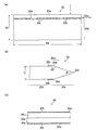
- FIGS. 13A and 13B are explanatory views showing an embodiment of a single-edged knife.
- the knife 20 includes a main body portion 20b having a substantially constant thickness and a cutting edge portion 20c tapered toward the cutting edge 20a continuously with the main body portion 20b in a side view.
- the cutting edge 20a of the knife 20 is positioned on either the first surface or the second surface in the thickness direction of the main body portion 20b, so that the knife 20 is a single-edged knife. It is. Therefore, the ridge line 20d exists only on one surface of the first surface and the second surface of the knife 20, and the surface on which the ridge line 20d does not exist is a flat surface.
- the knife 20 of the embodiment has a plurality of through-holes 20e that cross the ridgeline 20d as a shape that can cut the resin layer as the adsorption layer.
- the plurality of through holes 20e are arranged substantially parallel to the blade edge 20a.
- FIG. 13B is a side view showing a state in which the knife 20 is inserted into the laminate 6.
- the substrate 2B, the reinforcing plate 3B, and the resin layer 4B are shown.
- the knife 20 is inserted into the interface between the substrate 2B and the resin layer 4B along the direction of the arrow S with a predetermined insertion amount. Since the knife 20 is a single-edged knife, the knife 20 moves while pushing the reinforcing plate 3B including the resin layer 4B in the direction of the arrow T with respect to the traveling direction of the knife 20. When the knife 20 is moved along the interface 24, a force in the direction opposite to the arrow T acts due to the rigidity of the substrate 2B and the reinforcing plate 3B, and the ridge line portion 20m including the ridge line 20d of the knife 20 is locally applied to the resin layer 4B. Pressed. Since the intersection of the through-hole 20e and the ridgeline 20d constitutes a protrusion, the resin layer 4B can be easily scraped by this protrusion.
- the ridge line 20d is formed on only one surface, the influence on the substrate 2B can be reduced.
- the ridge line portion 20m of the knife 20 is formed on the resin layer 4B as shown in FIGS. 13A and 13B.
- the knife 20 is disposed at the opposite position.
- the ridge line portion 20m of the knife 20 is disposed at a position facing the resin layer 4A.
- the knife 20 may be turned upside down so that the ridge 20m of the knife 20 faces the respective resin layers 4B and 4A. preferable.
- the ridgeline part 20m can be arrange
- the burr When a burr (not shown) is formed on the knife 20 having the through hole 20e, the burr may be formed in a direction protruding from the surface having the ridgeline 20d.
- FIGS. 13A and 13B the case where the through-hole 20e is formed in the ridge line 20d with respect to the single-edged knife 20 has been described, but the ridge line 20d is waved as shown in FIGS. 8A to 8C.
- the particle 20k can be provided on the ridge 20m.
- the width W1 and the length W2 can be the same as those shown in FIGS.
- the thickness t is preferably 0.05 to 0.5 mm.
- the angle ⁇ 1 of the blade edge portion 20c is preferably 10 to 15 °, and the angle ⁇ 2 formed by the main body portion 20b and the blade edge portion 20c is preferably 165 to 170 °.
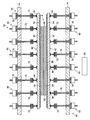
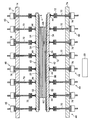
- FIG. 14 is a longitudinal sectional view showing the configuration of the peeling device 40 of the embodiment, and FIG. 15 is a peeling unit 42 schematically showing the arrangement positions of the plurality of movable bodies 44 with respect to the peeling unit 42 of the peeling device 40.
- FIG. 14 corresponds to a cross-sectional view taken along the line DD in FIG. 15.
- the stacked body 6 is indicated by a solid line.
- the peeling device 40 includes a pair of movable devices 46 and 46 that are arranged vertically with the laminate 6 interposed therebetween. Since the movable devices 46 and 46 have the same configuration, the movable device 46 disposed on the lower side of FIG. 14 will be described here, and the description of the movable device 46 disposed on the upper side will be omitted by attaching the same reference numerals. .
- the movable device 46 includes a plurality of movable bodies 44, a plurality of drive devices 48 that move the movable body 44 up and down for each movable body 44, a controller 50 that controls the drive device 48 for each drive device 48, and the like.
- the peeling unit 42 holds the reinforcing plate 3B by vacuum suction so as to bend and deform the reinforcing plate 3B.
- vacuum suction instead of vacuum suction, electrostatic suction or magnetic suction may be used.
- FIG. 16A is a plan view of the peeling unit 42
- FIG. 16B is an enlarged longitudinal sectional view of the peeling unit 42 taken along line EE of FIG. 16A.
- FIG. 16C shows that a suction portion 54 constituting the peeling unit 42 is detachably attached to the rectangular plate-like flexible plate 52 constituting the peeling unit 42 via a double-sided adhesive tape 56.
- FIG. 6 is an enlarged vertical cross-sectional view of the peeling unit 42 showing that it has been done.
- the peeling unit 42 is configured by attaching the adsorbing portion 54 to the flexible plate 52 through the double-sided adhesive tape 56 in a detachable manner as described above.
- the adsorption unit 54 includes a flexible plate 58 that is thinner than the flexible plate 52.
- the lower surface of the flexible plate 58 is detachably attached to the upper surface of the flexible plate 52 via a double-sided adhesive tape 56.
- the adsorbing portion 54 is provided with a rectangular air permeable sheet 60 that adsorbs and holds the inner surface of the reinforcing plate 3B of the laminate 6.
- the thickness of the breathable sheet 60 is 2 mm or less, preferably 1 mm or less for the purpose of reducing the tensile stress generated in the reinforcing plate 3B at the time of peeling, and in the embodiment, the thickness of 0.5 mm is used.
- the adsorbing part 54 is provided with a seal frame member 62 that surrounds the air-permeable sheet 60 and that contacts the outer peripheral surface of the reinforcing plate 3B.
- the seal frame member 62 and the breathable sheet 60 are bonded to the upper surface of the flexible plate 58 via a double-sided adhesive tape 64.
- the seal frame member 62 is a closed-cell sponge having a Shore E hardness of 20 degrees or more and 50 degrees or less, and the thickness thereof is configured to be 0.3 mm to 0.5 mm thicker than the thickness of the breathable sheet 60. Has been.
- a frame-shaped groove 66 is provided between the air-permeable sheet 60 and the seal frame member 62.
- a plurality of through holes 68 are opened in the flexible plate 52, and one end of each of these through holes 68 is communicated with the groove 66, and the other end is connected to an intake source via a suction pipe (not shown). (For example, a vacuum pump).
- the air in the suction pipe, the through hole 68, and the groove 66 is sucked, whereby the inner surface of the reinforcing plate 3B of the laminated body 6 is vacuum-sucked and held on the breathable sheet 60. . Further, since the outer peripheral surface of the reinforcing plate 3B is in contact with the seal frame member 62 in a pressed state, the sealing performance of the adsorption space surrounded by the seal frame member 62 is improved.
- the flexible plate 52 has higher bending rigidity than the flexible plate 58, the air permeable sheet 60, and the seal frame member 62, and the bending rigidity of the flexible plate 52 dominates the bending rigidity of the peeling unit 42.
- the bending rigidity per unit width (1 mm) of the peeling unit 42 is preferably 1000 to 40000 N ⁇ mm 2 / mm. For example, in a portion where the width of the peeling unit 42 is 100 mm, the bending rigidity is 100,000 to 4000000 N ⁇ mm 2 .
- the bending rigidity of the peeling unit 42 By setting the bending rigidity of the peeling unit 42 to 1000 N ⁇ mm 2 / mm or more, it is possible to prevent the reinforcing plate 3B from being bent and held by the peeling unit 42 from being bent. Further, by setting the bending rigidity of the peeling unit 42 to 40000 N ⁇ mm 2 / mm or less, the reinforcing plate 3B sucked and held by the peeling unit 42
- the flexible plates 52 and 58 are resin members, for example, resin members such as polycarbonate resin, polyvinyl chloride (PVC) resin, acrylic resin, and polyacetal (POM) resin.
- resin members such as polycarbonate resin, polyvinyl chloride (PVC) resin, acrylic resin, and polyacetal (POM) resin.
- a plurality of disk-shaped movable bodies 44 shown in FIG. 14 are fixed to the lower surface of the flexible plate 52 in a grid pattern as shown in FIG. These movable bodies 44 are fixed to the flexible plate 52 by fastening members such as bolts, but may be bonded and fixed instead of the bolts. These movable bodies 44 are moved up and down independently by a drive device 48 that is driven and controlled by the controller 50.
- the controller 50 controls the driving device 48 and is located on the corner cut portion 6C side in the peeling progress direction indicated by the arrow U from the movable body 44 located on the corner cut portion 6A side of the laminate 6 in FIG.
- the movable body 44 is sequentially moved downward.
- the interface 24 of the laminate 6 is peeled off from the peeling start portion 26 (see FIG. 4) as shown in the longitudinal sectional view of FIG.
- the laminate 6 shown in FIGS. 14 and 17 is the laminate 6 in which the peeling start portions 26 and 30 are created by the peeling start portion creating method described in FIGS. 3 (A) to 3 (C).
- the drive device 48 is composed of, for example, a rotary servo motor and a ball screw mechanism.
- the rotational motion of the servo motor is converted into linear motion in the ball screw mechanism and transmitted to the rod 70 of the ball screw mechanism.
- a movable body 44 is provided at the tip of the rod 70 via a ball joint 72. Thereby, the movable body 44 can be tilted following the bending deformation of the peeling unit 42 as shown in FIG. Therefore, the peeling unit 42 can be bent and deformed from the corner cut portion 6A toward the corner cut portion 6C without applying an excessive force to the peeling unit 42.
- the drive device 48 is not limited to a rotary servo motor and a ball screw mechanism, and may be a linear servo motor or a fluid pressure cylinder (for example, a pneumatic cylinder).
- the plurality of driving devices 48 be attached to a frame 74 that can be raised and lowered via a cushion member 76.
- the cushion member 76 is elastically deformed so as to follow the bending deformation of the peeling unit 42. As a result, the rod 70 tilts with respect to the frame 74.
- the frame 74 is moved downward by a drive unit (not shown) when the peeled reinforcing plate 3B is removed from the peeling unit 42.
- the controller 50 is configured as a computer including a recording medium such as a CPU (Central Processing Unit), a ROM (Read Only Memory), and a RAM (Random Access Memory).
- the controller 50 controls the plurality of driving devices 48 for each of the driving devices 48 by causing the CPU to execute the program recorded on the recording medium, thereby controlling the vertical movement of the plurality of movable bodies 44.
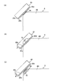
- FIG. 18 (A) to (C) to FIG. 19 (A) to (C) show the peeling start portion 26 on the corner cut portion 6A by the peeling start portion creation method described in FIG. 3 (A) to (C).
- the peeling method of the laminated body 6 in which 30 was produced is shown. That is, in the drawing, a peeling method for peeling the reinforcing plates 3A and 3B of the laminate 6 is shown in time series.
- the panel PA is a product panel in which the substrate 2A and the substrate 2B excluding the reinforcing plates 3A and 3B are bonded via the functional layer 7.
- FIG. 18A is a side view of the peeling device 40 in which the laminate 6 is placed on the lower peeling unit 42 by the operation indicated by the arrows V and W of the conveying device 80.
- the lower peeling unit 42 and the upper peeling unit 42 are relatively sufficiently retracted so that the transfer device 80 is inserted between the lower peeling unit 42 and the upper peeling unit 42. It is moved in advance to the position.
- the lower peeling unit 42 holds the reinforcing plate 3 ⁇ / b> B of the laminated body 6 by vacuum suction. That is, FIG. 18A shows an adsorption process in which the reinforcing plate 3B is adsorbed and held by the lower peeling unit 42.
- FIG. 18B shows an adsorption process in which the reinforcing plate 3A is adsorbed and held by the upper peeling unit 42.
- the support part that supports the substrate 2 is not limited to the peeling unit 42, and may be any member that can detachably support the substrate 2.
- the peeling unit 42 since the substrate 2 and the reinforcing plate 3 can be simultaneously bent and peeled by using the peeling unit 42 as the support portion, the peeling force can be increased as compared with a mode in which only the substrate 2 or the reinforcing plate 3 is bent. There is an advantage that can be reduced.
- FIG. 18C shows the interface 24 of the laminated body 6 while bending and deforming the lower peeling unit 42 downward from the corner cut part 6 ⁇ / b> A of the laminated body 6 toward the corner cut part 6 ⁇ / b> C. It is the side view which showed the state which peels from the peeling start part 26 (refer FIG. 4). That is, in the plurality of movable bodies 44 of the lower peeling unit 42 shown in FIG. 17, the movable bodies 44 located on the corner cut portion 6C side are sequentially moved from the movable bodies 44 located on the corner cut portion 6A side of the laminate 6. The interface 24 is peeled off by moving downward.
- the movable bodies 44 located on the corner cut portion 6C side from the movable bodies 44 located on the corner cut portion 6A side of the laminate 6 are changed.
- the interface 24 may be peeled off by sequentially moving up. Thereby, a peeling force can be made small compared with the form which curves only the reinforcement board 3B.
- FIG. 19A is a side view of the peeling apparatus 40 in a state where the interface 24 is completely peeled off.
- the peeled reinforcing plate 3B is vacuum-sucked and held by the lower peeling unit 42
- the laminated body 6 a laminated body including the reinforcing plate 3A and the panel PA
- the reinforcing plate 3B is the upper peeling unit 42. Is held by vacuum suction.
- the lower peeling unit 42 and the upper peeling unit 42 are relatively sufficiently retracted so that the conveying device 80 shown in FIG. 18A is inserted between the upper and lower peeling units 42. Moved to position.
- the vacuum suction of the lower peeling unit 42 is released.
- the reinforcing plate 3B is sucked and held by the suction pad 78 of the transport device 80 via the resin layer 4B.
- the reinforcing plate 3B is unloaded from the peeling device 40 by the operation of the transfer device 80 (see FIG. 18A) indicated by arrows AA and BB in FIG.
- FIG. 19B is a side view in which the laminate 6 excluding the reinforcing plate 3B is vacuum-sucked and held by the lower peeling unit 42 and the upper peeling unit 42. That is, the lower peeling unit 42 and the upper peeling unit 42 are moved in a relatively approaching direction, and the substrate 2B is held by vacuum suction on the lower peeling unit 42.
- FIG. 19C shows the interface 28 of the laminate 6 with the peeling start portion 30 (FIG. 19) while the upper peeling unit 42 is bent upwardly from the corner cut portion 6A to the corner cut portion 6C of the laminate 6.
- 4 is a side view showing a state of peeling from the starting point. That is, in the plurality of movable bodies 44 of the upper peeling unit 42 shown in FIG. 17, the movable bodies 44 located on the corner cut portion 6C side are sequentially raised from the movable bodies 44 located on the corner cut portion 6A side of the laminate 6.
- the interface 28 is peeled off by moving.
- the movable body 44 located on the corner cut portion 6 ⁇ / b> C side from the movable body 44 located on the corner cut portion 6 ⁇ / b> A side of the laminate 6. May be sequentially moved downward to peel the interface 28. Thereby, a peeling force can be made small compared with the form which curves only reinforcement board 3A.
- the reinforcing plate 3A completely peeled from the panel P is taken out from the upper peeling unit 42, and the panel PA is taken out from the lower peeling unit 42.
- the above is the peeling method of the laminated body 6 in which the peeling start parts 26 and 30 were created in the corner cut part 6A.
Landscapes
- Physics & Mathematics (AREA)
- Engineering & Computer Science (AREA)
- Ceramic Engineering (AREA)
- Nonlinear Science (AREA)
- Chemical & Material Sciences (AREA)
- General Physics & Mathematics (AREA)
- Crystallography & Structural Chemistry (AREA)
- Optics & Photonics (AREA)
- Mathematical Physics (AREA)
- Theoretical Computer Science (AREA)
- Manufacturing & Machinery (AREA)
- Mechanical Engineering (AREA)
- Electroluminescent Light Sources (AREA)
- Laminated Bodies (AREA)
- Folding Of Thin Sheet-Like Materials, Special Discharging Devices, And Others (AREA)
- Devices For Indicating Variable Information By Combining Individual Elements (AREA)
Abstract
Description
電子デバイスは、ガラス製、樹脂製、金属製等の基板の表面に電子デバイス用の機能層(LCDであれば、薄膜トランジスタ(TFT)、カラーフィルタ(CF))を形成することにより製造される。
図1は、積層体1の一例を示した要部拡大側面図である。
第1の基板である基板2は、その表面2aに機能層が形成される。基板2としては、ガラス基板、セラミックス基板、樹脂基板、金属基板、半導体基板を例示できる。例示されたこれらの基板のなかでも、ガラス基板は、耐薬品性、耐透湿性に優れ、かつ、線膨張係数が小さいので、電子デバイス用の基板2として好適である。また、線膨張係数が小さくなるに従い、高温下で形成される機能層のパターンが冷却時にずれ難くなる利点もガラス基板にはある。
第2の基板である補強板3としては、ガラス基板、セラミックス基板、樹脂基板、金属基板、半導体基板を例示できる。
吸着層である樹脂層4は、樹脂層4と補強板3との間で剥離するのを防止するため、樹脂層4と補強板3との間の結合力が、樹脂層4と基板2との間の結合力よりも高く設定される。これにより、積層体1を剥離する工程では、樹脂層4と基板2との間で剥離が行われる。
機能層形成工程を経ることにより積層体1の基板2の表面2aには、機能層が形成される。機能層の形成方法としては、CVD(Chemical Vapor Deposition)法、PVD(Physical Vapor Deposition)法等の蒸着法、スパッタ法が用いられる。機能層は、フォトリソグラフィ法、エッチング法によって所定のパターンに形成される。
図3(A)~(E)は、剥離開始部作成工程にて使用される剥離開始部作成装置10の要部構成を示した説明図であり、図3(A)は、積層体6とナイフ20(剥離刃とも称される)との位置関係を示した説明図、図3(B)は、ナイフ20によって基板2Bと樹脂層4Bとの界面24に剥離開始部26を作成する説明図、図3(C)は、基板2Aと樹脂層4Aとの界面28に剥離開始部30を作成する直前状態を示した説明図、図3(D)は、ナイフ20によって界面28に剥離開始部30を作成する説明図、図3(E)は、剥離開始部26、30が作成された積層体6の説明図である。また、図4は、剥離開始部26、30が作成された積層体6の平面図である。図5は、積層体6にナイフ20を挿入(刺入ともいう)する前の状態を示した平面図である。
剥離開始部作成装置10による剥離開始部作成方法によれば、ナイフ20の挿入位置を、積層体6のコーナーカット部6Aであって、積層体6の厚さ方向において重なる位置に設定し、かつナイフ20の挿入量を、界面24、28ごとに異なるように設定している。
本発明に係る積層体の剥離開始部作成方法、及び剥離開始部作成装置の特徴について説明する。本発明の特徴は、特定の形状を有するナイフ20による剥離開始部作成方法にあり、その点について以下に述べる。
吸着層である樹脂層4A、4Bを削ることができるナイフ20の形状について説明する。図6(A)~(C)は一実施形態のナイフ20を示している。図6(A)はナイフ20の平面図であり、図6(B)はナイフ20を矢印Dの方向から見た側面図であり、図6(C)は矢印Eの方向から見た正面図である。図6(B)の如く、側面視でナイフ20は、略一定厚さの本体部20bと、この本体部20bと連続して刃先20aに向かって先細りの刃先部20cを備えている。ナイフ20には、本体部20bと刃先部20cの境界である稜線20dが形成されている。稜線20dはナイフ20の幅方向に沿って刃先20aと略平行に延びている。なお、実施形態において、稜線20dを含み、稜線20dから本体部20bの側に5mm、及び稜線20dから刃先部20cの側に刃先部20cの長さの半分の範囲内の領域を稜線部20mと称している。
図14は、実施形態の剥離装置40の構成を示した縦断面図であり、図15は、剥離装置40の剥離ユニット42に対する複数の可動体44の配置位置を模式的に示した剥離ユニット42の平面図である。なお、図14は図15のD-D線に沿う断面図に相当し、また、図15においては積層体6を実線で示している。
図16(A)は、剥離ユニット42の平面図であり、図16(B)は、図16(A)のE-E線に沿う剥離ユニット42の拡大縦断面図である。また、図16(C)は、剥離ユニット42を構成する矩形の板状の可撓性板52に対して、剥離ユニット42を構成する吸着部54が両面接着テープ56を介して着脱自在に備えられたことを示す剥離ユニット42の拡大縦断面図である。
可撓性板52の下面には、図14に示した円盤状の複数の可動体44が、図15の如く碁盤目状に固定される。これらの可動体44は、可撓性板52にボルト等の締結部材によって固定されるが、ボルトに代えて接着固定されてもよい。これらの可動体44は、コントローラ50によって駆動制御された駆動装置48によって、独立して昇降移動される。
1A…第1の積層体
1B…第2の積層体
2,2A,2B…基板(第1の基板)
3,3A,3B…補強板(第2の基板)
4,4A,4B…樹脂層(吸着層)
6…積層体
10…剥離開始部作成装置
12…テーブル(積層体保持手段)
14…ホルダ(ナイフ保持手段)
18…送り装置(移動手段)
20…ナイフ
20b…本体部
20c…刃先部
20d…稜線
20e…貫通孔
20f…バリ
20g…山部
20h…谷部
20k…粒子
20m…稜線部
26…剥離開始部
30…剥離開始部
40…剥離装置
Claims (18)
- 第1の基板と第2の基板とが吸着層を介して剥離可能に貼り付けられた積層体に対して、前記第1の基板と前記吸着層との界面に前記積層体の端面からナイフを所定量挿入して前記界面に剥離開始部を作成する積層体の剥離開始部作成方法において、
前記ナイフは、本体部と、前記本体部と連続して側面視で先細りの刃先部と、前記本体部と前記刃先部との境界である稜線とを含み、
前記稜線を含む稜線部により前記吸着層の少なくとも一部を削る積層体の剥離開始部作成方法。 - 前記稜線部は、前記稜線を横切る位置に複数の貫通孔を有する形状を有する請求項1に記載の積層体の剥離開始部作成方法。
- 前記複数の貫通孔の少なくとも一つは、バリを有する貫通孔である請求項2に記載の積層体の剥離開始部作成方法。
- 前記複数の貫通孔の少なくとも二つは、バリを有する貫通孔であり、二つの前記バリの突出方向は互いに反対方向である請求項2に記載の積層体の剥離開始部作成方法。
- 前記稜線部は、前記ナイフの刃先から見て、山部と谷部とが交互に配置された波状の稜線を有する形状を有する請求項1に記載の積層体の剥離開始部作成方法。
- 前記稜線部は、粒子の配置された形状を有する請求項1に記載の積層体の剥離開始部作成方法。
- 第1の基板と第2の基板とが吸着層を介して剥離可能に貼り付けられた積層体を保持する積層体保持手段と、
ナイフを保持するナイフ保持手段と、
前記積層体保持手段及び前記ナイフ保持手段を相対的に移動させることにより、前記第1の基板と前記吸着層との界面に前記積層体の端面から前記ナイフを所定量挿入させる移動手段と、
を備えた剥離開始部作成装置であって、
前記ナイフは、本体部と、前記本体部と連続し先細りの刃先部と、前記本体部と前記刃先部との境界である稜線とを含み、前記稜線を含む稜線部は前記吸着層の少なくとも一部を削ることができる形状を有する剥離開始部作成装置。 - 前記形状は、前記稜線を横切る位置に設けられた複数の貫通孔である請求項7に記載の剥離開始部作成装置。
- 前記複数の貫通孔の少なくとも一つは、バリを有する貫通孔である請求項8に記載の剥離開始部作成装置。
- 前記複数の貫通孔の少なくとも二つは、バリを有する貫通孔であり、二つの前記バリの突出方向は互いに反対方向である請求項8に記載の剥離開始部作成装置。
- 前記形状は、前記ナイフの刃先から見て、山部と谷部とが交互に配置された波状の稜線を有する形状である請求項7に記載の剥離開始部作成装置。
- 前記形状は、前記稜線部に配置された粒子を有する形状である請求項7に記載の剥離開始部作成装置。
- 第1の基板と第2の基板とが吸着層を介して剥離可能に貼り付けられた積層体における、前記第1の基板の表面に機能層を形成する機能層形成工程と、前記機能層が形成された前記第1の基板を前記第2の基板から剥離する剥離工程とを有する電子デバイスの製造方法において、
前記剥離工程は、前記第1の基板と前記吸着層との界面に前記積層体の端面からナイフを所定量挿入して前記界面に剥離開始部を作成する剥離開始部作成工程と、前記剥離開始部を起点として前記界面を剥離する剥離工程と、を有し、
前記ナイフは、本体部と、前記本体部と連続して側面視で先細りの刃先部と、前記本体部と前記刃先部との境界である稜線とを含み、前記稜線を含む稜線部により前記吸着層の少なくとも一部を削る電子デバイスの製造方法。 - 前記稜線部は、前記稜線を横切る位置に複数の貫通孔を有する形状である請求項13に記載の電子デバイスの製造方法。
- 前記複数の貫通孔の少なくとも一つは、バリを有する貫通孔である請求項14に記載の電子デバイスの製造方法。
- 前記複数の貫通孔の少なくとも二つは、バリを有する貫通孔であり、二つの前記バリの突出方向は互いに反対方向である請求項14に記載の電子デバイスの製造方法。
- 前記稜線部は、前記ナイフの刃先から見て、山部と谷部とが交互に配置された波状の稜線を有する形状である請求項13に記載の電子デバイスの製造方法。
- 前記稜線部は、粒子の配置された形状を有する請求項13に記載の電子デバイスの製造方法。
Priority Applications (4)
| Application Number | Priority Date | Filing Date | Title |
|---|---|---|---|
| JP2016566089A JP6547760B2 (ja) | 2014-12-26 | 2015-12-07 | 積層体の剥離開始部作成方法、及び剥離開始部作成装置並びに電子デバイスの製造方法 |
| KR1020177017088A KR102437466B1 (ko) | 2014-12-26 | 2015-12-07 | 적층체의 박리 개시부 형성 방법, 및 박리 개시부 형성 장치 그리고 전자 디바이스의 제조 방법 |
| CN201580068254.XA CN107000953B (zh) | 2014-12-26 | 2015-12-07 | 剥离开始部制作方法和制作装置及电子器件的制造方法 |
| US15/616,251 US10173408B2 (en) | 2014-12-26 | 2017-06-07 | Method for creating separation start portion for layered bodies, device for creating separation start portion, and electronic device manufacturing method |
Applications Claiming Priority (2)
| Application Number | Priority Date | Filing Date | Title |
|---|---|---|---|
| JP2014-263880 | 2014-12-26 | ||
| JP2014263880 | 2014-12-26 |
Related Child Applications (1)
| Application Number | Title | Priority Date | Filing Date |
|---|---|---|---|
| US15/616,251 Continuation US10173408B2 (en) | 2014-12-26 | 2017-06-07 | Method for creating separation start portion for layered bodies, device for creating separation start portion, and electronic device manufacturing method |
Publications (1)
| Publication Number | Publication Date |
|---|---|
| WO2016104122A1 true WO2016104122A1 (ja) | 2016-06-30 |
Family
ID=56150152
Family Applications (1)
| Application Number | Title | Priority Date | Filing Date |
|---|---|---|---|
| PCT/JP2015/084272 Ceased WO2016104122A1 (ja) | 2014-12-26 | 2015-12-07 | 積層体の剥離開始部作成方法、及び剥離開始部作成装置並びに電子デバイスの製造方法 |
Country Status (6)
| Country | Link |
|---|---|
| US (1) | US10173408B2 (ja) |
| JP (1) | JP6547760B2 (ja) |
| KR (1) | KR102437466B1 (ja) |
| CN (1) | CN107000953B (ja) |
| TW (1) | TWI680060B (ja) |
| WO (1) | WO2016104122A1 (ja) |
Cited By (1)
| Publication number | Priority date | Publication date | Assignee | Title |
|---|---|---|---|---|
| JP2020178058A (ja) * | 2019-04-19 | 2020-10-29 | ハイソル株式会社 | 層状物質劈開方法 |
Families Citing this family (9)
| Publication number | Priority date | Publication date | Assignee | Title |
|---|---|---|---|---|
| CN107406294A (zh) * | 2015-01-06 | 2017-11-28 | 康宁股份有限公司 | 用于加工挠性玻璃板的玻璃载体组件和方法 |
| KR102570870B1 (ko) * | 2018-07-06 | 2023-08-28 | 삼성디스플레이 주식회사 | 합착 장치 및 이를 이용한 표시장치의 합착 방법 |
| CN109624426A (zh) * | 2018-11-14 | 2019-04-16 | 江门市艾加得电子有限公司 | 一种保护膜及其离型层剥离方法 |
| JP6916223B2 (ja) * | 2019-01-30 | 2021-08-11 | 日機装株式会社 | 剥離装置 |
| JP7262903B2 (ja) * | 2019-08-26 | 2023-04-24 | 株式会社ディスコ | キャリア板の除去方法 |
| KR102364971B1 (ko) * | 2021-08-10 | 2022-02-21 | 주식회사 원광에스앤티 | 태양광모듈 외장해체장치 |
| KR102364967B1 (ko) * | 2021-08-10 | 2022-02-22 | 주식회사 원광에스앤티 | 이동형 태양광모듈해체장치 및 그를 포함하는 이동형 태양광모듈해체시스템 |
| KR102824711B1 (ko) * | 2023-02-17 | 2025-06-25 | 주식회사 원광에스앤티 | 태양광모듈 외장해체장치 |
| KR20260019719A (ko) * | 2024-08-02 | 2026-02-10 | 주식회사 다이나믹인더스트리 | 폐 태양광 패널의 프레임 해체 장치 |
Citations (5)
| Publication number | Priority date | Publication date | Assignee | Title |
|---|---|---|---|---|
| JP2001089019A (ja) * | 1999-09-20 | 2001-04-03 | Canon Inc | シート部材の受け渡し方法及び装置及びシート置き台 |
| JP2001335204A (ja) * | 2000-05-26 | 2001-12-04 | Konica Corp | ロール状包装体への接着テープの貼り付け方法及び貼り付け装置並びにその接着テープの搬送装置、巻き解き装置及び定尺カッタ |
| JP2009046283A (ja) * | 2007-08-22 | 2009-03-05 | Sharp Corp | フィルム剥離工具およびフィルム剥離装置 |
| JP2009078902A (ja) * | 2007-09-26 | 2009-04-16 | Sharp Corp | 剥離装置および剥離方法 |
| JP2013147325A (ja) * | 2012-01-19 | 2013-08-01 | Asahi Glass Co Ltd | 剥離装置、及び電子デバイスの製造方法 |
Family Cites Families (19)
| Publication number | Priority date | Publication date | Assignee | Title |
|---|---|---|---|---|
| US4653373A (en) * | 1986-01-08 | 1987-03-31 | Gerber Scientific Inc. | Knife blade and method for making same |
| US5301429A (en) * | 1993-02-16 | 1994-04-12 | Bundy Douglas M | Tool for removing moldings and the like |
| US6415843B1 (en) * | 2001-01-10 | 2002-07-09 | Anadigics, Inc. | Spatula for separation of thinned wafer from mounting carrier |
| US6857255B1 (en) * | 2002-05-16 | 2005-02-22 | Fisher-Barton Llc | Reciprocating cutting blade having laser-hardened cutting edges and a method for making the same with a laser |
| JP2004191576A (ja) * | 2002-12-10 | 2004-07-08 | Seiko Epson Corp | フィルムの剥離装置、フィルムの剥離方法及び電気光学装置の製造方法 |
| US7187162B2 (en) * | 2002-12-16 | 2007-03-06 | S.O.I.Tec Silicon On Insulator Technologies S.A. | Tools and methods for disuniting semiconductor wafers |
| CN100579333C (zh) * | 2003-01-23 | 2010-01-06 | 东丽株式会社 | 电路基板用部件、电路基板的制造方法及电路基板的制造装置 |
| JP4729003B2 (ja) * | 2007-06-08 | 2011-07-20 | リンテック株式会社 | 脆質部材の処理方法 |
| FR2925978B1 (fr) * | 2007-12-28 | 2010-01-29 | Commissariat Energie Atomique | Procede et dispositif de separation d'une structure. |
| US20090320299A1 (en) * | 2008-06-27 | 2009-12-31 | Justin Kuhn | Scraper Blade |
| WO2010090147A1 (ja) | 2009-02-06 | 2010-08-12 | 旭硝子株式会社 | 電子デバイスの製造方法およびこれに用いる剥離装置 |
| US8950459B2 (en) * | 2009-04-16 | 2015-02-10 | Suss Microtec Lithography Gmbh | Debonding temporarily bonded semiconductor wafers |
| CN102202994B (zh) * | 2009-08-31 | 2014-03-12 | 旭硝子株式会社 | 剥离装置 |
| US8769827B2 (en) * | 2011-04-11 | 2014-07-08 | Stanley Black & Decker, Inc. | Chisel blade with sides configured for cutting |
| JP2014157167A (ja) * | 2011-05-18 | 2014-08-28 | Asahi Glass Co Ltd | 積層基板の剥離方法 |
| CN102923364B (zh) * | 2012-11-09 | 2015-03-04 | 京东方科技集团股份有限公司 | 薄膜拆卸机构 |
| CN102929027B (zh) * | 2012-11-27 | 2015-02-25 | 深圳市华星光电技术有限公司 | 偏光片去除刀具及去除方法 |
| JP5993731B2 (ja) * | 2012-12-04 | 2016-09-14 | 東京エレクトロン株式会社 | 剥離装置、剥離システムおよび剥離方法 |
| JP5977710B2 (ja) * | 2013-05-10 | 2016-08-24 | 東京エレクトロン株式会社 | 剥離装置、剥離システム、剥離方法、プログラム及びコンピュータ記憶媒体 |
-
2015
- 2015-12-07 KR KR1020177017088A patent/KR102437466B1/ko active Active
- 2015-12-07 CN CN201580068254.XA patent/CN107000953B/zh active Active
- 2015-12-07 WO PCT/JP2015/084272 patent/WO2016104122A1/ja not_active Ceased
- 2015-12-07 JP JP2016566089A patent/JP6547760B2/ja active Active
- 2015-12-24 TW TW104143640A patent/TWI680060B/zh active
-
2017
- 2017-06-07 US US15/616,251 patent/US10173408B2/en active Active
Patent Citations (5)
| Publication number | Priority date | Publication date | Assignee | Title |
|---|---|---|---|---|
| JP2001089019A (ja) * | 1999-09-20 | 2001-04-03 | Canon Inc | シート部材の受け渡し方法及び装置及びシート置き台 |
| JP2001335204A (ja) * | 2000-05-26 | 2001-12-04 | Konica Corp | ロール状包装体への接着テープの貼り付け方法及び貼り付け装置並びにその接着テープの搬送装置、巻き解き装置及び定尺カッタ |
| JP2009046283A (ja) * | 2007-08-22 | 2009-03-05 | Sharp Corp | フィルム剥離工具およびフィルム剥離装置 |
| JP2009078902A (ja) * | 2007-09-26 | 2009-04-16 | Sharp Corp | 剥離装置および剥離方法 |
| JP2013147325A (ja) * | 2012-01-19 | 2013-08-01 | Asahi Glass Co Ltd | 剥離装置、及び電子デバイスの製造方法 |
Cited By (1)
| Publication number | Priority date | Publication date | Assignee | Title |
|---|---|---|---|---|
| JP2020178058A (ja) * | 2019-04-19 | 2020-10-29 | ハイソル株式会社 | 層状物質劈開方法 |
Also Published As
| Publication number | Publication date |
|---|---|
| CN107000953B (zh) | 2018-09-28 |
| CN107000953A (zh) | 2017-08-01 |
| KR102437466B1 (ko) | 2022-08-30 |
| KR20170102240A (ko) | 2017-09-08 |
| US10173408B2 (en) | 2019-01-08 |
| US20170266947A1 (en) | 2017-09-21 |
| JP6547760B2 (ja) | 2019-07-24 |
| JPWO2016104122A1 (ja) | 2017-10-05 |
| TW201637847A (zh) | 2016-11-01 |
| TWI680060B (zh) | 2019-12-21 |
Similar Documents
| Publication | Publication Date | Title |
|---|---|---|
| JP6547760B2 (ja) | 積層体の剥離開始部作成方法、及び剥離開始部作成装置並びに電子デバイスの製造方法 | |
| CN102983062A (zh) | 剥离装置以及电子器件的制造方法 | |
| JP6354945B2 (ja) | 積層体の剥離装置及び剥離方法並びに電子デバイスの製造方法 | |
| CN101426648A (zh) | 显示器窗口部件及其制造方法、使用该部件的无线终端 | |
| KR20220029603A (ko) | 적층체의 박리 장치 및 박리 방법, 및 전자 디바이스의 제조 방법 | |
| CN104821293A (zh) | 层叠体的剥离开始部制作方法和装置及电子器件制造方法 | |
| JP6459145B2 (ja) | 積層体の剥離装置及び剥離方法並びに電子デバイスの製造方法 | |
| JP2016147758A (ja) | 積層体の剥離装置、及び剥離方法並びに電子デバイスの製造方法 | |
| JP6016108B2 (ja) | 基板の剥離装置及び剥離方法並びに電子デバイスの製造方法 | |
| KR102406292B1 (ko) | 적층체의 박리 장치 및 박리 방법, 및 전자 디바이스의 제조 방법 | |
| JP6269954B2 (ja) | 積層体の剥離装置及び剥離方法並びに電子デバイスの製造方法 | |
| JP6468462B2 (ja) | 積層体の剥離装置及び剥離方法並びに電子デバイスの製造方法 | |
| CN105904830B (zh) | 层叠体的剥离装置和剥离方法及电子器件的制造方法 |
Legal Events
| Date | Code | Title | Description |
|---|---|---|---|
| 121 | Ep: the epo has been informed by wipo that ep was designated in this application |
Ref document number: 15872691 Country of ref document: EP Kind code of ref document: A1 |
|
| ENP | Entry into the national phase |
Ref document number: 2016566089 Country of ref document: JP Kind code of ref document: A |
|
| ENP | Entry into the national phase |
Ref document number: 20177017088 Country of ref document: KR Kind code of ref document: A |
|
| NENP | Non-entry into the national phase |
Ref country code: DE |
|
| 122 | Ep: pct application non-entry in european phase |
Ref document number: 15872691 Country of ref document: EP Kind code of ref document: A1 |