WO2016067930A1 - 電子機器及び電子機器の製造方法 - Google Patents
電子機器及び電子機器の製造方法 Download PDFInfo
- Publication number
- WO2016067930A1 WO2016067930A1 PCT/JP2015/079204 JP2015079204W WO2016067930A1 WO 2016067930 A1 WO2016067930 A1 WO 2016067930A1 JP 2015079204 W JP2015079204 W JP 2015079204W WO 2016067930 A1 WO2016067930 A1 WO 2016067930A1
- Authority
- WO
- WIPO (PCT)
- Prior art keywords
- terminal
- layer
- electronic device
- sealing resin
- conductor layer
- Prior art date
- Legal status (The legal status is an assumption and is not a legal conclusion. Google has not performed a legal analysis and makes no representation as to the accuracy of the status listed.)
- Ceased
Links
Images





Classifications
-
- H—ELECTRICITY
- H10—SEMICONDUCTOR DEVICES; ELECTRIC SOLID-STATE DEVICES NOT OTHERWISE PROVIDED FOR
- H10W—GENERIC PACKAGES, INTERCONNECTIONS, CONNECTORS OR OTHER CONSTRUCTIONAL DETAILS OF DEVICES COVERED BY CLASS H10
- H10W40/00—Arrangements for thermal protection or thermal control
- H10W40/20—Arrangements for cooling
- H10W40/22—Arrangements for cooling characterised by their shape, e.g. having conical or cylindrical projections
-
- H—ELECTRICITY
- H10—SEMICONDUCTOR DEVICES; ELECTRIC SOLID-STATE DEVICES NOT OTHERWISE PROVIDED FOR
- H10W—GENERIC PACKAGES, INTERCONNECTIONS, CONNECTORS OR OTHER CONSTRUCTIONAL DETAILS OF DEVICES COVERED BY CLASS H10
- H10W40/00—Arrangements for thermal protection or thermal control
- H10W40/01—Manufacture or treatment
- H10W40/03—Manufacture or treatment of arrangements for cooling
- H10W40/037—Assembling together parts thereof
-
- H—ELECTRICITY
- H10—SEMICONDUCTOR DEVICES; ELECTRIC SOLID-STATE DEVICES NOT OTHERWISE PROVIDED FOR
- H10W—GENERIC PACKAGES, INTERCONNECTIONS, CONNECTORS OR OTHER CONSTRUCTIONAL DETAILS OF DEVICES COVERED BY CLASS H10
- H10W42/00—Arrangements for protection of devices
- H10W42/20—Arrangements for protection of devices protecting against electromagnetic or particle radiation, e.g. light, X-rays, gamma-rays or electrons
- H10W42/261—Arrangements for protection of devices protecting against electromagnetic or particle radiation, e.g. light, X-rays, gamma-rays or electrons characterised by their shapes or dispositions
- H10W42/276—Arrangements for protection of devices protecting against electromagnetic or particle radiation, e.g. light, X-rays, gamma-rays or electrons characterised by their shapes or dispositions the arrangements being on an external surface of the package, e.g. on the outer surface of an encapsulation
-
- H—ELECTRICITY
- H10—SEMICONDUCTOR DEVICES; ELECTRIC SOLID-STATE DEVICES NOT OTHERWISE PROVIDED FOR
- H10W—GENERIC PACKAGES, INTERCONNECTIONS, CONNECTORS OR OTHER CONSTRUCTIONAL DETAILS OF DEVICES COVERED BY CLASS H10
- H10W42/00—Arrangements for protection of devices
- H10W42/80—Arrangements for protection of devices protecting against overcurrent or overload, e.g. fuses or shunts
-
- H—ELECTRICITY
- H10—SEMICONDUCTOR DEVICES; ELECTRIC SOLID-STATE DEVICES NOT OTHERWISE PROVIDED FOR
- H10W—GENERIC PACKAGES, INTERCONNECTIONS, CONNECTORS OR OTHER CONSTRUCTIONAL DETAILS OF DEVICES COVERED BY CLASS H10
- H10W70/00—Package substrates; Interposers; Redistribution layers [RDL]
- H10W70/01—Manufacture or treatment
- H10W70/04—Manufacture or treatment of leadframes
- H10W70/041—Connecting or disconnecting interconnections to or from leadframes, e.g. connecting bond wires or bumps
-
- H—ELECTRICITY
- H10—SEMICONDUCTOR DEVICES; ELECTRIC SOLID-STATE DEVICES NOT OTHERWISE PROVIDED FOR
- H10W—GENERIC PACKAGES, INTERCONNECTIONS, CONNECTORS OR OTHER CONSTRUCTIONAL DETAILS OF DEVICES COVERED BY CLASS H10
- H10W70/00—Package substrates; Interposers; Redistribution layers [RDL]
- H10W70/40—Leadframes
- H10W70/421—Shapes or dispositions
-
- H—ELECTRICITY
- H10—SEMICONDUCTOR DEVICES; ELECTRIC SOLID-STATE DEVICES NOT OTHERWISE PROVIDED FOR
- H10W—GENERIC PACKAGES, INTERCONNECTIONS, CONNECTORS OR OTHER CONSTRUCTIONAL DETAILS OF DEVICES COVERED BY CLASS H10
- H10W70/00—Package substrates; Interposers; Redistribution layers [RDL]
- H10W70/40—Leadframes
- H10W70/456—Materials
- H10W70/457—Materials of metallic layers on leadframes
-
- H—ELECTRICITY
- H10—SEMICONDUCTOR DEVICES; ELECTRIC SOLID-STATE DEVICES NOT OTHERWISE PROVIDED FOR
- H10W—GENERIC PACKAGES, INTERCONNECTIONS, CONNECTORS OR OTHER CONSTRUCTIONAL DETAILS OF DEVICES COVERED BY CLASS H10
- H10W70/00—Package substrates; Interposers; Redistribution layers [RDL]
- H10W70/40—Leadframes
- H10W70/461—Leadframes specially adapted for cooling
-
- H—ELECTRICITY
- H10—SEMICONDUCTOR DEVICES; ELECTRIC SOLID-STATE DEVICES NOT OTHERWISE PROVIDED FOR
- H10W—GENERIC PACKAGES, INTERCONNECTIONS, CONNECTORS OR OTHER CONSTRUCTIONAL DETAILS OF DEVICES COVERED BY CLASS H10
- H10W70/00—Package substrates; Interposers; Redistribution layers [RDL]
- H10W70/40—Leadframes
- H10W70/464—Additional interconnections in combination with leadframes
-
- H—ELECTRICITY
- H10—SEMICONDUCTOR DEVICES; ELECTRIC SOLID-STATE DEVICES NOT OTHERWISE PROVIDED FOR
- H10W—GENERIC PACKAGES, INTERCONNECTIONS, CONNECTORS OR OTHER CONSTRUCTIONAL DETAILS OF DEVICES COVERED BY CLASS H10
- H10W70/00—Package substrates; Interposers; Redistribution layers [RDL]
- H10W70/40—Leadframes
- H10W70/481—Leadframes for devices being provided for in groups H10D8/00 - H10D48/00
-
- H—ELECTRICITY
- H10—SEMICONDUCTOR DEVICES; ELECTRIC SOLID-STATE DEVICES NOT OTHERWISE PROVIDED FOR
- H10W—GENERIC PACKAGES, INTERCONNECTIONS, CONNECTORS OR OTHER CONSTRUCTIONAL DETAILS OF DEVICES COVERED BY CLASS H10
- H10W72/00—Interconnections or connectors in packages
- H10W72/30—Die-attach connectors
-
- H—ELECTRICITY
- H10—SEMICONDUCTOR DEVICES; ELECTRIC SOLID-STATE DEVICES NOT OTHERWISE PROVIDED FOR
- H10W—GENERIC PACKAGES, INTERCONNECTIONS, CONNECTORS OR OTHER CONSTRUCTIONAL DETAILS OF DEVICES COVERED BY CLASS H10
- H10W74/00—Encapsulations, e.g. protective coatings
- H10W74/01—Manufacture or treatment
-
- H—ELECTRICITY
- H10—SEMICONDUCTOR DEVICES; ELECTRIC SOLID-STATE DEVICES NOT OTHERWISE PROVIDED FOR
- H10W—GENERIC PACKAGES, INTERCONNECTIONS, CONNECTORS OR OTHER CONSTRUCTIONAL DETAILS OF DEVICES COVERED BY CLASS H10
- H10W74/00—Encapsulations, e.g. protective coatings
- H10W74/10—Encapsulations, e.g. protective coatings characterised by their shape or disposition
- H10W74/111—Encapsulations, e.g. protective coatings characterised by their shape or disposition the semiconductor body being completely enclosed
- H10W74/127—Encapsulations, e.g. protective coatings characterised by their shape or disposition the semiconductor body being completely enclosed characterised by arrangements for sealing or adhesion
-
- H—ELECTRICITY
- H10—SEMICONDUCTOR DEVICES; ELECTRIC SOLID-STATE DEVICES NOT OTHERWISE PROVIDED FOR
- H10W—GENERIC PACKAGES, INTERCONNECTIONS, CONNECTORS OR OTHER CONSTRUCTIONAL DETAILS OF DEVICES COVERED BY CLASS H10
- H10W90/00—Package configurations
-
- H—ELECTRICITY
- H10—SEMICONDUCTOR DEVICES; ELECTRIC SOLID-STATE DEVICES NOT OTHERWISE PROVIDED FOR
- H10W—GENERIC PACKAGES, INTERCONNECTIONS, CONNECTORS OR OTHER CONSTRUCTIONAL DETAILS OF DEVICES COVERED BY CLASS H10
- H10W72/00—Interconnections or connectors in packages
- H10W72/01—Manufacture or treatment
- H10W72/013—Manufacture or treatment of die-attach connectors
- H10W72/01331—Manufacture or treatment of die-attach connectors using blanket deposition
- H10W72/01333—Manufacture or treatment of die-attach connectors using blanket deposition in liquid form, e.g. spin coating, spray coating or immersion coating
- H10W72/01335—Manufacture or treatment of die-attach connectors using blanket deposition in liquid form, e.g. spin coating, spray coating or immersion coating by plating, e.g. electroless plating or electroplating
-
- H—ELECTRICITY
- H10—SEMICONDUCTOR DEVICES; ELECTRIC SOLID-STATE DEVICES NOT OTHERWISE PROVIDED FOR
- H10W—GENERIC PACKAGES, INTERCONNECTIONS, CONNECTORS OR OTHER CONSTRUCTIONAL DETAILS OF DEVICES COVERED BY CLASS H10
- H10W74/00—Encapsulations, e.g. protective coatings
-
- H—ELECTRICITY
- H10—SEMICONDUCTOR DEVICES; ELECTRIC SOLID-STATE DEVICES NOT OTHERWISE PROVIDED FOR
- H10W—GENERIC PACKAGES, INTERCONNECTIONS, CONNECTORS OR OTHER CONSTRUCTIONAL DETAILS OF DEVICES COVERED BY CLASS H10
- H10W74/00—Encapsulations, e.g. protective coatings
- H10W74/10—Encapsulations, e.g. protective coatings characterised by their shape or disposition
- H10W74/111—Encapsulations, e.g. protective coatings characterised by their shape or disposition the semiconductor body being completely enclosed
-
- H—ELECTRICITY
- H10—SEMICONDUCTOR DEVICES; ELECTRIC SOLID-STATE DEVICES NOT OTHERWISE PROVIDED FOR
- H10W—GENERIC PACKAGES, INTERCONNECTIONS, CONNECTORS OR OTHER CONSTRUCTIONAL DETAILS OF DEVICES COVERED BY CLASS H10
- H10W90/00—Package configurations
- H10W90/701—Package configurations characterised by the relative positions of pads or connectors relative to package parts
- H10W90/751—Package configurations characterised by the relative positions of pads or connectors relative to package parts of bond wires
- H10W90/756—Package configurations characterised by the relative positions of pads or connectors relative to package parts of bond wires between a chip and a stacked lead frame, conducting package substrate or heat sink
Definitions
- the present invention relates to an electronic device including a circuit body having a semiconductor element and a method for manufacturing the electronic device.
- Hybrid vehicles and electric vehicles are equipped with electronic equipment equipped with a power conversion device that drives a motor.
- An electronic device equipped with a power conversion device converts DC power supplied from a battery for power supply into AC power to drive a motor, and conversely converts AC power regenerated by the motor into DC power to be a power storage device. Accumulate electricity.
- a semiconductor element that generates heat at a high temperature is accommodated inside the case of such an electronic device, and is cooled by being immersed in a cooling medium such as cooling water. *
- an electronic device includes a semiconductor element having an input electrode and an output electrode, a circuit body having a thermally conductive support member that supports the semiconductor element, and heat on one surface of the circuit body.
- a heat dissipating plate provided in a conductive manner, a heat conductive insulating member interposed between the heat dissipating plate and the heat conductive supporting member, an input terminal connected to the input electrode, and an output electrode
- An electronic component structure having an output terminal and a grounding terminal connected, an input terminal, a part of each of the output terminal and the grounding terminal, and one surface of the heat sink are exposed.
- the sealing resin formed so as to cover the periphery of the body, the input terminal and the output terminal are formed to be insulated, and covers the entire surface of the immersion area in the cooling medium between the sealing resin and one surface of the heat sink. Covers the formed body conductor layer and at least part of the grounding terminal And a ground conductor layer that is electrically connected to the main body conductor layer.
- the surge voltage can flow to the common ground via the grounding terminal.
- an inexpensive semiconductor element can be used.
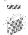
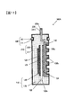
- FIG. 1 is an external perspective view of an electronic apparatus according to a first embodiment of the invention.
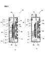
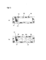
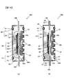
- 2A is a cross-sectional view taken along the line IIa-IIa in FIG. 1
- FIG. 2B is a cross-sectional view taken along the line IIb-IIb in FIG. 3A is a cross-sectional view of the electronic component structure
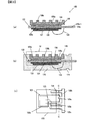
- FIG. 3B is a cross-sectional view for explaining the next step of FIG. 3A
- FIG. 3C is a lead before cutting.
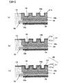
- 4A to 4C are cross-sectional views showing an example of a method for forming a conductor layer on an electronic module.
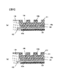
- FIG. 5A to 5B are cross-sectional views showing a second example of a method for forming a conductor layer on an electronic module.
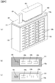
- FIG. 6A is a top view of the electronic module after electroless plating is performed, and FIG. 6B is an external perspective view for explaining a process following FIG. 6A.
- FIG. 7A is a top view of the electronic module for explaining a process following FIG. 6B, and FIG. 7B is a top view of the electronic module for explaining a process following FIG. 7A.
- FIG. 8A is an external perspective view of an electronic module for explaining a process before electroless plating, and FIG. 8B is an electronic module for explaining a process following FIG. 8A.
- FIG. 8C is a top view of the electronic module for explaining a process following FIG.
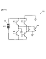
- FIG. 9A is a circuit diagram as an example of the circuit body of the present invention, and FIG. 9B is a timing chart of input / output signals of the circuit body.
- FIG. 10 is a circuit diagram of a circuit body of a comparative example.
- FIG. 11 is a cross-sectional view of Embodiment 2 of the electronic apparatus according to the invention.
- FIG. 12 is a cross-sectional view of Embodiment 3 of the electronic apparatus according to the invention.
- FIG. 13 is a cross-sectional view of Embodiment 4 of the electronic apparatus according to the invention.
- 14A is a cross-sectional view taken along line XIVa-XIVa of FIG. 13, and FIG.
- FIG. 14B is a cross-sectional view taken along line XIVb-XIVb of FIG.
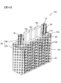
- FIG. 15 is an external perspective view of Embodiment 5 of the electronic apparatus according to the invention.
- FIG. 16 is an external perspective view of Embodiment 6 of an electronic apparatus according to the invention.
- FIG. 1 is an external perspective view of an electronic apparatus according to a first embodiment of the present invention
- FIG. 2 (a) is a cross-sectional view taken along the line IIa-IIa of FIG. 1
- FIG. 2 (b) is a cross-sectional view of FIG. It is IIb-IIb sectional view taken on the line.
- the electronic device 100 is mounted on, for example, a hybrid vehicle or an electric vehicle and used as a power conversion device that drives a motor or the like.
- the electronic device 100 includes an electronic module 110 and a conductor layer 200 provided in a region excluding a part on the upper surface side of the entire surface of the electronic module 110.
- the electronic module 110 includes an electronic component component 120 (see FIG. 3) and a sealing resin 170.
- the electronic component assembly 120 includes an electronic component 121, a bonding material 129, a lead frame (thermally conductive support member) 122 that is a metal member, a thermally conductive insulating member 124, and a heat sink 130. Yes.
- the electronic component component 120 has a plurality (three in the embodiment) of lead terminals 125a to 125c and a grounding terminal 126.
- the sealing resin 170 seals the entire periphery of the electronic component component 120 so that the leading ends of the lead terminals 125a to 125c and the ground terminal 126 and one surface of the heat sink 130 are exposed. In the vicinity of the upper surface side of the sealing resin 170, a groove 171 that goes around the peripheral side surface of the sealing resin 170 is formed.
- the conductor layer 200 includes a main body conductor layer 210 that covers one surface of the sealing resin 170 and the heat radiating plate 130, and a grounding conductor layer 220 that covers the grounding terminal 126.
- the main body conductor layer 210 and the grounding conductor layer 220 are electrically connected.
- Each of the lead terminals 125a to 125c is insulated from both the main body conductor layer 210 and the grounding conductor layer 220.
- the main body conductor layer 210 is also formed in the groove 171 of the sealing resin 170, and the seal member 181 is fitted in the groove 171 in a state of being in close contact with the outer surface of the main body conductor layer 210 formed in the groove 171. ing.
- the seal portion 180 is configured by the groove 171 of the sealing resin 170, the main body conductor layer 210 formed in the groove 171, and the seal member 181.
- the electronic device 100 is installed so as to be sealed by press-fitting a seal member 181 into the periphery of the opening of the flow path forming body in which a cooling path through which the cooling medium recirculates is formed. That is, the electronic device 100 is immersed in the cooling medium at a lower side than the seal portion 180.
- the electronic component 121 of the electronic component assembly 120 is formed of a semiconductor element that handles a large amount of power, such as an insulated gate transistor (IGBT).
- IGBT insulated gate transistor
- the power conversion device includes a plurality of semiconductor elements, but is illustrated as one electronic component 121 in FIGS.
- the back surface of the electronic component 121 is bonded to the die 122a of the lead frame 122 by a bonding material 129 such as solder.
- the lead frame 122 is made of copper, aluminum, or an alloy containing them as a main component.
- the lead terminals 125a to 125c are members that are formed integrally with the lead frame 122 by molding a sheet metal, and are separated by cutting the lead frame 122 after molding.
- an input electrode for inputting an input signal, an output electrode for outputting an output signal, and an input signal input from the input electrode are converted into an output signal.
- a control electrode for controlling the above is formed.
- Each electrode is bonded to the lead terminals 125a to 125c with a wire 123 formed of aluminum, gold or the like. That is, the lead terminals 125a to 125c have functions of an input terminal, a control terminal, and an output terminal, respectively.
- the electronic component 121 and the lead frame 122 are bonded by a wire 123 to constitute a circuit body 500 having an inverter circuit (see FIG. 9) described later.
- the ground terminal 126 is formed of a conductive member, and is insulated from all of the electronic component 121, the bonding material 129, the lead frame 122, and the heat sink 130. That is, the periphery of the grounding terminal 126 is covered with the sealing resin 170 in a state in which a part on the tip side is exposed.
- the grounding terminal 126 can be formed integrally with the lead frame 122 by molding a sheet metal, and can be formed by cutting and separating the lead frame 122 after molding. This will be described later.
- the thermally conductive insulating member 124 is interposed between the die 122a of the lead frame 122 and the heat radiating plate 130, and is formed of ceramics or organic resin.
- the heat sink 130 has a structure in which a plurality of cooling fins 130b arranged in a matrix or a staggered manner are integrally formed on a plate-shaped main body 130a.
- the heat radiating plate 130 is made of, for example, a metal containing aluminum, copper, magnesium, etc., ceramics having good thermal conductivity, a mixture of a metal and an inorganic material, or the like.
- machining by slice processing or dicer processing can be given.
- a heat sink 130 is formed.
- the vertical processing and the horizontal processing may be orthogonal to each other, or may be crossed obliquely. You may form by methods other than machining. You may use the clad material which makes the main body 130a and the cooling fin 130b a different material.
- the sealing resin 170 is formed of, for example, an epoxy resin or an organic resin material in which a filler such as silica is mixed with an epoxy resin. As described above, the sealing resin 170 exposes the leading ends of the lead terminals 125a to 125c and the grounding terminal 126 and one surface of the heat radiating plate 130 to seal almost the entire periphery of the electronic component component 120. Yes.
- the sealing resin 170 covers the entire periphery on the lower end side so that the grounding terminal 126 is insulated from other conductive members (see FIG. 2B).
- the outer surface of the sealing resin 170 on the side surface on which the heat radiating plate 130 is formed is substantially flush with the upper surface of the cooling fin 130b of the heat radiating plate 130 (see FIG. 3B).
- the main body conductor layer 210 includes a lower layer 211 and an upper layer 212 formed on the lower layer 211.
- a metal material such as aluminum, tin, chromium, copper, or nickel can be used.
- the lower layer 211 is preferably made of a copper-based metal having a low electrical resistivity.
- the material of the upper layer 212 is preferably a nickel-based metal that has high resistance in a use environment such as oxidation resistance.
- the grounding conductor layer 220 is formed of the same material as the lower layer 211 of the main body conductor layer 210. That is, the grounding conductor layer 220 includes only the lower layer 211 of the main body conductor layer 210 and does not include the upper layer 212 of the main body conductor layer 210.
- FIG. 3A is a cross-sectional view of the electronic component assembly 120
- FIG. 3B is a cross-sectional view for explaining the next step of FIG. 3A
- FIG. FIG. 4 is an example of a view of the lead frame before cutting viewed from the upper surface of FIG.
- the electronic component structure 120 is produced.
- a lead frame 122 in which the die 122a and the lead terminals 125a to 125c are integrated is formed.
- An electronic component 121 is bonded to one surface of the die 122a by a bonding material 129.
- As the bonding material 129 a soldering method using solder is preferable, but other methods may be used.
- the lead terminals 125 a to 125 c of the lead frame 122 are bonded to the electrodes (not shown) of the electronic component 121 and the wires 123 by wire bonding.
- the lead frame 122 is preferably cut to separate the lead terminals 125a to 125c and the die 122a. That is, as shown in FIG. 3C, the lead terminal 125a is connected to the die 122a, and the lead terminals 122b and 125c and the ground terminal 126 are separated from the die 122a to form a lead frame 122.
- the other ends of the lead terminals 125 a to 125 c and the ground terminal 126 are connected by the connecting portion 122 b of the lead frame 122.
- the electronic component 121 is bonded to the die 122a, the electrodes (not shown) of the electronic component 121 are bonded to the die 122a, and the lead terminals 125b and 125c and the electrodes of the electronic component 121 are wire-bonded (FIG. 3).
- the electronic component 121 and the wire 123 are indicated by dotted lines).
- the insulating member 124 and the heat radiating plate 130 are joined to the surface opposite to the surface where the electronic component 121 of the die 122a is joined.
- the insulating member 124 is formed of a resin, it is preferably a thermosetting resin having high heat conductivity.
- a resin having adhesiveness before being completely cured is interposed between the radiator plate 130 and the die 122a and thermocompression bonded to thermally cure the insulating member 124. This state is shown in FIG.
- a die 122a in which the electronic component 121 and the heat sink 130 are joined, lead terminals 125a to 125c connected to the electronic component 121 by wires 123, and a grounding terminal 126 are provided. Install in a mold (not shown).
- the sealing resin 170 is formed by molding.
- the transfer mold method is a preferable method.
- a groove 171 is formed in the sealing resin 170.
- the lead frame 122 is cut along a cutting line cc indicated by a two-dot chain line in FIG. 3C to separate the lead terminals 125a to 125c and the grounding terminal 126 from each other.
- the electronic module 110 is formed.
- the heat sink 130 is illustrated as having the cooling fins 130b as illustrated in FIG.
- the heat radiating plate 130 is a flat plate member on which the cooling fins 130b are not formed, the electronic component component 120 is sealed with a mold resin, the mold resin is cured, and the sealing resin 170 is removed. After the formation, the cooling fins 130b may be formed. According to this procedure, it is not necessary to take measures for preventing the mold resin from leaking from between the cooling fins 130b during the molding, so that the production can be made efficient. Next, a method for forming the conductor layer 200 on the electronic module 110 will be described.
- FIG. 4A the lower base layer 211a is formed by electroless plating. Since the heat dissipation plate 130 made of a metal member may corrode due to the liquidity of the electroless plating solution, the electroless plating solution needs to consider this point.
- the heat sink 130, the lead terminals 125a to 125c, and the grounding terminal 126 are formed of an aluminum-based metal
- the lower base layer 211 a may be formed on one surface of the heat sink 130 on the cooling fin 130 b side and on the ground terminal 126.
- the lower base layer 211 a may be formed on the sealing resin 170. In this embodiment, an example in which the lower base layer 211a is not formed on the sealing resin 170 is illustrated.
- the upper base layer 211b is formed on the lower base layer 211a and the sealing resin 170.
- the upper base layer 211b serves as a power feeding layer for electroplating (electrolytic plating) performed in the next step.
- the grounding conductor layer 220 is connected to a vehicle body or chassis (not shown) and serves as a surge current flow path.
- the upper base layer 211b is preferably made of a copper-based metal such as copper or a copper-nickel alloy having a low electrical resistivity.
- the upper base layer 211b is formed by electroless plating on the sealing resin 170 including the upper surface 170a, the entire surface on the cooling fin 130b side of the heat sink 130, and the grounding terminal 126 (FIG. 6B). reference).
- the lower base layer 211a and the upper base layer 211b constitute the lower layer 211.
- the upper layer 212 is formed on the upper base layer 211b.
- the upper layer 212 is formed by electroplating using the upper base layer 211b as a power feeding layer.
- the material of the upper layer 212 is preferably a nickel-based metal having high cost and high resistance such as oxidation resistance under the use environment.
- the upper layer 212 is not formed on the ground terminal 126, and the ground conductor layer 220 including only the lower layer 211 composed of the lower base layer 211 a and the upper base layer 211 b is formed on the ground terminal 126.
- the thickness of the lower layer 211 is about several hundred nm, and the thickness of the upper layer 212 is about several ⁇ m.
- the upper layer 212 can also be formed by electroless plating. Even when the upper layer 212 is formed by electroless plating, by forming the upper base layer 211b, it is possible to improve the depositing property of the plating metal during the electroless plating.
- An upper layer 212 is formed on the lower layer 211 constituted by the lower base layer 211a and the upper base layer 211b to form the main body conductor layer 210.
- FIG. 5A to 5B are cross-sectional views showing a second example of a method for forming a conductor layer on an electronic module.
- the lower layer 211 is formed by sputtering or vapor deposition.
- the lower layer 211 is formed on the sealing resin 170 and on the entire surface of the heat sink 130 on the cooling fin 130b side.
- the lower layer 211 is also formed on the ground terminal 126.
- a material of the lower layer 211 a copper-based metal is preferable.
- the thickness of the lower layer 211 is preferably 0.1 ⁇ m or more.
- titanium or chromium may be formed by sputtering or vapor deposition as a base metal before forming the copper-based metal.
- the thickness of the base metal may be about 30 to 130 nm.
- the upper layer 212 is formed on the lower layer 211.
- the upper layer 212 is formed by electroplating using the lower layer 211 as a power feeding layer.
- the upper layer 212 is not formed on the grounding terminal 126, and the grounding conductor layer 220 including only the lower layer 211 is formed on the grounding terminal 126.
- the main body conductor layer 210 is formed.
- a nickel-based metal can be used in consideration of resistance such as oxidation resistance in a use environment.
- the upper layer 212 can also be formed by electroless plating. Even when the upper layer 212 is formed by electroless plating, by forming the lower layer 211, it is possible to improve the depositing property of the plating metal during the electroless plating.
- the peripheral portions of the root portions of the lead terminals 125a to 125c of the sealing resin 170 are formed. It is necessary to prevent the conductor layer 200 from being formed.
- a method for preventing the conductor layer 200 from being formed on the periphery of the root portion where the lead terminals 125a to 125c of the sealing resin 170 are disposed will be described.
- FIG. 6A is a top view of the electronic module after the electroless plating is performed
- FIG. 6B is an external perspective view for explaining a process following FIG. 6A
- FIG. 7A is a top view of the electronic module for explaining the process following FIG. 6B
- FIG. 7B is for explaining the process following FIG. 7A. It is a top view of an electronic module.
- the lower layer 211 of the conductor layer 200 is formed on the entire surface of the electronic module 110. That is, the lower layer 211 is formed on the sealing resin 170, on one surface of the heat sink 130 on the cooling fin 130b side, and on the entire surface of the ground terminal 126 and the lead terminals 125a to 125c exposed from the sealing resin 170. .
- the lower layer 211 is formed by a method of forming the lower base layer 211a and the upper base layer 211b by electroless plating exemplified as the conductor layer forming method 1, or a lower layer by sputtering or vapor deposition exemplified as the conductor layer forming method 2. Any method of forming a 211 single layer may be used.
- the lead terminals 125 a to 125 c exposed from the sealing resin 170 are covered with a mask jig 401.
- An elastic sealing material 402 is provided at the lower end of the mask jig 401, and the sealing material 402 is pressure-bonded to the upper surface 170 a of the sealing resin 170 by the mask jig 401.
- the mask jig 401 has a size covering the entire lead terminals 125a to 125c, but three separate mask jigs covering the lead terminals 125a to 125c are used. May be.
- the upper layer 212 is formed by electroplating using the lower layer 211 as a power feeding layer.
- the electronic module 110 performs electroplating in a state where it is immersed in the plating solution so that the upper surface 170a of the sealing resin 170 is slightly submerged from the upper surface of the plating solution.
- the main body conductor layer 210 including the lower layer 211 and the upper layer 212 is formed on the entire sealing resin 170 including the one surface of the heat sink 130 on the cooling fin 130b side and the upper surface 170a.
- a grounding conductor layer 220 including only the lower layer 211 is formed on the grounding terminal 126.
- the electroplating is performed in a state where the sealing resin 170 is immersed in the plating solution so that the upper surface 170a of the sealing solution slightly sinks from the upper surface of the plating solution, the upper layer 212 is formed as shown in FIG.
- the grounding terminal 126 is plated to a height as thick as the thickness portion, and the amount of plating material can be reduced.
- the mask jig 401 is removed, and the lead terminals 125a to 125c are exposed. Then, the lower layer 211 formed on the exposed lead terminals 125a to 125c is removed. That is, the lower layer 211 formed on the lead terminals 125a to 125c is removed using the upper layer 212 as a mask. This state is illustrated in FIG.
- the lower layer 211 may be removed by dry etching or wet etching. Since the thickness of the upper layer 212 is thicker than the thickness of the lower layer 211, the lower layer 211 is etched using the upper layer 212 as a mask, and the etching may be terminated when the lower layer 211 is completely removed.
- the lower layer 211 formed on the upper surface 170a of the sealing resin 170 around the lead terminals 125a to 125c is removed together with the lower layer 211 formed on the lead terminals 125a to 125c by etching. As a result, the lead terminals 125a to 125c are insulated from the conductor layer 200, respectively.
- the lower layer 211 is formed on the entire upper surface 170a of the sealing resin 170, and the upper layer is formed on the lower layer 211 except for the peripheral edge portion of the base portion of the sealing resin 170 where the lead terminals 125a to 125c are arranged.
- the layer 212 is formed, and then the lower layer 211 at the roots of the lead terminals 125a to 125c is removed.
- FIG. 8A is an external perspective view of the electronic module for explaining the process before the electroless plating
- FIG. 8B is an electronic diagram for explaining the process following FIG. 8A
- FIG. 8C is a top view of the module
- FIG. 8C is a top view of the electronic module for explaining a process following FIG. 8B.
- a lower layer 211 is formed on the entire surface.
- the lower layer 211 is formed by forming the lower base layer 211a and the upper base layer 211b by electroless plating exemplified as the conductor layer forming method 1, and the lower layer by sputtering or vapor deposition exemplified as the conductor layer forming method 2. Any method of forming a 211 single layer may be used.
- the lower base layer 211a and the upper base layer 211b are formed by electroless plating, it is not necessary to immerse the entire electronic module 110 in the plating solution, so that the upper end portion side of the ground terminal 126 is exposed from the plating solution. Also good. That is, the lower base layer 211a and the upper base layer 211b may be formed up to an intermediate position between the root portion and the tip portion of the ground terminal 126.
- the upper layer 212 is formed by electroplating using the lower layer 211 as a power feeding layer.
- the electronic module 110 performs electroplating in a state where it is immersed in the plating solution so that the upper surface 170a of the sealing resin 170 is slightly submerged from the upper surface of the plating solution.
- the main body conductor layer 210 including the lower layer 211 and the upper layer 212 is formed on the entire sealing resin 170 including the one surface of the heat sink 130 on the cooling fin 130b side and the upper surface 170a.
- a grounding conductor layer 220 including only the lower layer 211 is formed on the grounding terminal 126. Thereafter, the mask jig 401 is removed.
- a method of covering the lead terminals 125a to 125c with the mask jig 401 provided with the sealing material 402 is illustrated.
- the periphery of the base portion of the sealing resin 170 on which the lead terminals 125a to 125c and the lead terminals 125a to 125c are arranged may be covered with clay or plaster.
- an O-ring is installed in the groove 171.
- the seal member 181 is press-fitted into the groove 171 of the sealing resin 170. Thereby, the electronic device 100 illustrated in FIG. 1 is formed.
- FIG. 9A is a circuit diagram as an example of the circuit body of the present invention
- FIG. 9B is a timing chart of input / output signals of the circuit body.
- the circuit body 500 includes, for example, an inverter circuit as illustrated.
- the circuit body 500 includes transistors 501 to 504 such as IGBTs and a DC power source 520, and an output terminal is connected to a load 519.
- the transistors 501 to 504 operate as switching elements. When the transistor 501 and the transistor 504 are simultaneously turned on, the output voltage Vo becomes E (v), which is the same as that of the DC power source 520 (see FIGS. 9B to 9).
- the output voltage Vo becomes ⁇ E (v) (see FIGS. 9B to 9B).
- the transistors 501 to 504 are all off, the output voltage Vo is 0 (v).
- the drive waveforms shown in FIGS. 9B to 9C are output. Furthermore, by performing fine control, it is possible to approximate the AC waveform.
- Each of the transistors 501 to 504 is usually mounted with the collector electrode facing the die 122a side of the lead frame 122 and the gate electrode and emitter electrode facing the opposite side.
- the collector electrode is electrically connected to the die 122a of the lead frame 122 through the bonding material 129.
- the grounding terminal 126 is connected to a vehicle body or chassis having a ground potential.
- the grounding terminal 126 is electrically connected to the heat sink 130 via the grounding conductor layer 220 and the main body conductor layer 210. Since the insulating member 124 is interposed between the die 122a of the lead frame 122 and the heat sink 130, the collector electrodes of the transistors 501 to 504 are insulated from the grounded portion, as shown in FIGS. 9B to 9C.
- the illustrated output signal is supplied to the load 519.
- FIG. 10 is a circuit diagram of the circuit body 500A of the comparative example.
- the circuit body 500A of the comparative example is a case where the insulating member 124 is not interposed between the die 122a of the lead frame 122 and the heat sink 130. Even in this case, the grounding terminal 126 is electrically connected to the heat sink 130 via the grounding conductor layer 220 and the main body conductor layer 210, and the grounding terminal 126 is connected to the vehicle body, chassis or the like to be grounded.
- the structure is as follows.
- the collector electrodes of the transistors 501 to 504 are connected via the die 122a of the lead frame 122, the heat sink 130, the main body conductor layer 210, the ground conductor layer 220, and the ground terminal 126. Grounded. For this reason, the output voltage Vo becomes the same potential as the ground potential both when the transistor 501 and the transistor 504 are turned on simultaneously and when the transistor 502 and the transistor 503 are turned on simultaneously. That is, an AC waveform cannot be obtained. Therefore, the transistors 501 to 504 of the circuit body 500 need to be insulated from the main body conductor layer 210 and the grounding conductor layer 220.
- the electronic device has the following effects.
- the power supply line of the circuit body 500 is insulated from the heat sink 130, the grounding terminal 126 is provided in the electronic component component 120, and the grounding terminal 126 is electrically connected to the conductor layer 200. For this reason, by grounding the grounding terminal 126, a surge voltage generated when the circuit body 500 performs a switching operation can be suppressed.
- the conductor layer 200 is constituted by a main body conductor layer 210 formed on one surface of the heat radiating plate 130 and the sealing resin 170 and a ground conductor layer 220 formed on the ground terminal 126.
- the grounding conductor layer 220 is composed of the lower layer 211 having a low electrical resistivity, and does not have the upper layer 212 having a high electrical resistivity. For this reason, when the grounding conductor layer 220 is grounded, the resistance value of the connection portion becomes small, and the surge voltage reduction efficiency is good.
- the main body conductor layer 210 has an upper layer 212 made of a nickel-based metal or the like that is formed on the lower layer 211 having a low electric resistivity, for example, having high resistance such as oxidation resistance under the use environment. For this reason, the production cost of a plating layer can be reduced and it can be made reliable with respect to a use environment.
- a lower base layer 211a made of electroless nickel plating is formed on the lower layer 211 of the conductor layer 200, and an upper base layer 211b made of a copper-based metal having a low electrical resistivity is electrolessly formed on the lower base layer 211a. It was formed by plating. Therefore, even when the heat sink 130, the conductive leads (lead terminals) 125a to 125c or the grounding terminal 126 are formed of an aluminum-based metal, they are corroded by the copper-based metal electroless plating solution. Can be suppressed.
- the lower layer 211 made of a copper-based metal is formed on the heat sink 130 by sputtering or vapor deposition.
- the lower layer 211 can be formed directly without using another metal material. Therefore, production efficiency can be improved.
- the bonding reliability can be improved by interposing a base metal such as titanium or chromium. it can.
- the lower layer 211 of the conductor layer 200 is formed on the entire electronic module 110, and the periphery of the base portion of the sealing resin 170 on which the lead terminals 125a to 125c and the lead terminals 125a to 125c are arranged is masked with a mask jig 401. Then, the upper layer 212 was formed, and thereafter, the lower layer 211 at the periphery of the base portion of the sealing resin 170 on which the lead terminals 125a to 125c were arranged was removed using the upper layer 212 as a mask. Since the lower layer 211 at the periphery of the base portion of the sealing resin 170 on which the lead terminals 125a to 125c are arranged is removed using the upper layer 212 as a mask, the working efficiency is good.
- the lead terminals 125a to 125c are covered with the mask jig 401, and then the lower layer 211 and the upper layer 212 of the conductor layer 200 are formed.
- the process of removing the lower layer 211 of the conductor layer 200 is not necessary, and the number of processes is reduced, so that the working efficiency can be further improved.
- FIG. 11 is a cross-sectional view of Embodiment 2 of the electronic apparatus according to the invention.
- the electronic device 100A of the second embodiment is different from the electronic device 100 of the first embodiment in that the grounding terminal 126a is electrically connected to the heat sink 130.
- the configuration in which the grounding terminal 126a is linearly arranged on the upper surface 170a of the sealing resin 170 together with the lead terminals 125a to 125c is the same as that of the electronic device 100 of the first embodiment.
- the grounding terminal 126a of the second embodiment is bent toward the heat radiating plate 130, and its end is electrically connected to the heat radiating plate 130 by soldering, welding, or the like. Yes.
- FIG. 12 is a cross-sectional view of Embodiment 3 of the electronic apparatus according to the invention.
- the electronic device 100B of the third embodiment will be described mainly with respect to differences from the electronic device 100 of the first embodiment.
- the electronic device 100 ⁇ / b> B of the third embodiment includes a counter heat dissipation structure 610 on the opposite side of the heat dissipation plate 130 in the electronic component 121.
- the counter heat dissipation structure 610 includes an intermediate heat transfer body 611, a counter insulating member 612, and a counter heat sink 613.
- the intermediate heat transfer body 611 is formed of a high heat transfer metal such as copper or aluminum metal or a ceramic such as alumina.
- the opposing insulating member 612 is a member similar to the insulating member 124, and is formed of ceramics or organic resin.
- the counter heat sink 613 is a member similar to the heat sink 130 and includes a main body 613a and cooling fins 613b.
- the intermediate heat transfer body 611 is interposed between the electronic component 121 and the opposing insulating member 612, and one surface thereof is thermally coupled to one surface of the electronic component 121, and the other surface is thermally coupled to one surface of the opposing insulating member 612. ing.
- the electronic component 121 includes a transistor such as an IGBT, and an emitter electrode (not shown) of the transistor is thermally coupled to the intermediate heat transfer body 611. As described above, the cathode electrode of the transistor is thermally coupled to the die 122a of the lead frame 122 through the bonding material 129.
- the electronic component structure 120A of the third embodiment has a structure in which the counter heat dissipation structure 610 is thermally coupled to the electronic component 121 of the electronic component structure 120 of the first embodiment.
- the sealing resin 170A seals the electronic component constituting body 120A so that one surface of the heat radiating plate 130, one surface of the counter heat radiating plate 613, the lead terminals 125a to 125c, and the tip ends of the grounding terminals 126 are exposed. Since the other configuration of the electronic device 100B according to the third embodiment is the same as that of the electronic device 100 according to the first embodiment, the corresponding members are denoted by the same reference numerals and description thereof is omitted.
- the electronic device 100B of the third embodiment also has the same effect as the electronic device 100 of the first embodiment. Moreover, in the electronic device 100B of Embodiment 3, since the heat sinks 130 and 613 are provided on both surfaces of the electronic component 121, the heat dissipation effect of the electronic component 121 can be enhanced.
- FIG. 13 is a cross-sectional view of Embodiment 4 of the electronic apparatus of the present invention.
- 14A is a cross-sectional view taken along line XIVa-XIVa in FIG. 13, and FIG. 14B is a cross-sectional view taken along line XIVb-XIVb in FIG.
- a seal portion 180A similar to the seal portion 180 provided on the upper side is also provided on the lower side.
- 180 A of sealing parts are comprised by the groove
- the upper and lower end portions are arranged outside the cooling flow path through which the refrigerant flows, in other words, the central region between the seal portion 180 and the seal portion 180A is cooled. It is installed in a flow path forming body (not shown) so as to be immersed in the medium.
- lead terminals 125d to 125f are formed to protrude from the sealing resin 170 on the lower surface side of the electronic module 110.
- the lead terminals 125d to 125f are connected to the die 122a of the lead frame 122 by wires 123, respectively.
- the lead terminals 125d to 125f are insulated from the conductor layer 200, like the lead terminals 125a to 125c.
- the grounding terminal 126 b is formed to protrude from the sealing resin 170 on the lower surface side of the electronic module 110.
- the grounding terminal 126b is insulated from the lead frame 122, the electronic component 121, the bonding material 129, and the like.
- the ground terminals 126 and 126 b are illustrated as being insulated from the heat sink 130, but as in the second embodiment illustrated in FIG. 11, the ground terminals 126 and 126 b Both or one may be electrically connected to the heat sink 130.
- the grounding conductor layer 220 is formed on the grounding terminal 126b.
- the grounding conductor layer 220 is made of the same material as the lower layer 211 of the main body conductor layer 210 and is electrically connected to the main body conductor layer 210.
- the other structure in Embodiment 4 is the same as that of Embodiment 1, attaches
- FIG. 15 is an external perspective view of Embodiment 5 of the electronic apparatus according to the invention.
- the base portion 141 of the grounding terminal 126 has the same configuration as that of the main body conductor layer 210.
- the main body conductor layer 210 has the lower layer 211 and the upper layer 212.
- the lower layer 211 is formed on the entire outer surface of the electronic module 110 including the outer surface of the ground terminal 126, and the upper layer 212 is formed on the lower layer 211.
- the electronic module 110 when the upper layer 212 is formed, the electronic module 110 is electroplated in a state where the electronic module 110 is immersed in the plating solution so that the upper surface 170a of the sealing resin 170 slightly sinks from the upper surface of the plating solution. .
- the plating material can be saved. However, it may be considered that the connection between the lower layer 211 and the upper layer 212 at the base of the ground terminal 126 becomes unstable.
- the fifth embodiment when the upper layer 212 is formed, electroplating is performed in a state where the electronic module 110 is immersed in the plating solution up to the root portion 141 of the ground terminal 126. Thereby, the base portion 141 of the grounding terminal 126 is formed in the same plating layer structure as that of the main body conductor layer 210.
- Other structures in the fifth embodiment are the same as those in the first embodiment, and the corresponding members are denoted by the same reference numerals and description thereof is omitted. Therefore, the fifth embodiment has the same configuration as that of the first embodiment.
- the electrical connection between the lower layer 211 and the upper layer 212 of the ground terminal 126 can be made more reliable. Note that the structure of the electronic device 100D of the fifth embodiment can also be applied to the electronic devices 100A to 100C of the second to fourth embodiments.
- FIG. 16 is an external perspective view of Embodiment 6 of the electronic apparatus according to the invention.
- the electronic device 100E according to the sixth embodiment illustrated in FIG. 16 includes a plurality (two in FIG. 16) of ground terminals 126 and 142.
- a grounding conductor layer 220 is formed on each of the grounding terminals 126 and 142.
- the grounding terminals 126 and 142 are provided so as to face the ends in the longitudinal direction of the upper surface 170 a of the sealing resin 170.
- the grounding conductor layer 220 is formed integrally with the lower layer 211 of the main body conductor layer 210 and does not have the upper layer 212 of the main body conductor layer 210.
- the ground terminal 126 is exemplified as a structure provided on the upper surface 170a of the sealing resin 170.
- the grounding terminal 126 may be provided on the other side surface of the sealing resin 170.
- it is preferably provided outside the seal part 180.
- the electronic component 121 is exemplified as a structure mounted on the lead frame 122.
- the member on which the electronic component 121 is mounted is not limited to the lead frame 122, and may be another supporting member having thermal conductivity such as metal or ceramic.
- the grounding conductor layer 220 is illustrated as being formed on the entire surface of the grounding terminals 126, 126a, 126b, and 142. However, the grounding conductor layer 220 may be formed only on a part of the base side of the grounding terminals 126, 126 a, 126 b and 142.
- the electronic module 110 is protruded from the plating layer. It was exemplified by a method of electroplating by immersing in a plating layer.
- the grounding terminal 126 may be electroplated by being immersed in a plating solution in a state of being covered with a mask jig in the same manner as the lead terminals 125a to 125c.
- the ground layer terminals 126, 126a, 126b, 142 are exemplified as a structure in which the upper layer 212 is not formed on at least a part thereof. However, the entire surface of the grounding terminals 126, 126 a, 126 b, 142 may be covered with the upper layer 212.
- the heat radiating plate 130 is exemplified as a structure having the cooling fins 130b.
- the heat sink 130 may not have the cooling fins 130b.
- the insulating member 124 is exemplified as a structure directly joined to the heat sink 130.
- an intermediate heat transfer plate (not shown) may be joined to the heat radiating plate 130 and the insulating member 124 may be joined to the intermediate heat transfer plate.
- the heat sink 130 is embedded in the sealing resin 170 so that the upper surface of the cooling fin 130b of the heat sink 130 is substantially flush with the outer surface of the sealing resin 170.
- the main body 130a of the heat radiating plate 130 may be embedded in the sealing resin 170 to the middle of its thickness.
- the heat dissipation plate 130 may be structured not to be embedded in the sealing resin 170. In this case, the bonding strength between the heat sink 130 and the insulating member 124 is increased, or an intermediate metal plate (not shown) is metal bonded to the heat sink 130 and the intermediate metal plate is embedded in the sealing resin 170. It is preferable to have a structure.
- the circuit body 500 has an inverter circuit, but the present invention can also be applied when the circuit body 500 has another power conversion circuit such as a converter circuit.
- the present invention can be arbitrarily modified and applied within the scope of the gist of the present invention.
- a part of each of the input terminal, the output terminal and the ground terminal, and one surface of the heat sink An electronic device that is exposed and whose periphery is covered with a sealing resin, the input terminal and the output terminal being insulated from each other, and a cooling medium between the sealing resin and one surface of the heat sink
Landscapes
- Cooling Or The Like Of Semiconductors Or Solid State Devices (AREA)
- Structures Or Materials For Encapsulating Or Coating Semiconductor Devices Or Solid State Devices (AREA)
- Engineering & Computer Science (AREA)
- Manufacturing & Machinery (AREA)
Abstract
Description
以下、図1~図10を参照して、本発明に係る電子機器およびその製造方法の一実施の形態を説明する。
[電子機器の構造]
図1は、本発明の電子機器の実施形態1としての外観斜視図であり、図2(a)は、図1のIIa-IIa線断面図であり、図2(b)は、図1のIIb-IIb線断面図である。
電子機器100は、例えば、ハイブリッド自動車や電気自動車に搭載され、モータ等を駆動する電力変換装置として用いられる。
電子機器100は、電子モジュール110と、電子モジュール110の全表面のうち、上面側の一部を除く領域に設けられた導体層200とを備えている。電子モジュール110は、電子部品構成体120(図3参照)と、封止樹脂170とを備えている。
封止樹脂170は、リード端子125a~125cおよび接地用端子126の先端側、および放熱板130の一面が露出されるように、電子部品構成体120の周囲全体を封止している。
封止樹脂170の上面側近傍には、封止樹脂170の周側面を1周りする溝171が形成されている。
本体導体層210は、封止樹脂170の溝171内にも形成されており、溝171内に形成された本体導体層210の外面に密着した状態で、溝171内にシール部材181が嵌入されている。つまり、封止樹脂170の溝171と、溝171内に形成された本体導体層210と、シール部材181とによりシール部180が構成されている。電子機器100は、図示はしないが、冷却媒体が還流する冷却路が形成された流路形成体の開口部周縁にシール部材181を圧入して密封するように設置される。つまり、電子機器100は、シール部180より下側が、冷却媒体中に浸漬される。
電子部品121は、その裏面がはんだ等の接合材129により、リードフレーム122のダイ122aに接合されている。リードフレーム122は、銅、アルミニウムまたはそれらを主成分とする合金により形成されている。リード端子125a~125cは、板金の成形加工によりリードフレーム122と一体に形成し、成形後にリードフレーム122を切断して分離された部材である。
接地用端子126は、リード端子125a~125cと同様、板金の成形加工によりリードフレーム122と一体に形成し、成形後にリードフレーム122を切断して分離することにより形成することもできる。このことについては、後述する。
上述した通り、封止樹脂170は、リード端子125a~125cおよび接地用端子126の先端側、および放熱板130の一面を露出して、電子部品構成体120の周囲のほぼ全体を封止している。封止樹脂170は、接地用端子126を他の導電性の部材から絶縁されるように、その下端部側の周囲全体を覆っている(図2(b)参照)。封止樹脂170は、放熱板130が形成された側面では、その外表面が、放熱板130の冷却フィン130bの上面と、ほぼ面一となっている(図3(b)参照)。
接地用導体層220は、本体導体層210の下部層211と同一の材料により形成されている。つまり、接地用導体層220は、本体導体層210の下部層211のみを有し、本体導体層210の上部層212を有していない。
電子モジュール110の製造方法の一実施の形態を説明する。
図3(a)は、電子部品構成体120の断面図であり、図3(b)は、図3(a)の次の工程を説明するための断面図であり、図3(c)は、切断前のリードフレームを図3(b)の上面から観た図の一例である。
先ず、電子部品構成体120を作製する。
ダイ122aおよびリード端子125a~125cが一体化されたリードフレーム122を形成する。ダイ122aの一面に電子部品121を接合材129により接合する。接合材129として、はんだを用い、はんだ付けする方法が好ましいが、他の方法でもよい。次に、ワイヤボンディングにより、リードフレーム122のリード端子125a~125cそれぞれを電子部品121の電極(図示せず)とワイヤ123によりボンディングする。リード端子125a~125cと電子部品121の電極とをワイヤボンディングする前に、リードフレーム122を切断してリード端子125a~125cとダイ122aを分離しておくことが好ましい。
すなわち、図3(c)に図示されるように、リード端子125aがダイ122aに接続され、リード端子125b、125cおよび接地用端子126がダイ122aから分離されたリードフレーム122を形成する。この時点では、リード端子125a~125c、および接地用端子126の他端は、リードフレーム122の連結部122bにより連結されている。この後、電子部品121をダイ122aに接合して、ダイ122aに電子部品121の電極(不図示)をボンディングすると共に、リード端子125b、125cと電子部品121の電極とをワイヤボンディングする(図3(c)では、電子部品121およびワイヤ123を点線で示す)。
このようにして、電子モジュール110が形成される。
なお、上記において、電子部品構成体120を形成する際、図3(a)に図示されるように、放熱板130には、冷却フィン130bが形成されているものとして例示されている。しかし、この段階では、放熱板130は、冷却フィン130bが形成されていない平板状の部材としておき、電子部品構成体120をモールド樹脂により封止し、モールド樹脂を硬化して封止樹脂170を形成した後、冷却フィン130bを形成するようにしてもよい。この手順にすると、モールド成形の際、冷却フィン130b間からモールド樹脂が漏出するのを防止するための手段を講じる必要がないので、生産を効率的にすることができる。
次に、電子モジュール110に導体層200を形成する方法を説明する。
図4(a)~4(c)は、電子モジュールに導体層を形成する方法の一例を示す断面図である。導体層の形成方法は、図3(b)の領域IVを拡大した図で説明する。
封止樹脂170上に本体導体層210の上部層212を電気めっきで形成するには、給電膜となる下部層211が必要となる。
そこで、先ず、図4(a)に図示されるように、下層下地層211aを、無電解めっきにより形成する。無電解めっき液の液性により、金属製部材からなる放熱板130が腐食することがあるので、無電解めっき液は、この点を配慮する必要がある。このため、例えば、放熱板130、リード端子125a~125c、および接地用端子126がアルミニウム系金属により形成されている場合、下層下地層211aの形成には無電解ニッケルめっきを用いることが好ましい。
下層下地層211aは、放熱板130の冷却フィン130b側の一面上および接地用端子126上に形成すればよい。しかし、下層下地層211aを、封止樹脂170上に形成してもよい。この実施の形態では、封止樹脂170上には、下層下地層211aを形成しない例で図示されている。
上部層212は、接地用端子126には形成せず、接地用端子126上には、下層下地層211aおよび上層下地層211bにより構成される下部層211のみからなる接地用導体層220が形成される。下部層211の厚さは、数百nm程度、上部層212の厚さは数μm程度とする。
下層下地層211aおよび上層下地層211bにより構成される下部層211上に、上部層212が形成されて本体導体層210が構成される。
図5(a)~5(b)は、電子モジュールに導体層を形成する方法の第2の例を示す断面図である。
導体層200を形成する第2の方法は、先ず、図5(a)に図示されるように、下部層211を、スパッタまたは蒸着により形成する。下部層211は、封止樹脂170上、放熱板130の冷却フィン130b側の一面上全体に形成する。また、下部層211は、接地用端子126上にも形成される。下部層211の材料として、銅系金属が好ましい。下部層211の厚さは、0.1μm以上であることが好ましい。封止樹脂170および放熱板130と銅系金属との接着力が不足する場合、銅系金属形成前に、下地金属として、チタン、クロムをスパッタまたは蒸着により形成してもよい。下地金属の厚さは、30~130nm程度あればよい。
上部層212は、無電解めっきにより形成することも可能である。上部層212を無電解めっきにより形成する場合でも、下部層211を形成しておくことにより、無電解めっき時のめっき金属の析出性を向上することができる。
次に、封止樹脂170のリード端子125a~125cが配置された根元部の周縁部に、導体層200が形成されないようにする方法について説明する。
図6(a)、(b)~図7(a)、(b)を参照して、リード端子125a~125cへの導体層200の付着を防止する方法を説明する。
図6(a)は、無電解めっきを行った後の電子モジュールの上面図であり、図6(b)は、図6(a)に続く工程を説明するための外観斜視図である。また、図7(a)は、図6(b)に続く工程を説明するための電子モジュールの上面図であり、図7(b)は、図7(a)に続く工程を説明するための電子モジュールの上面図である。
先ず、図6(a)に図示されるように、導体層200の下部層211を、電子モジュール110の全表面に形成する。すなわち、封止樹脂170上、放熱板130の冷却フィン130b側の一面上、および封止樹脂170から露出した部分の接地用端子126およびリード端子125a~125cの全表面に下部層211を形成する。
下部層211の形成は、導体層の形成方法1として例示した無電解めっきによる下層下地層211aおよび上層下地層211bを形成する方法、または導体層の形成方法2として例示したスパッタまたは蒸着による下部層211単層を形成する方法のいずれでもよい。
これに対して、下部層211および上部層212を、封止樹脂170のリード端子125a~125cが配置された根元部の周縁部に形成しない方法を用いることもできる。以下に、その方法を説明する。
図8(a)は、無電解めっきを行う前の工程を説明するための電子モジュールの外観斜視図であり、図8(b)は、図8(a)に続く工程を説明するための電子モジュールの上面図であり、図8(c)は、図8(b)に続く工程を説明するための電子モジュールの上面図である。
最初に、図8(a)に図示するように、封止樹脂170から露出したリード端子125a~125cをマスク治具401で覆う。マスク治具401の下端には弾性を有するシール材402が設けられており、マスク治具401によりシール材402を封止樹脂170の上面170aに圧着する。
無電解めっきにより下層下地層211aおよび上層下地層211bを形成する場合、電子モジュール110全体をめっき液中に浸漬する必要はなく、接地用端子126の上部先端部側がめっき液から露出するようにしてもよい。つまり、下層下地層211aおよび上層下地層211bは、接地用端子126の根元部と先端部との中間位置まで形成するようにしてもよい。
この後、マスク治具401を取り外す。
図9(a)は、本発明の回路体が有する一例としての回路図であり、図9(b)は、回路体の入出力信号のタイミングチャートである。
回路体500は、例えば、図示のようなインバータ回路を有する。回路体500は、IGBT等のトランジスタ501~504、直流電源520を有し、出力端が負荷519に接続される。トランジスタ501~504は、スイッチング素子として動作する。トランジスタ501とトランジスタ504が同時にオンすると、出力電圧Voは、直流電源520と同じE(v)になる(図9(b)-(1)参照)。トランジスタ502とトランジスタ503が同時にオンすると、出力電圧Voは、-E(v)になる(図9(b)-(2)参照)。トランジスタ501~504がすべてオフ状態では、出力電圧Voは0(v)になる。
トランジスタ501~504のオン・オフ動作を制御することで、図9(b)-(3)に図示される駆動波形が出力される。さらに、細かな制御を行うことで、交流波形に近づけることができる。
接地用端子126は、接地電位を有する車両のボディやシャーシ等に接続される。接地用端子126は、接地用導体層220および本体導体層210を介して放熱板130に電気的に接続されている。リードフレーム122のダイ122aと放熱板130との間に絶縁部材124が介在されることで、各トランジスタ501~504のコレクタ電極は、接地部位から絶縁され、図9(b)-(3)に図示される出力信号を負荷519に供給する。
比較例の回路体500Aは、リードフレーム122のダイ122aと放熱板130との間に絶縁部材124が介在されていない場合である。この場合でも、接地用端子126は、接地用導体層220および本体導体層210を介して放熱板130に電気的に接続され、接地用端子126が、車両のボディやシャーシ等に接続して接地された構造とする。このような回路体500Aでは、図示のように、トランジスタ501~504のコレクタ電極は、リードフレーム122のダイ122a、放熱板130、本体導体層210、接地用導体層220および接地用端子126を介して接地される。このため、トランジスタ501とトランジスタ504が同時にオンした場合も、トランジスタ502とトランジスタ503が同時にオンした場合も、出力電圧Voは、接地電位と同電位になる。つまり、交流波形は得られない。
このことから、回路体500のトランジスタ501~504は、本体導体層210および接地用導体層220から絶縁する必要がある。
(1)回路体500および放熱板130を備える電子部品構成体120を封止樹脂170により封止し、放熱板130の一面および封止樹脂170に導体層200を設けた。また、回路体500の給電ラインを放熱板130とは絶縁するとともに、電子部品構成体120に接地用端子126を設け、接地用端子126を導体層200に電気的に接続した。このため、接地用端子126を接地することにより、回路体500がスイッチング動作するときに発生するサージ電圧を抑制することができる。
図11は、本発明の電子機器の実施形態2の断面図である。
実施形態2の電子機器100Aは、接地用端子126aが、放熱板130に電気的に接続されている点で、実施形態1の電子機器100と相違する。
接地用端子126aは、リード端子125a~125cと共に、封止樹脂170の上面170a上で、直線状に配置されている構成は、実施形態1の電子機器100と同様である。
実施形態2の接地用端子126aは、封止樹脂170に埋設された部分において、放熱板130側に屈曲され、その端部が放熱板130に、半田付や溶接等により電気的に接続されている。
実施形態2の電子機器100Aの他の構成は、実施形態1の電子機器100と同様であり、対応する部材に同一の符号を付して説明を省略する。
実施形態2においても、実施形態1と同様な効果を奏する。
実施形態2では、接地用端子126aが放熱板130にも電気的に接続されているので、サージ電圧の抑制が一層確実となる。
図12は、本発明の電子機器の実施形態3の断面図である。
実施形態3の電子機器100Bについて、実施形態1の電子機器100との相違点を主体として説明する。
実施形態3の電子機器100Bは、電子部品121における放熱板130の反対側に、対向放熱構造部610を備えている。対向放熱構造部610は、中間伝熱体611と、対向絶縁部材612と、対向放熱板613とを備えている。
実施形態3の電子機器100Bの他の構成は実施形態1の電子機器100と同様であるので、対応する部材に同一の符号を付して説明を省略する。
図13は、本発明の電子機器の実施形態4の断面図である。図14(a)は、図13のXIVa-XIVa線断面図であり、図14(b)は、図13のXIVb-XIVb線断面図である。
実施形態4の電子機器100Cは、上部側に設けられたシール部180と同様なシール部180Aが下部側にも設けられている。シール部180Aは、封止樹脂170に形成された溝171と、溝171内に形成された本体導体層210と、シール部材181とにより構成されている。実施形態4の電子機器100Cは、その上下の端部が、冷媒が流れる冷却流路の外側に配置された状態に、換言すれば、シール部180とシール部180Aとの間の中央領域が冷却媒体に浸漬するように、不図示の流路形成体に設置される。
また、電子モジュール110の上面側に封止樹脂170から突出して形成された接地用端子126と同様、電子モジュール110の下面側に接地用端子126bが封止樹脂170から突出して形成されている。接地用端子126bは、接地用端子126と同様、リードフレーム122、電子部品121、接合材129等とは絶縁されている。なお、図13において、接地用端子126、126bは、放熱板130とは絶縁された状態に図示されているが、図11に図示された実施形態2のように、接地用端子126、126bの双方または一方を、放熱板130に電気的に接続してもよい。
なお、実施形態4における他の構造は、実施形態1と同様であり、対応する部材に同一の符号を付して、説明を省略する。
従って、実施形態4においても、実施形態1と同様な効果を奏する。
図15は、本発明の電子機器の実施形態5の外観斜視図である。
図15に図示された実施形態5の電子機器100Dは、接地用端子126の根元部141を本体導体層210と同一の構成としたものである。上述した通り、本体導体層210は、下部層211と上部層212とを有する。
下部層211は、接地用端子126の外表面を含む電子モジュール110の外表面全体に形成し、下部層211上に上部層212を形成する。実施形態1では、上部層212を形成するとき、電子モジュール110を、封止樹脂170の上面170aがめっき液の上面より僅かに沈むようにめっき液中に浸漬した状態で電気めっきを行うこととした。この方法では、接地用端子126の根元部には、上部層212は形成されないので、めっき材料の節減ができる。しかし、接地用端子126の根元部における下部層211と上部層212との接続が、不安定になることも考えられる。
実施形態5における他の構造は、実施形態1と同様であり、対応する部材に同一の符号を付して説明を省略する。
従って、実施形態5においても、実施形態1と同様な構成を有する。実施形態5では、特に、接地用端子126の下部層211と上部層212との電気的接続をより確実にすることができる。
なお、実施形態2~4の電子機器100A~100Cにおいても、実施形態5の電子機器100Dの構造を適用することができる。
図16は、本発明の電子機器の実施形態6の外観斜視図である。
図16に図示された実施形態6の電子機器100Eは、複数(図16では2つ)の接地用端子126、142を有する。
接地用端子126、142それぞれには、接地用導体層220が形成されている。接地用端子126および142は、封止樹脂170の上面170aの長手方向の端部に対向して設けられている。上述した各実施形態と同様、接地用導体層220は、本体導体層210の下部層211と一体に形成され、本体導体層210の上部層212を有していない。
実施形態6の電子機器100Eの他の構造は、実施形態1と同様であり、対応する部材に同一の符号を付して説明を省略する。
実施形態6においても、実施形態1と同様な効果を奏する。実施形態6では、特に、複数の接地用端子126、142を有しているので、サージ電圧の抑制をより確実に行うことができる。
実施形態2~5においても、実施形態6の構造を適用することができる。
日本国特許出願2014年第220440号(2014年10月29日出願)
110 電子モジュール
120、120A 電子部品構成体
121 電子部品
122 リードフレーム(熱伝導性支持部材)
123 ワイヤ
124 絶縁部材
125a~125f リード端子(入力用端子、制御用端子、出力用端子)
126、126a、126b、142 接地用端子
129 接合材
130 放熱板
130a 本体
130b 冷却フィン
141 根元部
170、170A 封止樹脂
171 溝
180、180A シール部
181 シール部材
200 導体層
210 本体導体層
211 下部層
211a 下層下地層
211b 上層下地層
212 上部層
220 接地用導体層
401 マスク治具
402 シール材
500 回路体
501~504 トランジスタ(半導体素子)
610 対向放熱構造部
611 中間伝熱体
612 対向絶縁部材
613 対向放熱板
613a 本体
613b 冷却フィン
Claims (15)
- 入力用電極と出力用電極とを有する半導体素子、および前記半導体素子を支持する熱伝導性支持部材を有する回路体と、前記回路体の一面に熱伝導可能に設けられた放熱板と、前記放熱板と前記熱伝導性支持部材との間に介装された熱伝導性の絶縁部材と、前記入力用電極に接続された入力用端子と、前記出力用電極に接続された出力用端子と、接地用端子とを備えた電子部品構成体と、
前記入力用端子、前記出力用端子および前記接地用端子それぞれの一部、および前記放熱板の一面を露出して、前記電子部品構成体の周囲を覆って形成された封止樹脂と、
前記入力用端子および前記出力用端子とは絶縁されて形成され、前記封止樹脂と前記放熱板の一面との冷却媒体への浸漬領域の全面を覆って形成された本体導体層と、
前記接地用端子の少なくとも一部を覆い、前記本体導体層と電気的に接続されている接地用導体層と、を備える、電子機器。 - 請求項1に記載の電子機器において、
前記半導体素子は、制御信号が入力される制御用電極を有し、
前記回路体は、電力変換回路を構成する複数の前記半導体素子と、前記制御用電極に接続され、前記本体導体層および前記接地用導体層とは絶縁された制御用端子とを有する、電子機器。 - 請求項1に記載の電子機器において、
前記放熱板は、複数の冷却用フィンを有し、前記本体導体層は、前記冷却用フィンそれぞれの表面を覆って形成されている、電子機器。 - 請求項1に記載の電子機器において、
前記熱伝導性支持部材は、金属製のリードフレームであり、前記入力用端子、前記出力用端子および前記接地用端子は、前記リードフレームから分離されて形成されたリードである、電子機器。 - 請求項1に記載の電子機器において、
前記接地用端子は、前記熱伝導性支持部材に電気的に接続されている、電子機器。 - 請求項1に記載の電子機器において、
前記接地用端子を複数個有し、前記接地用端子のそれぞれの少なくとも一部には、前記本体導体層と電気的に接続された前記接地用導体層が形成されている、電子機器。 - 請求項1に記載の電子機器において、
前記電子部品構成体の周囲を覆って形成された前記封止樹脂は、前記放熱板が配置された一面と、前記一面に隣接し、前記入力用端子、前記出力用端子および前記接地用端子が配置された側面とを有し、前記一面における前記側面との境界部の近傍にシール部を備える、電子機器。 - 請求項7に記載の電子機器において、
前記シール部は、前記封止樹脂に形成された凹部と、前記凹部に嵌入されたシール部材とを備える、電子機器。 - 請求項1に記載の電子機器において、
前記電子部品構成体は、前記放熱板と対向する他面に、前記回路体に熱伝導可能に設けられた対向放熱板を備える、電子機器。 - 請求項1に記載の電子機器において、
前記電子部品構成体は、前記放熱板が配置された一面と、前記一面に隣接し、前記入力用端子、前記出力用端子および前記接地用端子が配置された側面と、前記側面に対向する対向側面とを有し、
前記電子部品構成体は、さらに、前記対向側面に形成された別の入力用端子、別の出力用端子および別の接地用端子を備え、
前記別の入力用端子、前記別の出力用端子および前記別の接地用端子は、前記本体導体層に電気的に接続されている、電子機器。 - 請求項1に記載の電子機器において、
前記本体導体層は、上部層と、前記上部層と前記封止樹脂との間に設けられ、前記上部層より電気抵抗率が小さい下部層とを有する、電子機器。 - 請求項11に記載の電子機器において、
前記接地用導体層は前記本体導体層の前記下部層と一体に形成され、前記接地用導体層の少なくとも一部には上部層が形成されていない、電子機器。 - 請求項1に記載の電子機器において、
前記本体導体層は、無電解ニッケルめっき層と、前記無電解ニッケルめっき層上に形成された無電解銅めっき層と、前記無電解銅めっき層上に形成された電気ニッケルめっき層とを含む、電子機器。 - 請求項11に記載の電子機器の製造方法であって、
前記入力用端子、前記出力用端子および前記接地用端子それぞれの一部、および前記放熱板の一面が露出された状態に前記電子部品構成体の周囲を前記封止樹脂により封止し、
前記入力用端子、前記出力用端子および前記接地用端子のそれぞれと、前記封止樹脂における前記入力用端子と前記出力用端子との周縁部と、前記放熱板の一面と、前記封止樹脂の表面とに前記下部層を形成し、
少なくとも、前記入力用端子および前記出力用端子それぞれと、前記封止樹脂における前記入力用端子と前記出力用端子との周縁部とをマスクで覆い、
前記下部層を給電層として前記下部層上に電気めっきにより前記上部層を形成し、
前記マスクを取り外して、前記封止樹脂における前記入力用端子と前記出力用端子との周縁部に形成された前記下部層を除去する、電子機器の製造方法。 - 請求項11に記載の電子機器の製造方法であって、
前記入力用端子、前記出力用端子および前記接地用端子それぞれの一部、および前記放熱板の一面が露出された状態に前記電子部品構成体の周囲を前記封止樹脂により封止し、
少なくとも、前記入力用端子および前記出力用端子それぞれと、前記封止樹脂における前記入力用端子と前記出力用端子との周縁部とをマスクで覆い、
前記接地用端子と、前記放熱板の一面と、前記封止樹脂の表面とに前記下部層を形成し、
少なくとも前記放熱板の一面と、前記封止樹脂の表面とに形成された前記下部層上に前記上部層を形成し、
前記マスクを取り外す、電子機器の製造方法。
Priority Applications (4)
| Application Number | Priority Date | Filing Date | Title |
|---|---|---|---|
| US15/520,167 US10128164B2 (en) | 2014-10-29 | 2015-10-15 | Electronic device and method of manufacturing the electronic device |
| CN201580056800.8A CN107078100B (zh) | 2014-10-29 | 2015-10-15 | 电子设备及电子设备的制造方法 |
| JP2016556497A JP6345265B2 (ja) | 2014-10-29 | 2015-10-15 | 電子機器及び電子機器の製造方法 |
| DE112015004424.8T DE112015004424B4 (de) | 2014-10-29 | 2015-10-15 | Verfahren zur Herstellung einer elektronischen Vorrichtung |
Applications Claiming Priority (2)
| Application Number | Priority Date | Filing Date | Title |
|---|---|---|---|
| JP2014-220440 | 2014-10-29 | ||
| JP2014220440 | 2014-10-29 |
Publications (1)
| Publication Number | Publication Date |
|---|---|
| WO2016067930A1 true WO2016067930A1 (ja) | 2016-05-06 |
Family
ID=55857271
Family Applications (1)
| Application Number | Title | Priority Date | Filing Date |
|---|---|---|---|
| PCT/JP2015/079204 Ceased WO2016067930A1 (ja) | 2014-10-29 | 2015-10-15 | 電子機器及び電子機器の製造方法 |
Country Status (5)
| Country | Link |
|---|---|
| US (1) | US10128164B2 (ja) |
| JP (1) | JP6345265B2 (ja) |
| CN (1) | CN107078100B (ja) |
| DE (1) | DE112015004424B4 (ja) |
| WO (1) | WO2016067930A1 (ja) |
Cited By (2)
| Publication number | Priority date | Publication date | Assignee | Title |
|---|---|---|---|---|
| DE102016117843A1 (de) | 2016-09-21 | 2018-03-22 | Infineon Technologies Ag | Mit Kühlfluid gekühlte und eine Abschirmschicht umfassende Packung |
| US12347741B2 (en) | 2020-01-08 | 2025-07-01 | Mitsubishi Electric Corporation | Semiconductor device comprising a resin member having a rib including a lower end located below lower ends of a plurality of pin fins and semiconductor device manufacturing method |
Families Citing this family (7)
| Publication number | Priority date | Publication date | Assignee | Title |
|---|---|---|---|---|
| DE112017007329B4 (de) * | 2017-03-27 | 2025-12-24 | Mitsubishi Electric Corporation | Fahrzeug-Leistungswandlervorrichtung |
| US10457001B2 (en) * | 2017-04-13 | 2019-10-29 | Infineon Technologies Ag | Method for forming a matrix composite layer and workpiece with a matrix composite layer |
| JP2018195694A (ja) * | 2017-05-17 | 2018-12-06 | 株式会社Soken | 電力変換器 |
| KR102420589B1 (ko) * | 2017-12-04 | 2022-07-13 | 삼성전자주식회사 | 히트 싱크를 가지는 반도체 패키지 |
| US11171070B2 (en) * | 2018-06-21 | 2021-11-09 | At&S Austria Technologie & Systemtechnik Aktiengesellschaft | Component carrier with integrated thermally conductive cooling structures |
| CN114762109B (zh) * | 2019-12-10 | 2025-05-23 | 三菱电机株式会社 | 半导体封装件 |
| TWI778708B (zh) * | 2021-07-14 | 2022-09-21 | 矽品精密工業股份有限公司 | 電子封裝件及其製法 |
Citations (6)
| Publication number | Priority date | Publication date | Assignee | Title |
|---|---|---|---|---|
| JPS57173948A (en) * | 1981-04-20 | 1982-10-26 | Matsushita Electric Ind Co Ltd | Manufacture of semiconductor device |
| JPS59186397A (ja) * | 1983-04-06 | 1984-10-23 | 三菱電機株式会社 | 混成集積回路 |
| JPS6437043A (en) * | 1987-07-31 | 1989-02-07 | Nec Corp | Resin-sealed semiconductor device |
| JPH04127456A (ja) * | 1989-09-14 | 1992-04-28 | Toshiba Corp | 樹脂封止型半導体装置及びその製造方法 |
| JP2004119667A (ja) * | 2002-09-26 | 2004-04-15 | Mitsubishi Electric Corp | 電力用半導体装置 |
| JP2010225752A (ja) * | 2009-03-23 | 2010-10-07 | Tdk Corp | 樹脂封止型電子部品及びその製造方法 |
Family Cites Families (17)
| Publication number | Priority date | Publication date | Assignee | Title |
|---|---|---|---|---|
| JP4649950B2 (ja) * | 2004-10-27 | 2011-03-16 | トヨタ自動車株式会社 | 冷却器付半導体装置 |
| JP4338620B2 (ja) * | 2004-11-01 | 2009-10-07 | 三菱電機株式会社 | 半導体装置及びその製造方法 |
| WO2006100768A1 (ja) * | 2005-03-23 | 2006-09-28 | Fujitsu Limited | 半導体装置及びその製造方法 |
| JP4979909B2 (ja) * | 2005-08-19 | 2012-07-18 | 株式会社日立製作所 | 電力変換装置 |
| US7619302B2 (en) | 2006-05-23 | 2009-11-17 | International Rectifier Corporation | Highly efficient both-side-cooled discrete power package, especially basic element for innovative power modules |
| JP2008270294A (ja) * | 2007-04-16 | 2008-11-06 | Sumitomo Electric Ind Ltd | ヒートシンク部材および半導体装置 |
| KR101524544B1 (ko) * | 2008-03-28 | 2015-06-02 | 페어차일드코리아반도체 주식회사 | 펠티어 효과를 이용한 열전기 모듈을 포함하는 전력 소자패키지 및 그 제조 방법 |
| JP5067267B2 (ja) * | 2008-06-05 | 2012-11-07 | 三菱電機株式会社 | 樹脂封止型半導体装置とその製造方法 |
| JP2010171271A (ja) * | 2009-01-23 | 2010-08-05 | Renesas Technology Corp | 半導体装置およびその製造方法 |
| JP5481148B2 (ja) * | 2009-10-02 | 2014-04-23 | 日立オートモティブシステムズ株式会社 | 半導体装置、およびパワー半導体モジュール、およびパワー半導体モジュールを備えた電力変換装置 |
| JP5557585B2 (ja) * | 2010-04-26 | 2014-07-23 | 日立オートモティブシステムズ株式会社 | パワーモジュール |
| JP5523299B2 (ja) * | 2010-12-20 | 2014-06-18 | 株式会社日立製作所 | パワーモジュール |
| CN104011853B (zh) * | 2011-12-26 | 2016-11-09 | 三菱电机株式会社 | 电力用半导体装置及其制造方法 |
| JP5661052B2 (ja) * | 2012-01-18 | 2015-01-28 | 三菱電機株式会社 | パワー半導体モジュールおよびその製造方法 |
| CN104603933B (zh) * | 2012-08-31 | 2018-09-18 | 三菱综合材料株式会社 | 功率模块用基板及功率模块 |
| US8921989B2 (en) * | 2013-03-27 | 2014-12-30 | Toyota Motor Engineering & Manufacturing North, America, Inc. | Power electronics modules with solder layers having reduced thermal stress |
| WO2015129418A1 (ja) * | 2014-02-25 | 2015-09-03 | 日立オートモティブシステムズ株式会社 | 防水型電子機器及びその製造方法 |
-
2015
- 2015-10-15 JP JP2016556497A patent/JP6345265B2/ja not_active Expired - Fee Related
- 2015-10-15 WO PCT/JP2015/079204 patent/WO2016067930A1/ja not_active Ceased
- 2015-10-15 US US15/520,167 patent/US10128164B2/en active Active
- 2015-10-15 CN CN201580056800.8A patent/CN107078100B/zh not_active Expired - Fee Related
- 2015-10-15 DE DE112015004424.8T patent/DE112015004424B4/de not_active Expired - Fee Related
Patent Citations (6)
| Publication number | Priority date | Publication date | Assignee | Title |
|---|---|---|---|---|
| JPS57173948A (en) * | 1981-04-20 | 1982-10-26 | Matsushita Electric Ind Co Ltd | Manufacture of semiconductor device |
| JPS59186397A (ja) * | 1983-04-06 | 1984-10-23 | 三菱電機株式会社 | 混成集積回路 |
| JPS6437043A (en) * | 1987-07-31 | 1989-02-07 | Nec Corp | Resin-sealed semiconductor device |
| JPH04127456A (ja) * | 1989-09-14 | 1992-04-28 | Toshiba Corp | 樹脂封止型半導体装置及びその製造方法 |
| JP2004119667A (ja) * | 2002-09-26 | 2004-04-15 | Mitsubishi Electric Corp | 電力用半導体装置 |
| JP2010225752A (ja) * | 2009-03-23 | 2010-10-07 | Tdk Corp | 樹脂封止型電子部品及びその製造方法 |
Cited By (4)
| Publication number | Priority date | Publication date | Assignee | Title |
|---|---|---|---|---|
| DE102016117843A1 (de) | 2016-09-21 | 2018-03-22 | Infineon Technologies Ag | Mit Kühlfluid gekühlte und eine Abschirmschicht umfassende Packung |
| US11244886B2 (en) | 2016-09-21 | 2022-02-08 | Infineon Technologies Ag | Package cooled with cooling fluid and comprising shielding layer |
| US11862533B2 (en) | 2016-09-21 | 2024-01-02 | Infineon Technologies Ag | Fluid-cooled package having shielding layer |
| US12347741B2 (en) | 2020-01-08 | 2025-07-01 | Mitsubishi Electric Corporation | Semiconductor device comprising a resin member having a rib including a lower end located below lower ends of a plurality of pin fins and semiconductor device manufacturing method |
Also Published As
| Publication number | Publication date |
|---|---|
| CN107078100A (zh) | 2017-08-18 |
| DE112015004424T5 (de) | 2017-07-06 |
| US10128164B2 (en) | 2018-11-13 |
| CN107078100B (zh) | 2019-04-23 |
| JP6345265B2 (ja) | 2018-06-20 |
| US20170309540A1 (en) | 2017-10-26 |
| DE112015004424B4 (de) | 2021-05-20 |
| JPWO2016067930A1 (ja) | 2017-07-27 |
Similar Documents
| Publication | Publication Date | Title |
|---|---|---|
| JP6345265B2 (ja) | 電子機器及び電子機器の製造方法 | |
| JP5669866B2 (ja) | パワー半導体モジュール | |
| CN111373524B (zh) | 功率半导体装置及其制造方法 | |
| JP6120704B2 (ja) | 半導体装置 | |
| US8324726B2 (en) | Semiconductor device, electrode member and electrode member fabrication method | |
| CN109698179B (zh) | 半导体装置及半导体装置的制造方法 | |
| CN112864113B (zh) | 功率器件、功率器件组件与相关装置 | |
| US20120235162A1 (en) | Power converter | |
| US9754855B2 (en) | Semiconductor module having an embedded metal heat dissipation plate | |
| CN110771027B (zh) | 功率半导体装置及使用该装置的电力转换装置 | |
| JP5217884B2 (ja) | 半導体装置 | |
| US9433075B2 (en) | Electric power semiconductor device | |
| CN102593091A (zh) | 半导体模块 | |
| CN104412382A (zh) | 半导体装置 | |
| EP3104412B1 (en) | Power semiconductor module | |
| CN106972001A (zh) | 半导体模块以及半导体装置 | |
| US11189608B2 (en) | Semiconductor device | |
| CN111312678A (zh) | 功率半导体模块和用于制造功率半导体模块的方法 | |
| KR101216896B1 (ko) | 파워 모듈 | |
| CN205564736U (zh) | 半导体装置 | |
| CN117321763A (zh) | 功率半导体装置以及电力转换装置 | |
| US11217512B2 (en) | Semiconductor module | |
| JP2007143218A (ja) | パワーモジュール及び基板 | |
| JP2009277959A (ja) | 半導体装置及びその製造方法 | |
| JP2007288044A (ja) | 半導体装置 |
Legal Events
| Date | Code | Title | Description |
|---|---|---|---|
| 121 | Ep: the epo has been informed by wipo that ep was designated in this application |
Ref document number: 15853876 Country of ref document: EP Kind code of ref document: A1 |
|
| ENP | Entry into the national phase |
Ref document number: 2016556497 Country of ref document: JP Kind code of ref document: A |
|
| WWE | Wipo information: entry into national phase |
Ref document number: 15520167 Country of ref document: US |
|
| WWE | Wipo information: entry into national phase |
Ref document number: 112015004424 Country of ref document: DE |
|
| 122 | Ep: pct application non-entry in european phase |
Ref document number: 15853876 Country of ref document: EP Kind code of ref document: A1 |