JP5661052B2 - パワー半導体モジュールおよびその製造方法 - Google Patents
パワー半導体モジュールおよびその製造方法 Download PDFInfo
- Publication number
- JP5661052B2 JP5661052B2 JP2012008083A JP2012008083A JP5661052B2 JP 5661052 B2 JP5661052 B2 JP 5661052B2 JP 2012008083 A JP2012008083 A JP 2012008083A JP 2012008083 A JP2012008083 A JP 2012008083A JP 5661052 B2 JP5661052 B2 JP 5661052B2
- Authority
- JP
- Japan
- Prior art keywords
- electrodes
- power semiconductor
- semiconductor module
- electrode
- chip
- Prior art date
- Legal status (The legal status is an assumption and is not a legal conclusion. Google has not performed a legal analysis and makes no representation as to the accuracy of the status listed.)
- Active
Links
- 239000004065 semiconductor Substances 0.000 title claims description 252
- 238000004519 manufacturing process Methods 0.000 title claims description 29
- 239000000758 substrate Substances 0.000 claims description 128
- 229920005989 resin Polymers 0.000 claims description 69
- 239000011347 resin Substances 0.000 claims description 69
- 238000005304 joining Methods 0.000 claims description 41
- 238000000034 method Methods 0.000 claims description 9
- HBMJWWWQQXIZIP-UHFFFAOYSA-N silicon carbide Chemical compound [Si+]#[C-] HBMJWWWQQXIZIP-UHFFFAOYSA-N 0.000 claims description 9
- 238000009826 distribution Methods 0.000 claims description 6
- 238000007789 sealing Methods 0.000 claims description 6
- 238000002844 melting Methods 0.000 claims description 4
- 230000008018 melting Effects 0.000 claims description 4
- 238000000465 moulding Methods 0.000 claims description 2
- 239000011888 foil Substances 0.000 description 21
- 238000009413 insulation Methods 0.000 description 16
- 238000001816 cooling Methods 0.000 description 14
- 238000010586 diagram Methods 0.000 description 13
- 238000001514 detection method Methods 0.000 description 10
- 239000000463 material Substances 0.000 description 9
- RYGMFSIKBFXOCR-UHFFFAOYSA-N Copper Chemical compound [Cu] RYGMFSIKBFXOCR-UHFFFAOYSA-N 0.000 description 8
- 229910052802 copper Inorganic materials 0.000 description 8
- 239000010949 copper Substances 0.000 description 8
- 230000000694 effects Effects 0.000 description 8
- 238000002347 injection Methods 0.000 description 7
- 239000007924 injection Substances 0.000 description 7
- 229910052751 metal Inorganic materials 0.000 description 7
- 239000002184 metal Substances 0.000 description 7
- 229910052782 aluminium Inorganic materials 0.000 description 5
- XAGFODPZIPBFFR-UHFFFAOYSA-N aluminium Chemical compound [Al] XAGFODPZIPBFFR-UHFFFAOYSA-N 0.000 description 5
- 229910010271 silicon carbide Inorganic materials 0.000 description 5
- 229910000679 solder Inorganic materials 0.000 description 5
- 238000009429 electrical wiring Methods 0.000 description 4
- 230000008646 thermal stress Effects 0.000 description 4
- 239000003822 epoxy resin Substances 0.000 description 3
- 239000004519 grease Substances 0.000 description 3
- 230000006872 improvement Effects 0.000 description 3
- 238000012544 monitoring process Methods 0.000 description 3
- 229920000647 polyepoxide Polymers 0.000 description 3
- 239000004020 conductor Substances 0.000 description 2
- 239000000945 filler Substances 0.000 description 2
- 239000013067 intermediate product Substances 0.000 description 2
- 239000000047 product Substances 0.000 description 2
- 230000005855 radiation Effects 0.000 description 2
- 125000006850 spacer group Chemical group 0.000 description 2
- XUIMIQQOPSSXEZ-UHFFFAOYSA-N Silicon Chemical compound [Si] XUIMIQQOPSSXEZ-UHFFFAOYSA-N 0.000 description 1
- 239000000919 ceramic Substances 0.000 description 1
- 238000005520 cutting process Methods 0.000 description 1
- 230000005669 field effect Effects 0.000 description 1
- 230000020169 heat generation Effects 0.000 description 1
- 229910044991 metal oxide Inorganic materials 0.000 description 1
- 150000004706 metal oxides Chemical class 0.000 description 1
- 230000004048 modification Effects 0.000 description 1
- 238000012986 modification Methods 0.000 description 1
- 230000008569 process Effects 0.000 description 1
- 230000009467 reduction Effects 0.000 description 1
- 230000004044 response Effects 0.000 description 1
- 238000005096 rolling process Methods 0.000 description 1
- 239000003566 sealing material Substances 0.000 description 1
- 229910052710 silicon Inorganic materials 0.000 description 1
- 239000010703 silicon Substances 0.000 description 1
- 239000000243 solution Substances 0.000 description 1
- 230000036413 temperature sense Effects 0.000 description 1
Images


Classifications
-
- H—ELECTRICITY
- H01—ELECTRIC ELEMENTS
- H01L—SEMICONDUCTOR DEVICES NOT COVERED BY CLASS H10
- H01L24/00—Arrangements for connecting or disconnecting semiconductor or solid-state bodies; Methods or apparatus related thereto
- H01L24/93—Batch processes
- H01L24/95—Batch processes at chip-level, i.e. with connecting carried out on a plurality of singulated devices, i.e. on diced chips
- H01L24/97—Batch processes at chip-level, i.e. with connecting carried out on a plurality of singulated devices, i.e. on diced chips the devices being connected to a common substrate, e.g. interposer, said common substrate being separable into individual assemblies after connecting
-
- H—ELECTRICITY
- H01—ELECTRIC ELEMENTS
- H01L—SEMICONDUCTOR DEVICES NOT COVERED BY CLASS H10
- H01L23/00—Details of semiconductor or other solid state devices
- H01L23/34—Arrangements for cooling, heating, ventilating or temperature compensation ; Temperature sensing arrangements
- H01L23/42—Fillings or auxiliary members in containers or encapsulations selected or arranged to facilitate heating or cooling
- H01L23/433—Auxiliary members in containers characterised by their shape, e.g. pistons
- H01L23/4334—Auxiliary members in encapsulations
-
- H—ELECTRICITY
- H01—ELECTRIC ELEMENTS
- H01L—SEMICONDUCTOR DEVICES NOT COVERED BY CLASS H10
- H01L23/00—Details of semiconductor or other solid state devices
- H01L23/48—Arrangements for conducting electric current to or from the solid state body in operation, e.g. leads, terminal arrangements ; Selection of materials therefor
- H01L23/488—Arrangements for conducting electric current to or from the solid state body in operation, e.g. leads, terminal arrangements ; Selection of materials therefor consisting of soldered or bonded constructions
- H01L23/495—Lead-frames or other flat leads
- H01L23/49541—Geometry of the lead-frame
-
- H—ELECTRICITY
- H01—ELECTRIC ELEMENTS
- H01L—SEMICONDUCTOR DEVICES NOT COVERED BY CLASS H10
- H01L23/00—Details of semiconductor or other solid state devices
- H01L23/48—Arrangements for conducting electric current to or from the solid state body in operation, e.g. leads, terminal arrangements ; Selection of materials therefor
- H01L23/488—Arrangements for conducting electric current to or from the solid state body in operation, e.g. leads, terminal arrangements ; Selection of materials therefor consisting of soldered or bonded constructions
- H01L23/495—Lead-frames or other flat leads
- H01L23/49575—Assemblies of semiconductor devices on lead frames
-
- H—ELECTRICITY
- H01—ELECTRIC ELEMENTS
- H01L—SEMICONDUCTOR DEVICES NOT COVERED BY CLASS H10
- H01L24/00—Arrangements for connecting or disconnecting semiconductor or solid-state bodies; Methods or apparatus related thereto
- H01L24/01—Means for bonding being attached to, or being formed on, the surface to be connected, e.g. chip-to-package, die-attach, "first-level" interconnects; Manufacturing methods related thereto
- H01L24/26—Layer connectors, e.g. plate connectors, solder or adhesive layers; Manufacturing methods related thereto
- H01L24/31—Structure, shape, material or disposition of the layer connectors after the connecting process
- H01L24/33—Structure, shape, material or disposition of the layer connectors after the connecting process of a plurality of layer connectors
-
- H—ELECTRICITY
- H01—ELECTRIC ELEMENTS
- H01L—SEMICONDUCTOR DEVICES NOT COVERED BY CLASS H10
- H01L24/00—Arrangements for connecting or disconnecting semiconductor or solid-state bodies; Methods or apparatus related thereto
- H01L24/01—Means for bonding being attached to, or being formed on, the surface to be connected, e.g. chip-to-package, die-attach, "first-level" interconnects; Manufacturing methods related thereto
- H01L24/34—Strap connectors, e.g. copper straps for grounding power devices; Manufacturing methods related thereto
- H01L24/39—Structure, shape, material or disposition of the strap connectors after the connecting process
- H01L24/40—Structure, shape, material or disposition of the strap connectors after the connecting process of an individual strap connector
-
- H—ELECTRICITY
- H01—ELECTRIC ELEMENTS
- H01L—SEMICONDUCTOR DEVICES NOT COVERED BY CLASS H10
- H01L24/00—Arrangements for connecting or disconnecting semiconductor or solid-state bodies; Methods or apparatus related thereto
- H01L24/73—Means for bonding being of different types provided for in two or more of groups H01L24/10, H01L24/18, H01L24/26, H01L24/34, H01L24/42, H01L24/50, H01L24/63, H01L24/71
-
- H—ELECTRICITY
- H01—ELECTRIC ELEMENTS
- H01L—SEMICONDUCTOR DEVICES NOT COVERED BY CLASS H10
- H01L21/00—Processes or apparatus adapted for the manufacture or treatment of semiconductor or solid state devices or of parts thereof
- H01L21/02—Manufacture or treatment of semiconductor devices or of parts thereof
- H01L21/04—Manufacture or treatment of semiconductor devices or of parts thereof the devices having at least one potential-jump barrier or surface barrier, e.g. PN junction, depletion layer or carrier concentration layer
- H01L21/50—Assembly of semiconductor devices using processes or apparatus not provided for in a single one of the subgroups H01L21/06 - H01L21/326, e.g. sealing of a cap to a base of a container
- H01L21/56—Encapsulations, e.g. encapsulation layers, coatings
- H01L21/561—Batch processing
-
- H—ELECTRICITY
- H01—ELECTRIC ELEMENTS
- H01L—SEMICONDUCTOR DEVICES NOT COVERED BY CLASS H10
- H01L2224/00—Indexing scheme for arrangements for connecting or disconnecting semiconductor or solid-state bodies and methods related thereto as covered by H01L24/00
- H01L2224/01—Means for bonding being attached to, or being formed on, the surface to be connected, e.g. chip-to-package, die-attach, "first-level" interconnects; Manufacturing methods related thereto
- H01L2224/02—Bonding areas; Manufacturing methods related thereto
- H01L2224/04—Structure, shape, material or disposition of the bonding areas prior to the connecting process
- H01L2224/06—Structure, shape, material or disposition of the bonding areas prior to the connecting process of a plurality of bonding areas
- H01L2224/0601—Structure
- H01L2224/0603—Bonding areas having different sizes, e.g. different heights or widths
-
- H—ELECTRICITY
- H01—ELECTRIC ELEMENTS
- H01L—SEMICONDUCTOR DEVICES NOT COVERED BY CLASS H10
- H01L2224/00—Indexing scheme for arrangements for connecting or disconnecting semiconductor or solid-state bodies and methods related thereto as covered by H01L24/00
- H01L2224/01—Means for bonding being attached to, or being formed on, the surface to be connected, e.g. chip-to-package, die-attach, "first-level" interconnects; Manufacturing methods related thereto
- H01L2224/02—Bonding areas; Manufacturing methods related thereto
- H01L2224/04—Structure, shape, material or disposition of the bonding areas prior to the connecting process
- H01L2224/06—Structure, shape, material or disposition of the bonding areas prior to the connecting process of a plurality of bonding areas
- H01L2224/061—Disposition
- H01L2224/0618—Disposition being disposed on at least two different sides of the body, e.g. dual array
- H01L2224/06181—On opposite sides of the body
-
- H—ELECTRICITY
- H01—ELECTRIC ELEMENTS
- H01L—SEMICONDUCTOR DEVICES NOT COVERED BY CLASS H10
- H01L2224/00—Indexing scheme for arrangements for connecting or disconnecting semiconductor or solid-state bodies and methods related thereto as covered by H01L24/00
- H01L2224/01—Means for bonding being attached to, or being formed on, the surface to be connected, e.g. chip-to-package, die-attach, "first-level" interconnects; Manufacturing methods related thereto
- H01L2224/26—Layer connectors, e.g. plate connectors, solder or adhesive layers; Manufacturing methods related thereto
- H01L2224/28—Structure, shape, material or disposition of the layer connectors prior to the connecting process
- H01L2224/29—Structure, shape, material or disposition of the layer connectors prior to the connecting process of an individual layer connector
- H01L2224/29001—Core members of the layer connector
- H01L2224/29099—Material
- H01L2224/291—Material with a principal constituent of the material being a metal or a metalloid, e.g. boron [B], silicon [Si], germanium [Ge], arsenic [As], antimony [Sb], tellurium [Te] and polonium [Po], and alloys thereof
-
- H—ELECTRICITY
- H01—ELECTRIC ELEMENTS
- H01L—SEMICONDUCTOR DEVICES NOT COVERED BY CLASS H10
- H01L2224/00—Indexing scheme for arrangements for connecting or disconnecting semiconductor or solid-state bodies and methods related thereto as covered by H01L24/00
- H01L2224/01—Means for bonding being attached to, or being formed on, the surface to be connected, e.g. chip-to-package, die-attach, "first-level" interconnects; Manufacturing methods related thereto
- H01L2224/26—Layer connectors, e.g. plate connectors, solder or adhesive layers; Manufacturing methods related thereto
- H01L2224/31—Structure, shape, material or disposition of the layer connectors after the connecting process
- H01L2224/32—Structure, shape, material or disposition of the layer connectors after the connecting process of an individual layer connector
- H01L2224/321—Disposition
- H01L2224/32151—Disposition the layer connector connecting between a semiconductor or solid-state body and an item not being a semiconductor or solid-state body, e.g. chip-to-substrate, chip-to-passive
- H01L2224/32221—Disposition the layer connector connecting between a semiconductor or solid-state body and an item not being a semiconductor or solid-state body, e.g. chip-to-substrate, chip-to-passive the body and the item being stacked
- H01L2224/32245—Disposition the layer connector connecting between a semiconductor or solid-state body and an item not being a semiconductor or solid-state body, e.g. chip-to-substrate, chip-to-passive the body and the item being stacked the item being metallic
-
- H—ELECTRICITY
- H01—ELECTRIC ELEMENTS
- H01L—SEMICONDUCTOR DEVICES NOT COVERED BY CLASS H10
- H01L2224/00—Indexing scheme for arrangements for connecting or disconnecting semiconductor or solid-state bodies and methods related thereto as covered by H01L24/00
- H01L2224/01—Means for bonding being attached to, or being formed on, the surface to be connected, e.g. chip-to-package, die-attach, "first-level" interconnects; Manufacturing methods related thereto
- H01L2224/26—Layer connectors, e.g. plate connectors, solder or adhesive layers; Manufacturing methods related thereto
- H01L2224/31—Structure, shape, material or disposition of the layer connectors after the connecting process
- H01L2224/33—Structure, shape, material or disposition of the layer connectors after the connecting process of a plurality of layer connectors
- H01L2224/331—Disposition
- H01L2224/3318—Disposition being disposed on at least two different sides of the body, e.g. dual array
- H01L2224/33181—On opposite sides of the body
-
- H—ELECTRICITY
- H01—ELECTRIC ELEMENTS
- H01L—SEMICONDUCTOR DEVICES NOT COVERED BY CLASS H10
- H01L2224/00—Indexing scheme for arrangements for connecting or disconnecting semiconductor or solid-state bodies and methods related thereto as covered by H01L24/00
- H01L2224/01—Means for bonding being attached to, or being formed on, the surface to be connected, e.g. chip-to-package, die-attach, "first-level" interconnects; Manufacturing methods related thereto
- H01L2224/34—Strap connectors, e.g. copper straps for grounding power devices; Manufacturing methods related thereto
- H01L2224/36—Structure, shape, material or disposition of the strap connectors prior to the connecting process
- H01L2224/37—Structure, shape, material or disposition of the strap connectors prior to the connecting process of an individual strap connector
- H01L2224/3754—Coating
- H01L2224/3755—Shape
-
- H—ELECTRICITY
- H01—ELECTRIC ELEMENTS
- H01L—SEMICONDUCTOR DEVICES NOT COVERED BY CLASS H10
- H01L2224/00—Indexing scheme for arrangements for connecting or disconnecting semiconductor or solid-state bodies and methods related thereto as covered by H01L24/00
- H01L2224/01—Means for bonding being attached to, or being formed on, the surface to be connected, e.g. chip-to-package, die-attach, "first-level" interconnects; Manufacturing methods related thereto
- H01L2224/34—Strap connectors, e.g. copper straps for grounding power devices; Manufacturing methods related thereto
- H01L2224/39—Structure, shape, material or disposition of the strap connectors after the connecting process
- H01L2224/40—Structure, shape, material or disposition of the strap connectors after the connecting process of an individual strap connector
- H01L2224/401—Disposition
- H01L2224/40135—Connecting between different semiconductor or solid-state bodies, i.e. chip-to-chip
- H01L2224/40137—Connecting between different semiconductor or solid-state bodies, i.e. chip-to-chip the bodies being arranged next to each other, e.g. on a common substrate
- H01L2224/40139—Connecting between different semiconductor or solid-state bodies, i.e. chip-to-chip the bodies being arranged next to each other, e.g. on a common substrate with an intermediate bond, e.g. continuous strap daisy chain
-
- H—ELECTRICITY
- H01—ELECTRIC ELEMENTS
- H01L—SEMICONDUCTOR DEVICES NOT COVERED BY CLASS H10
- H01L2224/00—Indexing scheme for arrangements for connecting or disconnecting semiconductor or solid-state bodies and methods related thereto as covered by H01L24/00
- H01L2224/01—Means for bonding being attached to, or being formed on, the surface to be connected, e.g. chip-to-package, die-attach, "first-level" interconnects; Manufacturing methods related thereto
- H01L2224/34—Strap connectors, e.g. copper straps for grounding power devices; Manufacturing methods related thereto
- H01L2224/39—Structure, shape, material or disposition of the strap connectors after the connecting process
- H01L2224/40—Structure, shape, material or disposition of the strap connectors after the connecting process of an individual strap connector
- H01L2224/401—Disposition
- H01L2224/40151—Connecting between a semiconductor or solid-state body and an item not being a semiconductor or solid-state body, e.g. chip-to-substrate, chip-to-passive
- H01L2224/40221—Connecting between a semiconductor or solid-state body and an item not being a semiconductor or solid-state body, e.g. chip-to-substrate, chip-to-passive the body and the item being stacked
- H01L2224/40245—Connecting between a semiconductor or solid-state body and an item not being a semiconductor or solid-state body, e.g. chip-to-substrate, chip-to-passive the body and the item being stacked the item being metallic
- H01L2224/40247—Connecting the strap to a bond pad of the item
-
- H—ELECTRICITY
- H01—ELECTRIC ELEMENTS
- H01L—SEMICONDUCTOR DEVICES NOT COVERED BY CLASS H10
- H01L2224/00—Indexing scheme for arrangements for connecting or disconnecting semiconductor or solid-state bodies and methods related thereto as covered by H01L24/00
- H01L2224/01—Means for bonding being attached to, or being formed on, the surface to be connected, e.g. chip-to-package, die-attach, "first-level" interconnects; Manufacturing methods related thereto
- H01L2224/42—Wire connectors; Manufacturing methods related thereto
- H01L2224/44—Structure, shape, material or disposition of the wire connectors prior to the connecting process
- H01L2224/45—Structure, shape, material or disposition of the wire connectors prior to the connecting process of an individual wire connector
- H01L2224/45001—Core members of the connector
- H01L2224/45099—Material
- H01L2224/451—Material with a principal constituent of the material being a metal or a metalloid, e.g. boron (B), silicon (Si), germanium (Ge), arsenic (As), antimony (Sb), tellurium (Te) and polonium (Po), and alloys thereof
- H01L2224/45117—Material with a principal constituent of the material being a metal or a metalloid, e.g. boron (B), silicon (Si), germanium (Ge), arsenic (As), antimony (Sb), tellurium (Te) and polonium (Po), and alloys thereof the principal constituent melting at a temperature of greater than or equal to 400°C and less than 950°C
- H01L2224/45124—Aluminium (Al) as principal constituent
-
- H—ELECTRICITY
- H01—ELECTRIC ELEMENTS
- H01L—SEMICONDUCTOR DEVICES NOT COVERED BY CLASS H10
- H01L2224/00—Indexing scheme for arrangements for connecting or disconnecting semiconductor or solid-state bodies and methods related thereto as covered by H01L24/00
- H01L2224/01—Means for bonding being attached to, or being formed on, the surface to be connected, e.g. chip-to-package, die-attach, "first-level" interconnects; Manufacturing methods related thereto
- H01L2224/42—Wire connectors; Manufacturing methods related thereto
- H01L2224/47—Structure, shape, material or disposition of the wire connectors after the connecting process
- H01L2224/48—Structure, shape, material or disposition of the wire connectors after the connecting process of an individual wire connector
- H01L2224/4805—Shape
- H01L2224/4809—Loop shape
- H01L2224/48091—Arched
-
- H—ELECTRICITY
- H01—ELECTRIC ELEMENTS
- H01L—SEMICONDUCTOR DEVICES NOT COVERED BY CLASS H10
- H01L2224/00—Indexing scheme for arrangements for connecting or disconnecting semiconductor or solid-state bodies and methods related thereto as covered by H01L24/00
- H01L2224/01—Means for bonding being attached to, or being formed on, the surface to be connected, e.g. chip-to-package, die-attach, "first-level" interconnects; Manufacturing methods related thereto
- H01L2224/42—Wire connectors; Manufacturing methods related thereto
- H01L2224/47—Structure, shape, material or disposition of the wire connectors after the connecting process
- H01L2224/48—Structure, shape, material or disposition of the wire connectors after the connecting process of an individual wire connector
- H01L2224/481—Disposition
- H01L2224/48151—Connecting between a semiconductor or solid-state body and an item not being a semiconductor or solid-state body, e.g. chip-to-substrate, chip-to-passive
- H01L2224/48221—Connecting between a semiconductor or solid-state body and an item not being a semiconductor or solid-state body, e.g. chip-to-substrate, chip-to-passive the body and the item being stacked
- H01L2224/48245—Connecting between a semiconductor or solid-state body and an item not being a semiconductor or solid-state body, e.g. chip-to-substrate, chip-to-passive the body and the item being stacked the item being metallic
- H01L2224/48247—Connecting between a semiconductor or solid-state body and an item not being a semiconductor or solid-state body, e.g. chip-to-substrate, chip-to-passive the body and the item being stacked the item being metallic connecting the wire to a bond pad of the item
-
- H—ELECTRICITY
- H01—ELECTRIC ELEMENTS
- H01L—SEMICONDUCTOR DEVICES NOT COVERED BY CLASS H10
- H01L2224/00—Indexing scheme for arrangements for connecting or disconnecting semiconductor or solid-state bodies and methods related thereto as covered by H01L24/00
- H01L2224/01—Means for bonding being attached to, or being formed on, the surface to be connected, e.g. chip-to-package, die-attach, "first-level" interconnects; Manufacturing methods related thereto
- H01L2224/42—Wire connectors; Manufacturing methods related thereto
- H01L2224/47—Structure, shape, material or disposition of the wire connectors after the connecting process
- H01L2224/49—Structure, shape, material or disposition of the wire connectors after the connecting process of a plurality of wire connectors
- H01L2224/491—Disposition
- H01L2224/4912—Layout
- H01L2224/49175—Parallel arrangements
-
- H—ELECTRICITY
- H01—ELECTRIC ELEMENTS
- H01L—SEMICONDUCTOR DEVICES NOT COVERED BY CLASS H10
- H01L2224/00—Indexing scheme for arrangements for connecting or disconnecting semiconductor or solid-state bodies and methods related thereto as covered by H01L24/00
- H01L2224/73—Means for bonding being of different types provided for in two or more of groups H01L2224/10, H01L2224/18, H01L2224/26, H01L2224/34, H01L2224/42, H01L2224/50, H01L2224/63, H01L2224/71
- H01L2224/732—Location after the connecting process
- H01L2224/73201—Location after the connecting process on the same surface
- H01L2224/73213—Layer and strap connectors
-
- H—ELECTRICITY
- H01—ELECTRIC ELEMENTS
- H01L—SEMICONDUCTOR DEVICES NOT COVERED BY CLASS H10
- H01L2224/00—Indexing scheme for arrangements for connecting or disconnecting semiconductor or solid-state bodies and methods related thereto as covered by H01L24/00
- H01L2224/73—Means for bonding being of different types provided for in two or more of groups H01L2224/10, H01L2224/18, H01L2224/26, H01L2224/34, H01L2224/42, H01L2224/50, H01L2224/63, H01L2224/71
- H01L2224/732—Location after the connecting process
- H01L2224/73201—Location after the connecting process on the same surface
- H01L2224/73215—Layer and wire connectors
-
- H—ELECTRICITY
- H01—ELECTRIC ELEMENTS
- H01L—SEMICONDUCTOR DEVICES NOT COVERED BY CLASS H10
- H01L2224/00—Indexing scheme for arrangements for connecting or disconnecting semiconductor or solid-state bodies and methods related thereto as covered by H01L24/00
- H01L2224/73—Means for bonding being of different types provided for in two or more of groups H01L2224/10, H01L2224/18, H01L2224/26, H01L2224/34, H01L2224/42, H01L2224/50, H01L2224/63, H01L2224/71
- H01L2224/732—Location after the connecting process
- H01L2224/73201—Location after the connecting process on the same surface
- H01L2224/73221—Strap and wire connectors
-
- H—ELECTRICITY
- H01—ELECTRIC ELEMENTS
- H01L—SEMICONDUCTOR DEVICES NOT COVERED BY CLASS H10
- H01L2224/00—Indexing scheme for arrangements for connecting or disconnecting semiconductor or solid-state bodies and methods related thereto as covered by H01L24/00
- H01L2224/73—Means for bonding being of different types provided for in two or more of groups H01L2224/10, H01L2224/18, H01L2224/26, H01L2224/34, H01L2224/42, H01L2224/50, H01L2224/63, H01L2224/71
- H01L2224/732—Location after the connecting process
- H01L2224/73251—Location after the connecting process on different surfaces
- H01L2224/73265—Layer and wire connectors
-
- H—ELECTRICITY
- H01—ELECTRIC ELEMENTS
- H01L—SEMICONDUCTOR DEVICES NOT COVERED BY CLASS H10
- H01L2224/00—Indexing scheme for arrangements for connecting or disconnecting semiconductor or solid-state bodies and methods related thereto as covered by H01L24/00
- H01L2224/80—Methods for connecting semiconductor or other solid state bodies using means for bonding being attached to, or being formed on, the surface to be connected
- H01L2224/83—Methods for connecting semiconductor or other solid state bodies using means for bonding being attached to, or being formed on, the surface to be connected using a layer connector
- H01L2224/838—Bonding techniques
- H01L2224/83801—Soldering or alloying
-
- H—ELECTRICITY
- H01—ELECTRIC ELEMENTS
- H01L—SEMICONDUCTOR DEVICES NOT COVERED BY CLASS H10
- H01L2224/00—Indexing scheme for arrangements for connecting or disconnecting semiconductor or solid-state bodies and methods related thereto as covered by H01L24/00
- H01L2224/80—Methods for connecting semiconductor or other solid state bodies using means for bonding being attached to, or being formed on, the surface to be connected
- H01L2224/84—Methods for connecting semiconductor or other solid state bodies using means for bonding being attached to, or being formed on, the surface to be connected using a strap connector
- H01L2224/848—Bonding techniques
- H01L2224/84801—Soldering or alloying
-
- H—ELECTRICITY
- H01—ELECTRIC ELEMENTS
- H01L—SEMICONDUCTOR DEVICES NOT COVERED BY CLASS H10
- H01L2224/00—Indexing scheme for arrangements for connecting or disconnecting semiconductor or solid-state bodies and methods related thereto as covered by H01L24/00
- H01L2224/91—Methods for connecting semiconductor or solid state bodies including different methods provided for in two or more of groups H01L2224/80 - H01L2224/90
- H01L2224/92—Specific sequence of method steps
- H01L2224/922—Connecting different surfaces of the semiconductor or solid-state body with connectors of different types
- H01L2224/9222—Sequential connecting processes
- H01L2224/92242—Sequential connecting processes the first connecting process involving a layer connector
- H01L2224/92246—Sequential connecting processes the first connecting process involving a layer connector the second connecting process involving a strap connector
-
- H—ELECTRICITY
- H01—ELECTRIC ELEMENTS
- H01L—SEMICONDUCTOR DEVICES NOT COVERED BY CLASS H10
- H01L2224/00—Indexing scheme for arrangements for connecting or disconnecting semiconductor or solid-state bodies and methods related thereto as covered by H01L24/00
- H01L2224/91—Methods for connecting semiconductor or solid state bodies including different methods provided for in two or more of groups H01L2224/80 - H01L2224/90
- H01L2224/92—Specific sequence of method steps
- H01L2224/922—Connecting different surfaces of the semiconductor or solid-state body with connectors of different types
- H01L2224/9222—Sequential connecting processes
- H01L2224/92242—Sequential connecting processes the first connecting process involving a layer connector
- H01L2224/92247—Sequential connecting processes the first connecting process involving a layer connector the second connecting process involving a wire connector
-
- H—ELECTRICITY
- H01—ELECTRIC ELEMENTS
- H01L—SEMICONDUCTOR DEVICES NOT COVERED BY CLASS H10
- H01L2224/00—Indexing scheme for arrangements for connecting or disconnecting semiconductor or solid-state bodies and methods related thereto as covered by H01L24/00
- H01L2224/93—Batch processes
- H01L2224/95—Batch processes at chip-level, i.e. with connecting carried out on a plurality of singulated devices, i.e. on diced chips
- H01L2224/97—Batch processes at chip-level, i.e. with connecting carried out on a plurality of singulated devices, i.e. on diced chips the devices being connected to a common substrate, e.g. interposer, said common substrate being separable into individual assemblies after connecting
-
- H—ELECTRICITY
- H01—ELECTRIC ELEMENTS
- H01L—SEMICONDUCTOR DEVICES NOT COVERED BY CLASS H10
- H01L23/00—Details of semiconductor or other solid state devices
- H01L23/28—Encapsulations, e.g. encapsulating layers, coatings, e.g. for protection
- H01L23/31—Encapsulations, e.g. encapsulating layers, coatings, e.g. for protection characterised by the arrangement or shape
- H01L23/3107—Encapsulations, e.g. encapsulating layers, coatings, e.g. for protection characterised by the arrangement or shape the device being completely enclosed
-
- H—ELECTRICITY
- H01—ELECTRIC ELEMENTS
- H01L—SEMICONDUCTOR DEVICES NOT COVERED BY CLASS H10
- H01L24/00—Arrangements for connecting or disconnecting semiconductor or solid-state bodies; Methods or apparatus related thereto
- H01L24/01—Means for bonding being attached to, or being formed on, the surface to be connected, e.g. chip-to-package, die-attach, "first-level" interconnects; Manufacturing methods related thereto
- H01L24/26—Layer connectors, e.g. plate connectors, solder or adhesive layers; Manufacturing methods related thereto
- H01L24/28—Structure, shape, material or disposition of the layer connectors prior to the connecting process
- H01L24/29—Structure, shape, material or disposition of the layer connectors prior to the connecting process of an individual layer connector
-
- H—ELECTRICITY
- H01—ELECTRIC ELEMENTS
- H01L—SEMICONDUCTOR DEVICES NOT COVERED BY CLASS H10
- H01L24/00—Arrangements for connecting or disconnecting semiconductor or solid-state bodies; Methods or apparatus related thereto
- H01L24/01—Means for bonding being attached to, or being formed on, the surface to be connected, e.g. chip-to-package, die-attach, "first-level" interconnects; Manufacturing methods related thereto
- H01L24/26—Layer connectors, e.g. plate connectors, solder or adhesive layers; Manufacturing methods related thereto
- H01L24/31—Structure, shape, material or disposition of the layer connectors after the connecting process
- H01L24/32—Structure, shape, material or disposition of the layer connectors after the connecting process of an individual layer connector
-
- H—ELECTRICITY
- H01—ELECTRIC ELEMENTS
- H01L—SEMICONDUCTOR DEVICES NOT COVERED BY CLASS H10
- H01L24/00—Arrangements for connecting or disconnecting semiconductor or solid-state bodies; Methods or apparatus related thereto
- H01L24/01—Means for bonding being attached to, or being formed on, the surface to be connected, e.g. chip-to-package, die-attach, "first-level" interconnects; Manufacturing methods related thereto
- H01L24/34—Strap connectors, e.g. copper straps for grounding power devices; Manufacturing methods related thereto
- H01L24/36—Structure, shape, material or disposition of the strap connectors prior to the connecting process
- H01L24/37—Structure, shape, material or disposition of the strap connectors prior to the connecting process of an individual strap connector
-
- H—ELECTRICITY
- H01—ELECTRIC ELEMENTS
- H01L—SEMICONDUCTOR DEVICES NOT COVERED BY CLASS H10
- H01L24/00—Arrangements for connecting or disconnecting semiconductor or solid-state bodies; Methods or apparatus related thereto
- H01L24/01—Means for bonding being attached to, or being formed on, the surface to be connected, e.g. chip-to-package, die-attach, "first-level" interconnects; Manufacturing methods related thereto
- H01L24/42—Wire connectors; Manufacturing methods related thereto
- H01L24/44—Structure, shape, material or disposition of the wire connectors prior to the connecting process
- H01L24/45—Structure, shape, material or disposition of the wire connectors prior to the connecting process of an individual wire connector
-
- H—ELECTRICITY
- H01—ELECTRIC ELEMENTS
- H01L—SEMICONDUCTOR DEVICES NOT COVERED BY CLASS H10
- H01L24/00—Arrangements for connecting or disconnecting semiconductor or solid-state bodies; Methods or apparatus related thereto
- H01L24/01—Means for bonding being attached to, or being formed on, the surface to be connected, e.g. chip-to-package, die-attach, "first-level" interconnects; Manufacturing methods related thereto
- H01L24/42—Wire connectors; Manufacturing methods related thereto
- H01L24/47—Structure, shape, material or disposition of the wire connectors after the connecting process
- H01L24/48—Structure, shape, material or disposition of the wire connectors after the connecting process of an individual wire connector
-
- H—ELECTRICITY
- H01—ELECTRIC ELEMENTS
- H01L—SEMICONDUCTOR DEVICES NOT COVERED BY CLASS H10
- H01L24/00—Arrangements for connecting or disconnecting semiconductor or solid-state bodies; Methods or apparatus related thereto
- H01L24/01—Means for bonding being attached to, or being formed on, the surface to be connected, e.g. chip-to-package, die-attach, "first-level" interconnects; Manufacturing methods related thereto
- H01L24/42—Wire connectors; Manufacturing methods related thereto
- H01L24/47—Structure, shape, material or disposition of the wire connectors after the connecting process
- H01L24/49—Structure, shape, material or disposition of the wire connectors after the connecting process of a plurality of wire connectors
-
- H—ELECTRICITY
- H01—ELECTRIC ELEMENTS
- H01L—SEMICONDUCTOR DEVICES NOT COVERED BY CLASS H10
- H01L24/00—Arrangements for connecting or disconnecting semiconductor or solid-state bodies; Methods or apparatus related thereto
- H01L24/80—Methods for connecting semiconductor or other solid state bodies using means for bonding being attached to, or being formed on, the surface to be connected
- H01L24/84—Methods for connecting semiconductor or other solid state bodies using means for bonding being attached to, or being formed on, the surface to be connected using a strap connector
-
- H—ELECTRICITY
- H01—ELECTRIC ELEMENTS
- H01L—SEMICONDUCTOR DEVICES NOT COVERED BY CLASS H10
- H01L24/00—Arrangements for connecting or disconnecting semiconductor or solid-state bodies; Methods or apparatus related thereto
- H01L24/91—Methods for connecting semiconductor or solid state bodies including different methods provided for in two or more of groups H01L24/80 - H01L24/90
- H01L24/92—Specific sequence of method steps
-
- H—ELECTRICITY
- H01—ELECTRIC ELEMENTS
- H01L—SEMICONDUCTOR DEVICES NOT COVERED BY CLASS H10
- H01L2924/00—Indexing scheme for arrangements or methods for connecting or disconnecting semiconductor or solid-state bodies as covered by H01L24/00
- H01L2924/013—Alloys
- H01L2924/014—Solder alloys
-
- H—ELECTRICITY
- H01—ELECTRIC ELEMENTS
- H01L—SEMICONDUCTOR DEVICES NOT COVERED BY CLASS H10
- H01L2924/00—Indexing scheme for arrangements or methods for connecting or disconnecting semiconductor or solid-state bodies as covered by H01L24/00
- H01L2924/10—Details of semiconductor or other solid state devices to be connected
- H01L2924/102—Material of the semiconductor or solid state bodies
- H01L2924/1025—Semiconducting materials
- H01L2924/10251—Elemental semiconductors, i.e. Group IV
- H01L2924/10253—Silicon [Si]
-
- H—ELECTRICITY
- H01—ELECTRIC ELEMENTS
- H01L—SEMICONDUCTOR DEVICES NOT COVERED BY CLASS H10
- H01L2924/00—Indexing scheme for arrangements or methods for connecting or disconnecting semiconductor or solid-state bodies as covered by H01L24/00
- H01L2924/10—Details of semiconductor or other solid state devices to be connected
- H01L2924/102—Material of the semiconductor or solid state bodies
- H01L2924/1025—Semiconducting materials
- H01L2924/1026—Compound semiconductors
- H01L2924/1027—IV
- H01L2924/10272—Silicon Carbide [SiC]
-
- H—ELECTRICITY
- H01—ELECTRIC ELEMENTS
- H01L—SEMICONDUCTOR DEVICES NOT COVERED BY CLASS H10
- H01L2924/00—Indexing scheme for arrangements or methods for connecting or disconnecting semiconductor or solid-state bodies as covered by H01L24/00
- H01L2924/10—Details of semiconductor or other solid state devices to be connected
- H01L2924/11—Device type
- H01L2924/12—Passive devices, e.g. 2 terminal devices
- H01L2924/1203—Rectifying Diode
-
- H—ELECTRICITY
- H01—ELECTRIC ELEMENTS
- H01L—SEMICONDUCTOR DEVICES NOT COVERED BY CLASS H10
- H01L2924/00—Indexing scheme for arrangements or methods for connecting or disconnecting semiconductor or solid-state bodies as covered by H01L24/00
- H01L2924/10—Details of semiconductor or other solid state devices to be connected
- H01L2924/11—Device type
- H01L2924/13—Discrete devices, e.g. 3 terminal devices
- H01L2924/1304—Transistor
- H01L2924/1305—Bipolar Junction Transistor [BJT]
- H01L2924/13055—Insulated gate bipolar transistor [IGBT]
-
- H—ELECTRICITY
- H01—ELECTRIC ELEMENTS
- H01L—SEMICONDUCTOR DEVICES NOT COVERED BY CLASS H10
- H01L2924/00—Indexing scheme for arrangements or methods for connecting or disconnecting semiconductor or solid-state bodies as covered by H01L24/00
- H01L2924/10—Details of semiconductor or other solid state devices to be connected
- H01L2924/11—Device type
- H01L2924/13—Discrete devices, e.g. 3 terminal devices
- H01L2924/1304—Transistor
- H01L2924/1306—Field-effect transistor [FET]
- H01L2924/13091—Metal-Oxide-Semiconductor Field-Effect Transistor [MOSFET]
-
- H—ELECTRICITY
- H01—ELECTRIC ELEMENTS
- H01L—SEMICONDUCTOR DEVICES NOT COVERED BY CLASS H10
- H01L2924/00—Indexing scheme for arrangements or methods for connecting or disconnecting semiconductor or solid-state bodies as covered by H01L24/00
- H01L2924/15—Details of package parts other than the semiconductor or other solid state devices to be connected
- H01L2924/181—Encapsulation
-
- H—ELECTRICITY
- H01—ELECTRIC ELEMENTS
- H01L—SEMICONDUCTOR DEVICES NOT COVERED BY CLASS H10
- H01L2924/00—Indexing scheme for arrangements or methods for connecting or disconnecting semiconductor or solid-state bodies as covered by H01L24/00
- H01L2924/30—Technical effects
- H01L2924/35—Mechanical effects
- H01L2924/351—Thermal stress
Description
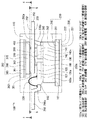
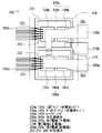
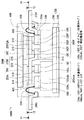
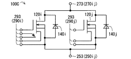
図1〜図5に、実施の形態1に係るパワー半導体モジュール100の構造図を示す。具体的には、図1はパワー半導体モジュール100の平面図(上面図)である。図2は図1中の矢印2の方向からパワー半導体モジュール100を見た場合の側面図であり、図3は図1中の矢印3の方向からパワー半導体モジュール100を見た場合の側面図である。図4は図2および図3中の4−4線の位置において矢印の方向からパワー半導体モジュール100を見た場合の平面図である。図5は図2および図3中の5−5線の位置において矢印の方向からパワー半導体モジュール100を見た場合の平面図である。なお、図2〜図5では、説明のために、後述のモールド樹脂(符号410参照。参考のためにその外形を二点鎖線で示す)を取り除いた状態を図示している。また、図6にパワー半導体モジュール100の回路図を示す。
図9〜図12に、実施の形態2に係るパワー半導体モジュール100Bの構造図を示す。具体的には、図9はパワー半導体モジュール100Bの平面図(上面図)である。図10は図9中の矢印10の方向からパワー半導体モジュール100Bを見た場合の側面図である。図11は図10中の11−11線の位置において矢印の方向からパワー半導体モジュール100Bを見た場合の平面図である。図12は図10中の12−12線の位置において矢印の方向からパワー半導体モジュール100Bを見た場合の平面図である。なお、図10〜図12では、説明のために、モールド樹脂410(参考のためにその外形を二点鎖線で示す)を取り除いた状態を図示している。また、図13にパワー半導体モジュール100Bの回路図を示す。
図16〜図19に、実施の形態3に係るパワー半導体モジュール100Cの構造図を示す。具体的には、図16はパワー半導体モジュール100Cの平面図(上面図)である。図17は図16中の矢印17の方向からパワー半導体モジュール100Cを見た場合の側面図である。図18は図17中の18−18線の位置において矢印の方向からパワー半導体モジュール100Cを見た場合の平面図である。図19は図17中の19−19線の位置において矢印の方向からパワー半導体モジュール100Cを見た場合の平面図である。なお、図17〜図19では、説明のために、モールド樹脂410(参考のためにその外形を二点鎖線で示す)を取り除いた状態を図示している。また、図20にパワー半導体モジュール100Cの回路図を示す。
図22〜図24に、実施の形態4に係るパワー半導体モジュール100Dの構造図を示す。具体的には、図22はパワー半導体モジュール100Dの平面図(上面図)である。図23は図22中の矢印23の方向からパワー半導体モジュール100Dを見た場合の側面図である。図24は図23中の24−24線の位置において矢印の方向からパワー半導体モジュール100Dを見た場合の平面図である。なお、上記の図4は、図23中の4−4線の位置において矢印の方向からパワー半導体モジュール100Dを見た場合の平面図としても利用される。
図25に、実施の形態5に係るパワー半導体モジュール100Eの側面図を示す。図25は図23に対応する。なお、上記の図4および図24は、図25中の4−4線および24−24線の位置において矢印の方向からパワー半導体モジュール100Eを見た場合の平面図としても利用される。
図26に、実施の形態6に係るパワー半導体モジュール100Fの側面図を示す。図26は図23に対応する。なお、上記の図4および図24は、図26中の4−4線および24−24線の位置において矢印の方向からパワー半導体モジュール100Fを見た場合の平面図としても利用される。
図27に、実施の形態7に係るパワー半導体モジュール100Gの側面図を示す。図27は図23に対応する。なお、上記の図4および図24は、図27中の4−4線および24−24線の位置において矢印の方向からパワー半導体モジュール100Gを見た場合の平面図としても利用される。
上記の実施の形態1等では、第3電極(副電極)290を有する構造を例示した。これに対し、第3電極290を必要としない半導体チップ(例えばダイオードチップ)のみを含んだパワー半導体モジュールでは、第3電極290は設けられない。
Claims (11)
- 樹脂封止型のパワー半導体モジュールであって、
それぞれが第1チップ主面および第2チップ主面を有する複数の半導体チップと、前記複数の半導体チップの前記第1チップ主面が第1接合部材によって接合された導電性を有するヒートスプレッダと、を含む単位構造体を複数備えると共に、
前記ヒートスプレッダから見て前記複数の半導体チップとは反対側に位置する絶縁部材と、
それぞれが第2接合部材によって所定箇所に接合された複数の主電極を含む複数の電極と
を備え、
前記複数の主電極は、
それぞれが前記複数の半導体チップのうちの所定のチップの前記第2チップ主面に前記第2接合部材によって接合された複数の第1電極と、
前記ヒートスプレッダのチップ搭載面に前記第2接合部材によって接合された第2電極と
を含み、
当該パワー半導体モジュールは、
前記複数の第1電極から見て前記複数の半導体チップとは反対側に位置する絶縁層と、前記絶縁層と前記複数の第1電極との間に位置し前記複数の第1電極に第3接合部材によって接合された第1導電層とを含む、絶縁基板と、
前記絶縁部材のうちで前記複数の半導体チップから遠い側の面と、前記絶縁基板のうちで前記複数の半導体チップから遠い側の面と、前記複数の電極の外部端子部分とが露出する状態で、前記複数の単位構造体と前記複数の電極を封止しているモールド樹脂と
を備え、
前記複数の電極は、当該複数の電極が予め形成されたリードフレームによって供給され、
前記複数の第1電極は、一の単位構造体において前記第2チップ主面に接合されていると共に他の単位構造体において前記ヒートスプレッダのチップ搭載面に接合されている直列接続型の第1電極を含み、
前記直列接続型の第1電極は、前記リードフレームから切り出された単一部材で構成されている、
パワー半導体モジュール。 - 前記複数の第1電極は前記絶縁基板の前記第1導電層に接合される面を同一平面上に有している、請求項1に記載のパワー半導体モジュール。
- 前記絶縁基板の前記第1導電層は複数の部分に分割されている、請求項1または請求項2に記載のパワー半導体モジュール。
- 前記第1導電層の前記複数の部分の個数は前記複数の第1電極の個数以上である、請求項3に記載のパワー半導体モジュール。
- 前記ヒートスプレッダから見て前記絶縁基板の側へ突出しているが前記絶縁基板に到達しない位置にループ頂点部を有する少なくとも1つのワイヤを更に備え、前記絶縁基板は前記少なくとも1つのワイヤの上方にも延在している、請求項1ないし請求項4のうちのいずれか1項に記載のパワー半導体モジュール。
- 前記絶縁基板は前記絶縁層から見て前記第1導電層とは反対側に第2導電層を更に含み、前記第1導電層は前記第2導電層よりも厚い、請求項1ないし請求項5のうちのいずれか1項に記載のパワー半導体モジュール。
- 前記複数の第1電極は、前記複数の半導体チップと接合する部分が前記複数の半導体チップと接合していない部分よりも厚い厚さ分布を有している、請求項1ないし請求項6のうちのいずれか1項に記載のパワー半導体モジュール。
- 前記第3接合部材は前記第1接合部材および前記第2接合部材よりも融点が低い、請求項1ないし請求項7のうちのいずれか1項に記載のパワー半導体モジュール。
- 前記複数の半導体チップは炭化珪素(SiC)を材料とする、請求項1ないし請求項8のうちのいずれか1項に記載のパワー半導体モジュール。
- 前記複数の第1電極は、前記モールド樹脂から外部へ突出して前記外部端子部分を有する突出型の第1電極を含み、
前記突出型の第1電極の前記外部端子部分と、前記第2電極の前記外部端子部分とは、前記絶縁部材の露出表面に平行な同一平面上に位置している、
請求項1ないし請求項9のうちのいずれか1項に記載のパワー半導体モジュール。 - 請求項1ないし請求項10のうちのいずれか1項に記載のパワー半導体モジュールを製造する方法であって、
(a)前記ヒートスプレッダ上に前記複数の半導体チップを前記第1接合部材によって接合する工程と、
(b)前記リードフレームに予め形成されている前記複数の電極のうちで前記第1電極を含む所定の電極群を、所定箇所に前記第2接合部材によって、同時に接合する工程と、
(c)前記モールド樹脂の形成後に前記リードフレームから前記パワー半導体モジュールを切り離す工程と
を備えるパワー半導体モジュールの製造方法。
Priority Applications (4)
| Application Number | Priority Date | Filing Date | Title |
|---|---|---|---|
| JP2012008083A JP5661052B2 (ja) | 2012-01-18 | 2012-01-18 | パワー半導体モジュールおよびその製造方法 |
| US13/617,048 US9059334B2 (en) | 2012-01-18 | 2012-09-14 | Power semiconductor module and method of manufacturing the same |
| CN201210385725.8A CN103219301B (zh) | 2012-01-18 | 2012-10-12 | 功率半导体模块及其制造方法 |
| DE102012222879.9A DE102012222879B4 (de) | 2012-01-18 | 2012-12-12 | Leistungshalbleitermodul und Verfahren zu seiner Herstellung |
Applications Claiming Priority (1)
| Application Number | Priority Date | Filing Date | Title |
|---|---|---|---|
| JP2012008083A JP5661052B2 (ja) | 2012-01-18 | 2012-01-18 | パワー半導体モジュールおよびその製造方法 |
Publications (3)
| Publication Number | Publication Date |
|---|---|
| JP2013149730A JP2013149730A (ja) | 2013-08-01 |
| JP2013149730A5 JP2013149730A5 (ja) | 2014-07-03 |
| JP5661052B2 true JP5661052B2 (ja) | 2015-01-28 |
Family
ID=48693298
Family Applications (1)
| Application Number | Title | Priority Date | Filing Date |
|---|---|---|---|
| JP2012008083A Active JP5661052B2 (ja) | 2012-01-18 | 2012-01-18 | パワー半導体モジュールおよびその製造方法 |
Country Status (4)
| Country | Link |
|---|---|
| US (1) | US9059334B2 (ja) |
| JP (1) | JP5661052B2 (ja) |
| CN (1) | CN103219301B (ja) |
| DE (1) | DE102012222879B4 (ja) |
Families Citing this family (33)
| Publication number | Priority date | Publication date | Assignee | Title |
|---|---|---|---|---|
| JP5542765B2 (ja) * | 2011-09-26 | 2014-07-09 | 日立オートモティブシステムズ株式会社 | パワーモジュール |
| DE102012101666B3 (de) * | 2012-02-29 | 2013-05-16 | Infineon Technologies Ag | Leistungshalbleitermodulsystem mit Hinterschneidungsverbindung |
| JP2013232495A (ja) * | 2012-04-27 | 2013-11-14 | Mitsubishi Electric Corp | 半導体装置 |
| WO2014054212A1 (ja) * | 2012-10-01 | 2014-04-10 | 富士電機株式会社 | 半導体装置とその製造方法 |
| JP5801339B2 (ja) * | 2013-03-22 | 2015-10-28 | 株式会社東芝 | 半導体装置 |
| JP5799974B2 (ja) * | 2013-05-23 | 2015-10-28 | 株式会社デンソー | 電子装置 |
| JP6303623B2 (ja) * | 2014-03-07 | 2018-04-04 | 富士電機株式会社 | 半導体装置、半導体装置の製造方法、位置決め治具 |
| JP6407756B2 (ja) * | 2014-03-31 | 2018-10-17 | 株式会社東芝 | 半導体モジュールの製造方法 |
| DE102014106686B4 (de) * | 2014-05-12 | 2022-12-01 | Infineon Technologies Austria Ag | Elektronisches modul, elektronisches system und verfahren zum herstellen desselben |
| JP6227150B2 (ja) * | 2014-08-29 | 2017-11-08 | 三菱電機株式会社 | 半導体装置及び多相用半導体装置 |
| JP6429889B2 (ja) * | 2014-09-25 | 2018-11-28 | 日立オートモティブシステムズ株式会社 | 電力変換装置 |
| JP6293030B2 (ja) * | 2014-10-09 | 2018-03-14 | 三菱電機株式会社 | 電力用半導体装置 |
| JP6345265B2 (ja) * | 2014-10-29 | 2018-06-20 | 日立オートモティブシステムズ株式会社 | 電子機器及び電子機器の製造方法 |
| CN107210238B (zh) * | 2015-02-25 | 2020-03-17 | 三菱电机株式会社 | 功率模块 |
| CN108496247B (zh) | 2016-01-29 | 2022-05-17 | 三菱电机株式会社 | 半导体装置 |
| KR101786343B1 (ko) * | 2016-05-04 | 2017-10-18 | 현대자동차주식회사 | 양면냉각형 파워모듈 |
| DE102016120778B4 (de) * | 2016-10-31 | 2024-01-25 | Infineon Technologies Ag | Baugruppe mit vertikal beabstandeten, teilweise verkapselten Kontaktstrukturen |
| US10074590B1 (en) * | 2017-07-02 | 2018-09-11 | Infineon Technologies Ag | Molded package with chip carrier comprising brazed electrically conductive layers |
| JP2019057576A (ja) | 2017-09-20 | 2019-04-11 | ルネサスエレクトロニクス株式会社 | 半導体装置 |
| US10453777B2 (en) * | 2018-01-30 | 2019-10-22 | Toyota Motor Engineering & Manufacturing North America, Inc. | Power electronics assemblies with cio bonding layers and double sided cooling, and vehicles incorporating the same |
| KR20210018811A (ko) * | 2018-05-29 | 2021-02-18 | 에이펙스 마이크로테크놀로지, 인코포레이티드 | 열 전도성 전자장치 패키징 |
| JP7010167B2 (ja) * | 2018-07-25 | 2022-01-26 | 株式会社デンソー | 半導体装置 |
| JP7155990B2 (ja) * | 2018-12-17 | 2022-10-19 | 株式会社デンソー | 半導体モジュール |
| US11682606B2 (en) * | 2019-02-07 | 2023-06-20 | Ford Global Technologies, Llc | Semiconductor with integrated electrically conductive cooling channels |
| JP7059970B2 (ja) * | 2019-03-11 | 2022-04-26 | 株式会社デンソー | 半導体装置 |
| JP2021057534A (ja) * | 2019-10-01 | 2021-04-08 | 株式会社デンソー | 半導体装置 |
| EP3869923A1 (en) * | 2020-02-20 | 2021-08-25 | AT & S Austria Technologie & Systemtechnik Aktiengesellschaft | Cooling profile integration for embedded power systems |
| US11721617B2 (en) | 2020-04-07 | 2023-08-08 | Wolfspeed, Inc. | Power module |
| US11735488B2 (en) | 2020-04-07 | 2023-08-22 | Wolfspeed, Inc. | Power module |
| US11373941B2 (en) * | 2020-10-12 | 2022-06-28 | Renesas Electronics Corporation | Sense MOSFET electrically connected to a source pad via a plurality of source extraction ports |
| JP2022181816A (ja) * | 2021-05-27 | 2022-12-08 | 株式会社デンソー | 半導体装置 |
| DE102022207269A1 (de) | 2022-07-18 | 2024-01-18 | Zf Friedrichshafen Ag | Verfahren und Vorrichtung zum Herstellen einer Anschlussvorrichtung zum Anschließen zumindest eines elektrischen oder elektronischen Bauteils für ein elektrisches oder elektronisches Modul |
| DE102022207270A1 (de) | 2022-07-18 | 2024-01-18 | Zf Friedrichshafen Ag | Verfahren und Vorrichtung zum Herstellen einer Anschlussvorrichtung zum Anschließen zumindest eines elektrischen oder elektronischen Bauteils für ein elektrisches oder elektronisches Modul |
Family Cites Families (19)
| Publication number | Priority date | Publication date | Assignee | Title |
|---|---|---|---|---|
| JP3879150B2 (ja) * | 1996-08-12 | 2007-02-07 | 株式会社デンソー | 半導体装置 |
| US6072240A (en) * | 1998-10-16 | 2000-06-06 | Denso Corporation | Semiconductor chip package |
| US6693350B2 (en) * | 1999-11-24 | 2004-02-17 | Denso Corporation | Semiconductor device having radiation structure and method for manufacturing semiconductor device having radiation structure |
| US6703707B1 (en) * | 1999-11-24 | 2004-03-09 | Denso Corporation | Semiconductor device having radiation structure |
| JP4044265B2 (ja) * | 2000-05-16 | 2008-02-06 | 三菱電機株式会社 | パワーモジュール |
| JP4338620B2 (ja) * | 2004-11-01 | 2009-10-07 | 三菱電機株式会社 | 半導体装置及びその製造方法 |
| JP2007184525A (ja) * | 2005-12-07 | 2007-07-19 | Mitsubishi Electric Corp | 電子機器装置 |
| JP4450230B2 (ja) * | 2005-12-26 | 2010-04-14 | 株式会社デンソー | 半導体装置 |
| JP2007251076A (ja) | 2006-03-20 | 2007-09-27 | Hitachi Ltd | パワー半導体モジュール |
| JP2007311518A (ja) * | 2006-05-18 | 2007-11-29 | Mitsubishi Electric Corp | 半導体装置の製造方法及び半導体装置 |
| JP2008041752A (ja) | 2006-08-02 | 2008-02-21 | Hitachi Metals Ltd | 半導体モジュールおよび半導体モジュール用放熱板 |
| US7999369B2 (en) * | 2006-08-29 | 2011-08-16 | Denso Corporation | Power electronic package having two substrates with multiple semiconductor chips and electronic components |
| CN101136396B (zh) | 2006-08-30 | 2011-08-10 | 株式会社电装 | 包括两片带有多个半导体芯片和电子元件的衬底的功率电子封装件 |
| JP5076440B2 (ja) | 2006-10-16 | 2012-11-21 | 富士電機株式会社 | 半導体装置及び半導体装置の製造方法 |
| JP4748173B2 (ja) | 2008-03-04 | 2011-08-17 | 株式会社デンソー | 半導体モジュール及びその製造方法 |
| JP2009224560A (ja) | 2008-03-17 | 2009-10-01 | Denso Corp | 半導体装置およびその製造方法 |
| JP2010239033A (ja) | 2009-03-31 | 2010-10-21 | Honda Motor Co Ltd | 半導体装置及びその製造方法 |
| JP2011216564A (ja) * | 2010-03-31 | 2011-10-27 | Mitsubishi Electric Corp | パワーモジュール及びその製造方法 |
| JP5253455B2 (ja) | 2010-06-01 | 2013-07-31 | 三菱電機株式会社 | パワー半導体装置 |
-
2012
- 2012-01-18 JP JP2012008083A patent/JP5661052B2/ja active Active
- 2012-09-14 US US13/617,048 patent/US9059334B2/en active Active
- 2012-10-12 CN CN201210385725.8A patent/CN103219301B/zh active Active
- 2012-12-12 DE DE102012222879.9A patent/DE102012222879B4/de active Active
Also Published As
| Publication number | Publication date |
|---|---|
| CN103219301A (zh) | 2013-07-24 |
| JP2013149730A (ja) | 2013-08-01 |
| DE102012222879B4 (de) | 2023-05-04 |
| CN103219301B (zh) | 2016-01-20 |
| US20130181228A1 (en) | 2013-07-18 |
| US9059334B2 (en) | 2015-06-16 |
| DE102012222879A1 (de) | 2013-07-18 |
Similar Documents
| Publication | Publication Date | Title |
|---|---|---|
| JP5661052B2 (ja) | パワー半導体モジュールおよびその製造方法 | |
| JP5232367B2 (ja) | 半導体装置 | |
| TWI505444B (zh) | Semiconductor device | |
| US7514780B2 (en) | Power semiconductor device | |
| EP3107120B1 (en) | Power semiconductor module | |
| US20160005675A1 (en) | Double sided cooling chip package and method of manufacturing the same | |
| US9099426B2 (en) | Trench-assisted thermoelectric isothermalization of power switching chips | |
| US9831160B2 (en) | Semiconductor device | |
| WO2010147202A1 (ja) | 電力変換装置 | |
| US11776867B2 (en) | Chip package | |
| US10483237B2 (en) | Vertically stacked multichip modules | |
| CN103996667B (zh) | 具有旁路功能的半导体器件及其方法 | |
| JP2013179229A (ja) | パワーモジュール半導体装置 | |
| US11862542B2 (en) | Dual side cooling power module and manufacturing method of the same | |
| US20060055056A1 (en) | Semiconductor equipment having a pair of heat radiation plates | |
| JP2013062282A (ja) | 半導体装置 | |
| JP2017054842A (ja) | 配線基板、半導体装置、及び半導体パッケージ | |
| JP2005286187A (ja) | 半導体装置 | |
| CN110676232B (zh) | 一种半导体器件封装结构及其制作方法、一种电子设备 | |
| CN111524877B (zh) | 一种双面散热功率模块 | |
| JP2017054855A (ja) | 半導体装置、及び半導体パッケージ | |
| US11532534B2 (en) | Semiconductor module | |
| US11276627B2 (en) | Semiconductor device | |
| JP7294403B2 (ja) | 半導体装置 | |
| JP2010062492A (ja) | 半導体装置 |
Legal Events
| Date | Code | Title | Description |
|---|---|---|---|
| A521 | Request for written amendment filed |
Free format text: JAPANESE INTERMEDIATE CODE: A523 Effective date: 20140519 |
|
| A621 | Written request for application examination |
Free format text: JAPANESE INTERMEDIATE CODE: A621 Effective date: 20140519 |
|
| A977 | Report on retrieval |
Free format text: JAPANESE INTERMEDIATE CODE: A971007 Effective date: 20140827 |
|
| A131 | Notification of reasons for refusal |
Free format text: JAPANESE INTERMEDIATE CODE: A131 Effective date: 20140909 |
|
| A521 | Request for written amendment filed |
Free format text: JAPANESE INTERMEDIATE CODE: A523 Effective date: 20141008 |
|
| TRDD | Decision of grant or rejection written | ||
| A01 | Written decision to grant a patent or to grant a registration (utility model) |
Free format text: JAPANESE INTERMEDIATE CODE: A01 Effective date: 20141104 |
|
| A61 | First payment of annual fees (during grant procedure) |
Free format text: JAPANESE INTERMEDIATE CODE: A61 Effective date: 20141202 |
|
| R150 | Certificate of patent or registration of utility model |
Ref document number: 5661052 Country of ref document: JP Free format text: JAPANESE INTERMEDIATE CODE: R150 |
|
| R250 | Receipt of annual fees |
Free format text: JAPANESE INTERMEDIATE CODE: R250 |
|
| R250 | Receipt of annual fees |
Free format text: JAPANESE INTERMEDIATE CODE: R250 |
|
| R250 | Receipt of annual fees |
Free format text: JAPANESE INTERMEDIATE CODE: R250 |
|
| R250 | Receipt of annual fees |
Free format text: JAPANESE INTERMEDIATE CODE: R250 |
|
| R250 | Receipt of annual fees |
Free format text: JAPANESE INTERMEDIATE CODE: R250 |
|
| R250 | Receipt of annual fees |
Free format text: JAPANESE INTERMEDIATE CODE: R250 |
|
| R250 | Receipt of annual fees |
Free format text: JAPANESE INTERMEDIATE CODE: R250 |