WO2016047184A1 - 成膜方法およびスパッタリング装置 - Google Patents
成膜方法およびスパッタリング装置 Download PDFInfo
- Publication number
- WO2016047184A1 WO2016047184A1 PCT/JP2015/061238 JP2015061238W WO2016047184A1 WO 2016047184 A1 WO2016047184 A1 WO 2016047184A1 JP 2015061238 W JP2015061238 W JP 2015061238W WO 2016047184 A1 WO2016047184 A1 WO 2016047184A1
- Authority
- WO
- WIPO (PCT)
- Prior art keywords
- target
- frequency power
- antenna
- plasma
- sputtering
- Prior art date
- Legal status (The legal status is an assumption and is not a legal conclusion. Google has not performed a legal analysis and makes no representation as to the accuracy of the status listed.)
- Ceased
Links
Images


Classifications
-
- C—CHEMISTRY; METALLURGY
- C23—COATING METALLIC MATERIAL; COATING MATERIAL WITH METALLIC MATERIAL; CHEMICAL SURFACE TREATMENT; DIFFUSION TREATMENT OF METALLIC MATERIAL; COATING BY VACUUM EVAPORATION, BY SPUTTERING, BY ION IMPLANTATION OR BY CHEMICAL VAPOUR DEPOSITION, IN GENERAL; INHIBITING CORROSION OF METALLIC MATERIAL OR INCRUSTATION IN GENERAL
- C23C—COATING METALLIC MATERIAL; COATING MATERIAL WITH METALLIC MATERIAL; SURFACE TREATMENT OF METALLIC MATERIAL BY DIFFUSION INTO THE SURFACE, BY CHEMICAL CONVERSION OR SUBSTITUTION; COATING BY VACUUM EVAPORATION, BY SPUTTERING, BY ION IMPLANTATION OR BY CHEMICAL VAPOUR DEPOSITION, IN GENERAL
- C23C14/00—Coating by vacuum evaporation, by sputtering or by ion implantation of the coating forming material
- C23C14/22—Coating by vacuum evaporation, by sputtering or by ion implantation of the coating forming material characterised by the process of coating
- C23C14/34—Sputtering
- C23C14/3471—Introduction of auxiliary energy into the plasma
-
- C—CHEMISTRY; METALLURGY
- C23—COATING METALLIC MATERIAL; COATING MATERIAL WITH METALLIC MATERIAL; CHEMICAL SURFACE TREATMENT; DIFFUSION TREATMENT OF METALLIC MATERIAL; COATING BY VACUUM EVAPORATION, BY SPUTTERING, BY ION IMPLANTATION OR BY CHEMICAL VAPOUR DEPOSITION, IN GENERAL; INHIBITING CORROSION OF METALLIC MATERIAL OR INCRUSTATION IN GENERAL
- C23C—COATING METALLIC MATERIAL; COATING MATERIAL WITH METALLIC MATERIAL; SURFACE TREATMENT OF METALLIC MATERIAL BY DIFFUSION INTO THE SURFACE, BY CHEMICAL CONVERSION OR SUBSTITUTION; COATING BY VACUUM EVAPORATION, BY SPUTTERING, BY ION IMPLANTATION OR BY CHEMICAL VAPOUR DEPOSITION, IN GENERAL
- C23C14/00—Coating by vacuum evaporation, by sputtering or by ion implantation of the coating forming material
- C23C14/22—Coating by vacuum evaporation, by sputtering or by ion implantation of the coating forming material characterised by the process of coating
- C23C14/34—Sputtering
-
- H—ELECTRICITY
- H01—ELECTRIC ELEMENTS
- H01J—ELECTRIC DISCHARGE TUBES OR DISCHARGE LAMPS
- H01J37/00—Discharge tubes with provision for introducing objects or material to be exposed to the discharge, e.g. for the purpose of examination or processing thereof
- H01J37/32—Gas-filled discharge tubes
- H01J37/34—Gas-filled discharge tubes operating with cathodic sputtering
- H01J37/3402—Gas-filled discharge tubes operating with cathodic sputtering using supplementary magnetic fields
- H01J37/3405—Magnetron sputtering
- H01J37/3408—Planar magnetron sputtering
-
- H—ELECTRICITY
- H01—ELECTRIC ELEMENTS
- H01J—ELECTRIC DISCHARGE TUBES OR DISCHARGE LAMPS
- H01J37/00—Discharge tubes with provision for introducing objects or material to be exposed to the discharge, e.g. for the purpose of examination or processing thereof
- H01J37/32—Gas-filled discharge tubes
- H01J37/34—Gas-filled discharge tubes operating with cathodic sputtering
- H01J37/3411—Constructional aspects of the reactor
- H01J37/3444—Associated circuits
-
- H—ELECTRICITY
- H05—ELECTRIC TECHNIQUES NOT OTHERWISE PROVIDED FOR
- H05H—PLASMA TECHNIQUE; PRODUCTION OF ACCELERATED ELECTRICALLY-CHARGED PARTICLES OR OF NEUTRONS; PRODUCTION OR ACCELERATION OF NEUTRAL MOLECULAR OR ATOMIC BEAMS
- H05H1/00—Generating plasma; Handling plasma
- H05H1/24—Generating plasma
- H05H1/46—Generating plasma using applied electromagnetic fields, e.g. high frequency or microwave energy
Definitions
- the present invention relates to a film forming method and a sputtering apparatus for forming a film on a substrate by sputtering (in other words, film formation; the same applies hereinafter), and more specifically, an inductively coupled plasma by supplying high-frequency power to an antenna.
- the present invention relates to a film forming method and a sputtering apparatus that generate (abbreviated ICP) to sputter a target.
- IGZO In-Ga-Zn-O / indium-gallium-zinc-oxygen
- ITZO In-Sn-Zn-O / indium-tin-zinc-
- Oxide semiconductors such as oxygen
- Such an oxide semiconductor thin film for TFT often uses a magnetron discharge in which an electric field and a magnetic field are orthogonal to each other, and allows electrons emitted from the cathode to move along a continuous locus in the vicinity of the target.
- a heterogeneous film for example, a film having a varied film composition, etc.
- Non-Patent Document 1 and Patent Document 1 a cathode including a target (this is called a target device in Patent Document 1) is made movable.
- An improved film forming method and sputtering apparatus have been proposed that enable plasma lighting and plasma extinguishing at positions where the target and the substrate do not face each other and suppress unstable film formation during plasma lighting and plasma extinguishing. ing.
- Non-Patent Document 1 and Patent Document 1 in addition to a target as a film forming material, a high voltage for sputtering (for example, about ⁇ 1 kV) is applied to the target for the movable cathode.
- a high voltage for sputtering for example, about ⁇ 1 kV
- high frequency power is supplied to an antenna provided in a vacuum vessel into which a sputtering gas is introduced to generate inductively coupled plasma, which is applied to the plasma and a target.
- a sputtering apparatus for forming a film on a substrate by sputtering a target using a target bias voltage
- the high frequency power is supplied to the antenna and the plasma is generated.
- Sputtering was started by applying the target bias voltage to the target.
- the target bias voltage applied to the target was stopped and sputtering was stopped, and then the antenna was supplied to the antenna.
- the high frequency power is stopped to extinguish the plasma.
- the high frequency power is supplied to the antenna to generate the plasma, and then the target bias voltage applied to the target is gradually increased from zero to a predetermined value. After the target bias voltage applied to the target is gradually reduced and stopped, the high frequency power supplied to the antenna may be stopped to extinguish the plasma.
- the high frequency power supplied to the antenna is gradually increased to generate the plasma with the minimum power, and then the target bias voltage is applied to the target, and then the antenna
- the high-frequency power supplied to the battery may be gradually increased to a predetermined value.
- a sputtering apparatus generates an inductively coupled plasma by supplying a high frequency power from a high frequency power source to an antenna provided in a vacuum vessel into which a sputtering gas is introduced, and the plasma and a target bias power source
- a sputtering apparatus that forms a film on a substrate by sputtering the target using a target bias voltage applied to the target from the target, and controls the high-frequency power source and the target bias power source, and (a) film formation A function of starting the sputtering by applying the target bias voltage to the target from the target bias power source after generating the plasma by supplying the high frequency power from the high frequency power source to the antenna at the start of b)
- the target buy A control having a function of stopping the high frequency power supplied to the antenna and extinguishing the plasma after stopping the target bias voltage applied to the target from the power source and stopping the sputtering. It is characterized by having a device.
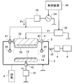
- the gas 10 is introduced into the vacuum vessel 2.
- the gas is introduced from the gas source 6 via the flow rate regulator 8.
- the gas 10 is, for example, argon gas.
- the gas 10 may be a mixed gas of argon gas and active gas (for example, oxygen gas, nitrogen gas, etc.).
- a substrate holder 14 for holding a substrate 12 on which a thin film is formed is provided in the vacuum vessel 2.
- the substrate bias voltage V S may be applied to the substrate holder 14 from the substrate bias power supply 16.
- the substrate bias voltage V S may be a negative DC voltage, a negative pulse voltage, an AC voltage, or the like.
- Reference numeral 40 denotes an insulating part having a vacuum sealing function.
- the target bias voltage V T output from the target bias power supply 34 may be determined according to, for example, the material of the target 30.
- the negative DC voltage shown in the above (a) may be used, or the voltages shown in (b) and (c) may be used.
- the positive and negative alternating pulse voltages shown in (b) above or the AC voltage shown in (c) above may be used. By doing so, it is possible to prevent the surface of the insulator from being covered with the positive charge of the inflowing ions to stop the sputtering.
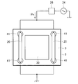
- the antenna 20 is disposed in the vacuum container 2 and in the vicinity of the surface of the target 30. More specifically, in this example, the two antennas 20 are respectively disposed along opposite sides of the quadrangular target 30 so as to sandwich the target 30 from both sides.
- each antenna 20 is preferably arranged along the long side of the target 30.
- each antenna 20 is a rod-like conductor having a shape that is straight (i.e., linear) except for both ends, and both ends are bent upward and penetrate the upper surface portion 3 of the vacuum vessel 2. A part protrudes on the upper surface part 3. The penetration part is provided with an insulating part 41 having a vacuum sealing function.
- Each antenna 20, in this example, the high frequency power P R is supplied in parallel from the high frequency power source 24 via a matching circuit 26. More specifically, the matching circuit 26 is connected to one end of each antenna 20, and the other end of each antenna 20 is grounded. One end of the high frequency power supply 24 is also grounded. However, a high frequency power supply 24 and a matching circuit 26 may be provided for each antenna 20. Frequency of the high frequency power P R output from the high frequency power source 24 is, for example, is a common 13.56 MHz, the invention is not limited thereto.
- the surface of the target 30 can be more uniformly sputtered and the surface can be used more uniformly.
- the two antennas 20 may be arranged along one side of the target 30.
- Each antenna 20 may have a solid structure, or a cooling water channel may be provided inside, for example, each antenna 20 may be tubular or cylindrical, and each antenna 20 may be flowed through each antenna 20 by flowing cooling water. You may make it the water-cooling structure to cool.
- This sputtering apparatus further includes a control device 46 for controlling the high frequency power supply 24 and the target bias power supply 34.
- the control device 46 will be described later.
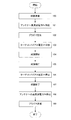
- step 100 film formation is prepared (step 100). Specifically, the substrate 12 on which a thin film is to be formed is placed on the substrate holder 14 in the vacuum vessel 2, the inside of the vacuum vessel 2 is evacuated by the evacuation device 4, and a sputtering gas is placed in the vacuum vessel 2. 10 is introduced and the inside of the vacuum vessel 2 is maintained at a predetermined pressure.
- This pressure may be set within a range in which the plasma 22 can be easily generated and a film having excellent characteristics can be formed on the substrate 12. For example, it may be about 0.1 Pa to 10 Pa, more specifically about 1 Pa to 3 Pa. More specifically, the substrate bias voltage V S may be applied to the substrate 12 from the substrate bias power supply 16 as needed to the substrate holder 14.
- step 101 From the high frequency power source 24 to each antenna 20 to supply high frequency power P R (step 101) to generate an inductively coupled plasma 22 in a vacuum chamber 2 (step 102). That is, by supplying a high frequency power P R to each antenna 20, a high-frequency current flows through each antenna 20, thereby high-frequency magnetic field is generated around each antenna 20, the induced electric field whereby the high frequency current in the opposite direction appear. Due to this induced electric field, electrons are accelerated in the vacuum chamber 2 to ionize the gas 10 in the vicinity of the antenna 20 and generate plasma 22 in the vicinity of the antenna 20. Since this method is inductively coupled plasma generation, high-density plasma 22 can be generated.
- the target bias voltage V T that attracts ions in the plasma 22 is not applied to the target 30, the target 30 is not sputtered despite the high-density plasma 22. . That is, film formation on the substrate 12 is not performed.
- a target bias voltage V T is applied to the target 30 from the target bias power supply 34 (step 103), and the target 30 is moved by ions in the plasma 22.
- Sputtering is performed to start film formation on the substrate 12 (step 104). Further, the film formation is continued for a desired time (step 105). This increases the film thickness of the thin film formed on the substrate 12.
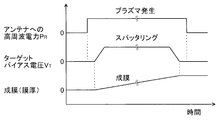
- the predetermined time t 1 is a time to wait until the plasma 22 is stabilized when the plasma is turned on. If the time is too short, the plasma 22 may not be stable yet. If the time is too long, the throughput decreases. It is preferably within the range of about 60 seconds, and more preferably within the range of about 5 seconds to 30 seconds.
- the target bias voltage V T applied to the target 30 is stopped to stop sputtering (step 106), and film formation on the substrate 12 is ended (step 107). Then, for example, after a predetermined time t 2 from the sputtering stop (see FIG. 5), to stop the high frequency power P R which has been supplied to the antenna 20 (step 108), extinguish the plasma 22 (step 109). Thus, the film forming process for the substrate 12 is completed.
- the predetermined time t 2 is a time for waiting for the influence of the target bias voltage V T applied to the target 30 to completely disappear when the target bias voltage V T is stopped. If the time is too short, the influence of the target bias voltage V T remains. If the length is too long, the throughput decreases. For example, it is preferably in the range of about 1 second to 10 seconds, and more preferably in the range of about 2 seconds to 5 seconds.
- the above film forming method at the start of the film formation, after plasma is generated 22 by supplying a high frequency power P R to the antenna 20, to start the sputtering by applying a target bias voltage V T to the target 30 Therefore, it is possible to avoid film formation when the plasma 22 is unstable when the plasma is turned on. Accordingly, it is possible to suppress the formation of a heterogeneous film (for example, a film having a varied film composition; the same applies hereinafter) on the substrate 12 at the start of film formation.
- a heterogeneous film for example, a film having a varied film composition; the same applies hereinafter
- the above-described effects can be achieved without providing a target moving mechanism. That is, it is not necessary to provide a cathode moving mechanism including a target as described in Non-Patent Document 1 or a target moving mechanism as described in Patent Document 1. Therefore, since the apparatus configuration can be simplified as compared with the case where a target moving mechanism is provided, the cause of trouble can be reduced and the cost of the apparatus can be reduced.
- high-density plasma 22 can be generated in the vicinity of the surface of the target 30 by inductively coupled plasma generation, so that the surface of the target 30 is wider than that of the magnetron sputtering method.
- the magnetron sputtering method only a specific region where the electric field and the magnetic field are orthogonal to each other is cut into a donut shape, whereas in the case of this film forming method, there is no such limitation. Therefore, the utilization efficiency of the target 30 can be increased.
- the sputtering apparatus includes a control device 46 having a function of controlling the high-frequency power source 24 and the target bias power source 34 to perform the film forming method. More specifically, the control device 46 in this example, at the start of (a) deposition, by supplying a high-frequency power P R after generating the plasma 22 to the antenna 20 from the high frequency power source 24, the target bias power source 34 A function of applying a target bias voltage V T to the target 30 to start sputtering, and (b) at the end of film formation, the target bias voltage V T applied to the target 30 from the target bias power supply 34 is stopped and sputtering is performed. the after stopping, and a function to stop the high frequency power P R which has been supplied to the antenna 20 the plasma is extinguished 22.
- the sputtering apparatus can achieve the same effects as the effects provided by the film forming method.
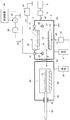
- FIG. 6 shows a more specific example of a sputtering apparatus for performing the film forming method according to the present invention. In the following, differences from the above-described example will be mainly described.
- This sputtering apparatus has a structure in which a load lock chamber 54 is connected to a vacuum vessel 2 (hereinafter referred to as a film forming chamber 50) of the sputtering apparatus shown in FIG. ing.
- the case where an oxide semiconductor thin film is formed on the glass substrate 12 will be described as an example.
- the substrate 12 is placed on the substrate holder 58 in the load lock chamber 54 through the door 64 from the atmosphere, the substrate 12 is loaded by the vacuum exhaust device 56.
- the lock chamber 54 is evacuated to a predetermined degree of vacuum (for example, 5 ⁇ 10 ⁇ 5 Pa or less).
- the inside of the film forming chamber 50 is also evacuated to the same extent by the evacuation apparatus 4.
- the gate valve 52 is opened, and the substrate transfer device 60 transfers the substrate 12 from the load lock chamber 54 to the film formation chamber 50 as indicated by the arrow A and places it on the substrate holder 14.
- a vacuum seal portion 62 such as a bellows is provided at a portion where the substrate transfer device 60 penetrates the wall surface of the load lock chamber 54.
- the film forming chamber 50 is evacuated to a predetermined degree of vacuum (for example, 5 ⁇ 10 ⁇ 5 Pa or less) by the vacuum evacuation device 4, and then the gas 10 whose flow rate is adjusted by the flow rate regulator 8 is introduced. Then, the inside of the film forming chamber 50 is maintained at a predetermined pressure (for example, about 1 Pa to 3 Pa as described above).
- the gas 10 to be introduced is, for example, argon gas, but may be a mixed gas of argon and oxygen.
- the material of the target 30 is, for example, the aforementioned IGZO (In (-Ga -Zn -O). As a result, an IGZO film can be formed on the glass substrate 12.
- the plasma 22 is extinguished (see step 109 in FIG. 4), and the supply of the gas 10 is stopped. -5 Pa or less).
- the inside of the load lock chamber 54 is also evacuated to the same extent by the evacuation device 56.
- the gate valve 52 is opened, and the substrate transport apparatus 60 transports the film-formed substrate 12 from the film formation chamber 50 to the load lock chamber 54 as indicated by the arrow A and places it on the substrate holder 58.
- the gate valve 52 is closed, the inside of the load lock chamber 54 is returned to the atmospheric pressure state (that is, after leakage or venting), and then the substrate 12 is taken out into the atmosphere through the door 64.
- the atmospheric pressure state that is, after leakage or venting
- planar shape of the target 30 may be other than the above-described quadrangle (square or rectangle).
- it may be circular.
- the shape of the heel antenna 20 is not limited to a linear shape except for the both end portions described above, and other shapes may be used.
- the shape of the antenna 20 may be linear as a whole, or may be U-shaped, U-shaped, coiled, or the like.
- the shape according to the planar shape of the target 30 may be sufficient.
- the planar shape of the antenna 20 may be circular.
- the antenna 20 may be an antenna having the following structure described in Japanese Patent Application Laid-Open No. 2013-206652. That is, the antenna 20 has an inner conductor, an outer conductor that covers at least the entire length of the inner conductor, and a dielectric that is provided between the inner conductor and the outer conductor to electrically insulate between the two conductors. It may have a coaxial structure and may have a water cooling structure in which cooling water is allowed to flow inside at least one of the inner conductor and the outer conductor to cool the antenna. A high frequency power source is connected to one end of the inner conductor of the antenna via a matching circuit, and the other end of the inner conductor is grounded.
- the outer conductor is made of a nonmagnetic material, and the outer conductor is grounded only at one end thereof.
- a film forming method of extinguishing the plasma 22 may be employed.
- the pattern in which the target bias voltage V T is gradually raised or lowered may be curved instead of the straight line as shown in FIG.
- the target bias voltage V T applied to the target 30 is disturbed by transients, it is conceivable that disturbed quality to be formed therebetween
- the target bias voltage V T is gradually increased at the beginning of film formation and gradually decreased at the end of film formation as in this film formation method, thereby suppressing disturbance of the target bias voltage V T due to a transient phenomenon. Therefore, the disturbance of the film quality due to the disturbance of the target bias voltage V T as described above can be suppressed. Therefore, the effect of suppressing the formation of a heterogeneous film at the start and end of film formation can be enhanced.
- the control device 46 described above constitute a sputtering apparatus, at the start of (a) deposition, and supplying high-frequency power P R from the high frequency power source 24 to the antenna 20 A function of gradually increasing the target bias voltage V T applied from the target bias power source 34 to the target 30 from zero to a predetermined value after the plasma 22 is generated, and (b) at the end of film formation, the target bias power source 34 from after stopping gradually reduced target bias voltage V T which has been applied to the target 30, further a function of stopping the high-frequency power P R, which has been supplied from the high frequency power source 24 to the antenna 20 to extinguish plasma 22 You may have.
- the sputtering apparatus provided with such a control device 46 can achieve the same effects as the above-described effects provided by the film forming method.
- the high frequency power P R after the target bias voltage V T is stopped and the sputtering is stopped may be stopped at once as in the example shown in FIG. 8, or may be stopped after being gradually reduced.
- the control device 46 described above constitute a sputtering apparatus, at the start of the film formation, gradually increase the high frequency power P R is supplied from the high frequency power source 24 to the antenna 20 after generating the plasma 22 at minimum power and, by applying a target bias voltage V T to the target 30 from the target bias power source 34, then further, from the high frequency power source 24 a high-frequency power P R is supplied to the antenna 20 to a predetermined value You may further have the function to enlarge gradually.
- the sputtering apparatus provided with such a control device 46 can achieve the same effects as the above-described effects provided by the film forming method.
- Vacuum container 10 Gas 12 Substrate 20 Antenna 22 Plasma 24 High frequency power supply 30 Target 34 Target bias power supply 46 Controller PR High frequency power V T Target bias voltage
Landscapes
- Chemical & Material Sciences (AREA)
- Engineering & Computer Science (AREA)
- Physics & Mathematics (AREA)
- Plasma & Fusion (AREA)
- Mechanical Engineering (AREA)
- Materials Engineering (AREA)
- Chemical Kinetics & Catalysis (AREA)
- Metallurgy (AREA)
- Organic Chemistry (AREA)
- Analytical Chemistry (AREA)
- Electromagnetism (AREA)
- Spectroscopy & Molecular Physics (AREA)
- Physical Vapour Deposition (AREA)
- Plasma Technology (AREA)
- Physical Deposition Of Substances That Are Components Of Semiconductor Devices (AREA)
Priority Applications (2)
| Application Number | Priority Date | Filing Date | Title |
|---|---|---|---|
| KR1020177010896A KR20170058428A (ko) | 2014-09-26 | 2015-04-10 | 성막 방법 및 스퍼터링 장치 |
| CN201580051441.7A CN106715750B (zh) | 2014-09-26 | 2015-04-10 | 成膜方法及溅镀装置 |
Applications Claiming Priority (2)
| Application Number | Priority Date | Filing Date | Title |
|---|---|---|---|
| JP2014-196266 | 2014-09-26 | ||
| JP2014196266A JP6264248B2 (ja) | 2014-09-26 | 2014-09-26 | 成膜方法およびスパッタリング装置 |
Publications (1)
| Publication Number | Publication Date |
|---|---|
| WO2016047184A1 true WO2016047184A1 (ja) | 2016-03-31 |
Family
ID=55580725
Family Applications (1)
| Application Number | Title | Priority Date | Filing Date |
|---|---|---|---|
| PCT/JP2015/061238 Ceased WO2016047184A1 (ja) | 2014-09-26 | 2015-04-10 | 成膜方法およびスパッタリング装置 |
Country Status (4)
| Country | Link |
|---|---|
| JP (1) | JP6264248B2 (enExample) |
| KR (1) | KR20170058428A (enExample) |
| CN (1) | CN106715750B (enExample) |
| WO (1) | WO2016047184A1 (enExample) |
Cited By (2)
| Publication number | Priority date | Publication date | Assignee | Title |
|---|---|---|---|---|
| GB2597985A (en) * | 2020-08-13 | 2022-02-16 | Dyson Technology Ltd | Method of forming a cathode layer, method of forming a battery half cell |
| US11328913B2 (en) | 2017-03-17 | 2022-05-10 | Nissin Electric Co., Ltd. | Sputtering device |
Families Citing this family (9)
| Publication number | Priority date | Publication date | Assignee | Title |
|---|---|---|---|---|
| TWI684283B (zh) * | 2017-06-07 | 2020-02-01 | 日商日新電機股份有限公司 | 薄膜電晶體的製造方法 |
| JP6310601B1 (ja) | 2017-06-07 | 2018-04-11 | 日新電機株式会社 | スパッタリング装置 |
| JP6916699B2 (ja) * | 2017-09-14 | 2021-08-11 | 株式会社Screenホールディングス | 成膜方法および成膜装置 |
| CN111542645B (zh) | 2017-12-27 | 2022-07-26 | 佳能安内华股份有限公司 | 成膜方法及成膜装置 |
| JP2021088727A (ja) * | 2018-03-20 | 2021-06-10 | 日新電機株式会社 | 成膜方法 |
| CN111270209B (zh) * | 2018-12-05 | 2023-12-12 | 东君新能源有限公司 | 一种蒸汽溅射装置及控制系统、控制方法 |
| JP2020152968A (ja) * | 2019-03-20 | 2020-09-24 | 日新電機株式会社 | スパッタリング装置 |
| JP7740827B2 (ja) * | 2021-10-20 | 2025-09-17 | 東京エレクトロン株式会社 | スパッタ成膜装置及びスパッタ成膜方法 |
| JP7801973B2 (ja) * | 2022-09-01 | 2026-01-19 | 東京エレクトロン株式会社 | プラズマ処理方法及びプラズマ処理装置 |
Citations (6)
| Publication number | Priority date | Publication date | Assignee | Title |
|---|---|---|---|---|
| JP2002069635A (ja) * | 2000-09-05 | 2002-03-08 | Ulvac Japan Ltd | プラズマ発生装置並びにこの装置を利用した緻密な硬質薄膜の形成装置及び硬質薄膜の形成方法 |
| JP2005163151A (ja) * | 2003-12-04 | 2005-06-23 | Seinan Kogyo Kk | 三次元スパッタ成膜装置並びに方法 |
| JP2013206652A (ja) * | 2012-03-28 | 2013-10-07 | Nissin Electric Co Ltd | アンテナ装置、それを備えるプラズマ処理装置およびスパッタリング装置 |
| JP2014031573A (ja) * | 2012-08-06 | 2014-02-20 | Samsung Display Co Ltd | 薄膜蒸着装置、及び薄膜蒸着方法 |
| JP2014057034A (ja) * | 2012-08-10 | 2014-03-27 | Dainippon Screen Mfg Co Ltd | 酸化アルミニウムの成膜方法 |
| JP2014189827A (ja) * | 2013-03-27 | 2014-10-06 | Dainippon Screen Mfg Co Ltd | 酸化アルミニウムの成膜方法 |
Family Cites Families (2)
| Publication number | Priority date | Publication date | Assignee | Title |
|---|---|---|---|---|
| JPH03193868A (ja) * | 1989-12-21 | 1991-08-23 | Toyota Motor Corp | 薄膜の形成方法 |
| JP2003183824A (ja) * | 2001-12-12 | 2003-07-03 | Matsushita Electric Ind Co Ltd | スパッタ方法 |
-
2014
- 2014-09-26 JP JP2014196266A patent/JP6264248B2/ja active Active
-
2015
- 2015-04-10 CN CN201580051441.7A patent/CN106715750B/zh active Active
- 2015-04-10 KR KR1020177010896A patent/KR20170058428A/ko not_active Ceased
- 2015-04-10 WO PCT/JP2015/061238 patent/WO2016047184A1/ja not_active Ceased
Patent Citations (6)
| Publication number | Priority date | Publication date | Assignee | Title |
|---|---|---|---|---|
| JP2002069635A (ja) * | 2000-09-05 | 2002-03-08 | Ulvac Japan Ltd | プラズマ発生装置並びにこの装置を利用した緻密な硬質薄膜の形成装置及び硬質薄膜の形成方法 |
| JP2005163151A (ja) * | 2003-12-04 | 2005-06-23 | Seinan Kogyo Kk | 三次元スパッタ成膜装置並びに方法 |
| JP2013206652A (ja) * | 2012-03-28 | 2013-10-07 | Nissin Electric Co Ltd | アンテナ装置、それを備えるプラズマ処理装置およびスパッタリング装置 |
| JP2014031573A (ja) * | 2012-08-06 | 2014-02-20 | Samsung Display Co Ltd | 薄膜蒸着装置、及び薄膜蒸着方法 |
| JP2014057034A (ja) * | 2012-08-10 | 2014-03-27 | Dainippon Screen Mfg Co Ltd | 酸化アルミニウムの成膜方法 |
| JP2014189827A (ja) * | 2013-03-27 | 2014-10-06 | Dainippon Screen Mfg Co Ltd | 酸化アルミニウムの成膜方法 |
Cited By (3)
| Publication number | Priority date | Publication date | Assignee | Title |
|---|---|---|---|---|
| US11328913B2 (en) | 2017-03-17 | 2022-05-10 | Nissin Electric Co., Ltd. | Sputtering device |
| GB2597985A (en) * | 2020-08-13 | 2022-02-16 | Dyson Technology Ltd | Method of forming a cathode layer, method of forming a battery half cell |
| GB2597985B (en) * | 2020-08-13 | 2024-07-31 | Dyson Technology Ltd | Method of forming a cathode layer, method of forming a battery half cell |
Also Published As
| Publication number | Publication date |
|---|---|
| CN106715750B (zh) | 2019-02-15 |
| JP2016065299A (ja) | 2016-04-28 |
| CN106715750A (zh) | 2017-05-24 |
| KR20170058428A (ko) | 2017-05-26 |
| JP6264248B2 (ja) | 2018-01-24 |
Similar Documents
| Publication | Publication Date | Title |
|---|---|---|
| JP6264248B2 (ja) | 成膜方法およびスパッタリング装置 | |
| US11404281B2 (en) | Method of etching silicon containing films selectively against each other | |
| US9837285B2 (en) | Etching method | |
| US20200058467A1 (en) | Plasma processing apparatus | |
| US9039913B2 (en) | Semiconductor device manufacturing method | |
| US8889534B1 (en) | Solid state source introduction of dopants and additives for a plasma doping process | |
| KR100886273B1 (ko) | 플라즈마 처리 장치 및 플라즈마 처리 방법 | |
| KR20180051663A (ko) | 원자 레벨 레졸루션 및 플라즈마 프로세싱 제어를 위한 방법들 | |
| US20150228457A1 (en) | Gas supply method and plasma processing apparatus | |
| JP5405504B2 (ja) | プラズマ処理装置およびプラズマ処理方法 | |
| KR101438129B1 (ko) | 스퍼터링 장치 | |
| US9343291B2 (en) | Method for forming an interfacial layer on a semiconductor using hydrogen plasma | |
| US8071446B2 (en) | Manufacturing method of semiconductor device and substrate processing apparatus | |
| JP2024167324A (ja) | スパッタリング装置 | |
| US11705309B2 (en) | Substrate processing method | |
| EP1722406A1 (en) | Plasma processing method and computer storing medium | |
| JP2007273596A (ja) | プラズマ処理用の電極板及びプラズマ処理装置 | |
| JP2015128110A (ja) | 基板処理装置、シャッタ機構およびプラズマ処理装置 | |
| US20150221475A1 (en) | Plasma processing device and plasma processing method | |
| KR20230005754A (ko) | 반도체 디바이스의 제조 방법 | |
| KR101556830B1 (ko) | 스퍼터율 향상을 위한 유도 결합형 플라즈마 소스 및 이를 사용하는 스퍼터링 장치 | |
| JP2024069058A (ja) | 成膜方法及び成膜装置 |
Legal Events
| Date | Code | Title | Description |
|---|---|---|---|
| 121 | Ep: the epo has been informed by wipo that ep was designated in this application |
Ref document number: 15844647 Country of ref document: EP Kind code of ref document: A1 |
|
| NENP | Non-entry into the national phase |
Ref country code: DE |
|
| ENP | Entry into the national phase |
Ref document number: 20177010896 Country of ref document: KR Kind code of ref document: A |
|
| 122 | Ep: pct application non-entry in european phase |
Ref document number: 15844647 Country of ref document: EP Kind code of ref document: A1 |