WO2016047116A1 - 電子装置、及び電子装置を備えた電子構造体 - Google Patents
電子装置、及び電子装置を備えた電子構造体 Download PDFInfo
- Publication number
- WO2016047116A1 WO2016047116A1 PCT/JP2015/004756 JP2015004756W WO2016047116A1 WO 2016047116 A1 WO2016047116 A1 WO 2016047116A1 JP 2015004756 W JP2015004756 W JP 2015004756W WO 2016047116 A1 WO2016047116 A1 WO 2016047116A1
- Authority
- WO
- WIPO (PCT)
- Prior art keywords
- electronic device
- cap
- base material
- electronic
- hole
- Prior art date
Links
- 239000000463 material Substances 0.000 claims abstract description 108
- 229920005989 resin Polymers 0.000 claims abstract description 91
- 239000011347 resin Substances 0.000 claims abstract description 91
- 238000007789 sealing Methods 0.000 claims abstract description 48
- 239000000758 substrate Substances 0.000 claims abstract description 28
- 230000004308 accommodation Effects 0.000 claims description 21
- 239000002184 metal Substances 0.000 claims description 13
- 230000000149 penetrating effect Effects 0.000 claims 1
- 230000004048 modification Effects 0.000 description 50
- 238000012986 modification Methods 0.000 description 50
- 239000000853 adhesive Substances 0.000 description 30
- 230000001070 adhesive effect Effects 0.000 description 30
- 238000000034 method Methods 0.000 description 17
- 238000000465 moulding Methods 0.000 description 15
- 230000008569 process Effects 0.000 description 14
- 230000000694 effects Effects 0.000 description 10
- 230000002093 peripheral effect Effects 0.000 description 9
- 238000004519 manufacturing process Methods 0.000 description 8
- 229910000679 solder Inorganic materials 0.000 description 8
- 238000009413 insulation Methods 0.000 description 7
- 239000004519 grease Substances 0.000 description 5
- 230000017525 heat dissipation Effects 0.000 description 5
- 230000008859 change Effects 0.000 description 4
- 239000010410 layer Substances 0.000 description 3
- 230000005855 radiation Effects 0.000 description 3
- 239000000919 ceramic Substances 0.000 description 2
- 238000000748 compression moulding Methods 0.000 description 2
- 230000015572 biosynthetic process Effects 0.000 description 1
- 239000003990 capacitor Substances 0.000 description 1
- 239000012792 core layer Substances 0.000 description 1
- 125000004122 cyclic group Chemical group 0.000 description 1
- 239000003822 epoxy resin Substances 0.000 description 1
- 239000011888 foil Substances 0.000 description 1
- 239000011810 insulating material Substances 0.000 description 1
- 239000011229 interlayer Substances 0.000 description 1
- 229920000647 polyepoxide Polymers 0.000 description 1
- 229920001296 polysiloxane Polymers 0.000 description 1
- 230000003014 reinforcing effect Effects 0.000 description 1
- 238000001721 transfer moulding Methods 0.000 description 1
- 230000009466 transformation Effects 0.000 description 1
Images


Classifications
-
- H—ELECTRICITY
- H05—ELECTRIC TECHNIQUES NOT OTHERWISE PROVIDED FOR
- H05K—PRINTED CIRCUITS; CASINGS OR CONSTRUCTIONAL DETAILS OF ELECTRIC APPARATUS; MANUFACTURE OF ASSEMBLAGES OF ELECTRICAL COMPONENTS
- H05K7/00—Constructional details common to different types of electric apparatus
- H05K7/14—Mounting supporting structure in casing or on frame or rack
- H05K7/1422—Printed circuit boards receptacles, e.g. stacked structures, electronic circuit modules or box like frames
- H05K7/1427—Housings
-
- H—ELECTRICITY
- H05—ELECTRIC TECHNIQUES NOT OTHERWISE PROVIDED FOR
- H05K—PRINTED CIRCUITS; CASINGS OR CONSTRUCTIONAL DETAILS OF ELECTRIC APPARATUS; MANUFACTURE OF ASSEMBLAGES OF ELECTRICAL COMPONENTS
- H05K1/00—Printed circuits
- H05K1/02—Details
- H05K1/11—Printed elements for providing electric connections to or between printed circuits
- H05K1/117—Pads along the edge of rigid circuit boards, e.g. for pluggable connectors
-
- H—ELECTRICITY
- H01—ELECTRIC ELEMENTS
- H01G—CAPACITORS; CAPACITORS, RECTIFIERS, DETECTORS, SWITCHING DEVICES, LIGHT-SENSITIVE OR TEMPERATURE-SENSITIVE DEVICES OF THE ELECTROLYTIC TYPE
- H01G2/00—Details of capacitors not covered by a single one of groups H01G4/00-H01G11/00
- H01G2/02—Mountings
- H01G2/06—Mountings specially adapted for mounting on a printed-circuit support
- H01G2/065—Mountings specially adapted for mounting on a printed-circuit support for surface mounting, e.g. chip capacitors
-
- H—ELECTRICITY
- H01—ELECTRIC ELEMENTS
- H01G—CAPACITORS; CAPACITORS, RECTIFIERS, DETECTORS, SWITCHING DEVICES, LIGHT-SENSITIVE OR TEMPERATURE-SENSITIVE DEVICES OF THE ELECTROLYTIC TYPE
- H01G2/00—Details of capacitors not covered by a single one of groups H01G4/00-H01G11/00
- H01G2/08—Cooling arrangements; Heating arrangements; Ventilating arrangements
-
- H—ELECTRICITY
- H01—ELECTRIC ELEMENTS
- H01G—CAPACITORS; CAPACITORS, RECTIFIERS, DETECTORS, SWITCHING DEVICES, LIGHT-SENSITIVE OR TEMPERATURE-SENSITIVE DEVICES OF THE ELECTROLYTIC TYPE
- H01G2/00—Details of capacitors not covered by a single one of groups H01G4/00-H01G11/00
- H01G2/10—Housing; Encapsulation
- H01G2/103—Sealings, e.g. for lead-in wires; Covers
-
- H—ELECTRICITY
- H01—ELECTRIC ELEMENTS
- H01L—SEMICONDUCTOR DEVICES NOT COVERED BY CLASS H10
- H01L21/00—Processes or apparatus adapted for the manufacture or treatment of semiconductor or solid state devices or of parts thereof
- H01L21/02—Manufacture or treatment of semiconductor devices or of parts thereof
- H01L21/04—Manufacture or treatment of semiconductor devices or of parts thereof the devices having potential barriers, e.g. a PN junction, depletion layer or carrier concentration layer
- H01L21/50—Assembly of semiconductor devices using processes or apparatus not provided for in a single one of the subgroups H01L21/06 - H01L21/326, e.g. sealing of a cap to a base of a container
- H01L21/56—Encapsulations, e.g. encapsulation layers, coatings
- H01L21/565—Moulds
-
- H—ELECTRICITY
- H01—ELECTRIC ELEMENTS
- H01L—SEMICONDUCTOR DEVICES NOT COVERED BY CLASS H10
- H01L23/00—Details of semiconductor or other solid state devices
- H01L23/02—Containers; Seals
- H01L23/04—Containers; Seals characterised by the shape of the container or parts, e.g. caps, walls
- H01L23/041—Containers; Seals characterised by the shape of the container or parts, e.g. caps, walls the container being a hollow construction having no base used as a mounting for the semiconductor body
-
- H—ELECTRICITY
- H01—ELECTRIC ELEMENTS
- H01L—SEMICONDUCTOR DEVICES NOT COVERED BY CLASS H10
- H01L23/00—Details of semiconductor or other solid state devices
- H01L23/02—Containers; Seals
- H01L23/04—Containers; Seals characterised by the shape of the container or parts, e.g. caps, walls
- H01L23/053—Containers; Seals characterised by the shape of the container or parts, e.g. caps, walls the container being a hollow construction and having an insulating or insulated base as a mounting for the semiconductor body
-
- H—ELECTRICITY
- H01—ELECTRIC ELEMENTS
- H01L—SEMICONDUCTOR DEVICES NOT COVERED BY CLASS H10
- H01L23/00—Details of semiconductor or other solid state devices
- H01L23/02—Containers; Seals
- H01L23/10—Containers; Seals characterised by the material or arrangement of seals between parts, e.g. between cap and base of the container or between leads and walls of the container
-
- H—ELECTRICITY
- H01—ELECTRIC ELEMENTS
- H01L—SEMICONDUCTOR DEVICES NOT COVERED BY CLASS H10
- H01L23/00—Details of semiconductor or other solid state devices
- H01L23/12—Mountings, e.g. non-detachable insulating substrates
-
- H—ELECTRICITY
- H01—ELECTRIC ELEMENTS
- H01L—SEMICONDUCTOR DEVICES NOT COVERED BY CLASS H10
- H01L23/00—Details of semiconductor or other solid state devices
- H01L23/28—Encapsulations, e.g. encapsulating layers, coatings, e.g. for protection
-
- H—ELECTRICITY
- H01—ELECTRIC ELEMENTS
- H01L—SEMICONDUCTOR DEVICES NOT COVERED BY CLASS H10
- H01L23/00—Details of semiconductor or other solid state devices
- H01L23/48—Arrangements for conducting electric current to or from the solid state body in operation, e.g. leads, terminal arrangements ; Selection of materials therefor
- H01L23/488—Arrangements for conducting electric current to or from the solid state body in operation, e.g. leads, terminal arrangements ; Selection of materials therefor consisting of soldered or bonded constructions
- H01L23/498—Leads, i.e. metallisations or lead-frames on insulating substrates, e.g. chip carriers
- H01L23/49827—Via connections through the substrates, e.g. pins going through the substrate, coaxial cables
-
- H—ELECTRICITY
- H01—ELECTRIC ELEMENTS
- H01L—SEMICONDUCTOR DEVICES NOT COVERED BY CLASS H10
- H01L23/00—Details of semiconductor or other solid state devices
- H01L23/48—Arrangements for conducting electric current to or from the solid state body in operation, e.g. leads, terminal arrangements ; Selection of materials therefor
- H01L23/488—Arrangements for conducting electric current to or from the solid state body in operation, e.g. leads, terminal arrangements ; Selection of materials therefor consisting of soldered or bonded constructions
- H01L23/498—Leads, i.e. metallisations or lead-frames on insulating substrates, e.g. chip carriers
- H01L23/49838—Geometry or layout
- H01L23/49844—Geometry or layout for devices being provided for in H01L29/00
-
- H—ELECTRICITY
- H05—ELECTRIC TECHNIQUES NOT OTHERWISE PROVIDED FOR
- H05K—PRINTED CIRCUITS; CASINGS OR CONSTRUCTIONAL DETAILS OF ELECTRIC APPARATUS; MANUFACTURE OF ASSEMBLAGES OF ELECTRICAL COMPONENTS
- H05K1/00—Printed circuits
- H05K1/02—Details
- H05K1/0201—Thermal arrangements, e.g. for cooling, heating or preventing overheating
- H05K1/0203—Cooling of mounted components
-
- H—ELECTRICITY
- H05—ELECTRIC TECHNIQUES NOT OTHERWISE PROVIDED FOR
- H05K—PRINTED CIRCUITS; CASINGS OR CONSTRUCTIONAL DETAILS OF ELECTRIC APPARATUS; MANUFACTURE OF ASSEMBLAGES OF ELECTRICAL COMPONENTS
- H05K1/00—Printed circuits
- H05K1/02—Details
- H05K1/11—Printed elements for providing electric connections to or between printed circuits
- H05K1/115—Via connections; Lands around holes or via connections
-
- H—ELECTRICITY
- H05—ELECTRIC TECHNIQUES NOT OTHERWISE PROVIDED FOR
- H05K—PRINTED CIRCUITS; CASINGS OR CONSTRUCTIONAL DETAILS OF ELECTRIC APPARATUS; MANUFACTURE OF ASSEMBLAGES OF ELECTRICAL COMPONENTS
- H05K1/00—Printed circuits
- H05K1/18—Printed circuits structurally associated with non-printed electric components
- H05K1/181—Printed circuits structurally associated with non-printed electric components associated with surface mounted components
-
- H—ELECTRICITY
- H05—ELECTRIC TECHNIQUES NOT OTHERWISE PROVIDED FOR
- H05K—PRINTED CIRCUITS; CASINGS OR CONSTRUCTIONAL DETAILS OF ELECTRIC APPARATUS; MANUFACTURE OF ASSEMBLAGES OF ELECTRICAL COMPONENTS
- H05K3/00—Apparatus or processes for manufacturing printed circuits
- H05K3/22—Secondary treatment of printed circuits
- H05K3/28—Applying non-metallic protective coatings
- H05K3/284—Applying non-metallic protective coatings for encapsulating mounted components
-
- H—ELECTRICITY
- H01—ELECTRIC ELEMENTS
- H01L—SEMICONDUCTOR DEVICES NOT COVERED BY CLASS H10
- H01L23/00—Details of semiconductor or other solid state devices
- H01L23/28—Encapsulations, e.g. encapsulating layers, coatings, e.g. for protection
- H01L23/31—Encapsulations, e.g. encapsulating layers, coatings, e.g. for protection characterised by the arrangement or shape
- H01L23/3107—Encapsulations, e.g. encapsulating layers, coatings, e.g. for protection characterised by the arrangement or shape the device being completely enclosed
- H01L23/3121—Encapsulations, e.g. encapsulating layers, coatings, e.g. for protection characterised by the arrangement or shape the device being completely enclosed a substrate forming part of the encapsulation
-
- H—ELECTRICITY
- H01—ELECTRIC ELEMENTS
- H01L—SEMICONDUCTOR DEVICES NOT COVERED BY CLASS H10
- H01L23/00—Details of semiconductor or other solid state devices
- H01L23/34—Arrangements for cooling, heating, ventilating or temperature compensation ; Temperature sensing arrangements
- H01L23/36—Selection of materials, or shaping, to facilitate cooling or heating, e.g. heatsinks
- H01L23/367—Cooling facilitated by shape of device
- H01L23/3675—Cooling facilitated by shape of device characterised by the shape of the housing
-
- H—ELECTRICITY
- H01—ELECTRIC ELEMENTS
- H01L—SEMICONDUCTOR DEVICES NOT COVERED BY CLASS H10
- H01L2924/00—Indexing scheme for arrangements or methods for connecting or disconnecting semiconductor or solid-state bodies as covered by H01L24/00
- H01L2924/0001—Technical content checked by a classifier
- H01L2924/0002—Not covered by any one of groups H01L24/00, H01L24/00 and H01L2224/00
-
- H—ELECTRICITY
- H05—ELECTRIC TECHNIQUES NOT OTHERWISE PROVIDED FOR
- H05K—PRINTED CIRCUITS; CASINGS OR CONSTRUCTIONAL DETAILS OF ELECTRIC APPARATUS; MANUFACTURE OF ASSEMBLAGES OF ELECTRICAL COMPONENTS
- H05K2201/00—Indexing scheme relating to printed circuits covered by H05K1/00
- H05K2201/09—Shape and layout
- H05K2201/09209—Shape and layout details of conductors
- H05K2201/095—Conductive through-holes or vias
- H05K2201/09609—Via grid, i.e. two-dimensional array of vias or holes in a single plane
-
- H—ELECTRICITY
- H05—ELECTRIC TECHNIQUES NOT OTHERWISE PROVIDED FOR
- H05K—PRINTED CIRCUITS; CASINGS OR CONSTRUCTIONAL DETAILS OF ELECTRIC APPARATUS; MANUFACTURE OF ASSEMBLAGES OF ELECTRICAL COMPONENTS
- H05K2201/00—Indexing scheme relating to printed circuits covered by H05K1/00
- H05K2201/10—Details of components or other objects attached to or integrated in a printed circuit board
- H05K2201/10007—Types of components
- H05K2201/10015—Non-printed capacitor
-
- H—ELECTRICITY
- H05—ELECTRIC TECHNIQUES NOT OTHERWISE PROVIDED FOR
- H05K—PRINTED CIRCUITS; CASINGS OR CONSTRUCTIONAL DETAILS OF ELECTRIC APPARATUS; MANUFACTURE OF ASSEMBLAGES OF ELECTRICAL COMPONENTS
- H05K2201/00—Indexing scheme relating to printed circuits covered by H05K1/00
- H05K2201/10—Details of components or other objects attached to or integrated in a printed circuit board
- H05K2201/10007—Types of components
- H05K2201/10166—Transistor
-
- H—ELECTRICITY
- H05—ELECTRIC TECHNIQUES NOT OTHERWISE PROVIDED FOR
- H05K—PRINTED CIRCUITS; CASINGS OR CONSTRUCTIONAL DETAILS OF ELECTRIC APPARATUS; MANUFACTURE OF ASSEMBLAGES OF ELECTRICAL COMPONENTS
- H05K2201/00—Indexing scheme relating to printed circuits covered by H05K1/00
- H05K2201/10—Details of components or other objects attached to or integrated in a printed circuit board
- H05K2201/10227—Other objects, e.g. metallic pieces
- H05K2201/10295—Metallic connector elements partly mounted in a hole of the PCB
- H05K2201/10303—Pin-in-hole mounted pins
-
- H—ELECTRICITY
- H05—ELECTRIC TECHNIQUES NOT OTHERWISE PROVIDED FOR
- H05K—PRINTED CIRCUITS; CASINGS OR CONSTRUCTIONAL DETAILS OF ELECTRIC APPARATUS; MANUFACTURE OF ASSEMBLAGES OF ELECTRICAL COMPONENTS
- H05K2201/00—Indexing scheme relating to printed circuits covered by H05K1/00
- H05K2201/10—Details of components or other objects attached to or integrated in a printed circuit board
- H05K2201/10227—Other objects, e.g. metallic pieces
- H05K2201/10371—Shields or metal cases
-
- H—ELECTRICITY
- H05—ELECTRIC TECHNIQUES NOT OTHERWISE PROVIDED FOR
- H05K—PRINTED CIRCUITS; CASINGS OR CONSTRUCTIONAL DETAILS OF ELECTRIC APPARATUS; MANUFACTURE OF ASSEMBLAGES OF ELECTRICAL COMPONENTS
- H05K2201/00—Indexing scheme relating to printed circuits covered by H05K1/00
- H05K2201/10—Details of components or other objects attached to or integrated in a printed circuit board
- H05K2201/10431—Details of mounted components
- H05K2201/1056—Metal over component, i.e. metal plate over component mounted on or embedded in PCB
-
- H—ELECTRICITY
- H05—ELECTRIC TECHNIQUES NOT OTHERWISE PROVIDED FOR
- H05K—PRINTED CIRCUITS; CASINGS OR CONSTRUCTIONAL DETAILS OF ELECTRIC APPARATUS; MANUFACTURE OF ASSEMBLAGES OF ELECTRICAL COMPONENTS
- H05K2201/00—Indexing scheme relating to printed circuits covered by H05K1/00
- H05K2201/10—Details of components or other objects attached to or integrated in a printed circuit board
- H05K2201/10431—Details of mounted components
- H05K2201/1059—Connections made by press-fit insertion
-
- H—ELECTRICITY
- H05—ELECTRIC TECHNIQUES NOT OTHERWISE PROVIDED FOR
- H05K—PRINTED CIRCUITS; CASINGS OR CONSTRUCTIONAL DETAILS OF ELECTRIC APPARATUS; MANUFACTURE OF ASSEMBLAGES OF ELECTRICAL COMPONENTS
- H05K2203/00—Indexing scheme relating to apparatus or processes for manufacturing printed circuits covered by H05K3/00
- H05K2203/13—Moulding and encapsulation; Deposition techniques; Protective layers
- H05K2203/1305—Moulding and encapsulation
- H05K2203/1327—Moulding over PCB locally or completely
Definitions
- the present disclosure relates to an electronic device including a circuit board provided with a through hole into which a terminal is inserted, and an electronic structure including the electronic device.
- Patent Document 1 there is a technique in which a terminal is inserted into a through hole provided in a circuit board.
- an electronic device in which an electronic component is mounted on the circuit board and the electronic component is sealed with a sealing resin is conceivable.
- the terminal and a peripheral member may be electrically connected unintentionally.
- a sealing resin in order to electrically insulate a terminal and a peripheral member, it is conceivable to form a sealing resin so as to reach a region facing the through hole.
- the peripheral members here are different potential members having different potentials from the terminals.
- the sealing resin is formed in a state where the protrusions of the mold are inserted into the through holes and the through holes are closed.
- the position of the through hole is limited to the position of the protrusion in the mold. Further, in order to change the position of the through hole, it is necessary to process the mold and change the position of the protrusion. Therefore, such an electronic device has a low degree of freedom in the through-hole position.
- This disclosure provides an electronic device and an electronic structure including the electronic device that can improve the degree of freedom of the through-hole position while ensuring the insulation of the terminal inserted into the through-hole.
- An electronic device includes an insulating base material, a wiring formed on the base material, an electronic component mounted on the base material and electrically connected to the wiring, A circuit board including at least one through hole formed so as to penetrate from one surface of the base material to an opposite surface of the one surface of the base material and having a conductive member electrically connected to the wiring on the surface A sealing resin that seals the electronic component, an annular connection portion that is mounted on the base material and includes a portion connected to the base material, and the annular connection And a cap including a recess recessed from the portion.
- connection portion In the cap, at least a part of the connection portion is in the state where the concave portion faces one of an opening end of one surface of the base material in the through hole and an opening end of the opposite surface of the base material. Is connected to the through-hole and is integrally sealed with the electronic component by the sealing resin, and a terminal is inserted into the through-hole to be electrically connected to the wiring. Become connected.
- the electronic device even if the tip of the terminal inserted into the through hole is exposed from the through hole, the tip is covered with the cap and the sealing resin. That is, even when the tip of the terminal is exposed from the through hole, the electronic device is only disposed in a space communicating with the through hole and is not exposed to the outside of the sealing resin. Therefore, when the terminal is inserted into the through hole, the electronic device can ensure insulation between the terminal and the different potential member.
- the electronic device has a cap on the through hole. For this reason, the electronic device can suppress the sealing resin from entering the through hole when the sealing resin is provided. Since the electronic device prevents the sealing resin from entering the through-hole by the cap in this way, when the sealing resin is provided on a base material having a different through-hole position, the cap is matched to the through-hole position. Change the position of. Therefore, the electronic device does not need to process the mold when providing the sealing resin on the base materials having different through-hole positions. Therefore, the electronic device can improve the freedom degree of a through-hole position.
- An electronic structure forms the electronic device as described above, the terminal, and an accommodating space for accommodating the electronic device, and accommodates the electronic device in the accommodating space.
- the housing member is made of metal, includes a portion facing the surface on which the cap is mounted on the base material, and is joined to the first member and the first member in contact with the electronic device.
- a second member that forms the housing space includes a portion of the substrate facing the surface on which the cap is not mounted, and the terminal projects from the housing space.
- the electronic structure an accommodation space is formed by the first member and the second member, and the electronic device is accommodated in the accommodation space. Therefore, the electronic structure can suppress foreign matter from adhering to the electronic device.
- the first member made of metal is in contact with the electronic device. Therefore, the electronic structure can dissipate heat through the first member even when heat is emitted from the electronic device.
- the electronic device can ensure insulation between the terminal and the different potential member as described above. Therefore, the electronic structure can ensure the insulation between the terminal and the first member even if the first member is made of metal and includes a portion of the base material facing the surface on which the cap is mounted.
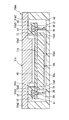
- FIG. 1 is a cross-sectional view illustrating a schematic configuration of an electronic structure according to an embodiment.
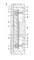
- FIG. 2 is a plan view illustrating a schematic configuration of the electronic device according to the embodiment.
- 3 is a cross-sectional view taken along line III-III in FIG.
- FIG. 4 is a perspective view showing a schematic configuration of the cap in the embodiment.
- FIG. 5 is a cross-sectional view illustrating a manufacturing process of the electronic device according to the embodiment.
- FIG. 6 is a cross-sectional view showing a schematic configuration of the electronic structure in Modification 1.
- FIG. 1 is a cross-sectional view illustrating a schematic configuration of an electronic structure according to an embodiment.
- FIG. 2 is a plan view illustrating a schematic configuration of the electronic device according to the embodiment.
- 3 is a cross-sectional view taken along line III-III in FIG.
- FIG. 4 is a perspective view showing a schematic configuration of the cap in the embodiment.
- FIG. 5 is a cross-sectional
- FIG. 7 is a cross-sectional view showing a schematic configuration of the electronic structure in Modification 2.
- FIG. 8 is a plan view showing a schematic configuration of a cap in Modification 3.
- FIG. 9 is a sectional view taken along line IX-IX in FIG.
- FIG. 10 is a plan view showing a schematic configuration of a cap in Modification Example 4
- FIG. 11 is a cross-sectional view taken along line XI-XI in FIG.
- FIG. 12 is a plan view showing a schematic configuration of a base material in Modification Example 5
- FIG. 13 is a plan view showing a schematic configuration of the base substrate in Modification 6.
- FIG. 14 is a bottom view showing a schematic configuration of an electronic device according to Modification 6.
- FIG. 14 is a bottom view showing a schematic configuration of an electronic device according to Modification 6.
- FIG. 15 is a top view illustrating a schematic configuration of an electronic device according to Modification Example 6, 16 is a cross-sectional view taken along line XVI-XVI in FIG.
- FIG. 17 is a cross-sectional view showing a schematic configuration of the electronic structure in Modification Example 7, and
- FIG. 18 is a cross-sectional view showing a schematic configuration of an electronic structure in Modification 8.
- the electronic structure 100 includes an electronic device 10, a terminal 20, and a first member 31 and a second member 32 that form an accommodation space for accommodating the electronic device 10. Configured.
- the electronic device 10 includes a base material 11, a mold resin 12, a cap 13, an electronic component 14, and the like. The electronic device 10 will be described in detail later.
- the terminal 20 is a part of a connector of an external device provided outside the electronic device 10.
- the terminal 20 employs a press-fit terminal provided with a deformed portion 21.
- the terminal 20 employs a so-called press-fit terminal.
- the deformed portion 21 is deformed by inserting the terminal 20 into a through hole TH provided in the electronic device 10 described later.
- the deformed portion 21 is a portion that stays in the through hole TH when the terminal 20 is inserted into the through hole TH.
- transformation part 21 has a ring shape.
- the terminal 20 is configured such that the deformation portion 21 is deformed when inserted into the through hole TH. That is, when the deformed portion 21 is inserted into the through hole TH, the deformed portion 21 receives stress from the conductive member 18 provided on the surface of the through hole TH. Therefore, it can be said that the terminal 20 is press-fitted into the through hole TH. Further, it can be said that the terminal 20 is in contact with the conductive member 18 by the reaction force of the deformable portion 21.
- the terminal 20 is press-fitted into the through hole TH and is electrically connected to the electronic device 10.
- the terminal 20 is provided on a second member 32 which will be described later. More specifically, in the terminal 20, a portion disposed in the accommodation space s2, such as the deforming portion 21, a portion embedded in the second member 32, and a portion disposed outside the accommodation space s2 are integrated. Is formed. However, here, illustration of a portion embedded in the second member 32 and a portion disposed outside the accommodation space s2 is omitted.
- the first member 31 and the second member 32 correspond to housing members. That is, the first member 31 and the second member 32 are cases that house the electronic device 10.
- the first member 31 is a lid that closes the opening of the box-shaped second member 32, and is joined to the second member 32 to form an accommodation space s ⁇ b> 2 of the electronic device 10. Yes.
- the first member 31 includes a portion facing the surface of the base 11 of the electronic device 10 where the cap 13 is mounted, and is mechanically connected to the electronic device 10 via an adhesive 40.
- an example is employed in which the first member 31 and the mold resin 12 of the electronic device 10 are mechanically connected via the adhesive 40.
- the first member 31 is made of metal and has a function as a heat radiating member. That is, the first member 31 dissipates heat generated from the electronic device 10 from the mold resin 12 side. More specifically, the first member 31 radiates heat generated by the operation of the electronic component 14 provided in the electronic device 10. For this reason, the 1st member 31 can employ
- the adhesive 40 employs a heat dissipating adhesive to transmit heat generated from the electronic device 10 to the first member 31. That is, the adhesive 40 has a function for mechanically connecting the mold resin 12 and the first member 31 and a function for transferring the heat generated from the electronic device 10 to the first member 31. Yes.
- the adhesive 40 corresponds to a member having heat dissipation properties.
- the first member 31 and the electronic device 10 are mechanically connected via the adhesive 40 .
- the present disclosure is not limited to this.
- the first member 31 and the electronic device 10 may be in contact with, for example, heat radiation grease mainly containing silicone. That is, the first member 31 and the electronic device 10 may be in contact with each other via a member having a function for transmitting heat generated from the electronic device 10 to the first member 31.
- heat radiation grease can be employed instead of the adhesive 40.
- the second member 32 is joined to the first member 31 to form the accommodation space s2, includes a portion facing the surface of the substrate 11 where the cap 13 is not mounted, and the terminal 20 is in the accommodation space s2. Protrusively provided.
- the second member 32 is a box-shaped member having a bottom portion and an annular side wall portion protruding from the bottom portion. In other words, the second member 32 is a box member having one surface opened. The opening of the second member 32 is closed by the first member 31 by joining the first member 31 to the tip of the side wall portion.
- the bottom portion includes a portion facing the surface of the base material 11 where the cap 13 is not mounted.
- the second member 32 is made of, for example, resin, and the terminal 20 is insert-molded.
- the second member 32 is employed in which a part of the terminal 20 is provided so as to protrude from the bottom to the accommodation space s2.
- the electronic device 10 includes a circuit board and a mold resin 12. As shown in FIG. 1 and FIG. 3, the circuit board is electrically connected to the insulating base material 11, wiring 17 formed on the base material 11, and mounted on the base material 11. A circuit board including the electronic component 14 is included.
- the electronic device 10 has a through-hole TH in which a conductive member 18 formed so as to penetrate from the one surface a1 of the base material 11 to the opposite surface a2 of the one surface a1 and electrically connected to the wiring 17 is formed on the surface. Is formed.
- the base material 11 is made of an insulating material such as resin or ceramic.
- the base material 11 has a flat plate shape, for example, and has a surface a1 and a surface a2 opposite to the surface a1.
- the substrate 11 is also formed with a laser via hole or a blind via hole as an interlayer connection member.
- the substrate 11 has at least one through hole TH formed therein.
- the base material 11 in which a plurality of through holes TH are formed is employed. More specifically, in the present embodiment, an example is adopted in which through holes TH are provided in two rows at both ends of the base material 11.
- This through hole TH is a part for electrically connecting the terminal 20 and the wiring 17 and is provided in the same number as the number of terminals 20 of the external device or more than the number of terminals 20 of the external device. .
- Each through hole TH has one opening covered with a cap 13. The cap 13 will be described later.
- the wiring 17 is made of a conductive member, and is formed inside or on the surface of the base material 11.
- the wiring 17 is formed in a foil shape, for example. Further, the wiring 17 includes a land on which the electronic component 14 is mounted as a part thereof.
- the structure in which the wiring 17 and the through hole TH are formed on the base material 11 can also be referred to as a printed board.
- the electronic component 14 is mounted on one surface a1 of the substrate 11 and is electrically connected to the wiring 17 and the like.
- the electronic component 14 is an element sealed with a mold resin 12 described later.
- the electronic component 14 is mounted on the base material 11 via the solder 16.
- the solder 16 corresponds to a conductive connection member. Note that the electronic component 14 may be mounted on the base material 11 via a conductive adhesive different from the solder 16.
- an outer resin element 15 that is not sealed with the mold resin 12 is mounted on the opposite surface a2 of the substrate 11. That is, it can be said that the electronic device 10 includes a double-sided mounting board. However, the present disclosure is not limited to this. The electronic device 10 can be employed even if it includes a single-sided mounting board in which the electronic component 14 is mounted on one side of the base material 11.
- the non-resin element 15 corresponds to a back circuit element.
- Mold resin 12 corresponds to sealing resin.
- the mold resin 12 is made of, for example, an epoxy resin and seals the electronic component 14.
- the mold resin 12 integrally seals a connection portion between the electronic component 14 and the base material 11. Further, the mold resin 12 seals the electronic component 14 and the like while being in close contact with at least a part of the one surface a1 of the substrate 11. In other words, it can be said that the mold resin 12 integrally seals the electronic component 14 and the periphery of the electronic component 14 on the one surface a1.
- the mold resin 12 is mechanically connected to the first member 31 via an adhesive 40 as shown in FIG.
- the adhesive 40 is formed on the surface of the mold resin 12 parallel to the one surface a ⁇ b> 1 of the substrate 11, and the adhesive 40 is mechanically connected to the first member 31.
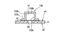
- the cap 13 is mounted on the base material 11, and has an annular connection portion 131 that is a portion connected to the base material 11, and a concave portion 132 that is recessed from the connection portion 131. Is included.
- the concave portion 132 is formed by a ceiling portion 134 and an annular side wall portion 133 that is provided so as to protrude from the ceiling portion 134. That is, the cap 13 is a cylindrical member having a bottom on one side.
- the cap 13 having a shape in which the contents of the column are hollowed out is employed.
- the present disclosure is not limited to this.
- the present disclosure can be used even with the bowl-shaped cap 13 in which the contents of the hemisphere are hollowed out.
- the cap 13 has the connecting portion 131 mechanically connected to the base material 11 with the recess 132 facing the open end of the through hole TH on the one surface a1 side. That is, the cap 13 is mechanically connected to the annular connecting portion 131 around the through hole TH. Further, the cap 13 is connected to the base material 11 in this way, thereby forming a space s1 communicating with the through hole TH. Furthermore, the cap 13 is integrally sealed together with the electronic component 14 by the mold resin 12 as shown in FIGS. Thus, the cap 13 is disposed so as to face one opening end of the target through hole TH, and is not disposed so as to face both opening ends of the target through hole TH. Further, the tip of the terminal 20 is arranged in the space s1. In FIG. 2, the mold resin 12 and the through hole TH are indicated by a two-dot chain line in order to make the drawing easy to see.
- the caps 13 are individually provided corresponding to the plurality of through holes. That is, the electronic device 10 is provided with the same number of caps 13 as the through holes TH, and one cap 13 is provided for one through hole TH. Therefore, it can be said that each cap 13 is provided separately.
- the cap 13 illustrated by the alternate long and short dash line in FIG. 2 is a virtual cap illustrated for explaining the effect of the present disclosure.
- the cap 13 is formed of, for example, metal, resin, ceramics or the like. In the present embodiment, a cap 13 made of metal is employed. Therefore, the cap 13 can be mounted on the base material 11 via the solder 16. Further, as shown in FIGS. 2 and 3, the cap 13 is mounted on one surface a1 on which the electronic component 14 is mounted. That is, the cap 13 and the electronic component 14 are mounted on the same surface of the substrate 11. For this reason, the cap 13 can be mounted together with the electronic component 14 on the base material 11. In other words, the cap 13 can be mounted on the substrate 11 in the same process as the electronic component 14. The cap 13 can be mounted on the base material 11 in the same process as the electronic component 14 as long as at least the connection portion 131 is made of metal.
- the mold resin 12 sealing the cap 13 and the electronic component 14 can be formed by, for example, compression molding or transfer molding.
- compression molding a molding process for compression molding the molding resin 12 will be described with reference to FIG.
- an upper mold 210 and a lower mold including the fixed portion 221 and the movable portion 222 are used as the mold.
- the upper mold 210 is a surface with which the opposite surface a2 of the base material 11 is brought into contact, and has a flat contact surface.
- a fixed portion 221 provided with a hole, and a movable portion 222 that can move along the hole are disposed in the hole.
- a cavity in which a resin material to be the mold resin 12 is disposed is formed by the fixed portion 221 and the movable portion 222.
- the movable part 222 can move up and down in the hole of the fixed part 221.
- the movable part 222 is movable in a direction approaching the upper mold 210 and a direction moving away from the upper mold 210 in a state where the electronic device 10 before molding is fixed to the upper mold 210 and the fixing part 221. Can do.
- the contact surface of the upper mold 210 is brought into contact with the opposite surface a2 of the base material 11, and the fixing portion 221 is brought into contact with the one surface a1 of the electronic device 10.
- the lower mold causes the fixing portion 221 to come into contact with the one surface a1 of the electronic device 10 so that the cavity faces the mounting region where the cap 13 and the electronic component 14 are mounted on the one surface a1 of the base material 11.
- the movable portion 222 is moved toward the upper mold 210 in a state where the resin material is put in the cavity, and a forming pressure is applied to the resin material.
- the mold is heated to a predetermined temperature in order to apply heat to the resin material.
- the molding resin 12 is formed by curing the resin material while applying the forming pressure. In this way, the cap 13 and the electronic component 14 are collectively sealed in the molding process.
- the electronic device 10 since the cap 13 is put on the through hole TH, the resin material can be prevented from entering the through hole TH. Therefore, the electronic device 10 can make the inside of the cap 13 hollow even after the mold resin 12 is provided.
- the electronic device 10 and the first member 31 are mechanically connected via the adhesive 40.
- the mold resin 12 and the first member 31 are mechanically connected by the adhesive 40 in a state where the mold resin 12 and the first member 31 of the electronic device 10 face each other.
- the electronic device 10 and the first member 31 manufactured by the first step are mechanically connected to each other and also referred to as a first structure.
- the first structure is assembled to the second member 32.
- the first member 31 is joined to the tip of the side wall portion of the second member 32 in a state where the electronic device 10 is disposed in the space surrounded by the bottom portion of the second member 32 and the annular side wall portion. .
- the first member 31 is bonded to the tip of the side wall portion of the second member 32, thereby closing the opening of the second member 32.
- the electronic device 10 is placed in a space surrounded by the bottom and the annular side wall while the terminal 20 is press-fitted into the through hole TH. Further, in the second step, in order to press-fit the terminal 20 into the through hole TH, the first structure is pushed from the opening side of the second member 32 to the bottom side with the through hole TH and the terminal 20 aligned. . As described above, the electronic device 10 is disposed in the accommodation space s ⁇ b> 2 while being mechanically connected to the first member 31.
- the electronic structure 100 can also be manufactured by the second manufacturing method in which the first member 31 is joined to the second member 32 after the electronic device 10 is assembled to the second member 32.
- the electronic device 10 in the first step, is arranged in a space surrounded by the bottom of the second member 32 and the annular side wall.
- the electronic device 10 is disposed in a space surrounded by the bottom and the annular side wall while the terminal 20 is press-fitted into the through hole TH.
- the electronic device 10 in order to press-fit the terminal 20 into the through hole TH, the electronic device 10 is pushed from the opening side of the second member 32 to the bottom side with the through hole TH and the terminal 20 aligned. Thereby, the electronic device 10 is electrically connected to the terminal 20 and assembled to the second member 32.
- the electronic device 10 and the second member 32 manufactured by the first process are also referred to as a second structure.
- the first member 31 is assembled to the second structure.
- the first member 31 is joined to the tip of the side wall portion of the second member 32.
- the first member 31 is bonded to the tip of the side wall portion of the second member 32, thereby closing the opening of the second member 32.
- the first member 31 and the electronic device 10 are mechanically connected via the adhesive 40.
- the mold resin 12 and the first member 31 may be brought into contact with each other through heat radiation grease instead of the adhesive 40.
- the terminal 20 is inserted into the through hole TH provided in the base material 11.
- the electronic device 10 includes a cap 13 including an annular connection portion 131 connected to the base material 11 and a recess portion 132 that is recessed from the connection portion 131.
- the cap 13 has the concave portion 132 facing the opening end of the through hole TH, and the connecting portion 131 is connected to the base material 11 to form a space s1 that communicates with the through hole TH. It is sealed together with the component 14. That is, in the electronic device 10, the cap 13 is put on the opening end of the through hole TH, and the cap 13 is sealed with the mold resin 12.
- the electronic device 10 even when the tip of the terminal 20 inserted into the through hole TH is exposed from the through hole TH, the tip is covered with the cap 13 and the mold resin 12. That is, even when the tip of the terminal 20 is exposed from the through hole TH, the electronic device 10 is only disposed in the space s1 communicating with the through hole TH and is not exposed to the outside of the mold resin 12. Therefore, when the terminal 20 is inserted into the through hole TH, the electronic device 10 can ensure insulation between the terminal 20 and the different potential member. That is, the electronic device 10 does not need to perform a special process for preventing a short circuit between the terminal 20 and the first member 31.
- the electronic device 10 has a cap 13 covering the through hole TH. For this reason, the electronic device 10 can suppress the mold resin 12 from entering the through hole TH when the mold resin 12 is provided. For this reason, the electronic device 10 can suppress a decrease in electrical connectivity between the conductive member 18 and the terminal 20.
- the electronic device 10 suppresses the mold resin 12 from entering the through hole TH by the cap 13 as described above. For this reason, the electronic device 10 needs only to change the position of the cap 13 according to the position of the through hole TH when the mold resin 12 is provided on the base material 11 having a different position of the through hole TH, and it is necessary to process the mold. There is no.
- the electronic device 10 is illustrated with a cap 13 illustrated by a one-dot chain line, and an electronic device in which a through hole TH is provided at a position facing the cap 13 (hereinafter referred to as a modified electronic device).
- a modified electronic device an electronic device in which a through hole TH is provided at a position facing the cap 13
- a cap 13 is provided.
- the electronic device 10 and the modified electronic device are different in the positions of the through holes TH, since the caps 13 are put on all the through holes TH, the cap 13 prevents the mold resin 12 from entering the through holes TH. Yes. Therefore, although the electronic device 10 and the modified electronic device are different in the position of the through hole TH, they can be manufactured with the same mold if the position of the cap 13 is changed in accordance with the position of the through hole TH. Thus, the electronic device 10 can improve the degree of freedom of the position of the through hole TH.
- the electronic device 10 since the electronic device 10 is covered with the cap 13 on the opening end of the through hole TH and the cap 13 is sealed with the mold resin 12, the strength around the through hole TH can be improved. Therefore, the electronic device 10 can suppress the base material 11 from being distorted by the stress from the terminal 20 when the terminal 20 is press-fitted into the through hole TH. That is, the electronic device 10 can suppress the distortion of the base material 11 without reinforcing the periphery of the through hole TH with a jig. Moreover, since the electronic device 10 can suppress the distortion of the base material 11, it is possible to suppress the wiring 17 from being disconnected due to the distortion of the base material 11.
- the first member 31 and the second member 32 form an accommodation space s2, and the electronic device 10 is accommodated in the accommodation space s2. Therefore, the electronic structure 100 can suppress foreign matter from adhering to the electronic device 10.
- the first member 31 made of metal is mechanically connected to the electronic device 10. Therefore, the electronic structure 100 can dissipate heat through the first member 31 even when heat is generated from the electronic device 10. Note that the electronic structure 100 can dissipate heat generated from the electronic device 10 even when the electronic device 10 and the first member 31 are in contact with each other via heat dissipation grease.
- the electronic device 10 can ensure the insulation between the terminal 20 and the different potential member as described above. Therefore, in the electronic structure 100, even if the first member 31 is made of metal and includes a portion facing the surface on which the cap 13 is mounted on the base material 11, the insulation between the terminal 20 and the first member 31 is included. Can be secured.
- Modification 1 As shown in FIG. 6, the electronic device 10 a of Modification 1 has a cap 13 mounted on the back surface of the base 11 a on which the electronic component 14 is mounted.
- an electronic device 10a in which the electronic component 14 is mounted on one surface a1 of the substrate 11a and the cap 13 is mounted on the opposite surface a2 of the substrate 11a is employed.
- the base material 11a is provided with a through hole 11a1 in order to mold each part of the mold resin at once.
- the element sealing portion 12a1 and the cap sealing portion 12a3 are molded by the resin material serving as the mold resin passing through the through hole 11a1.
- the connecting portion 12a2 is provided in the through hole 11a1.
- the mold used for molding the electronic device 10a is provided with a space for forming the element sealing portion 12a1 and a space for forming the cap sealing portion 12a3, both of which are through holes 11a1. It is communicated by.
- the electronic device 10a can achieve the same effects as the electronic device 10.
- the electronic structure 100a of Modification 1 includes a terminal 20, a first member 31a, and a second member 32a in addition to the electronic device 10a.
- the second member 32a is the same as the second member 32, and a description thereof will be omitted.
- the first member 31a is a part mechanically connected to the electronic device 10a, and is provided with a protruding part 31a1 protruding from the periphery. That is, the first member 31a includes a protruding portion 31a1 and a peripheral portion 31a2 that is recessed from the protruding portion 31a1 provided in the periphery of the protruding portion 31a1. In other words, the first member 31a has a step formed by the protruding portion 31a1 and the peripheral portion 31a2 on the side facing the electronic device 10a, and the protruding portion 31a1 protrudes from the peripheral portion 31a2. Moreover, the thickness of the protrusion part 31a1 is formed thinner than the thickness of the cap sealing part 12a3. The difference between the thickness of the protruding portion 31a1 and the thickness of the cap sealing portion 12a3 is the thickness of the adhesive 40.
- the thickness of the protrusion 31a1 corresponds to the distance between the virtual plane along the surface on the accommodation space s2 side in the peripheral portion 31a2 and the virtual plane along the surface on the accommodation space s2 side in the protrusion 31a1.
- the thickness of the cap sealing part 12a3 is the thickness of the thickest part in the cap sealing part 12a3, a virtual plane along the surface of the cap sealing part 12a3 opposite to the base material 11a, and the base material This corresponds to the distance from the opposite surface a2 of 11a.
- the thickness of the cap sealing portion 12a3 corresponds to a length obtained by adding the thickness of the portion provided on the cap 13 in the cap sealing portion 12a3 to the height of the cap 13.
- the protrusion 31a1 is mechanically connected to a part of the opposite surface a2 via the adhesive 40. That is, in the electronic device 10a, the protruding portion 31a1 is connected to the periphery of the cap sealing portion 12a3 on the opposite surface a2. Further, in the electronic structure 100a, the cap sealing portion 12a3 is in contact with the peripheral portion 31a2 in a state where the protruding portion 31a1 is mechanically connected to the electronic device 10a. Therefore, it can be said that the thickness of the cap sealing portion 12a3 is a thickness obtained by adding the thickness of the protruding portion 31a1 and the thickness of the adhesive 40.
- the electronic structure 100a can achieve the same effects as the electronic structure 100. Furthermore, when the electronic structure 100a mechanically connects the first member 31a and the electronic device 10a, the peripheral portion 31a2 and the cap sealing portion 12a3 are in contact with each other. Easy to manage the thickness. That is, the electronic structure 100a can manage the thickness of the adhesive 40 by manufacturing the cap sealing portion 12a3 and the protruding portion 31a1 so as to have a thickness corresponding to the desired thickness of the adhesive 40. it can. In other words, the electronic structure 100a can easily manage the thickness of the adhesive by controlling the thickness of the cap sealing portion 12a3 and the thickness of the protruding portion 31a1. Accordingly, the electronic structure 100a can easily manage the contact area between the first member 31a and the electronic device 10a. Therefore, the electronic structure 100a can efficiently radiate heat from the electronic device 10a.
- the heat dissipating member 60 is mechanically connected to the opposite surface a2 of the base material 11 via an adhesive 50.
- the resin outer element 15 is not mounted on the opposite surface a2. That is, the electronic device 10b includes a circuit board that is a single-sided mounting board.
- the electronic device 10b has a circuit board that is a single-sided mounting board, and is disposed in the accommodation space s2 formed by the first member 31b and the second member 32b.
- the first member 31b is mechanically connected to the one surface a1 side
- the heat dissipation member 60 is mechanically connected to the opposite surface a2 side. Since the adhesive 50 is the same as the adhesive 40, the description thereof is omitted.
- the electronic structure 100b can achieve the same effects as the electronic structure 100. Furthermore, the electronic structure 100b can dissipate the electronic device 10b from both sides of the one surface a1 side and the opposite surface a2 side. Therefore, the electronic structure 100b can improve the heat dissipation of the electronic device 10b more than the electronic structure 100.
- the non-resin element 15 may be mounted around the adhesive 50 in the base material 11. Further, the heat dissipating member 60 and the electronic device 10b may be in contact with each other through heat dissipating grease instead of the adhesive 50.
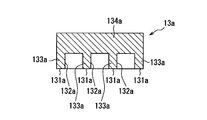
- Modification 3 The electronic device of Modification 3 is provided with a cap 13a as shown in FIGS. In other words, the electronic device of Modification 3 is different from the electronic device 10 in the configuration of the cap 13a.
- the cap 13 a is an integrated object provided with a plurality of recesses 132 a partitioned from each other.
- the substrate 11 has a plurality of through holes TH. Therefore, the cap 13a is provided with a recess 132a corresponding to at least two through holes TH among the plurality of through holes TH.
- each recess 132a is formed by a ceiling part 134a and an annular side wall part 133a provided so as to protrude from the ceiling part 134a. That is, each recessed part 132a is partitioned off by the side wall part 133a.
- each recessed part 132a is a site
- the cap 13a provided with three concave portions 132a corresponding to the three through holes TH is employed.
- the electronic device of Modification 3 can achieve the same effects as the electronic device 10. Furthermore, since the electronic device of Modification 3 employs the cap 13a provided with a plurality of recesses 132a, the same number of through holes TH as the number of the recesses 132a can be collectively covered.
- both the cap 13 and the cap 13 a may be mounted on the base material 11.
- the cap 13 a is mounted in a region where the through holes TH are dense in the base material 11, and the cap 13 is mounted in a region where the through hole TH is provided alone. Also good.
- the cap 13 a is mounted in a region where the plurality of through holes TH are provided adjacent to each other without the electronic component 14 interposed therebetween, and the through hole is provided between the electronic component 14.
- the cap 13 may be mounted in a region where the head is located.
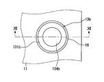
- Modification 4 The electronic device of Modification 4 is provided with a cap 13b as shown in FIGS. That is, the electronic device of Modification 4 is different from the electronic device 10 in the configuration of the cap 13b.
- the cap 13b includes a recess 132b and a flange 131b as a connecting portion protruding from the recess 132b.
- the recessed part 132b is formed of the ceiling part 134b and the cyclic
- the flange 131b is provided so as to protrude from the end of the side wall 133b to the outside of the recess 132b along the plane of the base material 11. As shown in FIG. 10, the flange 131b is provided over the entire circumference of the side wall 133b.
- the flange 131b is provided so as to expand outward, that is, on the side opposite to the recess 132b with respect to the side wall portion 133b.
- the plane of the base material 11 is a mounting surface on which the cap 13b of the base material 11 is mounted, and here is the one surface a1.
- the electronic device of Modification 4 can achieve the same effects as the electronic device 10. Furthermore, since the electronic device of the modification 4 employs the cap 13b having the flange 131b, the cap 13b and the base material 11 can be mechanically connected more firmly. Therefore, the electronic device of Modification 4 can further improve the leakage of the mold resin 12 into the through hole TH. For this reason, the electronic device of the modification 4 can suppress further the fall of the electrical connectivity of the electroconductive member 18 and the terminal 20 further.
- the flange 131b may be provided in a part of the entire periphery of the end portion of the side wall portion 133b as long as the front end surface of the side wall portion 133b is provided in an annular shape.
- Modification 5 As shown in FIG. 12, in the electronic device according to the fifth modification, a plurality of lands 19 are provided in the opposing region of the connection portion 131 in the base material 11 at intervals. As described above, the electronic device of Modification 5 is different in the configuration of the electronic device 10 of the above embodiment and the base material 11 in that the land 19 is provided. However, here, for convenience, description will be made using the same reference numerals.
- the cap 13 is mounted on the base material 11 via a plurality of lands 19. Therefore, the cap 13 is partially mechanically connected to the base material 11.
- the connection portion 131 of the cap 13 includes a portion that is connected to the base material 11 and includes a portion that is not connected to the base material 11.
- a gap is partially formed between the base material 11 and the connection portion 131.
- the electronic device of Modification 5 is provided with a plurality of lands 19 at intervals so as to function as an air vent when the mold resin 12 is molded.
- the plurality of lands 19 are provided at intervals such that the resin material that becomes the mold resin 12 does not leak out while allowing air to pass during molding.
- the land 19 is normally formed thin enough so that the resin material that becomes the mold resin 12 does not leak through the air during molding.
- the electronic device according to the modified example 5 when the mold resin 12 is molded, the resin material that becomes the mold resin 12 leaks from the gap between the base material 11 and the connection portion 131, that is, between the plurality of lands 19. While suppressing this, air in the mold cavity can be released. That is, the electronic device of Modification 5 can release air from between the plurality of lands 19 to the through hole TH during molding.
- the electronic device of Modification 5 can achieve the same effects as the electronic device 10. Furthermore, since the electronic device of Modification 5 can release air during molding, it can suppress the formation of bubbles in the mold resin 12. That is, the electronic device of Modification 5 includes the mold resin 12 that has no bubbles or few bubbles.
- the cap 13 a and the cap 13 b may be mounted on the base material 11 via the plurality of lands 19.
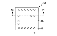
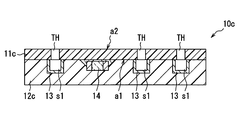
- Modification 6 As shown in FIGS. 14 to 16, in the electronic device 10c of Modification 6, the entire surface of the substrate 11c on which the electronic component 14 is mounted is covered with the mold resin 12c. That is, the entire surface a1 of the base material 11c is covered with the mold resin 12c.
- the electronic device 10c can only see the mold resin 12c when viewed from the mold resin 12c side. Further, as shown in FIG. 15, when the electronic device 10 c is viewed from the base material 11 c side, the cap 13 can be seen through the base material 11 c, the through hole TH, and the through hole TH. In the electronic device 10c, as shown in FIG. 16, the side surface of the base material 11c and the side surface of the mold resin 12c are flush with each other. The electronic device 10c can achieve the same effects as the electronic device 10.
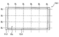
- the electronic device 10c can be manufactured by dicing the base substrate 10c1 with a dicing line DL as shown in FIG.
- the base substrate 10c1 has a plurality of regions to be a plurality of electronic devices 10c. That is, in the base substrate 10c1, the cap 13 and the electronic component 14 are mounted on the base material 11c1 before being divided into the plurality of base materials 11c, and the mold resin 12c1 before the cap 13 and the electronic component 14 are divided. It is sealed with.
- the base substrate 10c1 of FIG. 13 has 15 electronic devices 10c integrally formed. Therefore, the base substrate 10c1 is divided into 15 electronic devices 10c when diced along the dicing line DL.
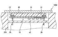
- the electronic structure 100 c of Modification 7 is provided with a terminal 20 a that is not a press-fit terminal such as the terminal 20.
- the electronic structure 100c includes a terminal 20a, a first member 31c similar to the first member 31, and a lid portion 32c and a side wall portion 33 as second members.
- illustration of the resin outer element 15, the wiring 17, the conductive member 18, and the like in the electronic device 10 is omitted.
- the electronic device 10 refer to the above embodiment.
- the terminal 20a is inserted into the through hole TH and is electrically connected to the conductive member 18 by the solder 70. That is, the terminal 20a is electrically connected to the conductive member 18 without directly contacting the through hole TH.
- the electronic structure 100c includes a lid portion 32c and a side wall portion 33 which are separate members as a second member in order to easily connect the terminal 20a and the conductive member 18 with the solder 70. That is, in the electronic structure 100c, it can be said that the bottom portion and the side wall portion of the second member 32 are provided separately. Therefore, the lid portion 32 c corresponds to the bottom portion of the second member 32, and the side wall portion 33 corresponds to the side wall portion of the second member 32. Further, the side wall 33 has one opening closed by the first member 31c and the other opening closed by the lid 32c. Note that the electronic device is mechanically connected to the first member 31c via the adhesive 40 as in the above embodiment.
- the lid portion 32c can employ, for example, a plate-like member in the same manner as the first member 31c.
- the side wall part 33 is a cylindrical member, for example, and the terminal 20a is insert-molded.
- the terminal 20a has a portion bent in an L shape disposed in the accommodation space s2.
- the electronic structure 100c can be manufactured by the following processes, for example. First, in the first step, the electronic device 10 is mechanically connected to the first member 31c via the adhesive 40. In the next step, the side wall portion 33 is inserted into the through hole TH while the terminal 20a provided on the side wall portion 33 is inserted into the state in which the first member 31c and the electronic device 10 are mechanically connected. And the first member 31c are joined. As a result, one opening of the side wall 33 is closed by the first member 31c.
- the conductive member 18 and the terminal 20 a inserted into the through hole TH are electrically connected by the solder 70.
- the lid portion 32 c is joined to the side wall portion 33.
- the other opening of the side wall 33 is closed by the lid 32c. That is, both openings of the side wall portion 33 are closed by the first member 31c and the lid portion 32c. Therefore, the electronic device is accommodated in the accommodation space s2 formed by the first member 31c, the lid portion 32c, and the side wall portion 33.
- the electronic device 10 can achieve the object of the present disclosure even if such a terminal 20a is inserted into the through hole TH.
- the electronic structure 100c can achieve the same effects as the electronic structure 100.
- the terminal 20 a may be electrically connected to the conductive member 18 with a conductive adhesive different from the solder 70. That is, the terminal 20a only needs to be electrically connected to the conductive member 18 by the conductive connection member.
- the second member 32d may be a part of an external device. That is, the terminal 20 may be provided in an external device.
- the electronic device 10 is integrally assembled with an external device.
- the electronic structure 100d can achieve the same effects as the electronic structure 100.
Landscapes
- Engineering & Computer Science (AREA)
- Microelectronics & Electronic Packaging (AREA)
- Power Engineering (AREA)
- Physics & Mathematics (AREA)
- Condensed Matter Physics & Semiconductors (AREA)
- General Physics & Mathematics (AREA)
- Computer Hardware Design (AREA)
- Manufacturing & Machinery (AREA)
- Geometry (AREA)
- Structures Or Materials For Encapsulating Or Coating Semiconductor Devices Or Solid State Devices (AREA)
- Casings For Electric Apparatus (AREA)
- Materials Engineering (AREA)
- Chemical & Material Sciences (AREA)
- Non-Metallic Protective Coatings For Printed Circuits (AREA)
Abstract
電子装置は、絶縁性の基材(11,11a,11c)と、前記基材に形成された配線(17)と、前記配線に電気的に接続された電子部品(14)と、前記基材の一面から反対面に亘って貫通して形成され、表面に前記配線と電気的に接続された導電性部材(18)が形成された少なくとも一つのスルーホール(TH)とを含む回路基板を備えており、封止樹脂(12,12a1~12a3,12c)と、前記基材と接続される部位を含む環状の接続部(131,131a,131b)と、環状の前記接続部から凹んだ凹部(132,132a,132b)とを含むキャップ(13,13a,13b)と、をさらに備える。前記キャップは、前記接続部の少なくとも一部が前記基材に接続されて、前記スルーホールと連通した空間を形成しつつ、前記封止樹脂によって前記電子部品と共に一体的に封止されており、端子(20,20a)が前記スルーホールに挿入されて前記配線と電気的に接続されてなる。
Description
本出願は、2014年9月22日に出願された日本出願番号2014-192745号に基づくもので、ここにその記載内容を援用する。
本開示は、端子が挿入されるスルーホールが設けられた回路基板を含む電子装置、及び電子装置を備えた電子構造体に関する。
従来、特許文献1に開示されているように、回路基板に設けられたスルーホールに端子が挿入される技術がある。
ところで、従来技術ではないが、上記回路基板に電子部品が実装されており、その電子部品が封止樹脂で封止されている電子装置が考えられる。また、このような電子装置では、端子の先端がスルーホールから露出した場合、意図せずに、端子と周辺の部材とが電気的に接続されることが起こりうる。電子装置では、端子と周辺の部材とを電気的に絶縁するために、スルーホールに対向する領域に達するように封止樹脂を形成することが考えられる。なお、ここでの周辺の部材とは、端子とは電位が異なる異電位部材である。
しかしながら、電子装置は、スルーホールに封止樹脂に入り込まないようにする必要がある。スルーホールに封止樹脂が入り込まないようにするためには、例えば、スルーホールに対応した突起が形成された金型を用いて封止樹脂を形成することが考えられる。つまり、この製造方法では、金型の突起をスルーホールに挿入してスルーホールを塞いだ状態で封止樹脂を形成する。
ところが、上記製造方法で製造された電子装置は、金型における突起の位置にスルーホールの位置が限定されてしまう。また、スルーホール位置を変更するためには、金型を加工して、突起の位置を変更する必要がある。よって、このような電子装置は、スルーホール位置の自由度が低くなってしまう。
本開示は、スルーホールに挿入される端子の絶縁性を確保しつつ、スルーホール位置の自由度を向上させることができる電子装置及び電子装置を備えた電子構造体を提供する。
本開示の第一態様に係る電子装置は、絶縁性の基材と、前記基材に形成された配線と、前記基材に実装されて前記配線に電気的に接続された電子部品と、前記基材の一面から前記基材の一面の反対面に亘って貫通して形成され、表面に前記配線と電気的に接続された導電性部材が形成された少なくとも一つのスルーホールとを含む回路基板を備えており、前記電子部品を封止している封止樹脂と、前記基材に実装されるものであり、前記基材と接続される部位を含む環状の接続部と、環状の前記接続部から凹んだ凹部とを含むキャップと、をさらに備える。前記キャップは、前記凹部が前記スルーホールにおける前記基材の一面の開口端及び前記基材の一面の反対面の開口端の一方に対向した状態で、前記接続部の少なくとも一部が前記基材に接続されて、前記スルーホールと連通した空間を形成しつつ、前記封止樹脂によって前記電子部品と共に一体的に封止されており、端子が前記スルーホールに挿入されて前記配線と電気的に接続されてなる。
このため、電子装置は、スルーホールに挿入された端子の先端がスルーホールから露出した場合であっても、その先端がキャップと封止樹脂で覆われることになる。つまり、電子装置は、端子の先端がスルーホールから露出した場合であっても、スルーホールと連通した空間に配置されるだけであり、封止樹脂の外部に露出しない。よって、電子装置は、スルーホールに端子が挿入された際に、その端子と異電位部材との絶縁性を確保できる。
更に、電子装置は、スルーホールにキャップが被せられている。このため、電子装置は、封止樹脂を設ける際に、スルーホールに封止樹脂が入り込むことを抑制できる。電子装置は、このようにキャップによってスルーホールに封止樹脂が入り込むことを抑制しているため、スルーホールの位置が異なる基材に封止樹脂を設ける場合に、スルーホールの位置に合わせてキャップの位置をかえればよい。よって、電子装置は、スルーホールの位置が異なる基材に封止樹脂を設ける場合に、金型を加工する必要がない。よって、電子装置は、スルーホール位置の自由度を向上させることができる。
本開示の第二態様に係る電子構造体は、上記のような電子装置、前記端子と、前記電子装置を収容するための収容空間を形成し、前記収容空間に前記電子装置を収容している収容部材と、を備える。また、前記収容部材は、金属からなり、前記基材における前記キャップが実装されている面と対向する部位を含み、前記電子装置と接している第1部材と、前記第1部材と接合されて前記収容空間を形成するものであり、前記基材における前記キャップが実装されていない面に対向する部位を含み、前記端子が前記収容空間に突出して設けられた第2部材と、を含む。
このように、電子構造体は、第1部材と第2部材とで収容空間を形成し、この収容空間に電子装置を収容している。よって、電子構造体は、電子装置に異物が付着することを抑制できる。また、電子構造体は、金属からなる第1部材が電子装置と接している。よって、電子構造体は、電子装置から熱が発せられた場合であっても、第1部材を介して放熱することができる。また、電子装置は、上記のように端子と異電位部材との絶縁性を確保できる。よって、電子構造体は、第1部材が金属からなり、基材におけるキャップが実装されている面と対向する部位を含んでいても、端子と第1部材との絶縁性を確保できる。
本開示についての上記目的およびその他の目的、特徴や利点は、添付の図面を参照しながら下記の詳細な記述により、より明確になる。その図面は、
図1は、実施形態における電子構造体の概略構成を示す断面図であり、
図2は、実施形態における電子装置の概略構成を示す平面図であり、
図3は、図2のIII-III線に沿う断面図であり、
図4は、実施形態におけるキャップの概略構成を示す斜視図であり、
図5は、実施形態における電子装置の製造工程を示す断面図であり、
図6は、変形例1における電子構造体の概略構成を示す断面図であり、
図7は、変形例2における電子構造体の概略構成を示す断面図であり、
図8は、変形例3におけるキャップの概略構成を示す平面図であり、
図9は、図8のIX-IX線に沿う断面図であり、
図10は、変形例4におけるキャップの概略構成を示す平面図であり、
図11は、図10のXI-XI線に沿う断面図であり、
図12は、変形例5における基材の概略構成を示す平面図であり、
図13は、変形例6におけるベース基板の概略構成を示す平面図であり、
図14は、変形例6における電子装置の概略構成を示す下面図であり、
図15は、変形例6における電子装置の概略構成を示す上面図であり、
図16は、図15のXVI-XVI線に沿う断面図であり、
図17は、変形例7における電子構造体の概略構成を示す断面図であり、及び、
図18は、変形例8における電子構造体の概略構成を示す断面図である。
以下において、図面を参照しながら、発明を実施するための複数の形態を説明する。各形態において、先行する形態で説明した事項に対応する部分には同一の参照符号を付して重複する説明を省略する場合がある。各形態において、構成の一部のみを説明している場合は、構成の他の部分については先行して説明した他の形態を参照し適用することができる。
図1に示すように、電子構造体100は、電子装置10と、端子20と、電子装置10を収容するための収容空間を形成している第1部材31及び第2部材32と、を備えて構成されている。電子装置10は、基材11、モールド樹脂12、キャップ13、電子部品14などを備えて構成されている。なお、電子装置10に関しては、後程詳しく説明する。
まず、端子20、及び第1部材31と第2部材32に関して説明する。端子20は、電子装置10の外部に設けられた外部機器のコネクタの一部である。端子20は、一例として、変形部21が設けられた圧入端子を採用している。言い換えると、端子20は、所謂プレスフィット端子を採用している。端子20は、後程説明する電子装置10に設けられたスルーホールTHに挿入されることで変形部21が変形する。
変形部21は、端子20がスルーホールTHに挿入された際に、スルーホールTH内に留まる部位である。例えば、図1に示すように、変形部21は、輪っか形状を有している。端子20は、スルーホールTHに挿入されると、変形部21が変形するように構成されている。つまり、変形部21は、スルーホールTHに挿入されると、スルーホールTHの表面に設けられている導電性部材18から応力を受けることになる。よって、端子20は、スルーホールTHに圧入されている、と言うことができる。また、端子20は、変形部21の反力によって導電性部材18と接触している、と言うことができる。端子20は、スルーホールTHに圧入されて、電子装置10と電気的に接続されている。
また、端子20は、後程説明する第2部材32に設けられている。詳述すると、端子20は、変形部21など収容空間s2に配置されている部分と、第2部材32に埋設されている部分と、収容空間s2の外部に配置されている部分とが一体的に形成されている。しかしながら、ここでは、第2部材32に埋設されている部分と、収容空間s2の外部に配置されている部分の図示を省略している。
第1部材31と第2部材32とは、収容部材に相当する。つまり、第1部材31と第2部材32とは、電子装置10を収容するケースである。
第1部材31は、図1に示すように、箱状の第2部材32の開口を塞ぐ蓋であり、第2部材32と接合されることで、電子装置10の収容空間s2を形成している。また、第1部材31は、電子装置10の基材11におけるキャップ13が実装されている面と対向する部位を含み、電子装置10と接着剤40を介して機械的に接続されている。本実施形態では、第1部材31と電子装置10のモールド樹脂12とが接着剤40を介して機械的に接続されている例を採用している。
更に、第1部材31は、金属によって形成されており、放熱部材としての機能も有している。つまり、第1部材31は、電子装置10から発せられた熱をモールド樹脂12側から放熱するものである。詳述すると、第1部材31は、電子装置10に設けられている電子部品14が動作することによって発した熱を放熱するものである。このため、第1部材31は、金属プレートを採用できる。接着剤40は、電子装置10から発せられた熱を第1部材31に伝達するために放熱性接着剤を採用している。つまり、接着剤40は、モールド樹脂12と第1部材31とを機械的に接続するための機能と、電子装置10から発せられた熱を第1部材31に伝達するための機能とを備えている。接着剤40は、放熱性を有する部材に相当する。
上記のように、本実施形態では、第1部材31と電子装置10とが接着剤40を介して機械的に接続されている例を採用している。しかしながら、本開示はこれに限定されない。本開示は、第1部材31と電子装置10とが例えばシリコーンを主成分とする放熱グリスなどで接していてもよい。つまり、第1部材31と電子装置10とは、電子装置10から発せられた熱を第1部材31に伝達するための機能を備えている部材を介して接していればよい。なお、後程説明する変形例においても、接着剤40のかわりに放熱グリスを採用できる。
第2部材32は、第1部材31と接合されて収容空間s2を形成するものであり、基材11におけるキャップ13が実装されていない面に対向する部位を含み、端子20が収容空間s2に突出して設けられている。第2部材32は、底部と、底部から突出して設けられた環状の側壁部とを有した箱状の部材である。言い換えると、第2部材32は、一面が開口した箱部材である。そして、第2部材32は、側壁部の先端に第1部材31が接合されることで、第1部材31によって開口が塞がれている。なお、底部は、基材11におけるキャップ13が実装されていない面に対向する部位を含むものである。
また、第2部材32は、例えば、樹脂によって形成されており、端子20がインサート成形されている。本実施形態では、端子20の一部が底部から収容空間s2に突出して設けられている第2部材32を採用している。
ここで、電子装置10に関して説明する。図1などに示すように、電子装置10は、回路基板とモールド樹脂12とを備えて構成されている。回路基板は、図1や図3などに示すように、絶縁性の基材11と、基材11に形成された配線17と、基材11に実装されて配線17に電気的に接続された電子部品14とを含む回路基板などを含むものである。また、電子装置10は、基材11の一面a1から一面a1の反対面a2に亘って貫通して形成され表面に配線17と電気的に接続された導電性部材18が形成されたスルーホールTHが形成されている。
基材11は、樹脂やセラミックなどの絶縁性の材料によって構成されている。基材11は、例えば平板形状を有しており、一面a1と、一面a1の反対面a2とを有している。基材11は、例えば、コア層と複数のビルドアップ層とが積層された所謂ビルドアップ基板や、複数のビルドアップ層が積層された所謂エニーレイヤー基板などを採用できる。詳しい説明は省略するが、基材11には、層間接続部材としてのレーザービアホールやブラインドビアホールなども形成されている。
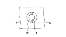
基材11は、少なくとも一つのスルーホールTHが形成されている。本実施形態では、図2に示すように、複数のスルーホールTHが形成された基材11を採用している。詳述すると、本実施形態では、基材11の両端の夫々に、二列ずつスルーホールTHが設けられている例を採用している。このスルーホールTHは、端子20と配線17とを電気的に接続するための部位であり、外部機器の端子20の数と同数、もしくは、外部機器の端子20の数よりも多く設けられている。各スルーホールTHは、一方の開口がキャップ13で覆われている。このキャップ13に関しては、後程説明する。
配線17は、導電性の部材によって構成されており、基材11の内部や表面に形成されている。配線17は、例えば箔状に形成されている。また、配線17は、自身の一部として、電子部品14が実装されるランドなどを含んでいる。なお、基材11に配線17及びスルーホールTHが形成された構造体は、プリント基板と称することもできる。
電子部品14は、基材11の一面a1に実装されて、配線17などと電気的に接続されている。本実施形態では、図2に示すように、複数の電子部品14が実装されている例を採用している。電子部品14は、後程説明するモールド樹脂12で封止される素子である。電子部品14は、例えばMOSFETやチップコンデンサなどを採用できる。また、電子部品14は、半田16を介して基材11に実装されている。この半田16は、導電性接続部材に相当する。なお、電子部品14は、半田16とは異なる導電性接着剤を介して基材11に実装されていてもよい。
また、基材11の反対面a2には、モールド樹脂12で封止されていない樹脂外素子15が実装されている。つまり、電子装置10は、両面実装基板を備えている、と言うことができる。しかしながら、本開示はこれに限定されない。電子装置10は、基材11の片面に電子部品14が実装された片面実装基板を備えているものであっても採用できる。なお、樹脂外素子15は、裏面回路素子に相当する。
モールド樹脂12は、封止樹脂に相当する。モールド樹脂12は、例えば、エポキシ系樹脂などからなり、電子部品14を封止している。また、モールド樹脂12は、電子部品14に加えて、電子部品14と基材11との接続部を一体的に封止している。更に、モールド樹脂12は、基材11における一面a1の少なくとも一部に密着しつつ、電子部品14などを封止している。つまり、モールド樹脂12は、電子部品14と、一面a1における電子部品14の周辺とを一体的に封止している、と言い換えることができる。なお、モールド樹脂12は、図1に示すように、接着剤40を介して第1部材31が機械的に接続される。詳述すると、モールド樹脂12は、基材11の一面a1に平行な表面に接着剤40が形成され、この接着剤40で第1部材31に機械的に接続される。
キャップ13は、図3や図4に示すように、基材11に実装されるものであり、基材11と接続される部位である環状の接続部131と、接続部131から凹んだ凹部132とを含むものである。また、凹部132は、天井部134と、天井部134から突出して設けられている環状の側壁部133とによって形成されている。つまり、キャップ13は、一方に底を有した筒状部材である。
本実施形態では、円柱の中身がくり抜かれた形状のキャップ13を採用している。しかしながら、本開示はこれに限定されない。本開示は、例えば、半球の中身がくり抜かれたお椀形状のキャップ13であっても採用できる。
キャップ13は、凹部132がスルーホールTHにおける一面a1側の開口端に対向した状態で、接続部131が基材11に機械的に接続されている。つまり、キャップ13は、スルーホールTHの周囲に、環状の接続部131が機械的に接続されている。また、キャップ13は、このように基材11に接続されることで、スルーホールTHと連通した空間s1を形成している。更に、キャップ13は、図1や図2に示すように、モールド樹脂12によって電子部品14と共に一体的に封止されている。このように、キャップ13は、対象のスルーホールTHの一方の開口端に対向して配置されており、対象のスルーホールTHの両方の開口端に対向して配置されるものではない。また、空間s1は、端子20の先端が配置されることになる。なお、図2においては、図面を見やすくするために、モールド樹脂12及びスルーホールTHを二点鎖線で示している。
キャップ13は、図2に示すように、複数のスルーホールの夫々に対応して個別に設けられている。つまり、電子装置10は、このスルーホールTHと同数のキャップ13が設けられており、一つのスルーホールTHに対して、一つのキャップ13が設けられている。よって、各キャップ13は、別体に設けられている、と言うことができる。なお、図2における一点鎖線で図示しているキャップ13は、本開示の効果を説明するために図示した仮想のキャップである。
また、キャップ13は、例えば金属、樹脂、セラミックスなどによって形成されている。本実施形態では、金属によって形成されたキャップ13を採用している。よって、キャップ13は、半田16を介して基材11に実装することができる。また、キャップ13は、図2、図3に示すように、電子部品14が実装されている一面a1に実装されている。つまり、キャップ13と電子部品14とは、基材11の同一面に実装されている。このため、キャップ13は、基材11に対して、電子部品14と一括で実装できる。言い換えると、キャップ13は、電子部品14と同一工程で基材11に実装できる。なお、キャップ13は、少なくとも接続部131が金属によって形成されていれば、電子部品14と同一工程で基材11に実装できる。
なお、キャップ13と電子部品14とを封止しているモールド樹脂12は、例えばコンプレッション成形やトランスファー成形によって形成することができる。一例として、図5を用いて、モールド樹脂12をコンプレッション成形するモールド工程を説明する。モールド工程では、金型として、上型210と、固定部221及び可動部222を含む下型とを用いる。
上型210は、基材11の反対面a2が当接される面であり、平坦な当接面を有している。下型は、穴が設けられた固定部221と、穴内に、穴に沿って可動できる可動部222が配置されている。下型は、固定部221と可動部222とによって、モールド樹脂12となる樹脂材料が配置されるキャビティが形成されている。
なお、可動部222は、固定部221の穴内において上下に可動できる。また、可動部222は、上型210と固定部221とにモールド前の電子装置10が固定された状態で、上型210に近づく方向、及び上型210から遠ざかる方向に可動できる、と言い換えることができる。
そして、モールド工程では、基材11の反対面a2に上型210の当接面を当接させると共に、電子装置10の一面a1に固定部221を当接させる。このとき、下型は、基材11の一面a1におけるキャップ13及び電子部品14が実装されている実装領域にキャビティが対向するように、電子装置10の一面a1に固定部221を当接させる。
その後、モールド工程では、キャビティに樹脂材料が入れられた状態で、可動部222を上型210に向かって可動させて、樹脂材料に形成圧力を印加する。このとき、金型は、樹脂材料に熱を印加するために、所定温度に加熱されている。そして、モールド工程では、樹脂材料に形成圧力を印加したまま硬化させることによって、モールド樹脂12を形成する。このようにして、モールド工程では、キャップ13と電子部品14を一括で封止する。電子装置10は、スルーホールTHにキャップ13が被せられているため、スルーホールTHに樹脂材料が入り込むことを抑制できる。よって、電子装置10は、モールド樹脂12を設けた後でも、キャップ13内を中空状態にすることができる。
ここで、電子構造体100の製造方法に関して説明する。まず、第1工程では、電子装置10と第1部材31とを接着剤40を介して機械的に接続する。この第1工程では、電子装置10のモールド樹脂12と第1部材31とが対向した状態で、モールド樹脂12と第1部材31とが接着剤40で機械的に接続される。以下においては、第1工程によって製造された、電子装置10と第1部材31とが機械的に接続されたものを第1構造物とも記載する。
第1工程後に行なわれる第2工程では、第1構造物を第2部材32に組み付ける。この第2工程では、第2部材32における底部と環状の側壁部で囲まれた空間に電子装置10が配置された状態で、第2部材32の側壁部の先端に第1部材31を接合する。なお、第1部材31は、第2部材32の側壁部の先端に接合されることで、第2部材32の開口を塞ぐことになる。
また、第2工程では、スルーホールTHに端子20を圧入させつつ、底部と環状の側壁部で囲まれた空間に電子装置10を配置する。更に、第2工程では、スルーホールTHに端子20を圧入させるために、スルーホールTHと端子20とを位置合わせした状態で、第1構造物を第2部材32の開口側から底部側に押し込む。このように、電子装置10は、第1部材31に機械的に接続された状態で、収容空間s2に配置されることになる。
しかしながら、本開示はこれに限定されない。電子構造体100は、電子装置10を第2部材32に組み付けた後に、第2部材32に第1部材31を接合する第2製造方法でも製造できる。第2製造方法は、最初の工程で、第2部材32における底部と環状の側壁部で囲まれた空間に電子装置10を配置する。この工程では、スルーホールTHに端子20を圧入させつつ、底部と環状の側壁部で囲まれた空間に電子装置10を配置する。また、この工程では、スルーホールTHに端子20を圧入させるために、スルーホールTHと端子20とを位置合わせした状態で、電子装置10を第2部材32の開口側から底部側に押し込む。これによって、電子装置10は、端子20と電気的に接続され、第2部材32に組み付けられる。以下においては、最初の工程によって製造された、電子装置10と第2部材32とが組み付けられたものを第2構造物とも記載する。
最初の工程後に行なわれる次工程では、第2構造物に対して第1部材31を組み付ける。この工程では、第2部材32の側壁部の先端に第1部材31を接合する。なお、第1部材31は、第2部材32の側壁部の先端に接合されることで、第2部材32の開口を塞ぐことになる。また、この工程では、第1部材31を第2部材32に接合する際に、第1部材31と電子装置10とを接着剤40を介して機械的に接続する。しかしながら、この第2製造方法では、接着剤40のかわりに放熱グリスを介してモールド樹脂12と第1部材31とを接触させてもよい。
ここまでに説明したように、電子装置10は、基材11に設けられたスルーホールTHに端子20が挿入されるものである。更に、電子装置10は、基材11と接続される環状の接続部131と、接続部131から凹んだ凹部132とを含むキャップ13を有している。このキャップ13は、凹部132がスルーホールTHにおける開口端に対向した状態で、接続部131が基材11に接続されて、スルーホールTHと連通した空間s1を形成しつつ、モールド樹脂12によって電子部品14と共に一体的に封止されている。つまり、電子装置10は、スルーホールTHの開口端にキャップ13が被せられ、且つ、キャップ13がモールド樹脂12で封止されている。
このため、電子装置10は、スルーホールTHに挿入された端子20の先端がスルーホールTHから露出した場合であっても、その先端がキャップ13とモールド樹脂12で覆われることになる。つまり、電子装置10は、端子20の先端がスルーホールTHから露出した場合であっても、スルーホールTHと連通した空間s1に配置されるだけであり、モールド樹脂12の外部に露出しない。よって、電子装置10は、スルーホールTHに端子20が挿入された際に、その端子20と異電位部材との絶縁性を確保できる。つまり、電子装置10は、端子20と第1部材31などとの短絡防止のための特別な処理を行う必要がない。
また、電子装置10は、スルーホールTHにキャップ13が被せられている。このため、電子装置10は、モールド樹脂12を設ける際に、スルーホールTHにモールド樹脂12が入り込むことを抑制できる。このため、電子装置10は、導電性部材18と端子20との電気的な接続性の低下を抑制できる。
また、電子装置10は、このようにキャップ13によってスルーホールTHにモールド樹脂12が入り込むことを抑制している。このため、電子装置10は、スルーホールTHの位置が異なる基材11にモールド樹脂12を設ける場合に、スルーホールTHの位置に合わせてキャップ13の位置をかえればよく、金型を加工する必要がない。
この点に関して、図2を用いて説明する。本実施形態では、一例として、図2に示すように、基材11の両端に二列ずつスルーホールTHが配置されており、各スルーホールTHに対してキャップ13が設けられた電子装置10を採用している。しかしながら、本開示は、この電子装置10に対して、一点鎖線で図示したキャップ13、及びこのキャップ13に対向する位置にスルーホールTHが設けられた電子装置(以下、変形電子装置と記載する)であっても採用できる。つまり、変形電子装置は、基材11の両端に二列ずつスルーホールTHが配置されており、且つ、基材11の両端とは異なる位置にスルーホールTHが配置されており、各スルーホールTHに対してキャップ13が設けられている。
電子装置10と変形電子装置は、スルーホールTHの位置が異なるが、全てのスルーホールTHにキャップ13が被せられているため、キャップ13によってスルーホールTHにモールド樹脂12が入り込むことが抑制されている。よって、電子装置10と変形電子装置は、スルーホールTHの位置が異なっているものの、スルーホールTHの位置に合わせてキャップ13の位置をかえれば、同じ金型で製造できる。このように、電子装置10は、スルーホールTHの位置の自由度を向上させることができる。
更に、電子装置10は、スルーホールTHの開口端にキャップ13が被せられ、且つ、キャップ13がモールド樹脂12で封止されているため、スルーホールTH周辺の強度を向上させることができる。よって、電子装置10は、スルーホールTHに端子20を圧入される際に、基材11が端子20からの応力によって歪むことを抑制できる。つまり、電子装置10は、治具によってスルーホールTHの周辺を補強することなく、基材11の歪みを抑制できる。また、電子装置10は、基材11の歪みを抑制できるため、基材11の歪みによって配線17が断線したりすることを抑制できる。
また、電子構造体100は、第1部材31と第2部材32とで収容空間s2を形成し、この収容空間s2に電子装置10を収容している。よって、電子構造体100は、電子装置10に異物が付着することを抑制できる。また、電子構造体100は、金属からなる第1部材31が電子装置10と機械的に接続されている。よって、電子構造体100は、電子装置10から熱が発せられた場合であっても、第1部材31を介して放熱できる。なお、電子構造体100は、電子装置10と第1部材31とが放熱グリスを介して接していても、電子装置10から発せられた熱を放熱できる。
また、電子装置10は、上記のように端子20と異電位部材との絶縁性を確保できる。よって、電子構造体100は、第1部材31が金属からなり、基材11におけるキャップ13が実装されている面と対向する部位を含んでいても、端子20と第1部材31との絶縁性を確保できる。
以上、本開示の好ましい実施形態について説明した。しかしながら、本開示は、上述した実施形態に何ら制限されることはなく、本開示の趣旨を逸脱しない範囲において、種々の変形が可能である。以下に、本開示の変形例1~8に関して説明する。上述の実施形態及び変形例1~8は、夫々単独で実施することも可能であるが、適宜組み合わせて実施することも可能である。本開示は、実施形態において示された組み合わせに限定されることなく、種々の組み合わせによって実施可能である。
(変形例1)
変形例1の電子装置10aは、図6に示すように、基材11aにおける電子部品14が実装されている面の裏面にキャップ13が実装されている。ここでは、基材11aの一面a1に電子部品14が実装されており、基材11aの反対面a2にキャップ13が実装された電子装置10aを採用している。
変形例1の電子装置10aは、図6に示すように、基材11aにおける電子部品14が実装されている面の裏面にキャップ13が実装されている。ここでは、基材11aの一面a1に電子部品14が実装されており、基材11aの反対面a2にキャップ13が実装された電子装置10aを採用している。
電子装置10aは、キャップ13と電子部品14とが基材11aの一面a1と反対面a2に分かれて実装されているため、モールド樹脂が複数の部位から構成されている。つまり、モールド樹脂は、素子封止部12a1と、キャップ封止部12a3と、連結部12a2とによって構成されている。素子封止部12a1は、一面a1に設けられており、電子部品14を封止している部分である。キャップ封止部12a3は、反対面a2に設けられており、キャップ13を封止している部分である。そして、連結部12a2は、素子封止部12a1とキャップ封止部12a3とを連結している部分である。なお、キャップ封止部12a3は、キャップを覆っている部位に相当する。
また、基材11aは、モールド樹脂の各部を一括でモールド成形するために、貫通穴11a1が設けられている。電子装置10aは、モールド成形時に、モールド樹脂となる樹脂材料が貫通穴11a1を通って、素子封止部12a1とキャップ封止部12a3とがモールド成形される。このため、連結部12a2は、貫通穴11a1内に設けられている。なお、電子装置10aのモールド成形に用いる金型は、素子封止部12a1を形成するための空間と、キャップ封止部12a3を形成するための空間が設けられており、両空間が貫通穴11a1で連通されている。この電子装置10aは、電子装置10と同様の効果を奏することができる。
また、変形例1の電子構造体100aは、上記電子装置10aに加えて、端子20、第1部材31a、第2部材32aを備えて構成されている。なお、第2部材32aは、第2部材32と同様であるため説明を省略する。
第1部材31aは、電子装置10aと機械的に接続される部位であり、周辺よりも突出した突出部31a1が設けられている。つまり、第1部材31aは、突出部31a1と、突出部31a1の周辺に設けられた突出部31a1よりも凹んだ周辺部31a2とを備えて構成されている。言い換えると、第1部材31aは、電子装置10aと対向する側に、突出部31a1と、周辺部31a2とによって段差が形成されており、突出部31a1が周辺部31a2より突出している。また、突出部31a1の厚みは、キャップ封止部12a3の厚みよりも薄く形成されている。そして、この突出部31a1の厚みとキャップ封止部12a3の厚みの差が接着剤40の厚みとなる。
なお、突出部31a1の厚みは、周辺部31a2における収容空間s2側の表面に沿った仮想平面と、突出部31a1における収容空間s2側の表面に沿った仮想平面との間隔に相当する。また、キャップ封止部12a3の厚みとは、キャップ封止部12a3における最も厚い部分の厚みであり、キャップ封止部12a3における基材11aとは反対側の表面に沿った仮想平面と、基材11aの反対面a2との間隔に相当する。また、キャップ封止部12a3の厚みは、キャップ13の高さに、キャップ封止部12a3におけるキャップ13上に設けられて部分の厚みを加算した長さに相当する。
電子構造体100aは、突出部31a1が、反対面a2の一部に接着剤40を介して機械的に接続されている。つまり、電子装置10aは、反対面a2におけるキャップ封止部12a3の周辺に、突出部31a1が接続されている。更に、電子構造体100aは、突出部31a1が電子装置10aに機械的に接続された状態で、キャップ封止部12a3が周辺部31a2と接している。よって、キャップ封止部12a3の厚みは、突出部31a1の厚みと接着剤40の厚みとを加えた厚みである、と言うことができる。
電子構造体100aは、電子構造体100と同様の効果を奏することができる。更に、電子構造体100aは、第1部材31aと電子装置10aとを機械的に接続させる際に、周辺部31a2とキャップ封止部12a3とが接触するため、電子構造体100よりも接着剤40の厚みを管理しやすい。つまり、電子構造体100aは、キャップ封止部12a3と突出部31a1とを、所望する接着剤40の厚みに応じた厚みとなるように製造することで、接着剤40の厚みを管理することができる。言い換えると、電子構造体100aは、キャップ封止部12a3の厚みと、突出部31a1の厚みを制御することで、容易に接着剤の厚みを管理することができる。これによって、電子構造体100aは、第1部材31aと電子装置10aとの接触面積が管理しやすくなる。よって、電子構造体100aは、電子装置10aを効率よく放熱することができる。
(変形例2)
変形例2の電子構造体100bは、図7に示すように、放熱部材60が設けられた第2部材32bを備えている。つまり、第2部材32bは、基材11におけるキャップ13が実装されていない面に対向する部位に、電子装置10bに機械的に接続された放熱部材60が設けられている。放熱部材60は、金属によって形成されたブロック状の部材である。また、第2部材32bは、例えば放熱部材60が取り付けるための貫通穴が設けられている。よって、放熱部材60は、この貫通穴に挿入された状態で第2部材32bに設けられている。なお、第1部材31bは、第1部材31と同様であるため説明を省略する。
変形例2の電子構造体100bは、図7に示すように、放熱部材60が設けられた第2部材32bを備えている。つまり、第2部材32bは、基材11におけるキャップ13が実装されていない面に対向する部位に、電子装置10bに機械的に接続された放熱部材60が設けられている。放熱部材60は、金属によって形成されたブロック状の部材である。また、第2部材32bは、例えば放熱部材60が取り付けるための貫通穴が設けられている。よって、放熱部材60は、この貫通穴に挿入された状態で第2部材32bに設けられている。なお、第1部材31bは、第1部材31と同様であるため説明を省略する。
そして、放熱部材60は、基材11の反対面a2に接着剤50を介して機械的に接続されている。このため、変形例2の電子装置10bは、反対面a2に樹脂外素子15が実装されていない。つまり、電子装置10bは、片面実装基板である回路基板を備えている。このように、電子装置10bは、片面実装基板である回路基板を有し、第1部材31bと第2部材32bとによって形成された収容空間s2に配置されている。更に、電子装置10bは、一面a1側に第1部材31bが機械的に接続されており、反対面a2側に放熱部材60が機械的に接続されている。なお、接着剤50は、接着剤40と同様であるため説明を省略する。
電子構造体100bは、電子構造体100と同様の効果を奏することができる。更に、電子構造体100bは、電子装置10bを一面a1側と反対面a2側の両面から放熱できる。よって、電子構造体100bは、電子構造体100よりも、電子装置10bの放熱性を向上できる。なお、電子装置10bは、基材11における接着剤50の周辺に樹脂外素子15が実装されていてもよい。また、放熱部材60と電子装置10bは、接着剤50のかわりに放熱グリスを介して接していてもよい。
(変形例3)
変形例3の電子装置は、図8,図9に示すようなキャップ13aが設けられている。つまり、変形例3の電子装置は、キャップ13aの構成が電子装置10と異なる。
変形例3の電子装置は、図8,図9に示すようなキャップ13aが設けられている。つまり、変形例3の電子装置は、キャップ13aの構成が電子装置10と異なる。
キャップ13aは、図8に示すように、複数の凹部132aが互いに仕切られた状態で設けられた一体物である。上記実施形態で説明したように、基材11は、複数のスルーホールTHが形成されている。よって、キャップ13aは、複数のスルーホールTHのうち少なくとも二つのスルーホールTHに対応した凹部132aが設けられている。各凹部132aは、図9に示すように、天井部134aと、天井部134aから突出して設けられている環状の側壁部133aとによって形成されている。つまり、各凹部132aは、側壁部133aによって仕切られている。また、側壁部133aは、端部が基材11と接続される接続部131aとなっている。更に、各凹部132aは、接続部131aよりも凹んだ部位である。ここでは、三つのスルーホールTHの夫々に対応した三つの凹部132aが設けられたキャップ13aを採用している。
変形例3の電子装置は、電子装置10と同様の効果を奏することができる。更に、変形例3の電子装置は、複数の凹部132aが設けられたキャップ13aを採用しているため、凹部132aの数と同数のスルーホールTHを一括で覆うことができる。
また、本開示は、キャップ13とキャップ13aの両方が基材11に実装されていてもよい。例えば、電子装置10は、基材11におけるスルーホールTHが密集している領域にはキャップ13aが実装されており、スルーホールTHが単独で設けられている領域にはキャップ13が実装されていてもよい。言い換えると、電子装置10は、複数のスルーホールTHが電子部品14を挟むことなく隣り合って設けられている領域にキャップ13aが実装されており、電子部品14に挟まれてスルーホールが設けられている領域などにキャップ13が実装されていてもよい。
(変形例4)
変形例4の電子装置は、図10,図11に示すようなキャップ13bが設けられている。つまり、変形例4の電子装置は、キャップ13bの構成が電子装置10と異なる。
変形例4の電子装置は、図10,図11に示すようなキャップ13bが設けられている。つまり、変形例4の電子装置は、キャップ13bの構成が電子装置10と異なる。
キャップ13bは、図11に示すように、凹部132bと、凹部132bから突出した接続部としてのフランジ131bと、を含んでいる。また、凹部132bは、天井部134bと、天井部134bから突出して設けられている環状の側壁部133bとによって形成されている。そして、フランジ131bは、側壁部133bの端部から基材11の平面に沿って、凹部132bの外側に突出して設けられている。このフランジ131bは、図10に示すように、側壁部133bにおける全周に亘って設けられている。また、フランジ131bは、側壁部133bを基準として外側、つまり凹部132bとは反対側に広がるように設けられている、と言うこともできる。なお、基材11の平面とは、基材11におけるキャップ13bが実装されている実装面であり、ここでは一面a1である。
変形例4の電子装置は、電子装置10と同様の効果を奏することができる。更に、変形例4の電子装置は、フランジ131bを有するキャップ13bを採用しているため、より一層強固にキャップ13bと基材11とを機械的に接続できる。よって、変形例4の電子装置は、モールド樹脂12がスルーホールTHに漏れ出すことをより一層向上できる。このため、変形例4の電子装置は、導電性部材18と端子20との電気的な接続性の低下をより一層抑制できる。
なお、本変形例では、側壁部133bにおける全周に亘ってフランジ131bが設けられている例を採用している。しかしながら、本開示はこれに限定されない。キャップ13bは、側壁部133bの先端面が環状に設けられていれば、フランジ131bが側壁部133bの端部全周における一部に設けられていてもよい。
(変形例5)
変形例5の電子装置は、図12に示すように、基材11における接続部131の対向領域に複数のランド19が間隔をあけて設けられている。このように、変形例5の電子装置は、ランド19が設けられている点で、上記実施形態の電子装置10と基材11の構成が異なる。しかしながら、ここでは、便宜上、同じ符号を用いて説明する。
変形例5の電子装置は、図12に示すように、基材11における接続部131の対向領域に複数のランド19が間隔をあけて設けられている。このように、変形例5の電子装置は、ランド19が設けられている点で、上記実施形態の電子装置10と基材11の構成が異なる。しかしながら、ここでは、便宜上、同じ符号を用いて説明する。
キャップ13は、複数のランド19を介して基材11に実装されている。よって、キャップ13は、部分的に基材11と機械的に接続されている。言い換えると、キャップ13の接続部131は、基材11と接続される部位を含むと共に、基材11と接続されない部位を含んでいる。また、基材11と接続部131との間には、部分的に隙間が形成されることになる。
変形例5の電子装置は、モールド樹脂12をモールド成形する際のエアベントとして機能するように、間隔をあけて複数のランド19を設けている。複数のランド19は、モールド成形の際に、空気を通しつつ、モールド樹脂12となる樹脂材料が漏れ出さないような間隔で設けられている。また、通常、ランド19は、モールド成形の際に、空気を通しつつ、モールド樹脂12となる樹脂材料が漏れ出さない程度に、十分薄く形成されている。
このため、変形例5の電子装置は、モールド樹脂12をモールド成形する際に、基材11と接続部131との隙間、すなわち、複数のランド19間からモールド樹脂12となる樹脂材料が漏れ出すことを抑制しつつ、金型のキャビティ内の空気を逃がすことができる。つまり、変形例5の電子装置は、モールド成形の際に、空気を複数のランド19間からスルーホールTHに逃がすことができる。
この変形例5の電子装置は、電子装置10と同様の効果を奏することができる。更に、変形例5の電子装置は、モールド成形の際に空気を逃がすことができるため、モールド樹脂12に気泡ができることを抑制できる。つまり、変形例5の電子装置は、気泡がない、又は気泡が少ないモールド樹脂12を備えたものである。
なお、変形例5で説明した技術は、その他の変形例にも適用できる。つまり、キャップ13aやキャップ13bは、複数のランド19を介して基材11に実装されていてもよい。
(変形例6)
変形例6の電子装置10cは、図14乃至図16に示すように、基材11cにおける電子部品14が実装されている面の全域をモールド樹脂12cが覆っている。つまり、基材11cは、一面a1の全体がモールド樹脂12cで覆われている。
変形例6の電子装置10cは、図14乃至図16に示すように、基材11cにおける電子部品14が実装されている面の全域をモールド樹脂12cが覆っている。つまり、基材11cは、一面a1の全体がモールド樹脂12cで覆われている。
電子装置10cは、図14に示すように、モールド樹脂12c側から見た場合、モールド樹脂12cのみが見える。また、電子装置10cは、図15に示すように、基材11c側から見た場合、基材11cと、スルーホールTHと、スルーホールTHを通してキャップ13が見える。また、電子装置10cは、図16に示すように、基材11cの側面と、モールド樹脂12cの側面とが面一になっている。この電子装置10cは、電子装置10と同様の効果を奏することができる。
例えば、電子装置10cは、図13に示すように、ベース基板10c1をダイシングラインDLでダイシングすることで製造できる。ベース基板10c1には、複数の電子装置10cとなる領域が複数個所に形成されている。つまり、ベース基板10c1は、複数の基材11cに分割される前の基材11c1に、キャップ13及び電子部品14が実装されており、キャップ13及び電子部品14が分割される前のモールド樹脂12c1で封止されている。図13のベース基板10c1は、15個の電子装置10cが一体的に形成されている、と言うことができる。よって、このベース基板10c1は、ダイシングラインDLでダイシングすると、15個の電子装置10cに分割される。
(変形例7)
変形例7の電子構造体100cは、図17に示すように、端子20のような圧入端子でない端子20aが設けられている。電子構造体100cは、端子20aと、第1部材31と同様の第1部材31cと、第2部材としての蓋部32c及び側壁部33と、とを備えて構成されている。なお、図17においては、電子装置10における樹脂外素子15、配線17、導電性部材18などの図示を省略している。電子装置10に関しては、上記実施形態を参照されたい。
変形例7の電子構造体100cは、図17に示すように、端子20のような圧入端子でない端子20aが設けられている。電子構造体100cは、端子20aと、第1部材31と同様の第1部材31cと、第2部材としての蓋部32c及び側壁部33と、とを備えて構成されている。なお、図17においては、電子装置10における樹脂外素子15、配線17、導電性部材18などの図示を省略している。電子装置10に関しては、上記実施形態を参照されたい。
端子20aは、スルーホールTHに挿入されて、半田70によって導電性部材18と電気的に接続されている。つまり、端子20aは、スルーホールTHと直接接することなく、導電性部材18と電気的に接続されている。
電子構造体100cは、端子20aと導電性部材18とを半田70によって電気的に接続しやすくするために、第2部材として別体である蓋部32c及び側壁部33とを備えている。つまり、電子構造体100cは、第2部材32の底部と側壁部とが別体に設けられている、と言うことができる。よって、蓋部32cは、第2部材32の底部に相当し、側壁部33は、第2部材32の側壁部に相当する。また、側壁部33は、一方の開口が第1部材31cで塞がれており、他方の開口が蓋部32cで塞がれている。なお、電子装置は、上記実施形態と同様に、接着剤40を介して第1部材31cに機械的に接続されている。
蓋部32cは、例えば、第1部材31cと同様に板状部材を採用できる。一方、側壁部33は、例えば、筒状の部材であり、端子20aがインサート成形されている。そして、端子20aは、L字形状に屈曲された部位が収容空間s2に配置されている。
電子構造体100cは、例えば、以下のような工程で製造することができる。まず、最初の工程では、第1部材31cに対して、接着剤40を介して電子装置10を機械的に接続する。次の工程では、第1部材31cと電子装置10とが機械的に接続された状態のものに対して、側壁部33に設けられている端子20aをスルーホールTHに挿入させつつ、側壁部33と第1部材31cとを接合する。これによって、側壁部33は、一方の開口が第1部材31cで塞がれる。
その後、次に工程では、導電性部材18と、スルーホールTHに挿入された端子20aとを半田70によって電気的に接続する。更に、次の工程では、側壁部33に対して、蓋部32cを接合する。これによって、側壁部33は、他方の開口が蓋部32cで塞がれる。つまり、側壁部33は、両方の開口が第1部材31cと蓋部32cとによって塞がれることになる。よって、電子装置は、第1部材31c、蓋部32c、及び側壁部33によって形成された収容空間s2に収容される。
電子装置10は、このような端子20aがスルーホールTHに対して挿入されるものであっても本開示の目的を達成できる。また、電子構造体100cは、電子構造体100と同様の効果を奏することができる。なお、端子20aは、半田70とは異なる導電性接着剤で導電性部材18と電気的に接続されていてもよい。つまり、端子20aは、導電性接続部材によって、導電性部材18と電気的に接続されていればよい。
(変形例8)
変形例8の電子構造体100dは、図18に示すように、第2部材32dが外部機器の一部であってもよい。つまり、端子20は、外部機器に設けられていてもよい。電子構造体100dでは、電子装置10が外部機器に一体的に組み付けられている。このように、電子装置10は、電子構造体100dに設けられていても本開示の目的を達成できる。また、電子構造体100dは、電子構造体100と同様の効果を奏することができる。
変形例8の電子構造体100dは、図18に示すように、第2部材32dが外部機器の一部であってもよい。つまり、端子20は、外部機器に設けられていてもよい。電子構造体100dでは、電子装置10が外部機器に一体的に組み付けられている。このように、電子装置10は、電子構造体100dに設けられていても本開示の目的を達成できる。また、電子構造体100dは、電子構造体100と同様の効果を奏することができる。
本開示は、実施例に準拠して記述されたが、本開示は当該実施例や構造に限定されるものではないと理解される。本開示は、様々な変形例や均等範囲内の変形をも包含する。加えて、様々な組み合わせや形態、さらには、それらに一要素のみ、それ以上、あるいはそれ以下、を含む他の組み合わせや形態をも、本開示の範疇や思想範囲に入るものである。
Claims (13)
- 絶縁性の基材(11,11a,11c)と、前記基材に形成された配線(17)と、前記基材に実装されて前記配線に電気的に接続された電子部品(14)と、前記基材の一面から前記基材の一面の反対面に亘って貫通して形成され、表面に前記配線と電気的に接続された導電性部材(18)が形成された少なくとも一つのスルーホール(TH)とを含む回路基板を備えており、
前記電子部品を封止している封止樹脂(12,12a1~12a3,12c)と、
前記基材に実装されるものであり、前記基材と接続される部位を含む環状の接続部(131,131a,131b)と、環状の前記接続部から凹んだ凹部(132,132a,132b)とを含むキャップ(13,13a,13b)と、をさらに備え、
前記キャップは、前記凹部が前記スルーホールにおける前記基材の一面の開口端及び前記基材の一面の反対面の開口端の一方に対向した状態で、前記接続部の少なくとも一部が前記基材に接続されて、前記スルーホールと連通した空間を形成しつつ、前記封止樹脂によって前記電子部品と共に一体的に封止されており、
端子(20,20a)が前記スルーホールに挿入されて前記配線と電気的に接続されてなる電子装置。 - 前記キャップは、前記基材における前記電子部品が実装されている面に実装されている請求項1に記載の電子装置。
- 前記キャップは、少なくとも前記接続部が金属によって形成されており、前記基材に導電性接続部材(16)を介して実装されている請求項2に記載の電子装置。
- 前記封止樹脂(12c)は、前記基材における前記電子部品が実装されている面の全域を覆っている請求項2又は3に記載の電子装置。
- 前記キャップは、前記基材における前記電子部品が実装されている面の裏面に実装されている請求項1に記載の電子装置。
- 前記キャップ(13b)は、前記凹部(132b)と、前記凹部から突出した前記接続部としてのフランジ(131b)と、を含む請求項1乃至5のいずれか一項に記載の電子装置。
- 前記基材は、複数の前記スルーホールが形成されており、
前記キャップ(13,13b)は、複数の前記スルーホールの夫々に対応して個別に設けられている請求項1乃至6のいずれか一項に記載の電子装置。 - 前記基材は、複数の前記スルーホールが形成されており、
前記キャップ(13a)は、複数の前記凹部(132a)が互いに仕切られた状態で設けられた一体物である請求項1乃至6のいずれか一項に記載の電子装置。 - 前記基材は、前記接続部の対向領域に複数のランド(19)が間隔をあけて設けられており、
前記キャップは、複数の前記ランドを介して実装されている請求項1乃至8のいずれか一項に記載の電子装置。 - 前記回路基板は、前記基材における前記電子部品が実装されている面の裏面に裏面回路素子(15)が実装された両面実装基板である請求項1乃至9のいずれか一項に記載の電子装置。
- 請求項1乃至10のいずれか一項に記載の前記電子装置と、
前記端子と、
前記電子装置を収容するための収容空間を形成し、前記収容空間に前記電子装置を収容している収容部材(31,31a~31c,32,32a~32d,33)と、を備えており、
前記収容部材は、
金属からなり、前記基材における前記キャップが実装されている面と対向する部位を含み、前記電子装置と接している第1部材(31,31a~31c)と、
前記第1部材と接合されて前記収容空間を形成するものであり、前記基材における前記キャップが実装されていない面に対向する部位を含み、前記端子が前記収容空間に突出して設けられた第2部材(32,32a~32c,33)と、を含む電子構造体。 - 前記電子装置は、前記基材における前記電子部品が実装されている面の裏面に前記キャップが実装されているものであり、
前記第1部材(31a)は、前記電子装置と接する部位であり、周辺よりも突出した突出部(31a1)が設けられており、
前記電子装置は、前記裏面の一部に放熱性を有する部材(40)を介して前記突出部が接しており、且つ、前記封止樹脂における前記キャップを覆っている部位(12a3)が前記第1部材における前記突出部の周辺と接している請求項11に記載の電子構造体。 - 前記第2部材(32b)は、前記基材における前記キャップが実装されていない面に対向する部位に、前記電子装置に接している放熱部材(60)が設けられている請求項11又は12に記載の電子構造体。
Priority Applications (2)
| Application Number | Priority Date | Filing Date | Title |
|---|---|---|---|
| CN201580050573.8A CN106796921B (zh) | 2014-09-22 | 2015-09-17 | 电子装置及具备电子装置的电子构造体 |
| US15/507,364 US9980407B2 (en) | 2014-09-22 | 2015-09-17 | Electronic device, and electronic structure provided with electronic device |
Applications Claiming Priority (2)
| Application Number | Priority Date | Filing Date | Title |
|---|---|---|---|
| JP2014192745A JP6274058B2 (ja) | 2014-09-22 | 2014-09-22 | 電子装置、及び電子装置を備えた電子構造体 |
| JP2014-192745 | 2014-09-22 |
Publications (1)
| Publication Number | Publication Date |
|---|---|
| WO2016047116A1 true WO2016047116A1 (ja) | 2016-03-31 |
Family
ID=55580663
Family Applications (1)
| Application Number | Title | Priority Date | Filing Date |
|---|---|---|---|
| PCT/JP2015/004756 WO2016047116A1 (ja) | 2014-09-22 | 2015-09-17 | 電子装置、及び電子装置を備えた電子構造体 |
Country Status (4)
| Country | Link |
|---|---|
| US (1) | US9980407B2 (ja) |
| JP (1) | JP6274058B2 (ja) |
| CN (1) | CN106796921B (ja) |
| WO (1) | WO2016047116A1 (ja) |
Families Citing this family (5)
| Publication number | Priority date | Publication date | Assignee | Title |
|---|---|---|---|---|
| JP6612723B2 (ja) * | 2016-12-07 | 2019-11-27 | 株式会社東芝 | 基板装置 |
| CN113303033B (zh) * | 2019-01-28 | 2024-02-13 | 三菱电机株式会社 | 基板组件以及空气调和装置 |
| JP7215322B2 (ja) * | 2019-05-17 | 2023-01-31 | 株式会社デンソー | 電子装置 |
| DE102019220159A1 (de) * | 2019-12-19 | 2021-06-24 | Robert Bosch Gmbh | Verfahren zum Herstellen eines Leiterplattenmoduls sowie ein Leiterplattenmodul |
| JP2023146592A (ja) | 2022-03-29 | 2023-10-12 | 株式会社デンソー | 電子装置 |
Citations (5)
| Publication number | Priority date | Publication date | Assignee | Title |
|---|---|---|---|---|
| JPS63213936A (ja) * | 1987-03-02 | 1988-09-06 | Nec Corp | 混成集積回路装置の製造方法 |
| JP2003179093A (ja) * | 2001-12-12 | 2003-06-27 | Nissan Motor Co Ltd | 半導体モジュールの製造方法および半導体モジュール |
| US7294007B1 (en) * | 2006-09-20 | 2007-11-13 | Delphi Technologies, Inc. | Electronics enclosure and method of fabricating an electronics enclosure |
| JP2008166634A (ja) * | 2006-12-29 | 2008-07-17 | Nippon Micron Kk | 電子部品用パッケージ |
| JP2015009466A (ja) * | 2013-06-28 | 2015-01-19 | 株式会社デンソー | 電子装置およびその電子装置の製造方法 |
Family Cites Families (28)
| Publication number | Priority date | Publication date | Assignee | Title |
|---|---|---|---|---|
| US6111306A (en) * | 1993-12-06 | 2000-08-29 | Fujitsu Limited | Semiconductor device and method of producing the same and semiconductor device unit and method of producing the same |
| JP2573809B2 (ja) * | 1994-09-29 | 1997-01-22 | 九州日本電気株式会社 | 電子部品内蔵のマルチチップモジュール |
| JP3822123B2 (ja) | 2002-03-22 | 2006-09-13 | 三菱電機株式会社 | 多層プリント配線板 |
| US20040089943A1 (en) * | 2002-11-07 | 2004-05-13 | Masato Kirigaya | Electronic control device and method for manufacturing the same |
| JP4342174B2 (ja) * | 2002-12-27 | 2009-10-14 | 新光電気工業株式会社 | 電子デバイス及びその製造方法 |
| US20050085016A1 (en) * | 2003-09-26 | 2005-04-21 | Tessera, Inc. | Structure and method of making capped chips using sacrificial layer |
| JP4512980B2 (ja) | 2004-03-30 | 2010-07-28 | 株式会社デンソー | 素子装置 |
| US7524024B2 (en) * | 2005-03-15 | 2009-04-28 | Fuji Xerox Co., Ltd. | Electrical connection substrate, droplet discharge head, and droplet discharge apparatus |
| JP4049160B2 (ja) * | 2005-03-16 | 2008-02-20 | ヤマハ株式会社 | 蓋体フレーム、半導体装置、及びその製造方法 |
| US7690105B2 (en) * | 2005-08-19 | 2010-04-06 | Coilcraft, Incorporated | Method for conserving space in a circuit |
| US20080002460A1 (en) * | 2006-03-01 | 2008-01-03 | Tessera, Inc. | Structure and method of making lidded chips |
| JP5026038B2 (ja) * | 2006-09-22 | 2012-09-12 | 新光電気工業株式会社 | 電子部品装置 |
| JP5179046B2 (ja) * | 2006-11-22 | 2013-04-10 | 新光電気工業株式会社 | 電子部品および電子部品の製造方法 |
| US8077447B2 (en) * | 2006-12-12 | 2011-12-13 | Panasonic Corporation | Electronic element package and method of manufacturing the same |
| WO2008090734A1 (ja) | 2007-01-22 | 2008-07-31 | Mitsubishi Electric Corporation | 電力用半導体装置 |
| JP2009064916A (ja) * | 2007-09-05 | 2009-03-26 | Kokusan Denki Co Ltd | 電子ユニット及びその製造方法 |
| JP5117282B2 (ja) | 2008-05-27 | 2013-01-16 | 日立オートモティブシステムズ株式会社 | 配線基板及びこれを備えた電子装置 |
| JP2012042490A (ja) * | 2008-12-16 | 2012-03-01 | Sharp Corp | 液晶表示用パネル及び液晶表示装置 |
| JP2011151185A (ja) * | 2010-01-21 | 2011-08-04 | Shinko Electric Ind Co Ltd | 配線基板及び半導体装置 |
| JP5826532B2 (ja) * | 2010-07-15 | 2015-12-02 | 新光電気工業株式会社 | 半導体装置及びその製造方法 |
| EP2469156A4 (en) * | 2010-07-16 | 2014-09-10 | Toshiba Lighting & Technology | LAMP DEVICE AND LIGHTING DEVICE |
| JP2012028487A (ja) | 2010-07-22 | 2012-02-09 | Panasonic Corp | 樹脂封止基板装置と、それらの製造方法 |
| JP5383621B2 (ja) | 2010-10-20 | 2014-01-08 | 三菱電機株式会社 | パワー半導体装置 |
| JP5594198B2 (ja) * | 2011-03-16 | 2014-09-24 | 富士通株式会社 | 電子部品及び電子部品組立装置 |
| JP5746919B2 (ja) * | 2011-06-10 | 2015-07-08 | 新光電気工業株式会社 | 半導体パッケージ |
| WO2013038468A1 (ja) * | 2011-09-12 | 2013-03-21 | 株式会社メイコー | 部品内蔵基板の製造方法及びこれを用いた部品内蔵基板 |
| JP6138603B2 (ja) * | 2013-06-24 | 2017-05-31 | 新光電気工業株式会社 | 冷却装置、冷却装置の製造方法及び半導体装置 |
| WO2015046209A1 (ja) * | 2013-09-27 | 2015-04-02 | 京セラ株式会社 | 蓋体、パッケージおよび電子装置 |
-
2014
- 2014-09-22 JP JP2014192745A patent/JP6274058B2/ja not_active Expired - Fee Related
-
2015
- 2015-09-17 CN CN201580050573.8A patent/CN106796921B/zh not_active Expired - Fee Related
- 2015-09-17 US US15/507,364 patent/US9980407B2/en active Active
- 2015-09-17 WO PCT/JP2015/004756 patent/WO2016047116A1/ja active Application Filing
Patent Citations (5)
| Publication number | Priority date | Publication date | Assignee | Title |
|---|---|---|---|---|
| JPS63213936A (ja) * | 1987-03-02 | 1988-09-06 | Nec Corp | 混成集積回路装置の製造方法 |
| JP2003179093A (ja) * | 2001-12-12 | 2003-06-27 | Nissan Motor Co Ltd | 半導体モジュールの製造方法および半導体モジュール |
| US7294007B1 (en) * | 2006-09-20 | 2007-11-13 | Delphi Technologies, Inc. | Electronics enclosure and method of fabricating an electronics enclosure |
| JP2008166634A (ja) * | 2006-12-29 | 2008-07-17 | Nippon Micron Kk | 電子部品用パッケージ |
| JP2015009466A (ja) * | 2013-06-28 | 2015-01-19 | 株式会社デンソー | 電子装置およびその電子装置の製造方法 |
Also Published As
| Publication number | Publication date |
|---|---|
| US20170290187A1 (en) | 2017-10-05 |
| JP2016063202A (ja) | 2016-04-25 |
| JP6274058B2 (ja) | 2018-02-07 |
| CN106796921B (zh) | 2019-03-05 |
| CN106796921A (zh) | 2017-05-31 |
| US9980407B2 (en) | 2018-05-22 |
Similar Documents
| Publication | Publication Date | Title |
|---|---|---|
| WO2016047116A1 (ja) | 電子装置、及び電子装置を備えた電子構造体 | |
| US9736952B2 (en) | Vehicle-mounted electronic module | |
| US8902604B2 (en) | Component support and assembly having a MEMS component on such a component support | |
| EP3432353B1 (en) | High frequency circuit | |
| KR20140107292A (ko) | 차량용 전자 모듈 | |
| JP2009070855A (ja) | 電子装置 | |
| JP2015053298A (ja) | 回路モジュール | |
| WO2014208044A1 (ja) | 電子装置およびその電子装置の製造方法 | |
| KR20150025129A (ko) | 전자 소자 모듈 및 그 제조 방법 | |
| JP5187065B2 (ja) | 電子制御装置の製造方法及び電子制御装置 | |
| JP3762738B2 (ja) | 車載電子機器の筐体構造 | |
| US9832872B2 (en) | Method for manufacturing electronic device, and electronic device | |
| JP5135101B2 (ja) | 基板キャリア用の密閉機構を備えるパワー半導体モジュールおよびその製造方法 | |
| JP2014220921A (ja) | コネクタ一体型電子制御装置 | |
| CN107926114B (zh) | 制作led设备的方法 | |
| JP6003897B2 (ja) | 中空封止構造 | |
| KR20140019751A (ko) | 밀봉 배치되는 소자들을 포함하는 샌드위치 구조의 자동차 변속기의 변속기 제어 모듈 | |
| JP7124214B2 (ja) | レーザ装置およびレーザ装置の製造方法 | |
| JP5325487B2 (ja) | 接続された基板キャリアを備えるパワー半導体モジュールおよびその製造方法 | |
| WO2014208006A1 (ja) | 電子装置およびその電子装置の製造方法 | |
| JP2004103842A (ja) | 半導体装置 | |
| JP6405732B2 (ja) | 電子装置 | |
| US20140369014A1 (en) | Wiring board | |
| JP2016076622A (ja) | 回路基板および電子装置 | |
| JP2008277591A (ja) | 電子機器用ケース構造 |
Legal Events
| Date | Code | Title | Description |
|---|---|---|---|
| 121 | Ep: the epo has been informed by wipo that ep was designated in this application |
Ref document number: 15843677 Country of ref document: EP Kind code of ref document: A1 |
|
| WWE | Wipo information: entry into national phase |
Ref document number: 15507364 Country of ref document: US |
|
| NENP | Non-entry into the national phase |
Ref country code: DE |
|
| 122 | Ep: pct application non-entry in european phase |
Ref document number: 15843677 Country of ref document: EP Kind code of ref document: A1 |