WO2016013362A1 - 回路構成体 - Google Patents
回路構成体 Download PDFInfo
- Publication number
- WO2016013362A1 WO2016013362A1 PCT/JP2015/069019 JP2015069019W WO2016013362A1 WO 2016013362 A1 WO2016013362 A1 WO 2016013362A1 JP 2015069019 W JP2015069019 W JP 2015069019W WO 2016013362 A1 WO2016013362 A1 WO 2016013362A1
- Authority
- WO
- WIPO (PCT)
- Prior art keywords
- substrate
- type terminal
- opening
- main body
- conductive member
- Prior art date
- Legal status (The legal status is an assumption and is not a legal conclusion. Google has not performed a legal analysis and makes no representation as to the accuracy of the status listed.)
- Ceased
Links
Images



Classifications
-
- H—ELECTRICITY
- H05—ELECTRIC TECHNIQUES NOT OTHERWISE PROVIDED FOR
- H05K—PRINTED CIRCUITS; CASINGS OR CONSTRUCTIONAL DETAILS OF ELECTRIC APPARATUS; MANUFACTURE OF ASSEMBLAGES OF ELECTRICAL COMPONENTS
- H05K1/00—Printed circuits
- H05K1/18—Printed circuits structurally associated with non-printed electric components
- H05K1/181—Printed circuits structurally associated with non-printed electric components associated with surface mounted components
-
- H—ELECTRICITY
- H05—ELECTRIC TECHNIQUES NOT OTHERWISE PROVIDED FOR
- H05K—PRINTED CIRCUITS; CASINGS OR CONSTRUCTIONAL DETAILS OF ELECTRIC APPARATUS; MANUFACTURE OF ASSEMBLAGES OF ELECTRICAL COMPONENTS
- H05K1/00—Printed circuits
- H05K1/02—Details
- H05K1/11—Printed elements for providing electric connections to or between printed circuits
- H05K1/111—Pads for surface mounting, e.g. lay-out
-
- H—ELECTRICITY
- H05—ELECTRIC TECHNIQUES NOT OTHERWISE PROVIDED FOR
- H05K—PRINTED CIRCUITS; CASINGS OR CONSTRUCTIONAL DETAILS OF ELECTRIC APPARATUS; MANUFACTURE OF ASSEMBLAGES OF ELECTRICAL COMPONENTS
- H05K1/00—Printed circuits
- H05K1/02—Details
- H05K1/11—Printed elements for providing electric connections to or between printed circuits
- H05K1/115—Via connections; Lands around holes or via connections
-
- H—ELECTRICITY
- H05—ELECTRIC TECHNIQUES NOT OTHERWISE PROVIDED FOR
- H05K—PRINTED CIRCUITS; CASINGS OR CONSTRUCTIONAL DETAILS OF ELECTRIC APPARATUS; MANUFACTURE OF ASSEMBLAGES OF ELECTRICAL COMPONENTS
- H05K3/00—Apparatus or processes for manufacturing printed circuits
- H05K3/30—Assembling printed circuits with electric components, e.g. with resistors
- H05K3/32—Assembling printed circuits with electric components, e.g. with resistors electrically connecting electric components or wires to printed circuits
- H05K3/34—Assembling printed circuits with electric components, e.g. with resistors electrically connecting electric components or wires to printed circuits by soldering
- H05K3/341—Surface mounted components
- H05K3/3421—Leaded components
-
- H—ELECTRICITY
- H05—ELECTRIC TECHNIQUES NOT OTHERWISE PROVIDED FOR
- H05K—PRINTED CIRCUITS; CASINGS OR CONSTRUCTIONAL DETAILS OF ELECTRIC APPARATUS; MANUFACTURE OF ASSEMBLAGES OF ELECTRICAL COMPONENTS
- H05K1/00—Printed circuits
- H05K1/02—Details
- H05K1/0201—Thermal arrangements, e.g. for cooling, heating or preventing overheating
- H05K1/0203—Cooling of mounted components
- H05K1/0209—External configuration of printed circuit board adapted for heat dissipation, e.g. lay-out of conductors, coatings
-
- H—ELECTRICITY
- H05—ELECTRIC TECHNIQUES NOT OTHERWISE PROVIDED FOR
- H05K—PRINTED CIRCUITS; CASINGS OR CONSTRUCTIONAL DETAILS OF ELECTRIC APPARATUS; MANUFACTURE OF ASSEMBLAGES OF ELECTRICAL COMPONENTS
- H05K2201/00—Indexing scheme relating to printed circuits covered by H05K1/00
- H05K2201/10—Details of components or other objects attached to or integrated in a printed circuit board
- H05K2201/10007—Types of components
- H05K2201/10166—Transistor
-
- H—ELECTRICITY
- H05—ELECTRIC TECHNIQUES NOT OTHERWISE PROVIDED FOR
- H05K—PRINTED CIRCUITS; CASINGS OR CONSTRUCTIONAL DETAILS OF ELECTRIC APPARATUS; MANUFACTURE OF ASSEMBLAGES OF ELECTRICAL COMPONENTS
- H05K2201/00—Indexing scheme relating to printed circuits covered by H05K1/00
- H05K2201/10—Details of components or other objects attached to or integrated in a printed circuit board
- H05K2201/10431—Details of mounted components
- H05K2201/10507—Involving several components
- H05K2201/10522—Adjacent components
-
- H—ELECTRICITY
- H05—ELECTRIC TECHNIQUES NOT OTHERWISE PROVIDED FOR
- H05K—PRINTED CIRCUITS; CASINGS OR CONSTRUCTIONAL DETAILS OF ELECTRIC APPARATUS; MANUFACTURE OF ASSEMBLAGES OF ELECTRICAL COMPONENTS
- H05K2201/00—Indexing scheme relating to printed circuits covered by H05K1/00
- H05K2201/10—Details of components or other objects attached to or integrated in a printed circuit board
- H05K2201/10613—Details of electrical connections of non-printed components, e.g. special leads
- H05K2201/10621—Components characterised by their electrical contacts
- H05K2201/10628—Leaded surface mounted device
-
- H—ELECTRICITY
- H05—ELECTRIC TECHNIQUES NOT OTHERWISE PROVIDED FOR
- H05K—PRINTED CIRCUITS; CASINGS OR CONSTRUCTIONAL DETAILS OF ELECTRIC APPARATUS; MANUFACTURE OF ASSEMBLAGES OF ELECTRICAL COMPONENTS
- H05K2201/00—Indexing scheme relating to printed circuits covered by H05K1/00
- H05K2201/10—Details of components or other objects attached to or integrated in a printed circuit board
- H05K2201/10613—Details of electrical connections of non-printed components, e.g. special leads
- H05K2201/10742—Details of leads
- H05K2201/1075—Shape details
- H05K2201/10757—Bent leads
-
- H—ELECTRICITY
- H05—ELECTRIC TECHNIQUES NOT OTHERWISE PROVIDED FOR
- H05K—PRINTED CIRCUITS; CASINGS OR CONSTRUCTIONAL DETAILS OF ELECTRIC APPARATUS; MANUFACTURE OF ASSEMBLAGES OF ELECTRICAL COMPONENTS
- H05K2201/00—Indexing scheme relating to printed circuits covered by H05K1/00
- H05K2201/10—Details of components or other objects attached to or integrated in a printed circuit board
- H05K2201/10613—Details of electrical connections of non-printed components, e.g. special leads
- H05K2201/10742—Details of leads
- H05K2201/10886—Other details
- H05K2201/10939—Lead of component used as a connector
-
- Y—GENERAL TAGGING OF NEW TECHNOLOGICAL DEVELOPMENTS; GENERAL TAGGING OF CROSS-SECTIONAL TECHNOLOGIES SPANNING OVER SEVERAL SECTIONS OF THE IPC; TECHNICAL SUBJECTS COVERED BY FORMER USPC CROSS-REFERENCE ART COLLECTIONS [XRACs] AND DIGESTS
- Y02—TECHNOLOGIES OR APPLICATIONS FOR MITIGATION OR ADAPTATION AGAINST CLIMATE CHANGE
- Y02P—CLIMATE CHANGE MITIGATION TECHNOLOGIES IN THE PRODUCTION OR PROCESSING OF GOODS
- Y02P70/00—Climate change mitigation technologies in the production process for final industrial or consumer products
- Y02P70/50—Manufacturing or production processes characterised by the final manufactured product
Definitions
- the present invention relates to a circuit structure including a substrate and a conductive member.
- a circuit structure in which a conductive member that constitutes a circuit for conducting a relatively large current is fixed to a substrate on which a conductive pattern that constitutes a circuit that conducts a relatively small current is formed is known (for example, See Patent Document 1 below).
- circuit components of this type include an electronic component having a terminal connected to a conductive pattern formed on a substrate and a terminal connected to a conductive member.
- the conductive pattern surface and the conductive member surface are different in height, and therefore it is necessary to absorb the difference in height by bending one terminal (Patent Document). 1, the shapes of the terminal 34 and the terminal 36 are different as shown in FIG.
- the problem to be solved by the present invention is to provide a circuit structure that does not require bending of the terminals of the electronic component as described above.
- a circuit structure has a substrate having a conductive pattern formed on one surface, a main body, and first and second type terminals protruding from the main body.
- An electronic component mounted on one surface of the substrate, and a conductive member constituting a conductive path fixed on the other surface of the substrate, the electronic component having a body portion formed on the substrate.
- the first type terminal is connected to the conductive member through the first opening in a state of being disposed on one surface of the substrate so as to cover at least a part of the first opening, and the first type terminal is a conductive pattern of the substrate
- the second type terminal is connected to the conductive member through a second opening formed in the substrate.
- the tip portion of the first type terminal and the second type terminal may be located at substantially the same height.
- a third type terminal is provided on the bottom of the main body, and the third type terminal is connected to the conductive member through the first opening together with the main body.
- connection portion is provided in the vicinity of the position where the first opening is formed on one surface of the substrate, and at least a part of the portion located on the one surface of the substrate in the main body portion of the electronic component is, It is good to be connected to the connection part.
- a through hole is formed in the portion of the substrate where the connection portion is formed, and the third type terminal is connected to the connection portion and also connected to the conductive member through the through hole. Good.
- the electronic component may be disposed on one surface of the substrate such that the main body does not cover a part of the first opening.
- the circuit component according to the present invention is arranged on one surface of the substrate so that the main body of the electronic component covers at least a part of the first opening formed in the substrate, and the second type terminal is formed on the substrate. Since the structure is connected to the conductive member through the second opening, processing such as bending the terminal is not necessary.
- the height of the tip portion of the first type terminal of the electronic component and the height of the tip portion of the second type terminal can be set substantially the same.
- the third type terminal provided on the bottom of the main body may be connected to the conductive member through the first opening together with the main body.
- the size of the first opening is too large, when the electronic component is displaced with respect to the first opening, there is a possibility that a part of the main body part enters the first opening.
- the size of the first opening is too small, the reliability of the physical connection of the electronic component (main body) to the substrate and the conductive member set may become a problem. Therefore, by providing a connection portion in the vicinity of the location where the first opening is formed on the substrate, and having a structure in which at least a part of the main body portion is connected to the connection portion, an electronic component (main body for the substrate and the conductive member set) Part) of the physical connection can be improved.
- the third type terminal is connected to the conductive member through the through hole as well as the connection portion, the third type terminal is connected to the conductive member through the through hole as well as the first opening. Connection reliability is also improved.
- the main body of the electronic component is arranged on one surface of the substrate so as not to cover a part of the first opening, the portion of the first opening that is not covered by the main body (exposed portion) Thus, it can be confirmed whether or not the connection between the main body portion and the conductive member through the first opening has been made reliably.
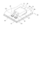
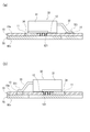
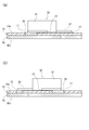
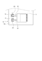
- FIG. It is an external view of the circuit structure concerning one Embodiment of this invention. It is the figure which expanded and showed the part by which the electronic component in the circuit structure was mounted. It is sectional drawing of a part (board
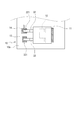
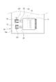
- FIG. It is a top view of the part in which the electronic component in the circuit structure was mounted. It is the top view which showed an example of the circuit structure body provided with the connection part isolate
- the plane direction in the following description refers to the plane direction of the substrate 10 and the conductive member 20, and the height direction (vertical direction) is a direction orthogonal to the plane direction (conductivity of the substrate 10).
- the surface on which the pattern is formed is the top).
- a circuit structure 1 As shown in FIG. 1, a circuit structure 1 according to an embodiment of the present invention includes a substrate 10, a conductive member 20, and an electronic component 30. Each configuration will be specifically described below with reference to FIGS.
- the substrate 10 has a conductive pattern (only a land 14 described later, which is a part of the conductive pattern) formed on one surface 10a (upper surface).
- the conductive path formed by the conductive pattern is a control conductive path (a part of the circuit), and the current flowing is smaller than the conductive path (a part of the circuit) formed by the conductive member 20.
- the conductive member 20 is a plate-like portion fixed to the other surface 10 b of the substrate 10.
- the conductive member 20 is formed in a predetermined shape by press working or the like, and constitutes a conductive path for electric power, which is a portion through which a relatively large current (larger than the conductive path constituted by the conductive pattern) flows.
- the conductive member 20 is also referred to as a bus bar (bus bar plate) or the like.
- the conductive member 20 is fixed to the other surface 10b of the substrate 10 through, for example, an insulating adhesive sheet, and the substrate 10 and the conductive member 20 are integrated (a set of the substrate 10 and the conductive member 20).
- the conductive pattern or the shape of the conductive path formed by the conductive member 20 may be any, the description thereof is omitted. Moreover, the shape of the whole board
- the electronic component 30 is an element mounted on the substrate 10 and has a main body portion 31 and a terminal portion of the element.
- the electronic component 30 in the present embodiment includes a first type terminal 32, a second type terminal 33, and a third type terminal 34 as terminal portions.
- An example of the electronic component 30 is a transistor (FET).
- the first type terminal 32 is a gate terminal
- the second type terminal 33 is a source terminal
- the third type terminal 34 is a drain terminal.
- the first type terminal 32 is connected to the conductive pattern of the substrate 10
- the second type terminal 33 is connected to the conductive member 20
- the third type terminal 34 is connected to the second type terminal 33 in the conductive member 20. It is connected to a part different from the part to be made.
- the electronic component 30 is described as having various terminals one by one. However, the electronic component 30 may have a plurality of certain terminals.
- the first type terminal 32 and the second type terminal 33 protrude from the side surface of the main body 31 having a substantially rectangular parallelepiped shape.
- the two terminals include a base end portion protruding along the planar direction, a portion bent downward from the tip of the base end portion, and the plane extending from the tip of the bent portion. And tip portions 321 and 331 extending in a similar manner.
- the heights (positions in the vertical direction) of the tip portions 321 and 331 that are soldered portions are substantially the same.
- the first type terminal 32 and the second type terminal 33 are formed in exactly the same shape. That is, the first type terminal 32 and the second type terminal 33 overlap each other when viewed from the direction along the surface on which the terminal in the main body 31 is provided.
- the third type terminal 34 is a plate-like portion provided on the bottom (lower surface) of the main body 31. That is, the third type terminal 34 is along the planar direction. It can be said that the third type terminal 34 is a part constituting at least a part of the bottom of the main body 31.
- Such an electronic component 30 is mounted on the substrate 10 (substrate 10 and conductive member 20 set) as follows.
- a first opening 11 penetrating the substrate 10 in the thickness direction is formed at a location where the electronic component 30 is mounted on the substrate 10.
- the first opening 11 is formed in a shape through which the main body 31 of the electronic component 30 cannot pass.
- the electronic component 30 is placed on one surface (surface on which a conductive pattern is formed) of the substrate 10 so that the main body portion 31 covers at least a part of the first opening 11.
- At least a part of the third type terminal 34 provided on the bottom of the main body 31 faces the first opening 11 (overlaps with the first opening 11 in the vertical direction).
- the main body 31 is placed on the one surface 10 a of the substrate 10 so as not to cover a part of the first opening 11.
- the main body 31 of the electronic component 30 is soldered to the conductive member 20 through the first opening 11. Since the third type terminal 34 is provided on the bottom of the main body 31, the third type terminal 34 is electrically connected to a predetermined portion (a portion facing the first opening 11) of the conductive member 20. That is, the main body 31 (third type terminal 34) provided so as to cover at least a part of the first opening 11 is soldered to the conductive member 20 through the first opening 11. The third type terminal 34 is electrically connected to the conductive member 20 while being physically connected to the conductive member 20 (the set of the substrate 10 and the conductive member 20).
- the electronic component 30 is disposed on the one surface 10a of the substrate 10. That is, the bottom of the main body 31 is a portion facing the first opening 11 (a portion overlapping the first opening 11 in the vertical direction). In other words, it includes a portion that contacts one surface 10 a of the substrate 10.
- the connection part 12 is provided in the part which the bottom of the main-body part 31 in the one surface 10a of the board
- the connection part 12 can be formed with the same material (for example, copper) as a conductive pattern. That is, it can be manufactured in the same process as the process of forming the conductive pattern.
- the connecting portion 12 is not electrically connected to the conductive pattern.
- the part of the main body 31 of the electronic component 30 that contacts the one surface 10a of the substrate 10 is soldered to the connecting part 12. That is, the main body 31 of the electronic component 30 is connected not only to the conductive member 20 but also to the substrate 10. Thereby, the physical connection of the electronic component 30 to the substrate 10 and the conductive member 20 set can be further strengthened.
- size and shape of the 1st opening 11 and the connection part 12 can be changed suitably. As shown in FIG. 4, it is good also as a structure which provided the substantially rectangular connection part 12 so that it might rank with the 1st opening 11, and as shown in FIG. 5, the structure in which the connection part 12 was separately provided in several places It is good. Since the first opening 11 is for connecting the main body 31 to the conductive member 20, and the connection portion 12 is for connecting the main body 31 to the substrate 10, the connection between the main body 31 and the conductive member 20 is performed. The shape, position, size, and the like of the first opening 11 and the connection portion 12 may be set according to the strength required for the connection between the main body portion 31 and the substrate 10.
- the tip portion 321 of the first type terminal 32 of the electronic component 30 is positioned on a predetermined portion in the conductive pattern.
- the first type terminal 32 is located on the land 14 (a part of the conductive pattern) to be connected.
- the first type terminal 32 is soldered to the land 14. That is, the first type terminal 32 is physically and electrically connected to the conductive pattern.
- a second opening 13 is formed in the substrate 10 so as to penetrate the substrate 10 in the thickness direction.
- the second opening 13 is formed at a position where the tip portion 331 of the second type terminal 33 overlaps in the vertical direction in a state where the electronic component 30 is placed at a predetermined position on the substrate 10.
- the height of the tip portion 321 of the first type terminal 32 and the tip portion 331 of the second type terminal 33 are substantially the same, and the tip portion 321 of the first type terminal 32 is one side of the substrate 10.
- the fact that it is located on the surface 10 a means that the tip portion 331 of the second type terminal 33 is located on the second opening 13.
- the second type terminal 33 positioned on the second opening 13 is soldered to a predetermined portion of the conductive member 20 through the second opening 13. That is, the second type terminal 33 is physically and electrically connected to the conductive member 20. Needless to say, the portion of the conductive member 20 to which the second type terminal 33 is connected and the portion of the conductive member 20 to which the third type terminal 34 is connected do not have direct electrical connection. The second type terminal 33 and the third type terminal 34 are not short-circuited). Moreover, in this embodiment, although the 1st opening 11 and the 2nd opening 13 are not connected, the opening in which both were united may be sufficient. However, when the solder in the first opening 11 and the solder in the second opening 13 come into contact with each other, a short circuit occurs.
- the mounting method of the electronic component 30 on the board 10 is not limited to a specific method, but the so-called reflow soldering method facilitates manufacture and quality. It is preferable in terms of stabilization.
- solder cream solder
- the circuit component 1 on which the electronic component 30 is mounted is obtained as described above by melting the solder while the electronic component 30 is placed at a predetermined position. If the electronic component 30 is mounted by such reflow soldering, the first opening 11 and the second opening 13 must be separated in order to prevent a short circuit between the second type terminal 33 and the third type terminal 34. Is preferred.
- the circuit structure 1 according to the present embodiment described above has the following operational effects.
- the circuit configuration body 1 according to the present embodiment is disposed on one surface 10a of the substrate 10 so that the main body 31 of the electronic component 30 covers at least a part of the first opening 11 formed in the substrate 10, Since the second type terminal 33 is connected to the conductive member 20 through the second opening 13 formed in the substrate 10, processing such as bending the terminal is not necessary. That is, the height of the tip portion 321 of the first type terminal 32 included in the electronic component 30 and the height of the tip portion 331 of the second type terminal 33 can be set substantially the same.
- the third type terminal 34 provided on the bottom of the main body 31 can be connected to the conductive member 20 through the first opening 11 together with the main body 31. Thereby, the physical connection of the electronic component 30 (main body part 31) and the conductive member 20, and the electrical connection of the third type terminal 34 and the conductive member 20 can be achieved at a time. Further, the heat generated in the main body 31 is efficiently radiated through the conductive member 20.
- the size of the first opening 11 formed in the substrate 10 is too large, when the electronic component 30 is displaced with respect to the first opening 11, a part of the main body 31 is in the first opening 11. There is a risk of getting stuck. For example, in the reflow soldering process (in a state before the electronic component 30 is soldered), a part of the main body 31 may enter the first opening 11 due to vibration or the like. On the other hand, if the size of the first opening 11 is made too small, the area of the main body portion 31 in contact with the solder in the first opening 11 becomes small. The reliability of the physical connection of the unit 31) may become a problem.
- connection portion 12 is provided in the vicinity of the location where the first opening 11 is formed in the substrate 10, and at least a part of the main body portion 31 is connected to the connection portion 12. Further, the reliability of physical connection of the electronic component 30 (main body portion 31) to the substrate 10 and the conductive member 20 set can be improved.
- the main body 31 of the electronic component 30 is placed on the one surface 10 a of the substrate 10 so as not to cover a part of the first opening 11, it is covered by the main body 31 in the first opening 11. It is possible to confirm whether or not the connection between the main body portion 31 and the conductive member 20 through the first opening 11 is ensured from the nonexistent portion (exposed portion).
- the first modification shown in FIG. 6 and FIG. 7 is such that a through hole 121 (through hole) penetrating the substrate 10 in the thickness direction is formed in a portion of the substrate 10 where the connection portion 12 is formed.
- a plurality of through holes 121 are preferably formed.
- Each through hole 121 is preferably formed with a so-called via.
- the third type terminal 34 provided on the bottom of the main body 31 contacts the connection part 12 provided on one surface 10 a of the substrate 10.
- the third type terminal 34 is soldered to the connection portion 12 and is also soldered to the conductive member 20 through the through hole 121. That is, the third type terminal 34 is electrically connected to the conductive member 20 by the solder applied in the through hole 121.
- the third type terminal 34 is connected to the conductive member 20 not only through the connection portion 12 but also through the through hole 121, the third type terminal 34 is connected not only through the first opening 11 but also through the through hole 121. Therefore, the reliability of electrical connection is improved. That is, in consideration of the provision of the connection portion 12 to which the main body portion 31 is connected, by forming the through hole 121 in the portion where the connection portion 12 is formed, the main body portion 31 and the substrate 10 by the connection portion 12 are formed. In addition to strengthening the physical connection, the electrical connection between the third type terminal 34 and the conductive member 20 can be enhanced.
- the second modification shown in FIG. 8 uses the electronic component 30 in which the first type terminal 32 ′ and the second type terminal 33 ′ are short.
- the main body 31 of the electronic component 30 has a structure that is disposed on the one surface 10a of the substrate 10 so as to cover at least a part of the first opening 11 formed in the substrate 10. It suffices that the first type terminal 32 ′ has a length that can reach the land 14 of the conductive pattern and the second type terminal 33 ′ reaches the second opening 13.
- each terminal may have a shape that extends straight from the main body 31.
- the present invention is also excellent in that the electronic component 30 having a short terminal that is difficult to bend can be used.
- connection portion 12 is not provided on the substrate 10. Since the main body 31 (the third type terminal 34) is connected to the conductive member 20 through the first opening 11, the connection between the main body 31 and the substrate 10 and the conductive member 20 can be achieved without providing the connection portion 12. Can do. If the connection part 12 is provided, since the magnitude
- the electronic component 30 in the above embodiment is provided with the terminal (third type terminal 34) on the bottom of the main body 31, the electronic device in which the terminal is not provided on the bottom in this way.
- the mounting method similar to the above can also be applied to the component 30. That is, the connection between the main body 31 and the conductive member 20 through the first opening 11 is not intended to be an electrical connection (to be a physical connection).
Landscapes
- Engineering & Computer Science (AREA)
- Microelectronics & Electronic Packaging (AREA)
- Manufacturing & Machinery (AREA)
- Structures For Mounting Electric Components On Printed Circuit Boards (AREA)
- Structure Of Printed Boards (AREA)
- Connection Or Junction Boxes (AREA)
- Printing Elements For Providing Electric Connections Between Printed Circuits (AREA)
Abstract
電子部品の端子の曲げ加工等が不要である回路構成体を提供すること。 実装される電子部品30は、その本体部31が基板10に形成された第一開口11の少なくとも一部を覆うように基板10の一方の面10a上に配置された状態で、当該第一開口11を通じて導電部材20に接続され、第一種端子32が基板10の導電パターン(ランド14)に接続され、第二種端子33が基板10に形成された第二開口13を通じて導電部材20に接続されている回路構成体1とする。
Description
本発明は、基板および導電部材を備えた回路構成体に関する。
比較的小さな電流を導通させる回路を構成する導電パターンが形成された基板に対し、比較的大きな電流を導通させるための回路を構成する導電部材が固定された回路構成体が公知である(例えば、下記特許文献1参照)。
この種の回路構成体には、基板に形成された導電パターンに接続される端子と、導電部材に接続される端子を有する電子部品を備えるものがある。このような電子部品を備える回路構成体では、導電パターン表面と導電部材表面の高さが異なるため、一方の端子を曲げる等して、当該高さの差を吸収する必要があった(特許文献1においては、図4等に示すように端子34と端子36の形状が異なる)。
本発明が解決しようとする課題は、上記のような電子部品の端子の曲げ加工等が不要である回路構成体を提供することにある。
上記課題を解決するために本発明にかかる回路構成体は、一方の面に導電パターンが形成された基板と、本体部およびこの本体部より突出した第一種端子および第二種端子を有し、前記基板の一方の面に実装される電子部品と、前記基板の他方の面に固定された導電路を構成する導電部材と、を備え、前記電子部品は、その本体部が前記基板に形成された第一開口の少なくとも一部を覆うように前記基板の一方の面上に配置された状態で、当該第一開口を通じて前記導電部材に接続され、前記第一種端子が前記基板の導電パターンに、前記第二種端子が前記基板に形成された第二開口を通じて前記導電部材に接続されていることを特徴とする。
前記第一種端子および前記第二種端子の先端部分は、略同じ高さに位置するとよい。
前記本体部の底には第三種端子が設けられており、当該第三種端子が前記本体部とともに前記第一開口を通じて前記導電部材に接続されているとよい。
前記基板の一方の面における前記第一開口が形成された箇所の近傍には接続部が設けられ、前記電子部品の本体部における前記基板の一方の面上に位置する部分の少なくとも一部は、前記接続部に接続されているとよい。
前記基板における前記接続部が形成された部分には貫通孔が形成されており、前記第三種端子は前記接続部に接続されるとともに、前記貫通孔を通じて前記導電部材にも接続されているとよい。
前記電子部品は、その本体部が前記第一開口の一部を覆わないようにして前記基板の一方の面上に配置されているとよい。
本発明にかかる回路構成体は、電子部品の本体部が基板に形成された第一開口の少なくとも一部を覆うように基板の一方の面上に配置され、第二種端子が基板に形成された第二開口を通じて導電部材に接続される構造であるため、端子を曲げる等の加工が不要となる。
電子部品が有する第一種端子の先端部分の高さと、第二種端子の先端部分の高さは、略同じに設定することができる。
本体部の底に設けられた第三種端子が本体部とともに第一開口を通じて導電部材に接続された構造とすることもできる。
第一開口の大きさを大きくしすぎると、第一開口に対して電子部品が位置ずれした場合、本体部の一部が第一開口内に入り込んだ状態となってしまうおそれがある。一方、第一開口の大きさを小さくしすぎると、基板および導電部材組に対する電子部品(本体部)の物理的な接続の信頼性が問題となるおそれがある。そのため、基板における第一開口が形成された箇所の近傍に接続部を設け、当該接続部に本体部の少なくとも一部が接続された構造とすることにより、基板および導電部材組に対する電子部品(本体部)の物理的な接続の信頼性を向上させることができる。
第三種端子が接続部だけでなく貫通孔を通じて導電部材に接続されていれば、第三種端子が第一開口だけでなく貫通孔を通じて導電部材に接続された構造となるため、電気的な接続の信頼性も向上する。
電子部品の本体部が第一開口の一部を覆わないようにして基板の一方の面上に配置された構造とすれば、第一開口における本体部に覆われていない部分(露出した部分)から、第一開口を通じた本体部と導電部材の接続が確実になされているかどうかを確認することができる。
以下、本発明の実施形態について図面を参照しつつ詳細に説明する。なお、特に明示した場合を除き、以下の説明における平面方向とは、基板10や導電部材20の平面方向をいい、高さ方向(上下方向)とは平面方向に直交する方向(基板10の導電パターンが形成された面を上とする)をいうものとする。
図1に示すように、本発明の一実施形態にかかる回路構成体1は、基板10、導電部材20および電子部品30を備える。以下、図1~図4を参照して各構成について具体的に説明する。
基板10は、一方の面10a(上側の面)に導電パターン(導電パターンの一部である後述するランド14のみ図示する)が形成されたものである。当該導電パターンが構成する導電路は制御用の導電路(回路の一部)であり、導電部材20が構成する導電路(回路の一部)よりも流れる電流が相対的に小さい。
導電部材20は、基板10の他方の面10bに固定された板状の部分である。導電部材20は、プレス加工等によって所定の形状に形成され、相対的に大きな(導電パターンによって構成される導電路よりも大きな)電流が流れる部分である電力用の導電路を構成する。導電部材20は、バスバー(バスバープレート)等とも称される。導電部材20は、例えば絶縁性の接着シートなどを介して、基板10の他方の面10bに固定され、基板10と導電部材20が一体化されている(基板10・導電部材20組)。導電パターンや導電部材20が構成する導電路の形状はどのようなものであってもよいため、説明を省略する。また、基板10や導電部材20全体の形状も適宜変更可能である。なお、図1に示した導電部材20の外側の枠は最終的には切り落とされることとなる。
電子部品30は、基板10に実装される素子であって、素子の本体部31および端子部を有する。本実施形態における電子部品30は、端子部として第一種端子32、第二種端子33、および第三種端子34を有する。電子部品30の一例としては、トランジスタ(FET)が挙げられる。この場合、第一種端子32はゲート端子であり、第二種端子33はソース端子であり、第三種端子34はドレイン端子である。後述するように、第一種端子32は基板10の導電パターンに接続され、第二種端子33は導電部材20に接続され、第三種端子34は導電部材20における第二種端子33が接続される部位とは異なる部位に接続される。なお、以下では、電子部品30は、各種端子を一つずつ有しているものとして説明するが、ある種の端子を複数有するものであってもよい。
第一種端子32および第二種端子33は、略直方体形状の本体部31の側面より突出している。具体的には、両端子は、平面方向に沿って突出した基端側部分と、基端側部分の先端から下方に向かうように屈曲した部分と、当該屈曲した部分の先端から平面方向に沿うように延びる先端部分321、331とを有する。はんだ付けされる部分である先端部分321、331の高さ(上下方向における位置)は略同じである。本実施形態では、第一種端子32と第二種端子33は全く同形状に形成されている。つまり、本体部31における端子が設けられた面に沿う方向から見て、第一種端子32と第二種端子33は重なる。
第三種端子34は、本体部31の底(下面)に設けられた板状の部分である。つまり、第三種端子34は平面方向に沿う。第三種端子34は、本体部31の底の少なくとも一部を構成する部分であるともいえる。
このような電子部品30は、次のように基板10(基板10・導電部材20組)に実装される。基板10における電子部品30が実装される箇所には、基板10を厚み方向に貫く第一開口11が形成されている。第一開口11は、電子部品30の本体部31が通過することのできない形状に形成されている。電子部品30は、その本体部31が第一開口11の少なくとも一部を覆うように、基板10の一方側の面(導電パターンが形成された面)上に載置される。本体部31の底に設けられた第三種端子34の少なくとも一部は、第一開口11に臨む(上下方向において第一開口11に重なる)。本実施形態では、本体部31が第一開口11の一部を覆わないようにして基板10の一方の面10a上に載置される。
かかる第一開口11を通じて、電子部品30の本体部31は導電部材20にはんだ付けされている。本体部31の底には第三種端子34が設けられているため、第三種端子34は導電部材20の所定箇所(第一開口11に臨む部分)と電気的に接続される。つまり、第一開口11の少なくとも一部を覆うように設けられた本体部31(第三種端子34)が、当該第一開口11を通じて導電部材20にはんだ付けされることにより、本体部31が物理的に導電部材20(基板10・導電部材20組)に接続されるとともに、第三種端子34が電気的に導電部材20に接続される。
このように電子部品30が基板10の一方の面10a上に配置されるということは、本体部31の底は、第一開口11に臨む部分(上下方向において第一開口11と重なる部分)と、基板10の一方の面10aに接触する部分を含む、ということである。本実施形態では、基板10の一方の面10aにおける本体部31の底が接触する部分に接続部12が設けられている。つまり、接続部12は、第一開口11の近傍に設けられている。接続部12は、導電パターンと同じ材料(例えば銅)で形成することができる。つまり、導電パターンを形成する工程と同じ工程で作製することができる。なお、接続部12は導電パターンと電気的に接続されていない。
電子部品30の本体部31における基板10の一方の面10aに接触する部分は、かかる接続部12にはんだ付けされている。つまり、電子部品30の本体部31は、導電部材20だけでなく、基板10にも接続されている。これにより、基板10・導電部材20組に対する電子部品30の物理的な接続をより強固なものとすることができる。
なお、第一開口11や接続部12の大きさや形状は適宜変更可能である。図4に示すように第一開口11に並ぶように略方形状の接続部12を設けた構造としてもよいし、図5に示すように接続部12が複数個所に分離して設けられた構造としてもよい。第一開口11は本体部31を導電部材20に接続するためのものであり、接続部12は本体部31を基板10に接続するためのものであるため、本体部31と導電部材20の接続、本体部31と基板10の接続に求められる強度等に応じて、第一開口11および接続部12の形状、位置、大きさ等を設定すればよい。
電子部品30が基板10における所定位置に載置された状態において、電子部品30の第一種端子32の先端部分321は、導電パターンにおける所定部位上に位置する。具体的には、第一種端子32を接続すべきランド14(導電パターンの一部)の上に位置する。第一種端子32は、かかるランド14にはんだ付けされている。つまり、第一種端子32は、導電パターンに物理的かつ電気的に接続されている。
また、基板10には、当該基板10を厚み方向に貫く第二開口13が形成されている。第二開口13は、電子部品30が基板10における所定位置に載置された状態において、第二種端子33の先端部分331が上下方向に重なるような位置に形成される。具体的には、第一種端子32の先端部分321と、第二種端子33の先端部分331の高さは略同じであるのであり、第一種端子32の先端部分321が基板10の一方の面10a上に位置するということは、第二種端子33の先端部分331は第二開口13の上に位置するということである。このように第二開口13の上に位置する第二種端子33は、当該第二開口13を通じて導電部材20の所定部位にはんだ付けされている。つまり、第二種端子33は導電部材20に物理的かつ電気的に接続されている。なお、当然ではあるが、導電部材20における第二種端子33が接続される部位と、第三種端子34が接続される部位は、直接的な電気的な接続が存在するものではない(第二種端子33と第三種端子34がショートするものではない)。また、本実施形態では、第一開口11と第二開口13は繋がっていないが、両者が一体となった開口であってもよい。ただし、第一開口11内のはんだと第二開口13内のはんだが接触するとショートしてしまうため、両開口は区切られていることが好ましい。
このような基板10(基板10・導電部材20組)に対する電子部品30の実装方法は、特定の方法に限定されるわけではないが、いわゆるリフローはんだ付け方法により行うことが製造の容易化、品質安定化等の面で好ましい。リフローはんだ付け方法を用いて製造する場合には、基板10・導電部材20組における第一開口11内、第二開口13内、接続部12上、ランド14上に予めはんだ(クリームはんだ)を塗布(印刷)しておき、所定位置に電子部品30を載置した状態ではんだを溶融させることで、上記のように電子部品30が実装された回路構成体1が得られる。このようなリフローはんだ付けによって電子部品30を実装するのであれば、第二種端子33と第三種端子34のショートを防止するため、第一開口11と第二開口13は区切られていることが好ましい。
以上説明した本実施形態にかかる回路構成体1によれば次のような作用効果が奏される。本実施形態にかかる回路構成体1は、電子部品30の本体部31が基板10に形成された第一開口11の少なくとも一部を覆うように基板10の一方の面10a上に配置され、第二種端子33が基板10に形成された第二開口13を通じて導電部材20に接続される構造であるため、端子を曲げる等の加工が不要となる。つまり、電子部品30が有する第一種端子32の先端部分321の高さと、第二種端子33の先端部分331の高さを、略同じに設定することができる。
また、本体部31の底に設けられた第三種端子34を、本体部31とともに第一開口11を通じて導電部材20に接続することができる。これにより、電子部品30(本体部31)と導電部材20の物理的な接続、第三種端子34と導電部材20の電気的な接続を一度に図ることができる。また、本体部31に生じる熱が導電部材20を通じて効率よく放熱される構造となる。
また、基板10に形成される第一開口11の大きさを大きくしすぎると、第一開口11に対して電子部品30が位置ずれした場合、本体部31の一部が第一開口11内に入り込んだ状態となってしまうおそれがある。例えば、上記リフローはんだ付け工程において(電子部品30がはんだ付けされる前の状態において)、振動等によって本体部31の一部が第一開口11内に入り込んでしまうおそれがある。一方、第一開口11の大きさを小さくしすぎると、本体部31における第一開口11内のはんだに接触する部分の面積が小さくなるから、基板10・導電部材20組に対する電子部品30(本体部31)の物理的な接続の信頼性が問題となってしまうおそれがある。これに対し本実施形態では、基板10における第一開口11が形成された箇所の近傍に接続部12を設け、当該接続部12に本体部31の少なくとも一部が接続された構造とされるから、基板10および導電部材20組に対する電子部品30(本体部31)の物理的な接続の信頼性を向上させることができる。
また、電子部品30の本体部31が第一開口11の一部を覆わないようにして基板10の一方の面10a上に載置されるため、第一開口11における本体部31に覆われていない部分(露出した部分)から、第一開口11を通じた本体部31と導電部材20の接続が確実になされているかどうかを確認することができる。
上記本発明の一実施形態にかかる回路構成体1の変形例として、以下のような例が考えられる。
図6および図7に示す第一変形例は、基板10における接続部12が形成された部分に、基板10を厚み方向に貫く貫通孔121(スルーホール)が形成されたものである。貫通孔121は、複数形成されていることが好ましい。また、各貫通孔121にはいわゆるビアが形成されていることが好ましい。本例において、本体部31の底に設けられた第三種端子34は、基板10の一方の面10aに設けられた接続部12に接触する。そして、かかる第三種端子34は、接続部12にはんだ付けされるとともに、貫通孔121を通じて導電部材20にもはんだ付けされている。つまり、第三種端子34は、貫通孔121内に塗布されたはんだによって、導電部材20に電気的に接続されている。このように、第三種端子34が接続部12だけでなく貫通孔121を通じて導電部材20に接続されていれば、第三種端子34が第一開口11だけでなく貫通孔121を通じて導電部材20に接続された構造となるため、電気的接続の信頼性も向上する。つまり、本体部31が接続される接続部12が設けられることを踏まえ、当該接続部12が形成された部分に貫通孔121を形成しておくことにより、接続部12による本体部31と基板10の物理的な接続の強化だけでなく、第三種端子34と導電部材20の電気的な接続の強化を図ることができる。
図8に示す第二変形例は、第一種端子32’および第二種端子33’の長さが短い電子部品30を用いたものである。上述したように、電子部品30の本体部31は、基板10に形成された第一開口11の少なくとも一部を覆うように基板10の一方の面10a上に配置される構造であるから、第一種端子32’は導電パターンのランド14まで、第二種端子33’は第二開口13まで届くような長さを有しておりさえすればよい。図示されるように、各端子は、本体部31から真っすぐ直線状に延びる形状であってもよい。このように、本発明は、曲げることが困難な短い端子を有する電子部品30を用いることができるという点においても優れるものである。
図9に示す第三変形例は、基板10上に接続部12が設けられていない構成である。本体部31(第三種端子34)は、第一開口11を通じて導電部材20に接続されるから、接続部12を設けなくても本体部31と基板10・導電部材20組の接続を図ることができる。接続部12を設けていれば、その分第一開口11の大きさを小さくすることができるため、本体部31の一部が第一開口11内に入り込んでしまうおそれを低減することができるという利点がある。
以上、本発明の実施形態について詳細に説明したが、本発明は上記実施形態に何ら限定されるものではなく、本発明の要旨を逸脱しない範囲で種々の改変が可能である。
例えば、上記実施形態における電子部品30は、本体部31の底に端子(第三種端子34)が設けられたものであることを説明したが、このように底に端子が設けられていない電子部品30についても上記と同様の実装手法が適用できる。つまり、第一開口11を通じた本体部31と導電部材20の接続が、電気的な接続を図るものではなくなる(物理的な接続を図るものとなる)だけである。
Claims (6)
- 一方の面に導電パターンが形成された基板と、
本体部およびこの本体部より突出した第一種端子および第二種端子を有し、前記基板の一方の面に実装される電子部品と、
前記基板の他方の面に固定された導電路を構成する導電部材と、
を備え、
前記電子部品は、その本体部が前記基板に形成された第一開口の少なくとも一部を覆うように前記基板の一方の面上に配置された状態で、当該第一開口を通じて前記導電部材に接続され、
前記第一種端子が前記基板の導電パターンに、前記第二種端子が前記基板に形成された第二開口を通じて前記導電部材に接続されていることを特徴とする回路構成体。 - 前記第一種端子および前記第二種端子の先端部分は、略同じ高さに位置することを特徴とする請求項1に記載の回路構成体。
- 前記本体部の底には第三種端子が設けられており、当該第三種端子が前記本体部とともに前記第一開口を通じて前記導電部材に接続されていることを特徴とする請求項1または請求項2に記載の回路構成体。
- 前記基板の一方の面における前記第一開口が形成された箇所の近傍には接続部が設けられ、
前記電子部品の本体部における前記基板の一方の面上に位置する部分の少なくとも一部は、前記接続部に接続されていることを特徴とする請求項1から請求項3のいずれか一項に記載の回路構成体。 - 前記基板における前記接続部が形成された部分には貫通孔が形成されており、
前記第三種端子は前記接続部に接続されるとともに、前記貫通孔を通じて前記導電部材にも接続されていることを特徴とする請求項3を引用する請求項4に記載の回路構成体。 - 前記電子部品は、その本体部が前記第一開口の一部を覆わないようにして前記基板の一方の面上に配置されていることを特徴とする請求項1から請求項5のいずれか一項に記載の回路構成体。
Priority Applications (3)
| Application Number | Priority Date | Filing Date | Title |
|---|---|---|---|
| US15/326,870 US9974182B2 (en) | 2014-07-22 | 2015-07-01 | Circuit assembly |
| CN201580036745.6A CN106471870B (zh) | 2014-07-22 | 2015-07-01 | 电路结构体 |
| DE112015003374.2T DE112015003374B4 (de) | 2014-07-22 | 2015-07-01 | Schaltungsanordnung |
Applications Claiming Priority (2)
| Application Number | Priority Date | Filing Date | Title |
|---|---|---|---|
| JP2014-148721 | 2014-07-22 | ||
| JP2014148721A JP6287659B2 (ja) | 2014-07-22 | 2014-07-22 | 回路構成体 |
Publications (1)
| Publication Number | Publication Date |
|---|---|
| WO2016013362A1 true WO2016013362A1 (ja) | 2016-01-28 |
Family
ID=55162894
Family Applications (1)
| Application Number | Title | Priority Date | Filing Date |
|---|---|---|---|
| PCT/JP2015/069019 Ceased WO2016013362A1 (ja) | 2014-07-22 | 2015-07-01 | 回路構成体 |
Country Status (5)
| Country | Link |
|---|---|
| US (1) | US9974182B2 (ja) |
| JP (1) | JP6287659B2 (ja) |
| CN (1) | CN106471870B (ja) |
| DE (1) | DE112015003374B4 (ja) |
| WO (1) | WO2016013362A1 (ja) |
Families Citing this family (4)
| Publication number | Priority date | Publication date | Assignee | Title |
|---|---|---|---|---|
| JP2018098369A (ja) | 2016-12-14 | 2018-06-21 | 株式会社オートネットワーク技術研究所 | 回路構成体 |
| JP7001960B2 (ja) * | 2018-03-23 | 2022-01-20 | 株式会社オートネットワーク技術研究所 | 回路構成体 |
| JP7024704B2 (ja) * | 2018-12-28 | 2022-02-24 | 住友電装株式会社 | 電子モジュール |
| JP7528573B2 (ja) * | 2020-07-01 | 2024-08-06 | 株式会社オートネットワーク技術研究所 | 回路構成体 |
Citations (8)
| Publication number | Priority date | Publication date | Assignee | Title |
|---|---|---|---|---|
| JPS6413788A (en) * | 1987-07-07 | 1989-01-18 | Fujitsu Ltd | Printed board |
| JPH0338653U (ja) * | 1989-08-24 | 1991-04-15 | ||
| JPH0685427A (ja) * | 1992-09-03 | 1994-03-25 | Ibiden Co Ltd | 半導体パッケージ搭載基板 |
| JPH0645393U (ja) * | 1992-11-27 | 1994-06-14 | 株式会社東芝 | 発熱素子の放熱構造 |
| JPH07336009A (ja) * | 1994-06-10 | 1995-12-22 | Fujitsu General Ltd | 半導体素子の放熱構造 |
| JP2003318579A (ja) * | 2002-04-24 | 2003-11-07 | Toyoda Mach Works Ltd | 放熱板付きfetの放熱方法 |
| JP2004349418A (ja) * | 2003-05-21 | 2004-12-09 | Nec Saitama Ltd | 表面実装部品の実装構造、実装方法およびリペア方法 |
| JP2006005096A (ja) * | 2004-06-16 | 2006-01-05 | Auto Network Gijutsu Kenkyusho:Kk | 回路構成体 |
Family Cites Families (25)
| Publication number | Priority date | Publication date | Assignee | Title |
|---|---|---|---|---|
| FR2588122B1 (fr) * | 1985-10-01 | 1988-06-24 | Radiotechnique Compelec | Dispositif semi-conducteur de puissance pour montage en surface |
| JPH0258393U (ja) * | 1988-10-19 | 1990-04-26 | ||
| DE4326506A1 (de) * | 1993-08-06 | 1995-02-09 | Bosch Gmbh Robert | Elektrisches Gerät, insbesondere Schalt- oder Steuergerät für Kraftfahrzeuge |
| EP0667736B1 (en) * | 1994-01-12 | 1996-12-18 | MAGNETEK S.p.A. | Laminar board for the production of printed circuits, printed circuit made with the said board, and method for its fabrication |
| DE19601649A1 (de) * | 1996-01-18 | 1997-07-24 | Telefunken Microelectron | Anordnung zur Verbesserung der Wärmeableitung bei elektrischen und elektronischen Bauelementen |
| JP3855306B2 (ja) * | 1996-05-30 | 2006-12-06 | 松下電器産業株式会社 | 電子部品搭載用放熱基板及びその製造方法 |
| DE19830576A1 (de) * | 1998-07-08 | 2000-01-13 | Iro Patent Ag Baar | Fadenbearbeitungssystem |
| FR2802714B1 (fr) * | 1999-12-21 | 2002-03-08 | Sagem | Module electrique de puissance et procede pour sa fabrication |
| US6421253B1 (en) * | 2000-09-08 | 2002-07-16 | Powerwave Technologies, Inc. | Durable laminated electronics assembly using epoxy preform |
| JP3927017B2 (ja) * | 2001-11-26 | 2007-06-06 | 株式会社オートネットワーク技術研究所 | 回路構成体及びその製造方法 |
| JP3929781B2 (ja) * | 2002-01-28 | 2007-06-13 | 株式会社オートネットワーク技術研究所 | 回路構成体 |
| JP4002427B2 (ja) * | 2001-11-26 | 2007-10-31 | 株式会社オートネットワーク技術研究所 | 回路構成体の製造方法 |
| FR2839417B1 (fr) * | 2002-05-03 | 2004-07-16 | Dav | Dispositif de commutation de puissance refroidi |
| JP2004253759A (ja) * | 2002-12-24 | 2004-09-09 | Auto Network Gijutsu Kenkyusho:Kk | 制御回路基板及び回路構成体 |
| JP4155048B2 (ja) * | 2003-02-14 | 2008-09-24 | 住友電装株式会社 | パワーモジュール及びその製造方法 |
| JP4076459B2 (ja) * | 2003-03-12 | 2008-04-16 | 株式会社オートネットワーク技術研究所 | バスバー構成板及びこれを用いた回路構成体の製造方法 |
| JP2005340684A (ja) * | 2004-05-31 | 2005-12-08 | Calsonic Kansei Corp | 基板への電子素子の取付構造 |
| SE529673C2 (sv) * | 2004-09-20 | 2007-10-16 | Danaher Motion Stockholm Ab | Kretsarrangemang för kylning av ytmonterade halvledare |
| JP4387290B2 (ja) * | 2004-11-29 | 2009-12-16 | 株式会社オートネットワーク技術研究所 | 回路構成体 |
| JP2007027584A (ja) * | 2005-07-20 | 2007-02-01 | Auto Network Gijutsu Kenkyusho:Kk | 接続構造、回路構成体、およびその製造方法 |
| JP2007180201A (ja) * | 2005-12-27 | 2007-07-12 | Yamaha Corp | 半導体装置 |
| US8927872B2 (en) * | 2009-02-20 | 2015-01-06 | Telefonaktiebolaget L M Ericsson (Publ) | Thermal pad and method of forming the same |
| JP5418851B2 (ja) * | 2010-09-30 | 2014-02-19 | 株式会社デンソー | 電子制御ユニット |
| JP2013115338A (ja) * | 2011-11-30 | 2013-06-10 | Sumitomo Wiring Syst Ltd | ダイオードの取付構造 |
| US9439412B2 (en) * | 2012-01-10 | 2016-09-13 | Richard Kittelson | Motion activated non-lethal animal trap |
-
2014
- 2014-07-22 JP JP2014148721A patent/JP6287659B2/ja active Active
-
2015
- 2015-07-01 US US15/326,870 patent/US9974182B2/en active Active
- 2015-07-01 DE DE112015003374.2T patent/DE112015003374B4/de active Active
- 2015-07-01 WO PCT/JP2015/069019 patent/WO2016013362A1/ja not_active Ceased
- 2015-07-01 CN CN201580036745.6A patent/CN106471870B/zh active Active
Patent Citations (8)
| Publication number | Priority date | Publication date | Assignee | Title |
|---|---|---|---|---|
| JPS6413788A (en) * | 1987-07-07 | 1989-01-18 | Fujitsu Ltd | Printed board |
| JPH0338653U (ja) * | 1989-08-24 | 1991-04-15 | ||
| JPH0685427A (ja) * | 1992-09-03 | 1994-03-25 | Ibiden Co Ltd | 半導体パッケージ搭載基板 |
| JPH0645393U (ja) * | 1992-11-27 | 1994-06-14 | 株式会社東芝 | 発熱素子の放熱構造 |
| JPH07336009A (ja) * | 1994-06-10 | 1995-12-22 | Fujitsu General Ltd | 半導体素子の放熱構造 |
| JP2003318579A (ja) * | 2002-04-24 | 2003-11-07 | Toyoda Mach Works Ltd | 放熱板付きfetの放熱方法 |
| JP2004349418A (ja) * | 2003-05-21 | 2004-12-09 | Nec Saitama Ltd | 表面実装部品の実装構造、実装方法およびリペア方法 |
| JP2006005096A (ja) * | 2004-06-16 | 2006-01-05 | Auto Network Gijutsu Kenkyusho:Kk | 回路構成体 |
Also Published As
| Publication number | Publication date |
|---|---|
| US20170202088A1 (en) | 2017-07-13 |
| JP6287659B2 (ja) | 2018-03-07 |
| CN106471870A (zh) | 2017-03-01 |
| DE112015003374T5 (de) | 2017-04-13 |
| US9974182B2 (en) | 2018-05-15 |
| JP2016025228A (ja) | 2016-02-08 |
| CN106471870B (zh) | 2019-06-18 |
| DE112015003374B4 (de) | 2023-08-03 |
Similar Documents
| Publication | Publication Date | Title |
|---|---|---|
| JP6330690B2 (ja) | 基板ユニット | |
| JP6477567B2 (ja) | 回路構成体 | |
| JP6287659B2 (ja) | 回路構成体 | |
| JP6504022B2 (ja) | 回路構成体 | |
| JP2015047031A (ja) | 回路構成体 | |
| US9899818B2 (en) | Circuit assembly and electrical junction box | |
| US10285274B2 (en) | Circuit structure | |
| US10062633B2 (en) | Substrate unit | |
| US9831583B2 (en) | Connector | |
| CN107211533B (zh) | 电路结构体 | |
| US10149386B2 (en) | Circuit assembly | |
| JP2017059560A (ja) | 回路構成体 | |
| JP4708941B2 (ja) | 接続構造、および回路構成体 | |
| KR20150109713A (ko) | 인쇄회로기판 어셈블리 | |
| JP6350867B2 (ja) | バスバー回路体の電子部品実装構造 | |
| JP2017135817A (ja) | 電気接続箱 | |
| WO2016125544A1 (ja) | 回路構成体 | |
| JP2014013809A (ja) | 半導体デバイス | |
| JP2016066467A (ja) | 車載用電子部品 | |
| JP2008210915A (ja) | プリント配線基板のグランド接続装置 |
Legal Events
| Date | Code | Title | Description |
|---|---|---|---|
| 121 | Ep: the epo has been informed by wipo that ep was designated in this application |
Ref document number: 15824732 Country of ref document: EP Kind code of ref document: A1 |
|
| WWE | Wipo information: entry into national phase |
Ref document number: 15326870 Country of ref document: US |
|
| WWE | Wipo information: entry into national phase |
Ref document number: 112015003374 Country of ref document: DE |
|
| 122 | Ep: pct application non-entry in european phase |
Ref document number: 15824732 Country of ref document: EP Kind code of ref document: A1 |