WO2016013305A1 - 炭化珪素半導体装置の製造方法 - Google Patents
炭化珪素半導体装置の製造方法 Download PDFInfo
- Publication number
- WO2016013305A1 WO2016013305A1 PCT/JP2015/066078 JP2015066078W WO2016013305A1 WO 2016013305 A1 WO2016013305 A1 WO 2016013305A1 JP 2015066078 W JP2015066078 W JP 2015066078W WO 2016013305 A1 WO2016013305 A1 WO 2016013305A1
- Authority
- WO
- WIPO (PCT)
- Prior art keywords
- electrode film
- silicon carbide
- carbide semiconductor
- nickel
- semiconductor device
- Prior art date
- Legal status (The legal status is an assumption and is not a legal conclusion. Google has not performed a legal analysis and makes no representation as to the accuracy of the status listed.)
- Ceased
Links
Images



Classifications
-
- H—ELECTRICITY
- H10—SEMICONDUCTOR DEVICES; ELECTRIC SOLID-STATE DEVICES NOT OTHERWISE PROVIDED FOR
- H10D—INORGANIC ELECTRIC SEMICONDUCTOR DEVICES
- H10D64/00—Electrodes of devices having potential barriers
- H10D64/01—Manufacture or treatment
- H10D64/011—Manufacture or treatment of electrodes ohmically coupled to a semiconductor
- H10D64/0111—Manufacture or treatment of electrodes ohmically coupled to a semiconductor to Group IV semiconductors
- H10D64/0115—Manufacture or treatment of electrodes ohmically coupled to a semiconductor to Group IV semiconductors to silicon carbide
-
- H—ELECTRICITY
- H10—SEMICONDUCTOR DEVICES; ELECTRIC SOLID-STATE DEVICES NOT OTHERWISE PROVIDED FOR
- H10D—INORGANIC ELECTRIC SEMICONDUCTOR DEVICES
- H10D62/00—Semiconductor bodies, or regions thereof, of devices having potential barriers
- H10D62/80—Semiconductor bodies, or regions thereof, of devices having potential barriers characterised by the materials
- H10D62/83—Semiconductor bodies, or regions thereof, of devices having potential barriers characterised by the materials being Group IV materials, e.g. B-doped Si or undoped Ge
- H10D62/832—Semiconductor bodies, or regions thereof, of devices having potential barriers characterised by the materials being Group IV materials, e.g. B-doped Si or undoped Ge being Group IV materials comprising two or more elements, e.g. SiGe
- H10D62/8325—Silicon carbide
-
- H—ELECTRICITY
- H10—SEMICONDUCTOR DEVICES; ELECTRIC SOLID-STATE DEVICES NOT OTHERWISE PROVIDED FOR
- H10D—INORGANIC ELECTRIC SEMICONDUCTOR DEVICES
- H10D8/00—Diodes
- H10D8/01—Manufacture or treatment
- H10D8/051—Manufacture or treatment of Schottky diodes
-
- H—ELECTRICITY
- H10—SEMICONDUCTOR DEVICES; ELECTRIC SOLID-STATE DEVICES NOT OTHERWISE PROVIDED FOR
- H10D—INORGANIC ELECTRIC SEMICONDUCTOR DEVICES
- H10D8/00—Diodes
- H10D8/60—Schottky-barrier diodes
Definitions
- the present invention relates to a method for manufacturing a silicon carbide semiconductor device.
- SiC silicon carbide
- SiC silicon carbide
- MOSFETs Metal Oxide Semiconductor Field Transistors
- SiC semiconductors have the advantage of lower on-resistance than high breakdown voltage MOSFETs using silicon (Si) semiconductors.
- Si silicon
- the on-resistance and switching speed of a power device are in a trade-off relationship, but a power device using an SiC semiconductor may be able to achieve both low on-resistance and high switching speed at the same time.
- the contact resistance of the ohmic contact is also a serious problem in increasing the switching speed of a power device using a SiC semiconductor.
- One of the problems in the practical application of power devices using SiC semiconductors is that a technique for forming a practical low-resistance ohmic contact suitable for each device structure and manufacturing (manufacturing) process has not been established. Can be mentioned.
- an ohmic electrode structure formed by depositing an electrode film on the n-type SiC semiconductor portion is 800 ° C. to 1200 ° C.
- a method of heat treatment at a high temperature of about 0 ° C. has been proposed (see, for example, Patent Documents 1 to 3 below).
- Nickel (Ni), tungsten (W), titanium (Ti), and the like are known as electrode materials.
- a practical contact resistance value of 10 ⁇ 6 ⁇ cm 2 is obtained, which makes a very promising ohmic contact.
- the nickel film reacts with the SiC semiconductor portion by high-temperature heat treatment, and a conductive reaction layer in which nickel-silicon-carbon (C) is mixed as the electrode film (for example, nickel silicide (NiSi) ) Film) is formed.
- C nickel-silicon-carbon
- NiSi nickel silicide
- many carbon atoms liberated (diffused) from the SiC semiconductor portion are deposited near the surface of the electrode film, and the surface of the electrode film is almost covered with a carbon layer formed by the deposition of carbon atoms.
- the adhesion between the electrode film and, for example, an aluminum (Al) film (wiring layer) for wiring to be further laminated (formed) on the electrode film is deteriorated, and the wiring layer may be peeled off.
- Patent Document 1 discloses that a carbon layer deposited on the surface of a nickel silicide film by the formation of a nickel silicide film serving as an electrode film is subjected to a heat treatment before a wiring layer is stacked on the nickel silicide film. It is described to be removed.
- Patent Documents 2 and 3 the material composition ratio of the electrode film is adjusted, and the carbide is generated by reacting the carbon film liberated from the SiC semiconductor part and the electrode film when forming the ohmic contact between the electrode film and the SiC semiconductor part. By doing so, it is described that the deposition of carbon atoms on the electrode film surface is suppressed.
- JP 2013-222823 A International Publication No. 2011/115294 JP 2013-219150 A
- the present invention can ensure the adhesion between the electrode film forming an ohmic contact with the SiC semiconductor portion and the wiring layer laminated on the electrode film.
- An object of the present invention is to provide a method for manufacturing a silicon semiconductor device.
- a silicon carbide semiconductor device manufacturing method includes an n-type silicon carbide semiconductor portion and a surface formed on the surface of the silicon carbide semiconductor portion.
- a method of manufacturing a silicon carbide semiconductor device that forms an ohmic contact with an electrode film and has the following characteristics. First, a first formation step is performed in which a first electrode film made of nickel is formed on the surface of the silicon carbide semiconductor portion as the surface electrode film. Next, a second formation step is performed in which a second electrode film made of nickel silicide is formed on the surface of the first electrode film as the surface electrode film.
- the silicon carbide semiconductor portion and the surface electrode film are silicided by reacting silicon atoms of the silicon carbide semiconductor portion with nickel atoms of the first electrode film by heat treatment.
- a heat treatment step for forming the ohmic contact is performed.
- carbon atoms that are liberated from the silicon carbide semiconductor portion and diffuse to the surface electrode film side are inside the second electrode film.
- the first electrode film is formed in a thin thickness with a small content that can be incorporated into the film.
- the surface electrode film of the carbon atoms taken into the second electrode film in the heat treatment step The second electrode film having a thickness capable of suppressing deposition on the surface is formed.
- the second electrode film in the second formation step, has a composition capable of suppressing a reaction with the silicon carbide semiconductor portion in the heat treatment step. It is characterized by forming.
- the second electrode film includes a nickel atom content of 60 atm% and a silicon atom content of 40 atm%, a nickel atom of 70 atm% and silicon. It is characterized in that the composition is in the range between 30 atom% content of atoms.
- the second formation step in the above-described invention, has a composition substantially equal to the composition of the first electrode film silicided in the heat treatment step. An electrode film is formed.
- the method for manufacturing a silicon carbide semiconductor device according to the present invention is characterized in that, in the above-described invention, the thickness of the first electrode film is not less than 5 nm and not more than 10 nm.
- the method for manufacturing a silicon carbide semiconductor device according to the present invention is characterized in that, in the above-described invention, the thickness of the second electrode film is 80 nm or more.
- the region of the surface electrode film that is silicided by the reaction with the silicon atoms in the silicon carbide semiconductor portion can be limited to the first electrode film, and the excess carbon atoms generated during the heat treatment are reduced. Can be made. In addition, the surplus carbon atoms can be taken into the second electrode film. For this reason, precipitation of carbon atoms on the outermost surface of the surface electrode film is suppressed.
- the method for manufacturing a silicon carbide semiconductor device when forming an ohmic contact by heat treatment, the deposition of carbon atoms on the surface of the electrode film is suppressed, and the adhesion with the wiring layer laminated on the electrode film is improved. There is an effect that it can be secured.
- FIG. 1 is a flowchart showing an outline of a method for manufacturing a silicon carbide semiconductor device according to an embodiment.
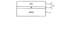
- FIG. 2 is a cross-sectional view showing a state during the manufacture of the silicon carbide semiconductor device according to the embodiment.
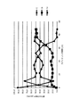
- FIG. 3 is a characteristic diagram showing the element distribution in the depth direction of the surface electrode film in Conventional Example 1.
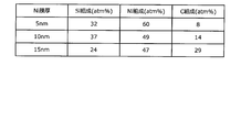
- FIG. 4 is a table showing the thickness (Ni film thickness) of the first electrode film and the surface composition of the first electrode film after heat treatment in Example 1.
- FIG. 5 is a chart showing the thickness of the second electrode film (NiSi film thickness) and the surface composition of the second electrode film in Example 2.
- 6 is a characteristic diagram showing element analysis in the depth direction of the surface electrode film in Example 2.
- FIG. 1 is a flowchart showing an outline of a method for manufacturing a silicon carbide semiconductor device according to an embodiment.
- FIG. 2 is a cross-sectional view showing a state during the manufacture of the silicon carbide semiconductor device according to the embodiment.
- FIG. 1 is a flowchart showing an outline of a method for manufacturing a silicon carbide semiconductor device according to an embodiment.
- FIG. 2 is a cross-sectional view showing a state during the manufacture of the silicon carbide semiconductor device according to the embodiment.
- FIG. 2 shows a state immediately after the surface electrode film 4 formed by sequentially laminating the first and second electrode films 2 and 3 on the n-type SiC semiconductor portion 1 is shown.
- the n-type SiC semiconductor unit 1 is, for example, an n-type semiconductor substrate made of an n-type SiC semiconductor (hereinafter referred to as an SiC substrate), an n-type SiC semiconductor layer stacked on the SiC substrate, or a surface layer of the SiC substrate. Is an n-type SiC region.
- Surface electrode film 4 may be formed as a front surface electrode or a back surface electrode of a silicon carbide semiconductor element (silicon carbide semiconductor device) having n-type SiC semiconductor portion 1.
- a predetermined element structure is formed by a general method (step S1). That is, in step S1, a silicon carbide semiconductor element (semiconductor chip) having n-type SiC semiconductor portion 1 is manufactured.
- a silicon carbide semiconductor element semiconductor chip
- Each component of the element structure is a semiconductor region or a semiconductor layer formed according to the element structure.
- the element structure may be a configuration in which each component is formed inside and on the surface of the n-type SiC semiconductor unit 1 or may be a configuration including the n-type SiC semiconductor unit 1 as one component.
- each component of the element structure constitutes a MOS gate (insulating gate made of metal-oxide film-semiconductor) structure that is a front element structure when, for example, a MOSFET is manufactured (manufactured).
- MOS gate insulating gate made of metal-oxide film-semiconductor
- These include a p-type base region, an n + -type source region, and an n + -type drain region constituting a back element structure.
- the silicon carbide semiconductor element having n-type SiC semiconductor portion 1 is cleaned by a general method (step S2).
- a first electrode film 2 made of nickel (Ni) is formed (formed) on (on the surface of) the n-type SiC semiconductor portion 1 (step S3).
- the thickness of the first electrode film 2 reacts with silicon atoms in the n-type SiC semiconductor portion 1 by a heat treatment to be described later, and is almost entirely silicided (specifically, nickel silicide (Ni 2 Si: hereinafter, It is preferably as thin as, for example, 5 nm or more and 10 nm or less.
- a second electrode film 3 made of nickel silicide NiSi: hereinafter referred to as a second solid phase state
- step S4 the surface electrode film 4 formed by laminating the first and second electrode films 2 and 3 in order is formed.
- the second electrode film 3 having a composition similar to that of the first solid-phase nickel silicide (Ni 2 Si) produced by the reaction between the nickel atoms and the silicon atoms in the SiC semiconductor by the heat treatment. It is preferable to form. That is, it is preferable that the composition of the second electrode film 3 is approximately the same as the composition of the first electrode film 2 after the heat treatment.
- the thickness of the second electrode film 3 is preferably 80 nm or more, for example.
- a direct current (DC) sputtering method may be used to form the first and second electrode films 2 and 3.
- a DC power of 300 W is applied to an SiC semiconductor substrate (the entire portion composed of an SiC semiconductor including the n-type SiC semiconductor portion 1 of the silicon carbide semiconductor element) inserted in a processing furnace of a sputtering apparatus.
- Sputtering is performed at room temperature (for example, 25 ° C.), that is, in an argon (Ar) gas atmosphere at a pressure of 1 Pa without heating the SiC semiconductor substrate.
- the metal material of the sputtering target for forming the first electrode film 2 may be nickel having a purity of 99.99 wt%, for example.
- the metal raw material of the sputtering target for forming the second electrode film 3 is, for example, 60Ni40Si (content of 60 atom% of nickel atoms and 40 atom% of silicon atoms) and 70Ni30Si (70 atom% of nickel atoms and 30 atom of silicon atoms). % Content) may be a metal having a composition in the range.
- step S5 the SiC semiconductor substrate (entire element) on which the first and second electrode films 2 and 3 are laminated is heat-treated in a high-temperature vacuum atmosphere.
- step S5 for example, high-temperature heat treatment is performed at a temperature of about 1000 ° C. for about 5 minutes in a vacuum atmosphere evacuated to 5 ⁇ 10 ⁇ 4 Pa or less, and then cooled to room temperature.
- the nickel atoms in the first electrode film 2 react with the silicon atoms in the n-type SiC semiconductor portion 1, and a conductive heating reaction product in which nickel atoms and silicon atoms are mixed in a predetermined atomic ratio is obtained.
- a conductive heating reaction product in which nickel atoms and silicon atoms are mixed in a predetermined atomic ratio is obtained.
- the first electrode film 2 is silicided, and a first solid phase nickel silicide (Ni 2 Si) is generated. At this time, almost the entire first electrode film 2 is silicided, and the first electrode film 2 becomes a first solid phase nickel silicide (Ni 2 Si) film.
- the second electrode film 3 before the heat treatment is made of nickel silicide (NiSi) in the second solid phase state (or has the same composition as the first electrode film 2 after the heat treatment), so Almost the entire surface electrode film 4 (first and second electrode films 2 and 3) is a nickel silicide film.
- first electrode film 2 since the thickness of the first electrode film 2 is thin, a small amount of carbon (C) atoms are left by the reaction between the first electrode film 2 and the n-type SiC semiconductor portion 1 in the heat treatment in step S5. Further, surplus carbon atoms generated by the reaction between the first electrode film 2 and the n-type SiC semiconductor portion 1 are taken into the second electrode film 3. Since second electrode film 3 is a metal film containing silicon, it does not react with silicon atoms in n-type SiC semiconductor portion 1. That is, of the surface electrode film 4 formed by laminating the first and second electrode films 2 and 3, only the first electrode film 2 reacts with the n-type SiC semiconductor part 1 to generate surplus carbon atoms. Carbon atoms are not diffused outside the surface electrode film 4.
- a wiring layer (not shown) made of, for example, aluminum (Al) is formed on the second electrode film 3 (step S6). Thereafter, a general process performed after the formation of the wiring layer is performed, thereby completing a silicon carbide semiconductor element including the surface electrode film 4 that is in ohmic contact with the n-type SiC semiconductor portion 1.
- FIG. 3 is a characteristic diagram showing the element distribution in the depth direction of the surface electrode film in Conventional Example 1.
- FIG. 4 is a table showing the thickness (Ni film thickness) of the first electrode film and the surface composition of the first electrode film after heat treatment in Example 1.
- FIG. 5 is a chart showing the thickness of the second electrode film (NiSi film thickness) and the surface composition of the second electrode film in Example 2.
- 6 is a characteristic diagram showing element analysis in the depth direction of the surface electrode film in Example 2.
- FIG. The element distributions in FIGS. 3 and 6 and the surface compositions in FIGS. 4 and 5 are both detected in the depth direction of the surface electrode film by performing detection and sputtering alternately by X-ray photoelectron spectroscopy (XPS: X-ray Photoelectron Spectroscopy). The composition is measured.
- XPS X-ray Photoelectron spectroscopy
- a surface electrode film that forms an ohmic contact with an n-type SiC semiconductor portion was formed by a conventional general silicon carbide semiconductor device manufacturing method (hereinafter referred to as Conventional Example 1). Specifically, in Conventional Example 1, after a nickel film having a thickness of 100 nm was formed on the n-type SiC semiconductor portion, a surface electrode film formed by siliciding the nickel film by heat treatment was formed. The heat treatment conditions of Conventional Example 1 are the same as those of Example 1 described later. Then, the element distribution in the depth direction from the surface of the surface electrode film (surface opposite to the n-type SiC semiconductor portion side (hereinafter referred to as the outermost surface)) was measured by the XPS method. The result is shown in FIG.
- Ni 2 Si nickel reacts with a SiC semiconductor to become a first solid phase nickel silicide (Ni 2 Si). From the results shown in FIG. 3, in Conventional Example 1, silicon atoms diffused from the n-type SiC semiconductor portion into the surface electrode film react with the nickel atoms in the surface electrode film, and the first solid-state nickel silicide (Ni 2 Si) was confirmed to be formed. It was also confirmed that carbon atoms diffused from the n-type SiC semiconductor portion into the surface electrode film were deposited on the outermost surface of the surface electrode film. The carbon layer deposited on the outermost surface of the surface electrode film has poor adhesion to the aluminum film.
- the thickness of the first electrode film 2 was examined as a condition capable of suppressing the diffusion of carbon atoms in the n-type SiC semiconductor portion.
- the some sample in which the surface electrode film 4 which makes ohmic contact with the n-type SiC semiconductor part 1 was formed was produced (henceforth, Example 1). And).
- the first electrode film 2 made of nickel is formed on the n-type SiC semiconductor portion 1 with a different thickness for each sample, and the second electrode is formed on the first electrode film 2.
- the second electrode film 3 of nickel silicide (NiSi) in a solid phase with a thickness of 80 nm heat treatment was performed under the above-described various conditions.
- Nickel having a purity of 99.99 wt% was used as a metal material of a sputtering target for forming the first electrode film 2.
- a metal material of a sputtering target for forming the second electrode film 67Ni33Si (a metal containing 67 atm% nickel and 33 atm% silicon) was used.
- the element distribution of the depth direction from the outermost surface (surface of the 2nd electrode film 3) of the surface electrode film 4 which consists of the 1st, 2nd electrode films 2 and 3 was measured by XPS method. The result is shown in FIG.
- the carbon composition (C composition) in FIG. 4 is the amount of carbon atoms deposited on the surface of the second electrode film 3 (the same applies to FIG. 5).
- the thickness of the first electrode film 2 is excessively thin (for example, about 5 nm or less), nickel atoms in the first electrode film 2 and the n-type Since the reaction with the silicon atoms in the SiC semiconductor part 1 is too small, the ohmic characteristics are adversely affected. For this reason, it is desirable that the thickness of the first electrode film 2 be about 5 nm or more and 10 nm or less that can form a good ohmic contact with the n-type SiC semiconductor portion 1.
- Example 2 a plurality of samples in which the surface electrode film 4 that forms ohmic contact with the n-type SiC semiconductor portion 1 was formed (hereinafter referred to as Example 2). And). Specifically, in Example 2, a first electrode film 2 made of nickel and having a thickness of 10 nm is formed on the n-type SiC semiconductor portion 1, and differs depending on the sample on the first electrode film 2.
- Example 2 After forming the second electrode film 3 made of nickel silicide (NiSi) in the second solid phase by thickness, heat treatment was performed.
- the conditions of the manufacturing method of Example 2 other than the thicknesses of the first and second electrode films 2 and 3 are the same as in Example 1.
- the element distribution of the depth direction from the outermost surface (surface of the 2nd electrode film 3) of the surface electrode film 4 which consists of the 1st, 2nd electrode films 2 and 3 was measured by XPS method. The results are shown in FIGS.
- the thickness of the first electrode film 2 is 10 nm, the content of carbon atoms deposited on the surface of the first electrode film 2 (the interface between the first electrode film 2 and the second electrode film 3) is 14 atm%. Yes (see FIG. 4).
- the second electrode film 3 is formed with a thickness of 80 nm or more so that the content of carbon atoms deposited on the outermost surface of the surface electrode film 4 can be 14 atm% or less, diffusion into the surface electrode film 4 is achieved. It can be seen that the deposited carbon atoms can be suppressed from being deposited on the outermost surface of the surface electrode film 4 (see FIG. 5).
- Example 3 a surface electrode film 4 formed by sequentially forming a first electrode film 2 having a thickness of 10 nm and a second electrode film 3 having a thickness of 80 nm on a 20 mm square SiC substrate (semiconductor chip) by sputtering. A sample that was formed and heat-treated was prepared (hereinafter referred to as Example 3). The manufacturing method of Example 3 is the same as that of Example 1. As a comparison, a nickel film (surface electrode film) having a thickness of 90 nm was formed and heat-treated (hereinafter referred to as Conventional Example 2).
- Example 3 and Conventional Example 2 Conditions other than the thickness of the nickel film in the manufacturing method of Conventional Example 2 are the same as in Conventional Example 1. Then, for Example 3 and Conventional Example 2, an aluminum film (wiring layer) is formed on the outermost surface of the surface electrode film with a thickness of 5 ⁇ m, and the tape attached to the aluminum film is peeled off to peel off the aluminum film. The presence or absence of was observed. As a result, in Conventional Example 2, it was confirmed that the aluminum film was almost peeled off. On the other hand, in Example 3, it was confirmed that peeling of the aluminum film did not occur. As described above, in Example 3, the surface electrode film 4 is formed by setting the thickness of the first electrode film 2 to 10 nm or less and the thickness of the second electrode film 3 to 80 nm or more. It is presumed that the carbon atoms deposited on the outermost surface can be reduced.
- the surface electrode film made of the thin first electrode film and the second electrode film made of nickel silicide is formed on the n-type SiC semiconductor portion.
- the region of the surface electrode film that is silicided by the reaction with the silicon atoms in the n-type SiC semiconductor portion can be limited to the thin first electrode film. That is, since the region that is silicided by the reaction with silicon atoms in the n-type SiC semiconductor portion can be reduced as compared with the conventional case, surplus carbon atoms generated during the heat treatment can be reduced as compared with the conventional case.
- surplus carbon atoms generated by this heat treatment can be taken into the second electrode film, and precipitation of carbon atoms on the outermost surface of the surface electrode film (the surface of the second electrode film) can be suppressed.
- the adhesiveness between the surface electrode film and the wiring layer formed on the outermost surface of the surface electrode film can be increased, and the wiring layer is less likely to be peeled off.
- the portion (first electrode film) of the surface electrode film that is in contact with the n-type SiC semiconductor portion is almost all the first. Since it is nickel silicide (Ni 2 Si) in a single solid state, the adhesion force between the surface electrode film and the n-type SiC semiconductor portion can be maintained at the same level as in the past. Thereby, it can suppress that a surface electrode film peels from an n-type SiC semiconductor part.
- the method for manufacturing a silicon carbide semiconductor device according to the present invention is useful for silicon carbide semiconductor devices used in various industrial machines, automobiles, and the like, and in particular, provides ohmic contact with an n-type SiC semiconductor portion. It is suitable for a silicon carbide semiconductor device provided with a surface electrode film to be formed.
- first electrode film nickel film
- Second electrode film second solid phase nickel silicide (NiSi) film
Landscapes
- Electrodes Of Semiconductors (AREA)
Abstract
Description
実施の形態にかかる炭化珪素半導体装置の製造方法について、炭化珪素(SiC)半導体からなる半導体部(SiC半導体部)と表面電極膜とのオーミックコンタクトを形成する方法を説明する。図1は、実施の形態にかかる炭化珪素半導体装置の製造方法の概要を示すフローチャートである。図2は、実施の形態にかかる炭化珪素半導体装置の製造途中の状態を示す断面図である。図2には、n型SiC半導体部1上に第1,2電極膜2,3を順に積層してなる表面電極膜4を形成した直後の状態を示す。n型SiC半導体部1とは、例えば、n型SiC半導体からなるn型の半導体基板(以下、SiC基板とする)、SiC基板上に積層されたn型SiC半導体層、またはSiC基板の表面層に設けられたn型SiC領域である。表面電極膜4は、n型SiC半導体部1を有する炭化珪素半導体素子(炭化珪素半導体装置)のおもて面電極として形成してもよいし、裏面電極として形成してもよい。
2 第1電極膜(ニッケル膜)
3 第2電極膜(第2固相状態のニッケルシリサイド(NiSi)膜)
Claims (7)
- n型の炭化珪素半導体部と、前記炭化珪素半導体部の表面に形成された表面電極膜とのオーミックコンタクトを形成する炭化珪素半導体装置の製造方法であって、
前記炭化珪素半導体部の表面に、前記表面電極膜としてニッケルからなる第1電極膜を形成する第1形成工程と、
前記第1電極膜の表面に、前記表面電極膜としてニッケルシリサイドからなる第2電極膜を形成する第2形成工程と、
熱処理により前記炭化珪素半導体部のシリコン原子と前記第1電極膜のニッケル原子とを反応させて前記第1電極膜をシリサイド化することで、前記炭化珪素半導体部と前記表面電極膜とのオーミックコンタクトを形成する熱処理工程と、
を含み、
前記第1形成工程では、前記熱処理工程で前記第1電極膜をシリサイド化する際に前記炭化珪素半導体部から遊離し前記表面電極膜側に拡散する炭素原子が前記第2電極膜の内部に取り込み可能な少ない含有率となる薄厚に前記第1電極膜を形成することを特徴とする炭化珪素半導体装置の製造方法。 - 前記第2形成工程では、前記熱処理工程で前記第2電極膜の内部に取り込まれる前記炭素原子の、前記表面電極膜の表面への析出を抑制可能な厚さの前記第2電極膜を形成することを特徴とする請求項1に記載の炭化珪素半導体装置の製造方法。
- 前記第2形成工程では、前記熱処理工程で前記炭化珪素半導体部との反応を抑制可能な組成で前記第2電極膜を形成することを特徴とする請求項1に記載の炭化珪素半導体装置の製造方法。
- 前記第2電極膜は、ニッケル原子を60atm%およびシリコン原子を40atm%の含有率と、ニッケル原子を70atm%およびシリコン原子を30atm%の含有率との間の範囲の組成であることを特徴とする請求項1に記載の炭化珪素半導体装置の製造方法。
- 前記第2形成工程では、前記熱処理工程でシリサイド化された前記第1電極膜の組成とほぼ等しい組成で前記第2電極膜を形成することを特徴とする請求項1に記載の炭化珪素半導体装置の製造方法。
- 前記第1電極膜の厚さは、5nm以上10nm以下であることを特徴とする請求項1に記載の炭化珪素半導体装置の製造方法。
- 前記第2電極膜の厚さは、80nm以上であることを特徴とする請求項1~6のいずれか一つに記載の炭化珪素半導体装置の製造方法。
Priority Applications (4)
| Application Number | Priority Date | Filing Date | Title |
|---|---|---|---|
| JP2016535832A JP6057032B2 (ja) | 2014-07-24 | 2015-06-03 | 炭化珪素半導体装置の製造方法 |
| CN201580003475.9A CN105874566B (zh) | 2014-07-24 | 2015-06-03 | 碳化硅半导体装置的制造方法 |
| DE112015000247.2T DE112015000247T5 (de) | 2014-07-24 | 2015-06-03 | Verfahren zum Herstellen einer Siliziumkarbid-Halbleitervorrichtung |
| US15/200,105 US9793121B2 (en) | 2014-07-24 | 2016-07-01 | Method of manufacturing silicon carbide semiconductor device |
Applications Claiming Priority (2)
| Application Number | Priority Date | Filing Date | Title |
|---|---|---|---|
| JP2014151279 | 2014-07-24 | ||
| JP2014-151279 | 2014-07-24 |
Related Child Applications (1)
| Application Number | Title | Priority Date | Filing Date |
|---|---|---|---|
| US15/200,105 Continuation US9793121B2 (en) | 2014-07-24 | 2016-07-01 | Method of manufacturing silicon carbide semiconductor device |
Publications (1)
| Publication Number | Publication Date |
|---|---|
| WO2016013305A1 true WO2016013305A1 (ja) | 2016-01-28 |
Family
ID=55162841
Family Applications (1)
| Application Number | Title | Priority Date | Filing Date |
|---|---|---|---|
| PCT/JP2015/066078 Ceased WO2016013305A1 (ja) | 2014-07-24 | 2015-06-03 | 炭化珪素半導体装置の製造方法 |
Country Status (5)
| Country | Link |
|---|---|
| US (1) | US9793121B2 (ja) |
| JP (1) | JP6057032B2 (ja) |
| CN (1) | CN105874566B (ja) |
| DE (1) | DE112015000247T5 (ja) |
| WO (1) | WO2016013305A1 (ja) |
Families Citing this family (2)
| Publication number | Priority date | Publication date | Assignee | Title |
|---|---|---|---|---|
| CN109994376B (zh) * | 2017-12-30 | 2021-10-15 | 无锡华润微电子有限公司 | 碳化硅衬底上形成的欧姆接触结构及其形成方法 |
| CN111276395A (zh) * | 2020-02-19 | 2020-06-12 | 华芯威半导体科技(北京)有限责任公司 | 一种碳化硅器件原料的制造方法及使用该原料制备的碳化硅器件 |
Citations (4)
| Publication number | Priority date | Publication date | Assignee | Title |
|---|---|---|---|---|
| JP2002217129A (ja) * | 2001-01-18 | 2002-08-02 | New Japan Radio Co Ltd | シリコンカーバイド半導体装置の製造方法 |
| JP2006024880A (ja) * | 2004-06-09 | 2006-01-26 | Matsushita Electric Ind Co Ltd | 半導体装置及びその製造方法 |
| JP2006332358A (ja) * | 2005-05-26 | 2006-12-07 | Denso Corp | 炭化珪素半導体装置およびその製造方法 |
| JP2010103229A (ja) * | 2008-10-22 | 2010-05-06 | Sumitomo Electric Ind Ltd | 炭化珪素半導体装置およびその製造方法 |
Family Cites Families (4)
| Publication number | Priority date | Publication date | Assignee | Title |
|---|---|---|---|---|
| JPWO2011115294A1 (ja) | 2010-03-16 | 2013-07-04 | 合同会社先端配線材料研究所 | 炭化珪素用電極、炭化珪素半導体素子、炭化珪素半導体装置および炭化珪素用電極の形成方法 |
| JP5518211B2 (ja) * | 2010-11-16 | 2014-06-11 | 三菱電機株式会社 | 半導体素子、半導体装置及び半導体素子の製造方法 |
| JP2013219150A (ja) | 2012-04-06 | 2013-10-24 | National Institute Of Advanced Industrial & Technology | 炭化珪素半導体装置のオーミック電極の製造方法 |
| JP6051573B2 (ja) | 2012-04-17 | 2016-12-27 | 富士電機株式会社 | 半導体装置の製造方法 |
-
2015
- 2015-06-03 CN CN201580003475.9A patent/CN105874566B/zh not_active Expired - Fee Related
- 2015-06-03 WO PCT/JP2015/066078 patent/WO2016013305A1/ja not_active Ceased
- 2015-06-03 JP JP2016535832A patent/JP6057032B2/ja not_active Expired - Fee Related
- 2015-06-03 DE DE112015000247.2T patent/DE112015000247T5/de not_active Withdrawn
-
2016
- 2016-07-01 US US15/200,105 patent/US9793121B2/en not_active Expired - Fee Related
Patent Citations (4)
| Publication number | Priority date | Publication date | Assignee | Title |
|---|---|---|---|---|
| JP2002217129A (ja) * | 2001-01-18 | 2002-08-02 | New Japan Radio Co Ltd | シリコンカーバイド半導体装置の製造方法 |
| JP2006024880A (ja) * | 2004-06-09 | 2006-01-26 | Matsushita Electric Ind Co Ltd | 半導体装置及びその製造方法 |
| JP2006332358A (ja) * | 2005-05-26 | 2006-12-07 | Denso Corp | 炭化珪素半導体装置およびその製造方法 |
| JP2010103229A (ja) * | 2008-10-22 | 2010-05-06 | Sumitomo Electric Ind Ltd | 炭化珪素半導体装置およびその製造方法 |
Also Published As
| Publication number | Publication date |
|---|---|
| CN105874566B (zh) | 2019-04-05 |
| CN105874566A (zh) | 2016-08-17 |
| JPWO2016013305A1 (ja) | 2017-04-27 |
| US20160314973A1 (en) | 2016-10-27 |
| US9793121B2 (en) | 2017-10-17 |
| DE112015000247T5 (de) | 2016-09-08 |
| JP6057032B2 (ja) | 2017-01-11 |
Similar Documents
| Publication | Publication Date | Title |
|---|---|---|
| JP6099298B2 (ja) | SiC半導体デバイス及びその製造方法 | |
| CN104303269B (zh) | 碳化硅半导体装置的制造方法 | |
| JP6112699B2 (ja) | 炭化珪素半導体装置の製造方法及び該方法により製造された炭化珪素半導体装置 | |
| JP6222771B2 (ja) | 炭化珪素半導体装置の製造方法 | |
| JP6390745B2 (ja) | 炭化珪素半導体装置の製造方法 | |
| US9159792B2 (en) | SiC semiconductor device and method for manufacturing the same | |
| WO2008053627A1 (fr) | Électrode ohmique pour semi-conducteur sic, procédé de fabrication d'une électrode ohmique pour semi-conducteur sic, dispositif semi-conducteur et procédé de fabrication d'un dispositif semi-conducteur | |
| JP6160541B2 (ja) | 炭化珪素半導体装置の製造方法 | |
| JP6164062B2 (ja) | 炭化珪素半導体装置の製造方法 | |
| JP6705231B2 (ja) | 炭化珪素半導体装置および炭化珪素半導体装置の製造方法 | |
| JP6051573B2 (ja) | 半導体装置の製造方法 | |
| JP6057032B2 (ja) | 炭化珪素半導体装置の製造方法 | |
| JP2010177581A (ja) | オーミック電極およびその形成方法 | |
| JP6808952B2 (ja) | 炭化珪素半導体装置の製造方法 | |
| JP5561343B2 (ja) | 炭化珪素半導体装置の製造方法 | |
| JP6458525B2 (ja) | 炭化珪素半導体装置の製造方法 | |
| US9812328B2 (en) | Methods for forming low resistivity interconnects | |
| JP2015043458A (ja) | 半導体装置 | |
| WO2017145694A1 (ja) | オーミック電極 |
Legal Events
| Date | Code | Title | Description |
|---|---|---|---|
| 121 | Ep: the epo has been informed by wipo that ep was designated in this application |
Ref document number: 15824043 Country of ref document: EP Kind code of ref document: A1 |
|
| ENP | Entry into the national phase |
Ref document number: 2016535832 Country of ref document: JP Kind code of ref document: A |
|
| WWE | Wipo information: entry into national phase |
Ref document number: 112015000247 Country of ref document: DE |
|
| 122 | Ep: pct application non-entry in european phase |
Ref document number: 15824043 Country of ref document: EP Kind code of ref document: A1 |