WO2015155953A1 - 有機el表示パネルの製造方法 - Google Patents
有機el表示パネルの製造方法 Download PDFInfo
- Publication number
- WO2015155953A1 WO2015155953A1 PCT/JP2015/001781 JP2015001781W WO2015155953A1 WO 2015155953 A1 WO2015155953 A1 WO 2015155953A1 JP 2015001781 W JP2015001781 W JP 2015001781W WO 2015155953 A1 WO2015155953 A1 WO 2015155953A1
- Authority
- WO
- WIPO (PCT)
- Prior art keywords
- ink
- pixel formation
- angle
- nozzles
- display panel
- Prior art date
- Legal status (The legal status is an assumption and is not a legal conclusion. Google has not performed a legal analysis and makes no representation as to the accuracy of the status listed.)
- Ceased
Links
Images






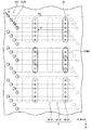
Classifications
-
- B—PERFORMING OPERATIONS; TRANSPORTING
- B41—PRINTING; LINING MACHINES; TYPEWRITERS; STAMPS
- B41J—TYPEWRITERS; SELECTIVE PRINTING MECHANISMS, i.e. MECHANISMS PRINTING OTHERWISE THAN FROM A FORME; CORRECTION OF TYPOGRAPHICAL ERRORS
- B41J2/00—Typewriters or selective printing mechanisms characterised by the printing or marking process for which they are designed
- B41J2/005—Typewriters or selective printing mechanisms characterised by the printing or marking process for which they are designed characterised by bringing liquid or particles selectively into contact with a printing material
- B41J2/01—Ink jet
- B41J2/21—Ink jet for multi-colour printing
- B41J2/2132—Print quality control characterised by dot disposition, e.g. for reducing white stripes or banding
- B41J2/2135—Alignment of dots
-
- B—PERFORMING OPERATIONS; TRANSPORTING
- B05—SPRAYING OR ATOMISING IN GENERAL; APPLYING FLUENT MATERIALS TO SURFACES, IN GENERAL
- B05D—PROCESSES FOR APPLYING FLUENT MATERIALS TO SURFACES, IN GENERAL
- B05D1/00—Processes for applying liquids or other fluent materials
- B05D1/26—Processes for applying liquids or other fluent materials performed by applying the liquid or other fluent material from an outlet device in contact with, or almost in contact with, the surface
-
- B—PERFORMING OPERATIONS; TRANSPORTING
- B05—SPRAYING OR ATOMISING IN GENERAL; APPLYING FLUENT MATERIALS TO SURFACES, IN GENERAL
- B05D—PROCESSES FOR APPLYING FLUENT MATERIALS TO SURFACES, IN GENERAL
- B05D1/00—Processes for applying liquids or other fluent materials
- B05D1/36—Successively applying liquids or other fluent materials, e.g. without intermediate treatment
-
- B—PERFORMING OPERATIONS; TRANSPORTING
- B05—SPRAYING OR ATOMISING IN GENERAL; APPLYING FLUENT MATERIALS TO SURFACES, IN GENERAL
- B05D—PROCESSES FOR APPLYING FLUENT MATERIALS TO SURFACES, IN GENERAL
- B05D3/00—Pretreatment of surfaces to which liquids or other fluent materials are to be applied; After-treatment of applied coatings, e.g. intermediate treating of an applied coating preparatory to subsequent applications of liquids or other fluent materials
- B05D3/02—Pretreatment of surfaces to which liquids or other fluent materials are to be applied; After-treatment of applied coatings, e.g. intermediate treating of an applied coating preparatory to subsequent applications of liquids or other fluent materials by baking
- B05D3/0254—After-treatment
-
- B—PERFORMING OPERATIONS; TRANSPORTING
- B41—PRINTING; LINING MACHINES; TYPEWRITERS; STAMPS
- B41J—TYPEWRITERS; SELECTIVE PRINTING MECHANISMS, i.e. MECHANISMS PRINTING OTHERWISE THAN FROM A FORME; CORRECTION OF TYPOGRAPHICAL ERRORS
- B41J25/00—Actions or mechanisms not otherwise provided for
- B41J25/001—Mechanisms for bodily moving print heads or carriages parallel to the paper surface
- B41J25/003—Mechanisms for bodily moving print heads or carriages parallel to the paper surface for changing the angle between a print element array axis and the printing line, e.g. for dot density changes
-
- H—ELECTRICITY
- H05—ELECTRIC TECHNIQUES NOT OTHERWISE PROVIDED FOR
- H05B—ELECTRIC HEATING; ELECTRIC LIGHT SOURCES NOT OTHERWISE PROVIDED FOR; CIRCUIT ARRANGEMENTS FOR ELECTRIC LIGHT SOURCES, IN GENERAL
- H05B33/00—Electroluminescent light sources
- H05B33/10—Apparatus or processes specially adapted to the manufacture of electroluminescent light sources
-
- H—ELECTRICITY
- H10—SEMICONDUCTOR DEVICES; ELECTRIC SOLID-STATE DEVICES NOT OTHERWISE PROVIDED FOR
- H10K—ORGANIC ELECTRIC SOLID-STATE DEVICES
- H10K71/00—Manufacture or treatment specially adapted for the organic devices covered by this subclass
-
- H—ELECTRICITY
- H10—SEMICONDUCTOR DEVICES; ELECTRIC SOLID-STATE DEVICES NOT OTHERWISE PROVIDED FOR
- H10K—ORGANIC ELECTRIC SOLID-STATE DEVICES
- H10K71/00—Manufacture or treatment specially adapted for the organic devices covered by this subclass
- H10K71/10—Deposition of organic active material
- H10K71/12—Deposition of organic active material using liquid deposition, e.g. spin coating
- H10K71/13—Deposition of organic active material using liquid deposition, e.g. spin coating using printing techniques, e.g. ink-jet printing or screen printing
- H10K71/135—Deposition of organic active material using liquid deposition, e.g. spin coating using printing techniques, e.g. ink-jet printing or screen printing using ink-jet printing
-
- H—ELECTRICITY
- H10—SEMICONDUCTOR DEVICES; ELECTRIC SOLID-STATE DEVICES NOT OTHERWISE PROVIDED FOR
- H10K—ORGANIC ELECTRIC SOLID-STATE DEVICES
- H10K71/00—Manufacture or treatment specially adapted for the organic devices covered by this subclass
- H10K71/10—Deposition of organic active material
- H10K71/16—Deposition of organic active material using physical vapour deposition [PVD], e.g. vacuum deposition or sputtering
- H10K71/164—Deposition of organic active material using physical vapour deposition [PVD], e.g. vacuum deposition or sputtering using vacuum deposition
Definitions
- the present invention relates to a method for manufacturing an organic EL (Electroluminescence) display panel, and particularly to a manufacturing method using a wet process.
- organic EL Electrode
- organic EL display panel a plurality of organic EL elements are arranged in a matrix along the main surface of a substrate that is a support material, and the organic EL elements constitute pixels, thereby displaying an image on the image display surface. Is done.
- the organic EL element has a structure in which a functional layer including at least a light emitting layer made of an organic compound is sandwiched between a pair of electrodes.
- the functional layer includes an injection layer, a transport layer, a blocking layer, a buffer layer, and the like.
- the formation method of the functional layer is roughly classified into a dry process such as a vacuum deposition method and a wet process such as an ink jet method.
- the wet process is a forming method using a solution (hereinafter referred to as “ink”) containing a functional layer material (functional material), and is suitable for increasing the size of a display panel from the viewpoint of the forming accuracy and cost. It is considered a technology.
- ink jet method in which ink is directly applied to a pixel formation region by ejecting ink as fine droplets onto a substrate has been progressing.
- ink is ejected from the nozzles to the pixel formation region while relatively moving a plurality of nozzles arranged in a straight line in a certain scanning direction along the main surface of the substrate.
- the scanning direction is generally set parallel to the row direction or column direction of the matrix in which the pixel formation regions are arranged.
- a technique for adjusting the coating interval between adjacent nozzles by tilting the direction in which the nozzles are arranged with respect to the scanning direction is disclosed (for example, see Patent Document 1).
- FIG. 16 is a schematic plan view showing the scanning direction dsx of the nozzle row 824 and the application location A8.
- nozzles 824N that eject ink as fine droplets are arranged in the extending direction dh.
- the pixel formation region P has subpixel formation regions SP (R), (G), and (B), and is arranged in the row direction d1 and the column direction d2.
- Each nozzle 824N moves in the scanning direction dsx parallel to the row direction d1, and is one of the sub-pixel formation regions SP (R), (G), and (B) (the sub-pixel formation region SP (B) in the drawing).
- Ink is ejected to the application location A8.
- each nozzle 824N has individual variations in the ink ejection mechanism and state variations due to changes over time, and thus individual differences may occur in the ejection amount of the droplets of the nozzle 824N.
- such individual difference in the injection amount of the nozzle 824N is reflected in the row direction d1.
- the injection amount of the hatched nozzle 824NX in FIG. 16 is extremely small (or large) compared to the injection amounts of the other nozzles 824N. Since the scanning direction dsx is parallel to the row direction d1, the sub-pixel formation region SP (B) (shaded portion in the drawing) applied by the nozzle 824NX is arranged in the row direction d1. That is, in the organic EL display panel manufactured by this method, extremely high (or low) luminance pixels, non-luminous pixels, or pixels with shifted colors are arranged in the row direction d1, and therefore, along the pixel arrangement direction. Linear brightness unevenness and color unevenness occur.
- FIG. 17 is a schematic plan view showing the scanning direction dsx of the nozzle row 924 and the application location A9.
- the extending direction dh in which the nozzles 924N are arranged is inclined with respect to the scanning direction dsx.
- the scanning direction dsx is parallel to the row direction d1, for example, the sub-pixel formation region SP applied to the nozzle 924NX having a smaller (or larger) ejection amount than the other nozzles 924N (hatched portion in the drawing).
- B shaded area in the figure
- linear luminance unevenness and color unevenness occur along the pixel arrangement direction.
- the linear luminance unevenness and color unevenness as described above do not occur only when there is an extreme individual difference in the ejection amount of the nozzle (the nozzle 824NX and the nozzle 924NX exist). Even if the individual difference is small, for example, if nozzles with individual differences of the same tendency are concentrated in a certain range, for example, the injection amount of a plurality of adjacent nozzles is less than the average, the pixel difference is superimposed due to the overlap of individual differences. Linear luminance unevenness and color unevenness occur along the direction of arrangement.
- an object of the present invention is a method of manufacturing an organic EL display panel using an ink jet method, in which generation of linear luminance unevenness and color unevenness along the pixel arrangement direction due to individual differences in nozzle injection amount is generated.
- An object of the present invention is to provide a method of manufacturing an organic EL display panel that can be reduced.
- a substrate is prepared, a plurality of first electrodes are formed on the substrate, and a partition is formed on the substrate on which the plurality of first electrodes are formed.
- a plurality of pixel formation regions arranged in a matrix surrounded by the partition walls are formed.
- the functional material is transferred from the plurality of nozzles to the plurality of pixel formation regions while relatively moving the plurality of nozzles arranged in a straight line in a certain scanning direction along the main surface of the substrate. By ejecting the contained ink, the ink is applied to each of the plurality of pixel formation regions.
- a functional layer containing a functional material is formed in each of the plurality of pixel formation regions, and a position covering the plurality of pixel formation regions where the functional layer is formed At least the second electrode is formed.
- the angle ⁇ formed between the row direction in which the plurality of pixel formation regions are arranged and the scanning direction is set to be more than 0 ° and less than 90 °, whereby each of the plurality of nozzles is set.
- the ink is applied over a plurality of rows in the pixel formation region.
- the nozzle Since the scanning direction of the nozzle is inclined with respect to the row direction, even if there is a nozzle with a smaller or larger ejection amount than other nozzles, the nozzle The pixel formation region applied by the step extends over a plurality of rows and does not line up in the row direction. Therefore, according to the manufacturing method, it is possible to reduce the occurrence of linear luminance unevenness and color unevenness along the row direction, that is, the pixel arrangement direction due to individual differences in nozzle ejection amounts.
- FIG. 1 is a block diagram illustrating an overall configuration of an organic EL display device 1.
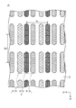
- FIG. 3 is a schematic plan view in which a part of the image display surface of the organic EL display panel 10 is enlarged.
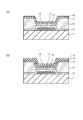
- FIG. It is a schematic cross-sectional view along the row direction d1 of the sub-pixel formation region SP.
- 5 is a process diagram for explaining a method of manufacturing the organic EL display panel 10.
- FIG. It is a schematic cross section which shows the manufacture process of the organic electroluminescent display panel 10, Comprising: (a) is a figure which shows an anode formation process, (b) is a figure which shows a positive hole injection layer formation process, (c) is It is a figure which shows a partition formation process.
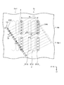
- FIG. 6 is a schematic plan view showing a scanning direction ds of the nozzle row 124 and an application location A.
- FIG. 6 is a schematic plan view illustrating scanning of the nozzle row 124 with respect to the sub-pixel formation region SP at angles ⁇ and ⁇ .
- FIG. 4 is a schematic plan view for explaining the number of scans in the inkjet apparatus 100.
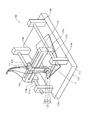
- FIG. It is a perspective view which shows the inkjet apparatus 200 which concerns on a modification.
- FIG. 10 is a schematic plan view showing a scanning direction dsx of a nozzle row 824 and an application location A8.
- FIG. 10 is a schematic plan view showing a scanning direction dsx of a nozzle row 924 and an application location A9.
- a substrate is prepared, a plurality of first electrodes are formed on the substrate, and a partition is formed on the substrate on which the plurality of first electrodes are formed.
- a plurality of pixel formation regions arranged in a matrix surrounded by the partition walls are formed.
- the functional material is transferred from the plurality of nozzles to the plurality of pixel formation regions while relatively moving the plurality of nozzles arranged in a straight line in a certain scanning direction along the main surface of the substrate. By ejecting the contained ink, the ink is applied to each of the plurality of pixel formation regions.
- a functional layer containing a functional material is formed in each of the plurality of pixel formation regions, and a position covering the plurality of pixel formation regions where the functional layer is formed At least the second electrode is formed.
- the angle ⁇ formed between the row direction in which the plurality of pixel formation regions are arranged and the scanning direction is set to be more than 0 ° and less than 90 °, whereby each of the plurality of nozzles is set.
- the ink is applied over a plurality of rows in the pixel formation region.
- the nozzle Since the scanning direction of the nozzle is inclined with respect to the row direction, even if there is a nozzle with a smaller or larger ejection amount than other nozzles, the nozzle The pixel formation region applied by the step extends over a plurality of rows and does not line up in the row direction. Therefore, according to the manufacturing method, it is possible to reduce the occurrence of linear luminance unevenness and color unevenness along the row direction, that is, the pixel arrangement direction due to individual differences in nozzle ejection amounts.
- the intervals in the matrix direction in which the plurality of pixel formation areas are arranged are constant. Further, in the manufacturing method, when the interval on the row direction side is Dp and the interval on the column direction side is Dp2 among the fixed intervals, the angle ⁇ is set so that the value of Dp ⁇ tan ⁇ is not equal to Dp2. Set.
- the interval between the plurality of nozzles is set to a constant value Dn, and the plurality of nozzles are aligned in the scanning direction.
- the angle formed by the direction is set to a constant value ⁇ .
- the angle ⁇ is set so as to satisfy the following formula 1.
- the application location of each nozzle is shifted by exactly N times the ink application interval in the pixel formation region adjacent in the row direction. Accordingly, the ink application location is preserved in any pixel formation region arranged in the row direction. As a result, the variation in the position in the column direction and the number of applications between the pixel formation regions arranged in the row direction is suppressed, and the occurrence of uneven application in the row direction is suppressed. Therefore, in the method for manufacturing the organic EL display panel according to the above aspect, it is possible to reduce the occurrence of uneven luminance and uneven coloring in the row direction.
- each of the plurality of pixel formation regions corresponds to each of red, green, and blue.
- a sub-pixel formation region is formed.
- each of the sub-pixel formation regions corresponding to red, green, and blue is scanned with a plurality of nozzles to apply different inks.
- luminance with respect to the application quantity among the said ink is more than the value of N with respect to the scanning direction at the time of apply
- the number N of nozzles to be applied is maximized and linear The occurrence of uneven brightness and color unevenness can be effectively reduced.
- the subpixel formation region when the subpixel formation region is formed, the subpixel formation region is formed in a long shape whose longitudinal direction is perpendicular to the row direction. . Furthermore, in the manufacturing method, the angle ⁇ is set to be greater than 0 ° and equal to or less than 45 ° with respect to the scanning direction when any ink is applied.
- the nozzle scanning direction is close to the row direction orthogonal to the major axis direction of the sub-pixel formation region. Therefore, in the method for manufacturing an organic EL display panel according to the above aspect, the number of application nozzles per sub-pixel formation region can be increased, and the influence due to individual differences in nozzle ejection amount can be relatively reduced.
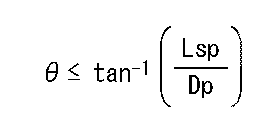
- the length in the longitudinal direction of the subpixel formation region is Lsp.
- the angle ⁇ is set so as to satisfy the following formula 2 with respect to the scanning direction when any ink is applied.
- the angle ⁇ is increased, so that the number of nozzles necessary for coating all the subpixel formation regions is increased, and the nozzle ejection amount in the column direction is increased. The reflection of individual differences can be suppressed.
- the angle ⁇ and the angle ⁇ are set so as to satisfy the following Expression 3 with respect to the scanning direction when any ink is applied. Set.
- the number of coating nozzles per sub-pixel forming region can be ensured to be equal to or higher than that of a general ink jet method, and the linear shape is obtained without increasing the luminance variation between pixels. Brightness unevenness and color unevenness can be reduced.
- the row direction and the column direction are respectively set. It is made to correspond with the longitudinal direction of a board
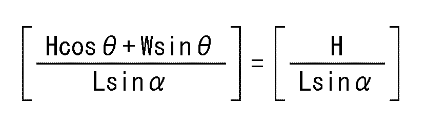
- the manufacturing method when applying ink, the length in the longitudinal direction of the substrate is W, the length in the short direction of the substrate is H, and the total length in which a plurality of nozzles are arranged is L.
- angle (theta) is set so that the following several 4 may be satisfy
- the angle formed by the two directions refers to a smaller one of the angles at which the two directions projected on the plane defined by the two directions intersect. Therefore, the angle formed by the two directions is not less than 0 ° and not more than 90 °.
- FIG. 1 is a block diagram showing the overall configuration of the organic EL display device 1.
- the organic EL display device 1 is an organic EL display device used for a television, a personal computer, a commercial display, a portable terminal, and the like, and has a rectangular organic EL display panel 10 and a drive control unit 20 connected thereto. Is provided.
- the drive control unit 20 includes four drive circuits 21 to 24 and a control circuit 25.
- the organic EL display panel 10 (hereinafter referred to as “panel 10”) is a display panel having a rectangular image display surface, and is, for example, a top emission type and active matrix type organic EL display panel.
- panel 10 is a display panel having a rectangular image display surface, and is, for example, a top emission type and active matrix type organic EL display panel.
- four drive circuits 21 to 24 are arranged around the panel 10, but the configuration of the drive control unit 20 is not limited to this, and the number and positions of the drive circuits can be changed as appropriate. It is.
- FIG. 2 is a schematic plan view in which a part of the image display surface of the panel 10 is enlarged.
- the panel 10 includes a plurality of pixel formation regions P arranged in a matrix having a row direction d1 and a column direction d2 orthogonal to each other along the image display surface.
- the intervals at which the pixel formation regions P are arranged in the row direction d1 and the column direction d2 are constant values, and the pixel formation regions P are arranged every pixel interval Dp in the row direction d1 and every pixel interval Dp2 in the column direction d2. It is out.
- each pixel formation region P one subpixel formation region SP (R), SP (G), SP (B) corresponding to each of red (R), green (G), and blue (B) is formed. And are arranged at intervals in the row direction d1.
- subpixel formation regions SP (R), SP (G), and SP (B) are not particularly distinguished, they are referred to as subpixel formation regions SP.
- the row direction d1 is parallel to the longitudinal direction of the panel 10
- the column direction d2 is parallel to the lateral direction of the panel 10.
- the transversal direction in a rectangular shape and a rectangular shape refers to the direction orthogonal to a longitudinal direction.
- FIG. 3 is a schematic cross-sectional view along the row direction d1 of the sub-pixel formation region SP.
- a top emission type organic EL element is formed in the sub-pixel formation region SP, and the first electrode 12, the transparent electrode 13, the hole injection layer 14, the partition 15, the light emitting layer 16, and the electron transport are formed on the substrate 11.
- the layer 17, the second electrode 18, and the sealing layer 19 are laminated.
- a hole transport layer, an electron injection layer, a blocking layer, a buffer layer, and the like may be stacked.
- a part of each said layer may be abbreviate
- a plurality of first electrodes 12 are formed on a substrate 11 in a matrix shape having a row direction d 1 and a column direction d 2, and a transparent electrode 13 is formed on each first electrode 12.
- a hole injection layer 14 is formed so as to cover the upper surface of the substrate 11 and all the transparent electrodes 13.
- a partition wall 15 surrounding the opening 15a for defining the pixel formation region P and the sub-pixel formation region SP is formed, and the light emitting layer 16 is formed in the opening 15a.
- the electron transport layer 17, the second electrode 18, and the sealing layer 19 are formed in this order so as to cover all the light emitting layers 16 and the partition walls 15 that are located between the light emitting layers 16.
- the said structure is an example to the last, for example, the positive hole injection layer 14, the electron carrying layer 17, or the 2nd electrode 18 may be formed only in each opening 15a.
- a plurality of first electrodes 12 may be arranged in the openings 15a of the partition walls 15 in each subpixel formation region SP in the column direction d2 of the subpixel formation region SP.
- three first electrodes 12 may be disposed in one opening 15a in the column direction d2.
- Each first electrode 12 may be controlled based on an individual signal, or the three first electrodes 12 may be controlled based on the same signal.
- a pixel regulation layer made of an electrical insulator may be provided between the first electrodes 12 in order to avoid interference from the adjacent first electrodes 12. .
- the height of the pixel restricting layer is preferably lower than the height of the partition wall 15.
- the substrate 11 is a support member for the panel 10. Although illustration is omitted, in the substrate 11, a TFT (Thin Film Transistor) layer is formed on a rectangular plate-shaped main body. In the TFT layer, a circuit for controlling a current supplied to the organic EL element is configured by electronic circuit elements such as a TFT element, a capacitor element, and a wiring. An interlayer insulating layer (not shown) is formed on the uppermost portion of the TFT layer, and the upper surface of the substrate 11 is flattened.
- TFT Thin Film Transistor
- the main body of the substrate 11 is made of an electrically insulating material.
- the material include soda glass, non-fluorescent glass, phosphate glass, borate glass, quartz, acrylic resin, styrene resin, polycarbonate resin, epoxy resin, polyethylene, polyester, and silicone. Resin, alumina or the like can be used.
- substrate 11 may coat the electrically insulating material on metal plates, such as aluminum and stainless steel, for example.
- the TFT layer of the substrate 11 includes a stacked structure of a semiconductor, a conductor, and an electrical insulator that form elements and wirings, and an interlayer insulating layer that covers the stacked structure.
- the semiconductor for example, an oxide semiconductor such as silicon or indium-zinc-gallium oxide, an organic semiconductor having a ⁇ -electron conjugated system spread in a planar direction, such as a heteroaromatic compound, or the like can be used.
- the conductor for example, a metal such as aluminum, copper, or gold, or a conductive oxide such as indium tin oxide (ITO) or indium zinc oxide (IZO) can be used.
- the insulator for example, silicon nitride, silicon oxide, silicon oxynitride, aluminum oxide, acrylic resin, polyimide resin, siloxane resin, phenol resin, or the like can be used.
- an electrically insulating patternable material for example, an organic material such as an acrylic resin, a polyimide resin, a siloxane resin, or a phenol resin can be used.
- the substrate 11 (main body) defines the longitudinal direction and the short direction of the panel 10. Therefore, the longitudinal direction of the main surface of the substrate 11 (main body) is parallel to the row direction d1, and the short side direction is parallel to the column direction d2.
- the first electrode 12 is, for example, Al (aluminum), Ag (silver), APC (alloy of silver, palladium and copper), ARA (alloy of silver, rubidium and gold), MoCr (alloy of molybdenum and chromium), Alternatively, it is made of NiCr (an alloy of nickel and chromium) and functions not only as an anode but also has a function of reflecting visible light generated in the light emitting layer 16 and guiding it upward.
- the transparent electrode 13 is made of ITO (Indium Tin Oxide), IZO (Indium Zinc Oxide) or the like, and not only functions as an anode but also is interposed between the first electrode 12 and the hole injection layer 14. It also has a function of improving the bondability of the layer.
- the hole injection layer 14 is made of, for example, a metal compound such as a metal oxide, a metal nitride, or a metal oxynitride.
- the metal oxide include Cr (chromium), Mo (molybdenum), W (tungsten), V (vanadium), Nb (niobium), Ta (tantalum), Ti (titanium), Zr (zirconium), and Hf ( Hafnium), Sc (scandium), Y (yttrium), Th (thorium), Mn (manganese), Fe (iron), Ru (ruthenium), Os (osmium), Co (cobalt), Ni (nickel), Cu ( Copper), Zn (zinc), Cd (cadmium), Al (aluminum), Ga (gallium), In (indium), Si (silicon), Ge (germanium), Sn (tin), Pb (lead), Sb ( Oxides such as antimony) and Bi (bismuth) and oxides such as so-called
- the partition wall 15 is made of, for example, an organic material such as resin or an inorganic material such as glass.
- organic materials include acrylic resins, polyimide resins, novolac-type phenol resins, and examples of inorganic materials include SiO (silicon oxide), SiN (silicon nitride), and the like.
- the partition 15 is formed so that the planar shape of the sub-pixel formation region SP (opening 15a) is substantially elliptical with the column direction d2 as the major axis and the row direction d1 as the minor axis. Yes. More specifically, the partition wall 15 surrounds the opening 15a so that two sides of the opening 15a facing the row direction d1 are linear and two sides of the opening 15a facing the column direction d2 are semicircular.
- the light emitting layer 16 is formed of, for example, F8BT (poly (9, 9-di-n-octylfluorene-alt-benzothiazole)) which is an organic polymer.
- F8BT poly (9, 9-di-n-octylfluorene-alt-benzothiazole)
- the light emitting layer 16 is not limited to the structure which consists of this material, It can be comprised so that a well-known organic material may be included.
- the electron transport layer 17 is formed of a material having a function of transporting electrons injected from the second electrode 18 to the light emitting layer 16.
- fluorenone derivatives for example, nitro-substituted fluorenone derivatives, thiopyrandioxide derivatives, difequinone derivatives, perylene tetracarboxyl derivatives, anthraquinodimethane derivatives, fluorenylidenemethane derivatives, anthrone derivatives, oxadiazole derivatives, perinone derivatives, quinoline Complex derivatives (all described in JP-A-5-163488), phosphorus oxide derivatives, triazole derivatives, todiazine derivatives, silole derivatives, dimesityl boron derivatives, triaryl boron derivatives, and the like are used.
- the second electrode 18 is made of, for example, ITO or IZO and functions as a cathode.
- the sealing layer 19 has a function of suppressing exposure of the layers below the second electrode 18 to moisture or exposure to air.
- SiN silicon nitride
- SiON silicon oxynitride
- FIG. 4 is a process diagram for explaining a manufacturing method of the panel 10.
- 5, 6, and 7 are schematic cross-sectional views illustrating the manufacturing process of the panel 10.
- the substrate 11 is prepared. Specifically, a main body in which an electrically insulating material is formed into a rectangular flat plate shape is prepared, and a TFT layer is formed on the main body.
- a method for forming the TFT layer for example, a thin film forming method such as sputtering, chemical vapor deposition, or spin coating and a patterning method such as photolithography can be combined. Further, if necessary, treatment such as plasma ion implantation and baking may be performed.
- an anode composed of the first electrode 12 and the transparent electrode 13 is formed on the substrate 11.
- the metal thin film is patterned in a matrix by, for example, photolithography to form a plurality of first electrodes 12 arranged in a matrix on the substrate 11 (FIG. 5).
- the metal thin film may be formed by vacuum deposition or the like.
- an ITO thin film is formed by, for example, sputtering, and the transparent electrode 13 is formed by patterning the ITO thin film only on the first electrode by, for example, photolithography.
- a plurality of first electrodes 12 and transparent electrodes 13 arranged in a matrix are formed on the substrate 11 by patterning the ITO thin film and the metal thin film in this order by photolithography. May be.
- the hole injection layer 14 is formed on the substrate 11 on which the transparent electrode 13 is formed. Specifically, the hole injection layer 14 is formed by forming a tungsten oxide film with a uniform film thickness over the entire upper surface side of the substrate 11 including the upper surface of the transparent electrode 13 by, for example, vacuum evaporation or sputtering. It forms (FIG.5 (b)).
- the partition wall 15 is formed on the substrate 11 on which the hole injection layer 14 is formed. Specifically, for example, a resist film containing a photoresist material is formed on the hole injection layer 14 by coating or the like, and an opening 15a is provided at a position above the transparent electrode 13 of the resist film, for example, by photolithography. A partition wall 15 is formed (FIG. 5C). At this time, the opening 15a becomes an exposed portion of the transparent electrode 13 surrounded by the partition wall 15 and arranged in a matrix. That is, the opening 15a is formed as the subpixel formation region SP. At the same time, the pixel formation region P is formed by forming the three subpixel formation regions SP arranged in the row direction d1.
- the ink 16a is applied to the substrate 11 on which the partition wall 15 is formed. Specifically, the ink 16a containing the material of the light emitting layer 16 is applied to each of the openings 15a (subpixel formation regions SP) by using an inkjet method (FIG. 6A). The details of the method of applying the ink 16a will be described later.
- Electron transport layer formation (S7) Next, the electron transport layer 17 is formed at a position covering the subpixel formation region SP where the light emitting layer 16 is formed. Specifically, for example, a thin film made of a material used for the electron transport layer is formed so as to cover the upper surface of the laminate on the substrate 11 by vacuum vapor deposition to form the electron transport layer 17 (FIG. 6C).
- a cathode composed of the second electrode 18 is formed on the substrate 11 on which the electron transport layer 17 is formed. Specifically, for example, an ITO thin film is formed so as to cover the upper surface of the laminate on the substrate 11 by sputtering to form the second electrode 18 (FIG. 7A).
- the second electrode 18 may be formed at a position that covers at least the subpixel formation region SP where the light emitting layer 16 is formed.
- the substrate 11 on which the second electrode 18 is formed is sealed.
- a silicon nitride thin film is formed so as to cover the laminate on the substrate 11 by sputtering, for example, and the sealing layer 19 is formed (FIG. 7B).
- a flat sealing material may be bonded to the upper surface side of the sealing layer 19 through an organic resin or the like.
- a color filter for correcting the emission color may be disposed on the sealing material.
- the panel 10 in which the organic EL elements are formed in each subpixel formation region SP is completed.
- the method for forming each part described above film formation method, patterning method, etc. is merely an example, and other methods may be used.
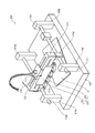
- FIG. 8 is a perspective view showing the inkjet device 100 used for applying the ink 16a.
- the ink jet apparatus 100 includes a work table 110 and a head unit 120 as main components.
- the work table 110 is a so-called gantry-type work table, and has a base 111 on which an object to be coated (the substrate 11 in this embodiment) is placed, and a long shape disposed above the base 111. And a moving gantry 112.
- the base 111 has a rectangular parallelepiped shape, and the upper surface on which the application target is placed is rectangular.
- the longitudinal direction of the base 111 is the longitudinal direction on the upper surface
- the short direction of the base 111 is the lateral direction on the upper surface.
- the movable stand 112 is bridged between a pair of guide shafts 113a and 113b arranged in parallel along the longitudinal direction of the base 111.
- the pair of guide shafts 113 a and 113 b are supported by columnar stands 114 a to 114 d disposed at the four corners of the base 111.
- Linear motor portions 115a and 115b are attached to the guide shafts 113a and 113b, respectively, so that the movable mount 112 can be moved in the longitudinal direction of the base 111.
- An L-shaped pedestal 116 is attached to the movable gantry 112, and a servo motor unit 117 is attached to the pedestal 116.
- the servo motor unit 117 can move the pedestal 116 along the guide groove 118 in the short direction of the base 111.
- the linear motor units 115a and 115b and the servo motor unit 117 are connected to a control device (not shown), and the signal from the control device moves the moving frame 112 in the longitudinal direction and the pedestal 116 in the short direction. Movement is controlled.
- the application target on the base 111 can be rotated and fixed in a plane parallel to the upper surface of the base 111, and the application target on the upper surface of the base 111 can be relative.
- the direction can be set freely.
- a rotary table or the like that can be freely rotated / fixed on the upper surface of the base 111 may be disposed at a place where the application target of the base 111 is placed.
- the head unit 120 includes a main body unit 121, an inkjet head 122, and an imaging device 123.
- the main body 121 is fixed to the pedestal 116 of the work table 110, and the inkjet head 122 and the imaging device 123 are attached to the main body 121.
- the inkjet head 122 is a long member, and although not shown, a plurality of (for example, about 10,000) nozzles 124N are arranged on a straight line in the longitudinal direction of the inkjet head 122 on the lower surface side.
- the nozzles are arranged at a constant nozzle interval Dn. Accordingly, the nozzles 124N form a nozzle row 124 in which the longitudinal direction of the inkjet head 122 is the extending direction dh.
- the nozzle 124N has a piezoelectric element (not shown) inside and a liquid chamber (not shown) connected to the piezoelectric element, and the piezoelectric element presses the liquid chamber so that the ink 16a in the liquid chamber is ejected from the nozzle 124N. Is injected from.
- the main body 121 includes a drive circuit (not shown) for individually driving the piezoelectric elements of the nozzles 124N.
- the drive circuit is connected to the aforementioned control device, and the injection amount and injection timing of each nozzle 124N are controlled by a signal from the control device.
- the main body 121 incorporates a servo motor (not shown) connected to the control device in the same manner as the drive circuit.
- the servo motor can rotate the inkjet head 122 around a main body 121 in a plane parallel to the upper surface of the base 111.
- the angle ⁇ formed between the extending direction dh of the nozzle row 124 and the longitudinal direction of the base 111 (the moving direction of the movable base 112) can be adjusted, and the relative distance of the nozzle 124N with respect to the application target, that is, the application interval can be adjusted. it can.
- the imaging device 123 is a CCD camera, for example, and is connected to the control device described above.
- the imaging device 123 images the surface of the application target and transmits the image data to the control device.
- the control apparatus can determine the presence or absence of ejection of each nozzle 124N based on the image data of the application target transmitted from the imaging apparatus 123. That is, each nozzle 124N can eject the ink 16a only to a predetermined position of the application target.
- the nozzle row 124 is attached to the pedestal 116 and the movable frame 112 via the main body 121 of the head unit 120, thereby moving the base 111 in the longitudinal direction and moving the base 111 in the short direction. Can be moved.
- the angle ⁇ formed between the extending direction dh of the nozzle row 124 and the longitudinal direction of the base 111 is set to a predetermined value. After that, the application object is placed on the base 111. Next, the relative orientation of the application object on the upper surface of the base 111 is set. Further, the base 116 is moved in the short direction of the base 111 in accordance with the angle ⁇ and the relative direction of the application target, and the range of the application target scanned by the nozzle row 124 is set.
- the nozzle 124N reaches a predetermined position on the application target while moving (scanning) the nozzle row 124 in the longitudinal direction of the base 111 by moving the movable base 112, the nozzle 124N
- the ink 16a is ejected onto the object to be coated. That is, in the ink jet apparatus 100, the longitudinal direction of the base 111 corresponds to the scanning direction ds of the nozzle row 124.
- the ink 16a is applied to a predetermined portion of the application target that the nozzle row 124 has passed.
- the nozzle row 124 is moved in the short direction of the base 111 by the movement of the base 116 after the nozzle row 124 is scanned. And the nozzle row 124 may be scanned again.
- FIG. 9 is a schematic plan view showing the scanning direction ds of the nozzle row 124 and the application location A.
- FIG. FIG. 9 shows a case where the ink 16a is applied to the sub-pixel formation area SP (B) of each pixel formation area P.
- the upper row in the drawing is the row Rm
- the lower row in the drawing is the row Rm + 1
- the right column in the drawing is the column Cn
- the left column in the drawing Is column Cn + 1.
- the relative orientation of the application object on the upper surface of the base 111 can be set in the ink jet apparatus 100 described above.
- the angle ⁇ formed by the row direction d1 in which the pixel formation regions P of the substrate 11 are arranged and the scanning direction ds of the nozzle row 124 is set to be greater than 0 ° and less than 90 °.
- the scanning direction ds has an inclination of an angle ⁇ with respect to the row direction d1, and in the figure, the nozzle row 124 moves from the upper right to the lower left of the drawing.
- Each nozzle 124N applies the ink 16a just to the center position in the row direction d1 of the sub-pixel formation region SP. Thereby, the application part A of the ink 16a is arranged in the column direction d2.
- the subpixel formation region SP to which the ink 16a is applied by the nozzle 124NX extends over a plurality of rows, and the row direction It does not line up with d1.
- the nozzle 124NX (shaded portion) passes over the sub-pixel forming region SP (B) (shaded portion) in the row Rm and enters the sub-pixel forming region SP (B). Ink 16a is applied.
- the arrival position of the nozzle 124NX is shifted downward in the column direction d2 by the angle ⁇ and is on the middle between the row Rm and the row Rm + 1. That is, the nozzle 124NX does not apply the ink 16a to the sub-pixel formation region SP (B) of the row Rm in the column Cn + 1. Therefore, the sub-pixel formation region SP (B) applied to the nozzle 124NX is aligned with the row Rm. Absent.
- the nozzle 124NX passes the upper end side of the sub-pixel formation region SP (B) in the row Rm or when the angle ⁇ is small, the nozzle 124NX also has the sub-row in the same row Rm in the column Cn + 1. There is a possibility of passing over the pixel formation region SP (B). However, in this case as well, the nozzle column 124 moves while maintaining the angle ⁇ , so that the nozzle 124NX further moves to the sub-pixel formation region SP (B) in the row Rm in the column ahead (or before the column Cn). There are rows that do not pass above.
- the total length of the rows of the pixel formation regions P arranged in the row direction d1 is very large compared to the size of the pixel formation region P, and even with a minute angle ⁇ , If tilted, the nozzle 124N will apply the ink 16a over a plurality of different rows.
- the panel 10 manufactured by the above method pixels having higher or lower luminance than the other pixels, non-light emitting pixels, or pixels whose color is shifted in the row direction d1 due to individual differences in the ejection amount of the nozzle 124N. Lined up is suppressed. Therefore, according to the manufacturing method in the present embodiment, it is possible to reduce the occurrence of linear luminance unevenness and color unevenness along the row direction d1, that is, the pixel arrangement direction, due to individual differences in nozzle ejection amounts.
- Dp ⁇ tan ⁇ is not equal to Dp2 with respect to the pixel interval Dp in the row direction d1 and the pixel interval Dp2 in the column direction d2 where the pixel formation regions P are arranged.
- Dp ⁇ tan ⁇ is equal to Dp2
- the application position in the row direction d2 of each nozzle 124N is shifted by exactly Dp2 every other row. Therefore, the combination of the nozzles 124N that apply in the pixel formation region P unit Is saved. Therefore, the pixel formation regions P in which the application amount of the ink 16a has the same tendency are arranged in the scanning direction ds, and linear luminance unevenness and color unevenness along the scanning direction ds occur.
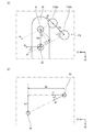
- FIG. 10A is a diagram showing the coating interval Dd1 in the sub-pixel formation region SP by the adjacent nozzles 124Na and 124Nb
- FIG. 10B is the column direction of the nozzle application locations A3 and A4 in the adjacent pixel formation region P. It is a figure which shows deviation
- N indicates the number of nozzles 124N to be applied to be replaced in the pixel formation region P adjacent in the row direction d1. Therefore, as N increases, individual variations of the nozzles 124N are less likely to be reflected in the row direction d1, and the occurrence of linear luminance unevenness and color unevenness can be further reduced.
- sub-pixel formation regions SP (R), SP (G), and SP (B) corresponding to R, G, and B are formed in the pixel formation region P, and the emission colors are different.
- a different ink 16a is applied to each.
- the inks applied to the sub-pixel formation areas SP (R), SP (G), and SP (B) are respectively the first ink 16a (R), the second ink 16a (G), and the third ink 16a (B).
- ink 16a (R), (G), (B) when describing these collectively, it describes as ink 16a (R), (G), (B).
- the nozzle row 124 is scanned for each of the sub-pixel formation regions SP (R), SP (G), and SP (B), whereby different inks 16a (R) and ( It is preferable to apply G) and (B). Thereby, different N can be set for each application of the inks 16a (R), (G), and (B).
- the scanning direction ds when applying the first ink 16a (R) is the first scanning direction ds1
- the scanning direction ds when applying the second ink 16a (G) is the second scanning direction ds2
- the third ink 16a is defined as a third scanning direction ds3.
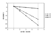
- FIG. 11 is a graph showing the relationship between the coating amount and the relative luminance in an example of the ink 16a.
- the horizontal axis and the vertical axis are relative values, the horizontal axis indicates the relative application amount of the ink 16a when a certain application amount is 1, and the vertical axis indicates the luminance with reference to a certain luminance. It shows the rate of change from luminance.
- This graph shows the relationship in an example of the inks 16a (R), (G), and (B). If different inks 16a (R), (G), and (B) are used, these graphs are used. The relationship, specifically the slope of the graph, will be different.
- the rate of change in luminance due to the change in coating amount is different.
- the luminance greatly changes depending on the application amount, but in the example of the third ink 16a (B), the luminance does not change much even if the application amount changes.
- human visual sensitivity is sensitive to a change in green, but is dull in a change in blue, and the above is considered to reflect this.
- the value of N for the second scanning direction ds2 when applying an example of the second ink 16a (G) is equal to or greater than the value of N for the first scanning direction ds1 and the value of N for the third scanning direction ds3.
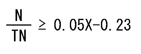
- FIG. 12 is a graph showing a relationship between coating amount variation and N / TN in an example of the ink 16a.
- the variation in the coating amount on the horizontal axis is a value determined by the ink 16a. Specifically, the difference between the average coating amount and the maximum coating amount when the same ink 16a is ejected from the nozzle 124N a plurality of times or the average coating amount. It is a percentage of a value obtained by dividing the larger of the difference from the minimum coating amount by the average coating amount.
- TN is the number of nozzles 124N that perform application per one subpixel formation region SP (hereinafter referred to as “the number of application nozzles TN”). Therefore, N / TN on the vertical axis indicates the rate of replacement of the nozzle 124N that performs coating in the pixel formation region P adjacent in the row direction d1.
- the graph of FIG. 12 a priori shows the result of the present inventor confirming the occurrence of linear luminance unevenness in the sub-pixel formation region SP of the same color using various angles ⁇ for an example of a certain ink 16a. It is the content, and shows the value of N / TN that sufficiently suppresses the occurrence of linear luminance unevenness with respect to the application amount variation in an example of the ink 16a. For example, when the result of measuring the application amount variation in one example of the first ink 16a (R) applied to the sub-pixel formation region SP (R) is 9%, N / TN is 0.22 or more. If the angle ⁇ is set, the occurrence of linear luminance unevenness is sufficiently suppressed.
- a straight line approximating this confirmation result is indicated by a broken line.
- the value of the angle ⁇ is preferably set so that N / TN is above the approximate straight line.
- the application amount variation is X%
- the following formula 5 is applied to the first scanning direction ds1 (when applying an example of the first ink 16a (R)) and the second scanning direction ds2 is applied to the second scanning direction ds2.
- the angle ⁇ is preferably set so as to satisfy the following formula 6 at the time of application of an example of the two inks 16a (G).
- N / TN (angle ⁇ ) is set to an arbitrary value with respect to the third scanning direction ds3 (during application of the third ink 16a (B)) because the change in luminance due to variation in the application amount is small. It doesn't matter.
- the opening 15a that is, the sub-pixel formation region SP is formed in a long shape so that the longitudinal direction thereof is orthogonal to the row direction d1.
- the sub-pixel formation region SP is formed in a substantially elliptical shape with the major axis direction as the column direction d2 and the minor axis direction as the row direction d1.
- the scanning direction ds (first scanning direction ds1, second scanning direction ds2, and third scanning direction ds3) of the nozzle row 124 is greater than the major axis direction d2 of the sub-pixel formation region SP. Is preferably closer to the minor axis direction d1.
- the angle formed by the scanning direction ds of the nozzle row 124 and the minor axis direction d1 of the sub-pixel formation region SP that is, the angle ⁇ to be greater than 0 ° and 45 ° or less.
- the angle ⁇ is set so as to satisfy the following formula 2 when the length in the longitudinal direction of the sub-pixel formation region SP is Lsp. It is preferable to do.
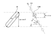
- FIG. 13 is a schematic plan view illustrating scanning of the sub-pixel formation region SP of the nozzle row 124 at angles ⁇ and ⁇ .
- the number TN of application nozzles is [(Lsp ⁇ cos ⁇ ) / (Dn ⁇ sin ⁇ )] or [(Lsp ⁇ cos ⁇ ) / (Dn ⁇ sin ⁇ )] + 1.
- the symbol indicated by [] is a so-called Gaussian symbol, and [A] is the maximum integer not exceeding A. Therefore, A is not less than [A] and less than [A] +1.
- N is the number of nozzles 124N to be replaced in the pixel formation region P adjacent in the row direction d1.
- N is preferably equal to or less than TN, that is, the angle ⁇ preferably satisfies Equation 2.
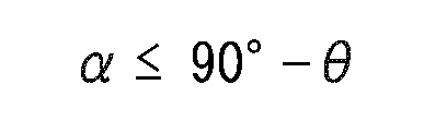
- the angle ⁇ is an angle formed by the scanning direction ds and the extending direction dh of the nozzle row 124, and is a parameter for adjusting the coating interval Dd1.
- the angle ⁇ is preferably set so as to satisfy the following formula 3 with respect to the angle ⁇ .
- the number TN of application nozzles satisfies the following inequality (7).
- FIG. 14 is a schematic plan view for explaining the number of scans in the ink jet apparatus 100.
- the inkjet head 122 on the right side of the paper moves in the scanning direction ds and applies the ink 16 a onto the substrate 11.
- the minimum number of scans required to apply the ink 16a to the entire surface of the substrate 11 is the value +1 on the left side of Equation 4.
- the minimum number of scans is the value on the right side of Equation 6 + 1. Therefore, when Expression 4 is satisfied, the ink 16a can be applied to the entire surface of the substrate 11 without increasing the number of scans compared to a general ink jet method, and an increase in manufacturing steps can be suppressed.
- the difference between the size of the image display surface of the substrate 11 and the size of the pixel arrangement region is very small (not considering the so-called frame portion), and the length in the longitudinal direction of the ink jet head 122; The difference from the total length L of the nozzle row 124 is ignored as it is minute.
- FIG. 15 is a perspective view showing an inkjet apparatus 200 according to a modification.
- a configuration in which a plurality of inkjet heads 222 are attached to the head unit 220 and the nozzles 124N are arranged in a straight line in each inkjet head 222 may be used as in the inkjet device 200. That is, the straight line in which the nozzles 124N are arranged may be plural as long as the directions are parallel.
- the setting of the angle ⁇ between the row direction d1 in which the sub-pixel formation regions SP are arranged and the scanning direction ds is set by the rotation of the substrate 11 on the base 111. It is not limited to this.
- the scanning direction ds may be set by fixing the substrate 11 to the base 111 while allowing the guide shafts 113 a and 113 b to rotate in a plane parallel to the upper surface of the base 111.
- the nozzle 124N is moved in the scanning direction ds.
- the present invention is not limited to this, and the nozzle 124N is relatively moved by moving the substrate 11 in the direction opposite to the scanning direction ds. May be moved in the scanning direction ds.
- the angle ⁇ is the angle formed between the scanning direction ds of the nozzle row 124 and the row direction d1 in which the pixel formation regions P are arranged. It may be considered as an angle formed by the scanning direction ds and the column direction d2 in which the pixel formation regions P are arranged.
- the ink jet method is used to form the light emitting layer 16, but the ink jet method may be used to form a functional layer other than the light emitting layer 16 (for example, the electron transport layer 17).
- the coating amount (layer thickness) in the formation of the functional layer other than the light emitting layer 16 also affects the luminance of the pixel. Therefore, also in this case, the angle formed by the row direction d1 and the scanning direction ds exceeds 0 °. By setting the angle to less than 90 °, it is possible to reduce the occurrence of linear luminance unevenness and color unevenness in the row direction d1.
- the matrix direction (row direction d1 and column direction d2) in which the pixel formation regions P are arranged is parallel to the longitudinal direction and the short direction of the main surface of the substrate 11.
- the row direction d1 or the column direction d2 or both directions may be directions that are neither parallel nor orthogonal to the longitudinal direction and the short direction of the substrate 11.
- the row direction d1 and the column direction d2 are not limited to an orthogonal relationship.
- the scanning direction ds can be inclined (angle ⁇ ) with respect to both the row direction d1 and the column direction d2, thereby reducing the occurrence of linear luminance unevenness and color unevenness in both directions of the matrix. That is, there is essentially no distinction between the row direction d1 and the column direction d2, and there is no problem even if they are interchanged (the column direction d2 is referred to as the “row direction”).
- the sub-pixel formation areas SP of three colors of red, green, and blue are formed in the pixel formation area P.
- the sub-pixel formation area SP may be, for example, one red color.
- four colors of red, green, blue and yellow may be used.
- the sub-pixel formation region SP is not limited to one per color in the pixel formation region P, and a plurality of sub-pixel formation regions SP may be formed.
- the arrangement of the sub-pixel formation regions SP is not limited to the configuration aligned in the row direction d1, and may be, for example, a configuration aligned in the column direction d2 or a configuration aligned in the shape of a triangular vertex. Note that when there is one sub-pixel formation region SP per pixel formation region P, all portions described as the sub-pixel formation region SP can be read as the pixel formation region P in this embodiment.
- the main body of the substrate 11 (a portion excluding the TFT layer) is rectangular, but is not limited thereto, and may be a polygon other than a square or a rectangle, a circle, an ellipse, or the like.
- the first electrode 12 is an anode and the second electrode 18 is a cathode.
- the present invention is not limited to this, and an inverted structure may be used in which the first electrode 12 is a cathode and the second electrode is an anode.
- the partition wall 15 of the panel 10 may be configured to surround the periphery of each subpixel formation region SP (pixel bank method), for example, to surround the periphery of each subpixel formation region SP arranged in the column direction d2. It may be configured (line bank method).
- line bank method an obstacle (pixel restriction layer) is formed to prevent crosstalk between the sub-pixel formation regions SP adjacent in the normal column direction d2. Therefore, even in the above-described line bank method, the fluidity of the ink in the column direction d2 is limited due to the obstacle, and it is possible to suppress the individual difference in the ejection amount of the nozzle 124N from being reflected in the row direction d1.
- the manufacturing method of the present embodiment is useful.
- the panel 10 is a top emission type and active matrix type organic EL display panel, but is not limited to this.
- a bottom emission type or passive matrix type may be adopted.
- the method for producing an organic EL display panel according to the present invention can be widely used as a method for producing a display panel used in various electronic devices such as a television, a personal computer, a commercial display, and a portable terminal.
Landscapes
- Engineering & Computer Science (AREA)
- Manufacturing & Machinery (AREA)
- Quality & Reliability (AREA)
- Electroluminescent Light Sources (AREA)
- Application Of Or Painting With Fluid Materials (AREA)
Abstract
Description
本発明の一態様に係る有機EL表示パネルの製造方法では、基板を準備し、基板上に複数の第1電極を形成し、複数の第1電極が形成された基板上に隔壁を形成して、隔壁が囲む行列状に並んだ複数の画素形成領域を形成する。また、当該製造方法では、直線上に並んだ複数のノズルを、基板の主面に沿った一定の走査方向に相対的に移動させながら、複数のノズルから複数の画素形成領域へ機能性材料を含有するインクを噴射することにより、複数の画素形成領域の各々に対してインクを塗布する。さらに、当該製造方法では、塗布されたインクを乾燥することにより、複数の画素形成領域の各々に機能性材料を含む機能層を形成し、機能層が形成された複数の画素形成領域を覆う位置に少なくとも第2電極を形成する。そして、当該製造方法では、インクを塗布する際に、複数の画素形成領域が並ぶ行方向と走査方向とのなす角度θを0°超90°未満に設定することにより、複数のノズルの各々が、画素形成領域の複数の行に渡って、前記インクを塗布する。


以下では、本発明の一態様に係る有機EL表示パネルの製造方法について、図面を参照しながら説明する。
図1は、有機EL表示装置1の全体構成を示すブロック図である。有機EL表示装置1は、テレビ、パーソナルコンピュータ、業務用ディスプレイ、携帯端末などに用いられる有機EL表示装置であって、長方形状の有機EL表示パネル10と、これに接続された駆動制御部20とを備える。駆動制御部20は、4つの駆動回路21~24と制御回路25とから構成されている。
図2は、パネル10の画像表示面の一部を拡大した模式平面図である。パネル10は、画像表示面に沿って直交する行方向d1及び列方向d2からなる行列状に並んだ複数の画素形成領域Pを備える。画素形成領域Pが行方向d1及び列方向d2に並ぶ間隔は一定の値であり、行方向d1においては画素間隔Dpごとに、列方向d2においては画素間隔Dp2ごとに、画素形成領域Pが並んでいる。
図4は、パネル10の製造方法を説明するための工程図である。図5、図6、図7はパネル10の製造過程を示す模式断面図である。
まず、基板11を準備する。具体的には、電気絶縁性材料を長方形平板状に成形した本体を用意し、本体上にTFT層を形成する。TFT層の形成方法としては、例えば、スパッタリング、化学蒸着、スピンコートなどの薄膜形成法と、フォトリソグラフィなどのパターニング法を組み合わせることができる。また、必要に応じてプラズマ・イオン注入、ベーキングなどの処理を行ってもよい。
次に、基板11上に、第1電極12及び透明電極13からなる陽極を形成する。具体的には、例えばスパッタリングにより金属薄膜を形成した後に、当該金属薄膜を例えばフォトリソグラフィで行列状にパターニングすることにより基板11上に行列状に並ぶ複数の第1電極12を形成する(図5(a))。なお、金属薄膜は真空蒸着などで形成しても良い。同様に、例えばスパッタリングによりITO薄膜を形成し、当該ITO薄膜を例えばフォトリソグラフィにより第1電極上にのみパターニングすることにより透明電極13を形成する。また、上記において、金属薄膜及びITO薄膜を形成後、フォトリソグラフィにより、ITO薄膜、金属薄膜の順にパターニングすることにより、基板11上に行列状に並ぶ複数の第1電極12及び透明電極13を形成してもよい。
次に、透明電極13が形成された基板11上に正孔注入層14を形成する。具体的には、例えば真空蒸着法又はスパッタリングなどにより透明電極13の上面を含む基板11の上面側全体に亘って均一な膜厚で酸化タングステン膜を成膜することにより、正孔注入層14を形成する(図5(b))。
次に、正孔注入層14が形成された基板11上に隔壁15を形成する。具体的には、例えば、正孔注入層14上に塗布などによりフォトレジスト材料を含むレジスト膜を形成し、当該レジスト膜の透明電極13の上方にあたる位置に、例えばフォトリソグラフィにより開口15aを設け、隔壁15を形成する(図5(c))。このとき、開口15aは、隔壁15に囲まれ、かつ行列状に並んだ透明電極13の露出部となる。すなわち、副画素形成領域SPとして開口15aが形成される。また、同時に、行方向d1に並ぶ3つの副画素形成領域SPが形成されることによって、画素形成領域Pが形成される。
次に、隔壁15が形成された基板11にインク16aを塗布する。具体的には、インクジェット法を用いて、開口15a(副画素形成領域SP)の各々に対して、発光層16の材料を含有するインク16aを塗布する(図6(a))。なお、インク16aの塗布方法の詳細については後述する。
次に、塗布されたインク16aを乾燥する。具体的には、インク16a塗布後の基板11を真空チャンバーなどの真空環境に置くことによって、インク16aの溶媒を蒸発させて乾燥する。これにより、副画素形成領域SPの各々に発光層16を形成する(図6(b))。
次に、発光層16が形成された副画素形成領域SPを覆う位置に電子輸送層17を形成する。具体的には、例えば真空蒸着により基板11上の積層物の上面を覆うように電子輸送層に用いる材料からなる薄膜を成膜して電子輸送層17を形成する(図6(c))。
次に、電子輸送層17が形成された基板11上に第2電極18からなる陰極を形成する。具体的には、例えばスパッタリングにより基板11上の積層物の上面を覆うようにITO薄膜を成膜して第2電極18を形成する(図7(a))。なお、第2電極18は、少なくとも発光層16が形成された副画素形成領域SPを覆う位置に形成されればよい。
最後に、第2電極18を形成した基板11を封止する。具体的には、例えばスパッタリング法により基板11上の積層物を覆うように窒化シリコン薄膜を成膜して封止層19を形成する(図7(b))。なお、封止層19の形成後、有機樹脂などを介して平板状の封止材を封止層19の上面側に貼り合わせてもよい。また、当該封止材には発光色を補正するカラーフィルタなどを配置してもよい。
以下、パネル10の製造方法における、インクジェット法を用いたインク16aの塗布方法について説明する。
図8は、インク16aの塗布に用いるインクジェット装置100を示す斜視図である。インクジェット装置100は、主要な構成要素として、作業テーブル110、ヘッド部120を備える。
作業テーブル110は、いわゆるガントリー式の作業テーブルであって、塗布対象物(本実施の形態では基板11)が載置される基台111と、基台111の上方に配置された長尺状の移動架台112とを備える。
ヘッド部120は、本体部121、インクジェットヘッド122及び撮像装置123を備える。本体部121は、作業テーブル110の台座116に固定され、インクジェットヘッド122と撮像装置123は、本体部121に取り付けられている。
インクジェット装置100を用いたインク16aの塗布においては、例えば、まずノズル列124の延伸方向dhと基台111の長手方向とのなす角度αを所定の値に設定した後に、基台111上に塗布対象物を載置する。次に、基台111の上面における塗布対象物の相対的な向きを設定する。さらに、上記角度α及び塗布対象物の相対的な向きに応じ、台座116を基台111の短手方向に移動させ、ノズル列124が走査する塗布対象物の範囲を設定する。
以下に、インクジェット装置100を用いた基板11へのインク16aの塗布方法について説明する。
(1)角度θの好適値
パネル10の製造方法においては、角度θが0°超90°未満であれば、特定の値に限定されず、上記効果を有する。一方で、角度θを一定の値に設定することで、さらなる効果を付加することが可能である。
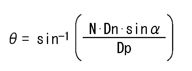
上記のように、角度θが数1を満たすとき、行方向d1に隣接する画素形成領域Pでは、ノズル124Nの塗布箇所Aが列方向d2にN・Dd1だけずれる。すなわち、Nは、行方向d1に隣接する画素形成領域Pにおいて、塗布を行うノズル124Nの入れ替わる数を示している。したがって、Nが大きいほど、ノズル124Nの個体ばらつきが行方向d1に反映されにくくなり、線状の輝度むらや発色むらの発生をより低減できる。

パネル10では、開口15aすなわち副画素形成領域SPは、その長手方向が行方向d1と直交するように長尺状に形成されている。具体的には、図2に示すように、副画素形成領域SPは、長軸方向を列方向d2、短軸方向を行方向d1とする略楕円状に形成されている。
副画素形成領域SPへのインク16aの塗布においては、副画素形成領域SPの長手方向の長さをLspとするとき、下記数2を満たすように、角度θを設定することが好ましい。

角度αは、走査方向dsとノズル列124の延伸方向dhとのなす角であり、塗布間隔Dd1を調整するパラメータである。この角度αは、角度θに対して下記数3を満たすように設定することが好ましい。

副画素形成領域SPへのインク16aの塗布においては、基板11の長手方向の長さをW、短手方向の長さをH、ノズル列124の延伸方向dhの全長をLとするとき、下記数4を満たすように角度θを設定することが好ましい。

本願においては、数1から数7の数式を示したが、これらにおける等号は厳密なものを要求する訳ではなく、現実的な範囲で一致していれば、等号が成立するとみなしてもよい。例えば、左辺と右辺の比較において、有効数字の上位2桁が一致していれば、左辺と右辺んとの等号が成立するとみなしてもよい。
11 基板
12 第1電極
15 隔壁
16 発光層(機能層)
16a インク
18 第2電極
124N、824N、924N ノズル
Dp、Dp2 画素間隔
Dn ノズル間隔
Lsp 長さ
N 正の整数
P 画素形成領域
SP 副画素形成領域
d1 行方向
d2 列方向
ds、dsx 走査方向
α、θ 角度
Claims (8)
- 基板を準備し、
前記基板上に複数の第1電極を形成し、
前記複数の第1電極が形成された前記基板上に隔壁を形成して、前記隔壁が囲む行列状に並んだ複数の画素形成領域を形成し、
直線上に並んだ複数のノズルを、前記基板の主面に沿った一定の走査方向に相対的に移動させながら、前記複数のノズルから前記複数の画素形成領域へ機能性材料を含有するインクを噴射することにより、前記複数の画素形成領域の各々に対して前記インクを塗布し、
塗布された前記インクを乾燥することにより、前記複数の画素形成領域の各々に前記機能性材料を含む機能層を形成し、
前記機能層が形成された前記複数の画素形成領域を覆う位置に少なくとも第2電極を形成し、
前記インクを塗布する際に、前記複数の画素形成領域が並ぶ行方向と前記走査方向とのなす角度θを0°超90°未満に設定することにより、前記複数のノズルの各々が、前記複数の画素形成領域の複数の行に渡って、前記インクを塗布する、
有機EL表示パネルの製造方法。 - 前記複数の画素形成領域を形成する際に、前記複数の画素形成領域が並ぶ行列方向の間隔を一定とし、当該一定の間隔のうち、前記行方向側の間隔をDp、列方向側の間隔をDp2とするとき、Dp×tanθの値が、Dp2と等しくならないように、前記角度θを設定する、
請求項1に記載の有機EL表示パネルの製造方法。 - 前記インクを塗布する際に、前記複数のノズルが並ぶ間隔を一定の値Dnに、前記走査方向と前記複数のノズルが並ぶ方向とのなす角度を一定の値αに、それぞれ設定し、Nを正の整数とするとき、下記数1を満たすように、前記角度θを設定する、
請求項2に記載の有機EL表示パネルの製造方法。

- 前記複数の画素形成領域を形成する際、前記複数の画素形成領域の各々に赤色、緑色及び青色のそれぞれに対応する副画素形成領域を形成し、
前記インクを塗布する際に、赤色、緑色、青色に対応する前記副画素形成領域ごとに対して、前記複数のノズルの走査を行うことにより、それぞれ異なる前記インクを塗布し、
前記インクのうち、塗布量に対する輝度の変化が最も大きな前記インクを塗布する際の前記走査方向に対する前記Nの値が、他の前記インクを塗布する際の前記走査方向に対する前記Nの値以上となるように、前記角度θを設定する、
請求項3に記載の有機EL表示パネルの製造方法。 - 前記副画素形成領域を形成する際、長手方向が前記行方向と直交する長尺状に前記副画素形成領域を形成し、
いずれの前記インクを塗布する際の前記走査方向に対しても、前記角度θを0°超45°以下に設定する、
請求項4に記載の有機EL表示パネルの製造方法。 - 前記副画素形成領域の長手方向の長さをLspとするとき、
いずれの前記インクを塗布する際の前記走査方向に対しても、下記数2を満たすように、前記角度θを設定する、
請求項5に記載の有機EL表示パネルの製造方法。
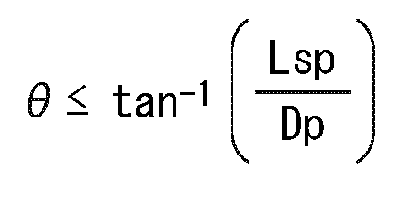
- いずれの前記インクを塗布する際の前記走査方向に対しても、下記数3を満たすように、前記角度θ及び前記角度αを設定する、
請求項6に記載の有機EL表示パネルの製造方法。

- 主面が長方形状である前記基板を準備し、
前記画素形成領域を形成する際、前記行方向、前記列方向を、それぞれ前記基板の長手方向、短手方向と一致させ、
前記インクを塗布する際に、前記基板の長手方向の長さをW、前記基板の短手方向の長さをH、前記複数のノズルが並ぶ全長をLとするとき、いずれの前記インクを塗布する際の前記走査方向に対しても、下記数4を満たすよう前記角度θを設定する、
請求項7に記載の有機EL表示パネルの製造方法。

Priority Applications (3)
| Application Number | Priority Date | Filing Date | Title |
|---|---|---|---|
| JP2016512589A JP6336044B2 (ja) | 2014-04-10 | 2015-03-27 | 有機el表示パネルの製造方法 |
| US15/302,900 US10541367B2 (en) | 2014-04-10 | 2015-03-27 | Organic EL display panel production method |
| CN201580018620.0A CN106165542B (zh) | 2014-04-10 | 2015-03-27 | 有机el显示面板的制造方法 |
Applications Claiming Priority (2)
| Application Number | Priority Date | Filing Date | Title |
|---|---|---|---|
| JP2014081099 | 2014-04-10 | ||
| JP2014-081099 | 2014-04-10 |
Publications (1)
| Publication Number | Publication Date |
|---|---|
| WO2015155953A1 true WO2015155953A1 (ja) | 2015-10-15 |
Family
ID=54287542
Family Applications (1)
| Application Number | Title | Priority Date | Filing Date |
|---|---|---|---|
| PCT/JP2015/001781 Ceased WO2015155953A1 (ja) | 2014-04-10 | 2015-03-27 | 有機el表示パネルの製造方法 |
Country Status (4)
| Country | Link |
|---|---|
| US (1) | US10541367B2 (ja) |
| JP (1) | JP6336044B2 (ja) |
| CN (1) | CN106165542B (ja) |
| WO (1) | WO2015155953A1 (ja) |
Cited By (1)
| Publication number | Priority date | Publication date | Assignee | Title |
|---|---|---|---|---|
| WO2021079417A1 (ja) * | 2019-10-21 | 2021-04-29 | シャープ株式会社 | 発光デバイス及び発光デバイスの製造方法 |
Families Citing this family (5)
| Publication number | Priority date | Publication date | Assignee | Title |
|---|---|---|---|---|
| KR102400483B1 (ko) * | 2015-10-02 | 2022-05-23 | 삼성디스플레이 주식회사 | 유기 발광 디스플레이 장치용 제조 장치와, 이를 이용한 유기 발광 디스플레이 장치의 제조 방법 |
| CN110421969B (zh) * | 2018-09-19 | 2021-02-12 | 广东聚华印刷显示技术有限公司 | 墨水填充元件载具及其控制方法、装置和计算机设备 |
| JP7257032B2 (ja) * | 2019-02-08 | 2023-04-13 | 株式会社Joled | 有機el表示パネル及び有機el表示パネルの製造方法 |
| US11474372B2 (en) * | 2020-07-22 | 2022-10-18 | Samsung Electronics Company, Ltd. | Laterally offset parallax barriers in multi-view display |
| CN111754918B (zh) * | 2020-07-30 | 2023-09-29 | 京东方科技集团股份有限公司 | 圆形显示面板的扫描修正方法及显示装置 |
Citations (4)
| Publication number | Priority date | Publication date | Assignee | Title |
|---|---|---|---|---|
| JP2005296854A (ja) * | 2004-04-13 | 2005-10-27 | Sharp Corp | 膜形成装置及び膜形成方法 |
| JP2006159703A (ja) * | 2004-12-08 | 2006-06-22 | Seiko Epson Corp | 液滴吐出装置を用いた描画方法、液滴吐出装置、並びに電気光学装置の製造方法、電気光学装置、および電子機器 |
| JP2010005619A (ja) * | 2005-04-28 | 2010-01-14 | Shibaura Mechatronics Corp | 溶液の塗布装置及び塗布方法 |
| JP2010266636A (ja) * | 2009-05-14 | 2010-11-25 | Seiko Epson Corp | カラーフィルタ基板の製造方法及びカラーフィルタの製造方法並びにカラーフィルタ基板 |
Family Cites Families (12)
| Publication number | Priority date | Publication date | Assignee | Title |
|---|---|---|---|---|
| US4219822A (en) * | 1978-08-17 | 1980-08-26 | The Mead Corporation | Skewed ink jet printer with overlapping print lines |
| JPH05163488A (ja) | 1991-12-17 | 1993-06-29 | Konica Corp | 有機薄膜エレクトロルミネッセンス素子 |
| US5443922A (en) | 1991-11-07 | 1995-08-22 | Konica Corporation | Organic thin film electroluminescence element |
| WO1998002530A1 (en) * | 1996-07-15 | 1998-01-22 | The Government Of The United States Of America, As Represented By The Department Of Health And Human Services | Production of attenuated respiratory syncytial virus vaccines from cloned nucleotide sequences |
| GB9808806D0 (en) | 1998-04-24 | 1998-06-24 | Cambridge Display Tech Ltd | Selective deposition of polymer films |
| US6736484B2 (en) * | 2001-12-14 | 2004-05-18 | Seiko Epson Corporation | Liquid drop discharge method and discharge device; electro optical device, method of manufacture thereof, and device for manufacture thereof; color filter method of manufacture thereof, and device for manufacturing thereof; and device incorporating backing, method of manufacturing thereof, and device for manufacture thereof |
| US6921148B2 (en) * | 2002-01-30 | 2005-07-26 | Seiko Epson Corporation | Liquid drop discharge head, discharge method and discharge device; electro optical device, method of manufacture thereof, and device for manufacture thereof; color filter, method of manufacture thereof, and device for manufacture thereof; and device incorporating backing, method of manufacture thereof, and device for manufacture thereof |
| JP2004111074A (ja) | 2002-09-13 | 2004-04-08 | Toshiba Corp | 有機el表示装置の製造装置と、その製造方法 |
| US7132788B2 (en) * | 2003-09-09 | 2006-11-07 | Osram Opto Semiconductors Gmbh | Optimal bank shapes for inkjet printing |
| KR20060106288A (ko) * | 2005-04-07 | 2006-10-12 | 삼성전자주식회사 | 롤 브러싱 장치, 이를 포함하는 잉크젯 헤드 클리닝 시스템및 그 방법 |
| JP5543600B2 (ja) | 2010-08-06 | 2014-07-09 | パナソニック株式会社 | 発光素子、発光素子を備えた発光装置および発光素子の製造方法 |
| CN102742357A (zh) * | 2010-08-06 | 2012-10-17 | 松下电器产业株式会社 | 有机el显示面板、显示装置以及有机el显示面板的制造方法 |
-
2015
- 2015-03-27 CN CN201580018620.0A patent/CN106165542B/zh active Active
- 2015-03-27 WO PCT/JP2015/001781 patent/WO2015155953A1/ja not_active Ceased
- 2015-03-27 US US15/302,900 patent/US10541367B2/en active Active
- 2015-03-27 JP JP2016512589A patent/JP6336044B2/ja active Active
Patent Citations (4)
| Publication number | Priority date | Publication date | Assignee | Title |
|---|---|---|---|---|
| JP2005296854A (ja) * | 2004-04-13 | 2005-10-27 | Sharp Corp | 膜形成装置及び膜形成方法 |
| JP2006159703A (ja) * | 2004-12-08 | 2006-06-22 | Seiko Epson Corp | 液滴吐出装置を用いた描画方法、液滴吐出装置、並びに電気光学装置の製造方法、電気光学装置、および電子機器 |
| JP2010005619A (ja) * | 2005-04-28 | 2010-01-14 | Shibaura Mechatronics Corp | 溶液の塗布装置及び塗布方法 |
| JP2010266636A (ja) * | 2009-05-14 | 2010-11-25 | Seiko Epson Corp | カラーフィルタ基板の製造方法及びカラーフィルタの製造方法並びにカラーフィルタ基板 |
Cited By (2)
| Publication number | Priority date | Publication date | Assignee | Title |
|---|---|---|---|---|
| WO2021079417A1 (ja) * | 2019-10-21 | 2021-04-29 | シャープ株式会社 | 発光デバイス及び発光デバイスの製造方法 |
| US12274144B2 (en) | 2019-10-21 | 2025-04-08 | Sharp Kabushiki Kaisha | Light-emitting device and method of manufacturing light-emitting device capable of restraining the expansion of dark spots |
Also Published As
| Publication number | Publication date |
|---|---|
| JP6336044B2 (ja) | 2018-06-06 |
| US10541367B2 (en) | 2020-01-21 |
| CN106165542A (zh) | 2016-11-23 |
| US20170033288A1 (en) | 2017-02-02 |
| JPWO2015155953A1 (ja) | 2017-04-13 |
| CN106165542B (zh) | 2018-08-07 |
Similar Documents
| Publication | Publication Date | Title |
|---|---|---|
| US9082732B2 (en) | Organic EL display panel and method for manufacturing same | |
| JP6594863B2 (ja) | 有機el表示パネル及び有機el表示装置 | |
| JP6336044B2 (ja) | 有機el表示パネルの製造方法 | |
| JP6387580B2 (ja) | 有機el表示パネルの製造方法 | |
| CN108417600B (zh) | 有机el显示面板以及有机el显示面板的制造方法 | |
| JP5543597B2 (ja) | 有機el表示パネルの製造方法 | |
| CN111863881B (zh) | Oled显示装置及制造oled显示装置的方法 | |
| JP6199967B2 (ja) | 有機エレクトロルミネッセンス素子の製造方法 | |
| US10879327B2 (en) | Organic EL display panel and method of manufacturing the same, organic EL display device and electronic apparatus | |
| US20210343968A1 (en) | Method of manufacturing an organic el element | |
| CN112635524A (zh) | 自发光型显示面板 | |
| JP2020030933A (ja) | 有機el表示パネル、及び有機el表示パネルの製造方法 | |
| JP2019125501A (ja) | 有機el表示パネル及びその製造方法 | |
| JP2018133242A (ja) | 有機el表示パネル、及び有機el表示パネルの製造方法 | |
| JP5313406B2 (ja) | 被成膜基板、有機el表示装置 | |
| JP6057052B2 (ja) | 表示素子、及び表示素子の製造方法 | |
| JP5899531B2 (ja) | 有機el素子の製造方法 | |
| JP2012252983A (ja) | 有機el表示パネルの製造方法、カラーフィルターの製造方法、有機el表示パネルの製造装置および有機el表示パネル | |
| JP2015207527A (ja) | 有機発光デバイスの機能層の形成方法及び有機発光デバイスの製造方法 | |
| JP6083589B2 (ja) | インクジェット装置および有機el表示パネルの製造方法 | |
| JP2018092788A (ja) | 有機el表示パネルの製造方法、有機el表示パネル製造用基板、及び有機el表示パネルの製造におけるノズルの検査方法 | |
| JP2021140885A (ja) | 表示パネル及びその製造方法 | |
| JP2018125092A (ja) | 機能層の形成方法、及び機能層形成用基板 | |
| JP2020113529A (ja) | 有機el表示パネル、及び有機el表示パネルの製造方法 |
Legal Events
| Date | Code | Title | Description |
|---|---|---|---|
| 121 | Ep: the epo has been informed by wipo that ep was designated in this application |
Ref document number: 15777125 Country of ref document: EP Kind code of ref document: A1 |
|
| ENP | Entry into the national phase |
Ref document number: 2016512589 Country of ref document: JP Kind code of ref document: A |
|
| WWE | Wipo information: entry into national phase |
Ref document number: 15302900 Country of ref document: US |
|
| NENP | Non-entry into the national phase |
Ref country code: DE |
|
| 122 | Ep: pct application non-entry in european phase |
Ref document number: 15777125 Country of ref document: EP Kind code of ref document: A1 |