WO2015125793A1 - 突入電流抑制回路 - Google Patents
突入電流抑制回路 Download PDFInfo
- Publication number
- WO2015125793A1 WO2015125793A1 PCT/JP2015/054346 JP2015054346W WO2015125793A1 WO 2015125793 A1 WO2015125793 A1 WO 2015125793A1 JP 2015054346 W JP2015054346 W JP 2015054346W WO 2015125793 A1 WO2015125793 A1 WO 2015125793A1
- Authority
- WO
- WIPO (PCT)
- Prior art keywords
- inductor
- inrush current
- current
- fet
- suppression circuit
- Prior art date
- Legal status (The legal status is an assumption and is not a legal conclusion. Google has not performed a legal analysis and makes no representation as to the accuracy of the status listed.)
- Ceased
Links
Images


Classifications
-
- H—ELECTRICITY
- H02—GENERATION; CONVERSION OR DISTRIBUTION OF ELECTRIC POWER
- H02H—EMERGENCY PROTECTIVE CIRCUIT ARRANGEMENTS
- H02H9/00—Emergency protective circuit arrangements for limiting excess current or voltage without disconnection
- H02H9/001—Emergency protective circuit arrangements for limiting excess current or voltage without disconnection limiting speed of change of electric quantities, e.g. soft switching on or off
-
- H—ELECTRICITY
- H02—GENERATION; CONVERSION OR DISTRIBUTION OF ELECTRIC POWER
- H02H—EMERGENCY PROTECTIVE CIRCUIT ARRANGEMENTS
- H02H9/00—Emergency protective circuit arrangements for limiting excess current or voltage without disconnection
- H02H9/02—Emergency protective circuit arrangements for limiting excess current or voltage without disconnection responsive to excess current
- H02H9/025—Current limitation using field effect transistors
-
- H—ELECTRICITY
- H02—GENERATION; CONVERSION OR DISTRIBUTION OF ELECTRIC POWER
- H02J—CIRCUIT ARRANGEMENTS OR SYSTEMS FOR SUPPLYING OR DISTRIBUTING ELECTRIC POWER; SYSTEMS FOR STORING ELECTRIC ENERGY
- H02J1/00—Circuit arrangements for DC mains or DC distribution networks
-
- H—ELECTRICITY
- H02—GENERATION; CONVERSION OR DISTRIBUTION OF ELECTRIC POWER
- H02J—CIRCUIT ARRANGEMENTS OR SYSTEMS FOR SUPPLYING OR DISTRIBUTING ELECTRIC POWER; SYSTEMS FOR STORING ELECTRIC ENERGY
- H02J7/00—Circuit arrangements for charging or depolarising batteries or for supplying loads from batteries
- H02J7/0029—Circuit arrangements for charging or depolarising batteries or for supplying loads from batteries with safety or protection devices or circuits
- H02J7/00304—Overcurrent protection
-
- H02J7/62—
Definitions
- the present invention relates to an inrush current suppression circuit.
- inrush current When a device (load) is turned on, a large-capacity current (inrush current) that exceeds a steady current may flow from the power source to the load. Inrush current may adversely affect various parts of the device, and an inrush current suppression circuit that suppresses inrush current supplied from a power source is known.
- Patent Document 1 discloses an inrush current suppression circuit using the principle of a step-down chopper circuit. This inrush current suppression circuit outputs power from a pair of output terminals to a load with a DC power supply as an input.
- the inrush current suppression circuit includes a series circuit of an FET and a coil between the positive electrode of the DC power supply and one output terminal. The other output terminal is connected to the ground of the DC power supply, and a free wheel diode is connected in antiparallel to the coil.
- a capacitor is provided between one output terminal and the ground of the DC power supply.
- a control voltage is output from the drive circuit to the gate of the FET according to the high frequency pulse signal, and the FET performs a switching operation according to the control voltage.
- a current flows through the FET only during the ON period (conduction period) of the FET, and charges the capacitor.
- the non-conducting period of the FET charging of the capacitor stops, and the coil current decreases while circulating through the coil and the diode.
- the capacitor is charged for each high-frequency pulse signal. At this time, the peak value of the charging current gradually decreases and becomes zero when the charging of the capacitor is completed.
- a coil is used as an inductor.
- an electric wire with a large diameter is used, and a coil needs to be wound around the electric wire.
- the wire diameter is large, there is a problem that the manufacturing work becomes complicated because it takes time to wind the coil.
- the present invention has been made in view of such circumstances, and an object thereof is to provide an inrush current suppressing circuit capable of suppressing an increase in circuit size and simplifying a manufacturing operation.
- the present invention provides an inrush current suppression circuit that suppresses an inrush current flowing from a power source to a load.
- This inrush current suppression circuit suppresses an inrush current flowing through a load, and this load is connected in parallel to the input capacitor connected to the power supply and a pair of output terminals that output the input current from the power supply.
- the inrush current suppression circuit is connected between the switching element connected to the power source and controlled to be turned on / off, the connection point between one output terminal and one electrode of the input capacitor, and the switching element.
- an inductor In this case, the first inductor and the second inductor are made of a magnetic material that covers the periphery of the electric wire that is the current path.
- the magnetic body is composed of a plurality of annular elements divided along the axial direction, and the predetermined length of the magnetic body can be changed by selecting the number of the annular elements. Preferably there is.
- the inductor is made of a magnetic material, it is possible to suppress an increase in circuit size and simplify manufacturing operations.
- FIG. 1 is a circuit diagram conceptually showing the configuration of the inrush current suppression circuit.
- FIG. 2 is an explanatory diagram schematically showing the configuration of the first and second inductors.
- FIGS. 3A and 3B are explanatory views schematically showing the operating principle of the inrush current suppression circuit.
- FIG. 3A shows the state where the FET 5 is on, and
- FIG. 3B shows the state where the FET 5 is off.
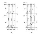
- 4A and 4B are explanatory diagrams showing the transition of the current waveform and the voltage waveform.
- FIG. 4A shows a current discontinuous mode in which the inductor current becomes discontinuous
- FIG. 4B shows the inductor current becomes continuous. Current continuous mode is shown.
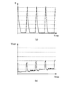
- 5A and 5B are explanatory diagrams showing experimental results using the inrush current suppression circuit.
- FIG. 5A is an explanatory diagram showing a transition of the inductor current IL
- FIG. 5B is a voltage across the input capacitor 10. It is explanatory drawing which shows transition with
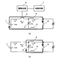
- FIG. 1 is a circuit diagram showing a configuration of an inrush current suppressing circuit according to the present embodiment.
- the inrush current suppression circuit according to the present embodiment outputs power to a load with the DC power supply 1 as an input, and suppresses an inrush current flowing from the DC power supply 1 (for example, a battery) to the load.
- the inrush current suppression circuit is mainly composed of an FET 5, first and second inductors 8, and a free wheel diode 9.
- the load includes an input capacitor 10 and a pair of output terminals 3 and 4, for example, an inverter.
- the input capacitor 10 is connected to the DC power source 1 through an inrush current suppression circuit, and is positioned on the input side of the pair of output terminals 3 and 4.
- the pair of output terminals 3 and 4 are connected in parallel to the input capacitor 10 and output an input current from the DC power supply 1.
- a load element (not shown) is connected between these output terminals 3 and 4.
- One output terminal 3 corresponds to the positive side of the DC power supply 1
- the other output terminal 4 corresponds to the ground side of the DC power supply 1.
- FET 5 is a switching element that is connected to the DC power source 1 and controlled to be turned on / off. Specifically, the drain of the FET 5 is connected to the positive electrode side of the DC power supply 1, and the source of the FET 5 is connected to one output terminal 3 via the first inductor 8. The gate of the FET 5 is connected to the drive circuit 6. The FET 5 is turned on (conductive) when an on-control signal is input to the gate of the FET 5, and is turned off (non-conductive) when an off-control signal is input to the gate of the FET 5. It is also possible to use switching elements other than FETs (field effect transistors).
- the drive circuit 6 outputs an on / off control signal based on a high-frequency pulse signal from an oscillation circuit 7 described later, and applies a predetermined control voltage to the gate of the FET 5.
- the oscillation circuit 7 controls the output of the drive circuit 6 and outputs a high frequency pulse signal to the drive circuit 6. Through the drive circuit 6 and the oscillation circuit 7, the switching frequency and duty of the FET 5 can be set.
- the first inductor 8 is provided on the positive electrode side of the DC power supply 1. Specifically, the first inductor 8 covers at least a part of the power source and the electric wire connected between the connection point between one output terminal 3 and one electrode of the input capacitor 10 and the source of the FET 5. It is comprised with the magnetic body.
- the second inductor 8 is provided on the ground side of the DC power source 1 and is connected between the connection point between the other electrode of the input capacitor 10 and the other output terminal 4 and the anode of the free-wheeling diode 9. And a magnetic body that covers at least a part of the electric wire.
- the inductance values of the first and second inductors 8 are set to be the same.
- the free-wheeling diode 9 has a cathode connected to a connection point between the FET 5 and the first inductor 8.
- the anode of the free-wheeling diode 9 is connected to the side opposite to the connection point between the other electrode of the input capacitor 10 and the other output terminal 4 when viewed from the second inductor 8.
- FIG. 2 is an explanatory diagram schematically showing the configuration of the first and second inductors 8.
- the first and second inductors 8 (hereinafter collectively referred to as “inductor 8”) are composed of a magnetic body 20.
- the magnetic body 20 is an annular member having a certain length in the axial direction, and is a magnetic body molded from a magnetic material.
- the radial length of the annular portion that is, the length from the inner diameter portion to the outer diameter portion where the electric wire L is inscribed is “a”, and the axial length is “h”.
- the magnetic body 20 is configured so that an electric wire L as a current path is inserted through an inner diameter portion thereof and covers the periphery of the electric wire L.
- the selection of the magnetic material used as the magnetic body 20 depends on the energization current in the electric wire L. For example, when a large current of up to about 300 A is supplied, it is preferable to select one having a large saturation magnetic flux density such as permendur or electromagnetic soft iron.
- FIG. 3A and 3B are explanatory views schematically showing the operating principle of the inrush current suppression circuit according to the present embodiment.
- FIG. 3A shows the state in which the FET 5 is on
- FIG. 3B shows the state in which the FET 5 is off. Indicates the state.
- FIG. 4 is an explanatory diagram showing the transition of the current waveform and voltage waveform of each part.
- FIG. 4 (a) shows a current discontinuous mode in which the inductor current is discontinuous
- FIG. 4 (b) shows a continuous inductor current. The current continuous mode is shown.
- the input capacitor 10 Since the input capacitor 10 is charged when the FET 5 is turned on, a large current tends to flow through the drain current Id. However, due to the back electromotive voltage of the inductor 8, the increase in the drain current Id increases with a certain slope as shown in FIGS. This inclination depends on the inductance value of the inductor 8. Further, the peak value of the current can be controlled by the on time and the inductance value. When the FET 5 is turned off, the drain current Id does not flow.
- the operation mode can be switched to the current continuous mode (FIG. 4A) or the current discontinuous mode (FIG. 4B).
- the drain current Id flows as the inductor current IL.
- the diode current Idio flows as the inductor current IL.
- the peak value tends to gradually decrease as the input capacitor 10 is charged.
- the peak value increases until a certain time as the input capacitor 10 is charged, but then decreases, and when the input capacitor 10 is fully charged, the peak value becomes a constant value. The tendency to take. Note that the state shown in FIG. 4 represents an initial state corresponding to the inrush current, and does not represent all of the above-described trends.
- each of the above parameters can be determined by conditions such as operating frequency, duty ratio, inductance value, switching element (maximum rating), diode (maximum rating), precharge time, and the like.
- FIG. 5 is an explanatory diagram showing an experimental result using an inrush current suppression circuit in which predetermined parameters are set.
- FIG. 5A is an explanatory diagram showing the transition of the inductor current IL
- FIG. 5B is an explanatory diagram showing the transition of the voltage Vcon across the input capacitor 10.
- FIG. 5 shows a state where the inrush current (inductor current IL) is suppressed in the current discontinuous mode. Note that the voltage of about 12 to 15 V applied across the input capacitor 10 when the FET 5 is on is due to the equivalent series resistance of the capacitor.
- the inrush current suppression circuit suppresses inrush current flowing through the load.
- This load is connected in parallel to the input capacitor 10 connected to the power source 1 and the input capacitor 10 to supply power. 1 is provided with a pair of output terminals 3 and 4 for outputting an input current from 1.
- the inrush current suppression circuit is connected between the FET 5 connected to the DC power source 1 and controlled to be turned on / off, and the connection point (the connection point between one output terminal 3 and one electrode of the input capacitor 10) and the FET 5.
- the 1st and 2nd inductor 8 is comprised from the magnetic body 20 which covers the circumference
- the inrush current suppression circuit has no inductor 8 and that the FET 5 is turned on from off.
- the input capacitor 10 is charged, so that a large current flows in a short time. Due to this current (rush current), the FET 5 is destroyed, and the interruption operation cannot be performed.
- the provision of the inductor 8 can suppress the flow of a large current. As a result, it is possible to solve the problem that the FET 5 is destroyed and the blocking operation cannot be performed.
- the magnetic body 20 as the inductor 8
- work which winds an electric wire can be abbreviate
- the inductor 8 having the same inductance value on both the positive side and the ground side, it is possible to prevent the common mode noise from changing to the normal mode noise by reducing the bias of the circuit. The adverse effects of can be reduced.
- the magnetic body 20 When the magnetic body 20 is used as the inductor 8, there are many elements that must be taken into consideration, such as the BH curve, frequency characteristics, dimensions (a, h) of the magnetic body, the value of the current flowing through the wire, and the operating frequency. In addition, it is difficult to uniformly determine the magnetic field in the magnetic material at the time of design because the current value is not constant and the magnetic material has a width. Therefore, it is preferable that the magnetic body 20 is divided into a ring shape along the axial direction, and the axial length h is made variable by selecting the number of the divided annular elements. Thereby, since the axial length h can be easily changed at the time of manufacture, an error in designing can be absorbed.
- the inrush current suppression circuit has been described above, but the present invention is not limited to this embodiment, and various modifications can be made within the scope of the present invention.
- the “power source” is not limited to a direct current output as is the case with a primary battery or a secondary battery, but may be a type that outputs a direct current by rectifying the output of the alternating current power supply with a rectifier.
- the AC power supply itself may be used.
- the inductance values of the first and second inductors are set to be the same, but it is not necessary that they are strictly matched. There may be.
- Inrush current flowing in a load including an input capacitor (10) connected to a power source (1) and a pair of output terminals (3, 4) connected in parallel to the input capacitor and outputting an input current from the power source Inrush current suppression circuit that suppresses A switching element (FET5) connected to the power source and controlled to be turned on / off; A first inductor (8) connected between a connection point between one output terminal and one electrode of the input capacitor and the switching element; A diode (9) for connecting a cathode to a connection point between the switching element and the first inductor; A second inductor (8) connected between a connection point between the other electrode of the input capacitor and the other output terminal, and an anode of the diode; The first inductor and the second inductor are an inrush current suppression circuit configured by a magnetic body that covers a wire that is a current path.
- the magnetic body includes a plurality of annular elements divided along the axial direction, and the length in the axial direction can be changed by selecting the number of
- the inductor is made of a magnetic material, it is possible to suppress the enlargement of the circuit and simplify the manufacturing work.
- the present invention that exhibits this effect is useful for an inrush current suppression circuit.
Landscapes
- Engineering & Computer Science (AREA)
- Power Engineering (AREA)
- Emergency Protection Circuit Devices (AREA)
- Direct Current Feeding And Distribution (AREA)
- Dc-Dc Converters (AREA)
Priority Applications (2)
| Application Number | Priority Date | Filing Date | Title |
|---|---|---|---|
| CN201580004825.3A CN105917540A (zh) | 2014-02-18 | 2015-02-17 | 浪涌电流抑制电路 |
| US15/208,817 US20160336739A1 (en) | 2014-02-18 | 2016-07-13 | Inrush current suppression circuit |
Applications Claiming Priority (2)
| Application Number | Priority Date | Filing Date | Title |
|---|---|---|---|
| JP2014028150A JP2015154656A (ja) | 2014-02-18 | 2014-02-18 | 突入電流抑制回路 |
| JP2014-028150 | 2014-02-18 |
Related Child Applications (1)
| Application Number | Title | Priority Date | Filing Date |
|---|---|---|---|
| US15/208,817 Continuation US20160336739A1 (en) | 2014-02-18 | 2016-07-13 | Inrush current suppression circuit |
Publications (1)
| Publication Number | Publication Date |
|---|---|
| WO2015125793A1 true WO2015125793A1 (ja) | 2015-08-27 |
Family
ID=53878294
Family Applications (1)
| Application Number | Title | Priority Date | Filing Date |
|---|---|---|---|
| PCT/JP2015/054346 Ceased WO2015125793A1 (ja) | 2014-02-18 | 2015-02-17 | 突入電流抑制回路 |
Country Status (4)
| Country | Link |
|---|---|
| US (1) | US20160336739A1 (enExample) |
| JP (1) | JP2015154656A (enExample) |
| CN (1) | CN105917540A (enExample) |
| WO (1) | WO2015125793A1 (enExample) |
Cited By (1)
| Publication number | Priority date | Publication date | Assignee | Title |
|---|---|---|---|---|
| JP2016144351A (ja) * | 2015-02-04 | 2016-08-08 | 矢崎総業株式会社 | 突入電流抑制回路 |
Families Citing this family (3)
| Publication number | Priority date | Publication date | Assignee | Title |
|---|---|---|---|---|
| CN107069688A (zh) * | 2017-05-05 | 2017-08-18 | 西安太世德航空电器有限公司 | 一种浪涌抑制电路和浪涌抑制方法 |
| CN113541457B (zh) * | 2020-04-21 | 2023-04-25 | 株洲中车时代电气股份有限公司 | 一种变流器的预充电电路及预充电方法 |
| CN119362376B (zh) * | 2024-12-23 | 2025-05-02 | 浙江宇视科技有限公司 | 浪涌电流抑制电路及方法 |
Citations (4)
| Publication number | Priority date | Publication date | Assignee | Title |
|---|---|---|---|---|
| JPH05260736A (ja) * | 1992-03-13 | 1993-10-08 | Ricoh Co Ltd | スイッチングレギュレータ |
| JPH06327239A (ja) * | 1993-04-01 | 1994-11-25 | Siemens Ag | スイッチングレギュレータ |
| JPH08275383A (ja) * | 1995-03-28 | 1996-10-18 | Fukushima Nippon Denki Kk | 突入電流防止回路 |
| JP2002095158A (ja) * | 2000-09-08 | 2002-03-29 | Tokin Corp | 雷サージサプレッサ |
Family Cites Families (9)
| Publication number | Priority date | Publication date | Assignee | Title |
|---|---|---|---|---|
| JP2902653B2 (ja) * | 1988-10-20 | 1999-06-07 | 沖電気工業株式会社 | 直流電源装置 |
| JP4143154B2 (ja) * | 1997-12-16 | 2008-09-03 | キヤノン株式会社 | 電源装置、及び電子機器 |
| JP3816449B2 (ja) * | 2003-02-05 | 2006-08-30 | 本田技研工業株式会社 | モータ駆動装置 |
| JP2005073335A (ja) * | 2003-08-21 | 2005-03-17 | Sony Corp | スイッチング電源回路 |
| JP2005094980A (ja) * | 2003-09-19 | 2005-04-07 | Sony Corp | スイッチング電源回路 |
| JP4825837B2 (ja) * | 2008-03-31 | 2011-11-30 | 本田技研工業株式会社 | Dc/dcコンバータ及び燃料電池車両 |
| JP5644353B2 (ja) * | 2010-10-15 | 2014-12-24 | 株式会社デンソー | 負荷駆動制御装置の保護装置 |
| US8717001B2 (en) * | 2012-07-03 | 2014-05-06 | Infineon Technologies Austria Ag | Inrush current limiting circuit |
| CN203251084U (zh) * | 2013-05-28 | 2013-10-23 | 北京联动天翼科技有限公司 | 基于双向buck变换器的双向限流器 |
-
2014
- 2014-02-18 JP JP2014028150A patent/JP2015154656A/ja not_active Abandoned
-
2015
- 2015-02-17 WO PCT/JP2015/054346 patent/WO2015125793A1/ja not_active Ceased
- 2015-02-17 CN CN201580004825.3A patent/CN105917540A/zh active Pending
-
2016
- 2016-07-13 US US15/208,817 patent/US20160336739A1/en not_active Abandoned
Patent Citations (4)
| Publication number | Priority date | Publication date | Assignee | Title |
|---|---|---|---|---|
| JPH05260736A (ja) * | 1992-03-13 | 1993-10-08 | Ricoh Co Ltd | スイッチングレギュレータ |
| JPH06327239A (ja) * | 1993-04-01 | 1994-11-25 | Siemens Ag | スイッチングレギュレータ |
| JPH08275383A (ja) * | 1995-03-28 | 1996-10-18 | Fukushima Nippon Denki Kk | 突入電流防止回路 |
| JP2002095158A (ja) * | 2000-09-08 | 2002-03-29 | Tokin Corp | 雷サージサプレッサ |
Cited By (1)
| Publication number | Priority date | Publication date | Assignee | Title |
|---|---|---|---|---|
| JP2016144351A (ja) * | 2015-02-04 | 2016-08-08 | 矢崎総業株式会社 | 突入電流抑制回路 |
Also Published As
| Publication number | Publication date |
|---|---|
| CN105917540A (zh) | 2016-08-31 |
| US20160336739A1 (en) | 2016-11-17 |
| JP2015154656A (ja) | 2015-08-24 |
Similar Documents
| Publication | Publication Date | Title |
|---|---|---|
| JP6291432B2 (ja) | 突入電流抑制回路 | |
| US11018592B2 (en) | Flyback converter controller, flyback converter and methods of operation | |
| US9391532B2 (en) | System and method for a switched-mode power converter | |
| US20170155325A1 (en) | Resonant power supply device | |
| JP6350753B2 (ja) | 電源回路 | |
| JP5830915B2 (ja) | 電力変換回路 | |
| CN103403819B (zh) | 动态偏置电感器 | |
| JP6099581B2 (ja) | スイッチング電源装置 | |
| WO2015125793A1 (ja) | 突入電流抑制回路 | |
| KR20190016479A (ko) | Dc/dc 컨버터 | |
| JP4434011B2 (ja) | 直流変換装置 | |
| JP2019041531A (ja) | Llc共振コンバータ | |
| JP4434010B2 (ja) | 直流変換装置 | |
| WO2019202354A1 (ja) | 共振型電力変換装置の制御方法および共振型電力変換装置 | |
| JP6091324B2 (ja) | 直流電源装置 | |
| JP6129687B2 (ja) | スイッチング電源装置 | |
| JP5959459B2 (ja) | Dc−dcコンバータ | |
| JP5318966B2 (ja) | Dc/dcコンバータ | |
| JP5954256B2 (ja) | 制御方法 | |
| JP5597276B1 (ja) | 電源装置 | |
| US20250111980A1 (en) | Saturable-core inductor | |
| JP6711150B2 (ja) | 昇圧回路 | |
| JP2012178952A (ja) | スイッチング電源回路 | |
| JP7347010B2 (ja) | 昇降圧チョッパ回路及び直流電源装置 | |
| JP2009207272A (ja) | 直流昇圧回路 |
Legal Events
| Date | Code | Title | Description |
|---|---|---|---|
| 121 | Ep: the epo has been informed by wipo that ep was designated in this application |
Ref document number: 15752004 Country of ref document: EP Kind code of ref document: A1 |
|
| NENP | Non-entry into the national phase |
Ref country code: DE |
|
| 122 | Ep: pct application non-entry in european phase |
Ref document number: 15752004 Country of ref document: EP Kind code of ref document: A1 |