WO2015104928A1 - 発光装置用基板、発光装置および発光装置用基板の製造方法 - Google Patents
発光装置用基板、発光装置および発光装置用基板の製造方法 Download PDFInfo
- Publication number
- WO2015104928A1 WO2015104928A1 PCT/JP2014/082158 JP2014082158W WO2015104928A1 WO 2015104928 A1 WO2015104928 A1 WO 2015104928A1 JP 2014082158 W JP2014082158 W JP 2014082158W WO 2015104928 A1 WO2015104928 A1 WO 2015104928A1
- Authority
- WO
- WIPO (PCT)
- Prior art keywords
- substrate
- layer
- light emitting
- insulating layer
- emitting device
- Prior art date
- Legal status (The legal status is an assumption and is not a legal conclusion. Google has not performed a legal analysis and makes no representation as to the accuracy of the status listed.)
- Ceased
Links
Images








Classifications
-
- H—ELECTRICITY
- H10—SEMICONDUCTOR DEVICES; ELECTRIC SOLID-STATE DEVICES NOT OTHERWISE PROVIDED FOR
- H10H—INORGANIC LIGHT-EMITTING SEMICONDUCTOR DEVICES HAVING POTENTIAL BARRIERS
- H10H20/00—Individual inorganic light-emitting semiconductor devices having potential barriers, e.g. light-emitting diodes [LED]
- H10H20/80—Constructional details
- H10H20/85—Packages
- H10H20/857—Interconnections, e.g. lead-frames, bond wires or solder balls
-
- H—ELECTRICITY
- H05—ELECTRIC TECHNIQUES NOT OTHERWISE PROVIDED FOR
- H05K—PRINTED CIRCUITS; CASINGS OR CONSTRUCTIONAL DETAILS OF ELECTRIC APPARATUS; MANUFACTURE OF ASSEMBLAGES OF ELECTRICAL COMPONENTS
- H05K1/00—Printed circuits
- H05K1/02—Details
- H05K1/0274—Optical details, e.g. printed circuits comprising integral optical means
-
- H—ELECTRICITY
- H05—ELECTRIC TECHNIQUES NOT OTHERWISE PROVIDED FOR
- H05K—PRINTED CIRCUITS; CASINGS OR CONSTRUCTIONAL DETAILS OF ELECTRIC APPARATUS; MANUFACTURE OF ASSEMBLAGES OF ELECTRICAL COMPONENTS
- H05K1/00—Printed circuits
- H05K1/02—Details
- H05K1/03—Use of materials for the substrate
- H05K1/05—Insulated conductive substrates, e.g. insulated metal substrate
- H05K1/053—Insulated conductive substrates, e.g. insulated metal substrate the metal substrate being covered by an inorganic insulating layer
-
- H—ELECTRICITY
- H10—SEMICONDUCTOR DEVICES; ELECTRIC SOLID-STATE DEVICES NOT OTHERWISE PROVIDED FOR
- H10H—INORGANIC LIGHT-EMITTING SEMICONDUCTOR DEVICES HAVING POTENTIAL BARRIERS
- H10H20/00—Individual inorganic light-emitting semiconductor devices having potential barriers, e.g. light-emitting diodes [LED]
- H10H20/80—Constructional details
- H10H20/85—Packages
- H10H20/852—Encapsulations
- H10H20/853—Encapsulations characterised by their shape
-
- H—ELECTRICITY
- H10—SEMICONDUCTOR DEVICES; ELECTRIC SOLID-STATE DEVICES NOT OTHERWISE PROVIDED FOR
- H10H—INORGANIC LIGHT-EMITTING SEMICONDUCTOR DEVICES HAVING POTENTIAL BARRIERS
- H10H20/00—Individual inorganic light-emitting semiconductor devices having potential barriers, e.g. light-emitting diodes [LED]
- H10H20/80—Constructional details
- H10H20/85—Packages
- H10H20/855—Optical field-shaping means, e.g. lenses
- H10H20/856—Reflecting means
-
- H—ELECTRICITY
- H10—SEMICONDUCTOR DEVICES; ELECTRIC SOLID-STATE DEVICES NOT OTHERWISE PROVIDED FOR
- H10H—INORGANIC LIGHT-EMITTING SEMICONDUCTOR DEVICES HAVING POTENTIAL BARRIERS
- H10H20/00—Individual inorganic light-emitting semiconductor devices having potential barriers, e.g. light-emitting diodes [LED]
- H10H20/80—Constructional details
- H10H20/85—Packages
- H10H20/858—Means for heat extraction or cooling
- H10H20/8581—Means for heat extraction or cooling characterised by their material
-
- H—ELECTRICITY
- H10—SEMICONDUCTOR DEVICES; ELECTRIC SOLID-STATE DEVICES NOT OTHERWISE PROVIDED FOR
- H10W—GENERIC PACKAGES, INTERCONNECTIONS, CONNECTORS OR OTHER CONSTRUCTIONAL DETAILS OF DEVICES COVERED BY CLASS H10
- H10W70/00—Package substrates; Interposers; Redistribution layers [RDL]
- H10W70/01—Manufacture or treatment
- H10W70/05—Manufacture or treatment of insulating or insulated package substrates, or of interposers, or of redistribution layers
-
- H—ELECTRICITY
- H05—ELECTRIC TECHNIQUES NOT OTHERWISE PROVIDED FOR
- H05K—PRINTED CIRCUITS; CASINGS OR CONSTRUCTIONAL DETAILS OF ELECTRIC APPARATUS; MANUFACTURE OF ASSEMBLAGES OF ELECTRICAL COMPONENTS
- H05K2201/00—Indexing scheme relating to printed circuits covered by H05K1/00
- H05K2201/10—Details of components or other objects attached to or integrated in a printed circuit board
- H05K2201/10007—Types of components
- H05K2201/10106—Light emitting diode [LED]
-
- H—ELECTRICITY
- H05—ELECTRIC TECHNIQUES NOT OTHERWISE PROVIDED FOR
- H05K—PRINTED CIRCUITS; CASINGS OR CONSTRUCTIONAL DETAILS OF ELECTRIC APPARATUS; MANUFACTURE OF ASSEMBLAGES OF ELECTRICAL COMPONENTS
- H05K2201/00—Indexing scheme relating to printed circuits covered by H05K1/00
- H05K2201/20—Details of printed circuits not provided for in H05K2201/01 - H05K2201/10
- H05K2201/2054—Light-reflecting surface, e.g. conductors, substrates, coatings, dielectrics
-
- H—ELECTRICITY
- H05—ELECTRIC TECHNIQUES NOT OTHERWISE PROVIDED FOR
- H05K—PRINTED CIRCUITS; CASINGS OR CONSTRUCTIONAL DETAILS OF ELECTRIC APPARATUS; MANUFACTURE OF ASSEMBLAGES OF ELECTRICAL COMPONENTS
- H05K3/00—Apparatus or processes for manufacturing printed circuits
- H05K3/22—Secondary treatment of printed circuits
- H05K3/28—Applying non-metallic protective coatings
- H05K3/285—Permanent coating compositions
-
- H—ELECTRICITY
- H10—SEMICONDUCTOR DEVICES; ELECTRIC SOLID-STATE DEVICES NOT OTHERWISE PROVIDED FOR
- H10W—GENERIC PACKAGES, INTERCONNECTIONS, CONNECTORS OR OTHER CONSTRUCTIONAL DETAILS OF DEVICES COVERED BY CLASS H10
- H10W90/00—Package configurations
-
- H—ELECTRICITY
- H10—SEMICONDUCTOR DEVICES; ELECTRIC SOLID-STATE DEVICES NOT OTHERWISE PROVIDED FOR
- H10W—GENERIC PACKAGES, INTERCONNECTIONS, CONNECTORS OR OTHER CONSTRUCTIONAL DETAILS OF DEVICES COVERED BY CLASS H10
- H10W90/00—Package configurations
- H10W90/701—Package configurations characterised by the relative positions of pads or connectors relative to package parts
- H10W90/721—Package configurations characterised by the relative positions of pads or connectors relative to package parts of bump connectors
- H10W90/724—Package configurations characterised by the relative positions of pads or connectors relative to package parts of bump connectors between a chip and a stacked insulating package substrate, interposer or RDL
Definitions
- the present invention relates to a light-emitting device substrate, a light-emitting device using the light-emitting device substrate, and a manufacturing method for manufacturing the light-emitting device substrate.
- the present invention relates to a light emitting device substrate having both high withstand voltage and heat dissipation.
- the performance that is basically required as a substrate for a light emitting device includes high reflectivity, high heat dissipation, dielectric strength, and long-term reliability.
- a substrate for a light-emitting device used for high-intensity illumination is required to have a high withstand voltage.
- a substrate for a light emitting device a light emitting device including a ceramic substrate or a substrate in which an organic resist layer is provided as an insulating layer on a metal substrate is known.
- the respective problems of the ceramic substrate and the substrate using the metal substrate will be mainly described.
- the ceramic substrate is manufactured by forming an electrode pattern on a plate-shaped ceramic substrate.
- it has been sought to improve the brightness by arranging a large number of light emitting elements, and as a result, ceramic substrates have been getting larger year by year.
- a general LED light-emitting device used at an input power of 30 W is, for example, a face-up type (active layer is located far from the mounting surface) blue LED element having a dimension of about 650 ⁇ m ⁇ 650 ⁇ m or around that When it is arranged on a single substrate classified as a medium size, about 100 LED elements are required.
- a ceramic substrate on which this number of LED elements are arranged for example, there is a substrate using a plane size of 20 mm ⁇ 20 mm or more and a thickness of about 1 mm.
- ceramic materials are basically ceramics, there is a problem in substrate strength when the size is increased. If the substrate is thickened to overcome this problem, a new problem arises in that the thermal resistance increases (heat dissipation becomes worse) and the material cost of the substrate also increases. In addition, when the ceramic substrate is enlarged, not only the outer dimensions of the substrate but also the dimensions of the electrode pattern formed on the substrate are likely to be distorted, resulting in a decrease in manufacturing yield and an increase in manufacturing cost of the substrate. There's a problem.
- the problem associated with such an increase in the size of the substrate, and at the same time, an increase in the number of mounted light emitting elements is also a problem.
- the number of light-emitting elements mounted on one substrate is as large as 400 or more, which contributes to a decrease in manufacturing yield.
- the active layer is located farther from the light emitting element mounting surface of the light emitting device substrate, the thermal resistance to the active layer is high and the active layer temperature is likely to rise.
- the base substrate temperature is also high, and the active layer temperature of the light-emitting elements is further increased in addition to this, and the lifetime of the light-emitting elements is significantly reduced.
- a metal substrate having high thermal conductivity may be used as a substrate for a high-power light-emitting device.
- an insulating layer must be provided on the metal substrate in order to form an electrode pattern.
- an organic resist is conventionally used as an insulating layer.
- the insulating layer needs to have high light reflectivity.
- a light-emitting device substrate having a good reflectivity, heat resistance, and light resistance can be realized with such a light-emitting device substrate in which a light-reflecting layer / insulator layer is formed on a surface of a metal substrate using a ceramic paint.
- Patent Document 5 discloses a technique for manufacturing a light source substrate by forming an insulating layer made of ceramics such as alumina on a base metal base by plasma spraying without using a paint. Yes.
- the light source substrate on which the alumina insulating layer is formed by plasma spraying can realize a good light source substrate excellent in electrical withstand voltage.
- the dielectric strength is low although the reflectance and heat dissipation are excellent.
- the high insulation pressure performance required for the light-emitting device substrate for high-intensity illumination applications is ensured. Can not.
- the insulating layer is thick, and the dielectric breakdown voltage corresponding to this is easily obtained.
- a substrate for a light emitting device in which a light reflecting layer / insulator layer is formed using a ceramic-based paint on the surface of a metal substrate, it is difficult to form the insulating layer, and the insulating property can be reproduced stably. Is difficult. Therefore, if the thickness of the light reflection layer / insulation withstand voltage layer is increased to stably secure the required high withstand voltage performance, the problem arises that this time the thermal resistance becomes higher and the heat dissipation is reduced. End up.
- the light source substrate on which an alumina insulating layer is formed by plasma spraying disclosed in Patent Document 5 is a light source substrate having excellent electrical withstand voltage and good heat dissipation, but by plasma spraying. Even if the best alumina film is obtained, the reflectance is at most about 82% to 85%, and it is difficult to realize a highly reflective substrate. Therefore, the light source substrate manufactured by the method disclosed in Patent Document 5 is suitable as a substrate for a light-emitting device used in the field of high-luminance illumination, in which a reflectance of 90% or more, further 95% or more is natural. is not.
- the surface of the alumina insulating layer formed by plasma spraying is an uneven surface, when a face-up type light emitting device is mounted on the alumina insulating layer formed by plasma spraying, the heat generated between the light emitting device and the alumina layer is reduced.
- the direct contact is limited to point contact between the lower surface of the light emitting element and the alumina layer convex portion, and the thermal resistance becomes very high.
- the active layer is easily raised because the active layer is located on the far side from the light emitting element mounting surface of the light emitting device substrate.
- the surface of the alumina insulating layer formed by plasma spraying is uneven, it is difficult to form a metal electrode.
- a base circuit pattern is formed by printing a metal paste and coated with plating so as to form an electrode on a ceramic flat plate, there is a problem in printing the paste on the uneven surface.
- the paste printing tends to cause wrinkles, which causes poor formation of plating. Further, the printing boundary becomes unclear due to the influence of the uneven surface, so that the finish of the plating becomes uneven.
- a substrate for a light emitting device using a conventional metal as a base a substrate having low thermal resistance, excellent heat dissipation, and excellent reflectivity and dielectric strength is at least suitable for mass production. Then it does not exist.
- the present invention has been made in view of the above-described conventional problems, and has the object of combining long-term reliability including high reflectivity, high heat dissipation, insulation withstand voltage, heat resistance and light resistance,
- An object of the present invention is to provide a light emitting device substrate having excellent mass productivity, a light emitting device using the light emitting device substrate, and a manufacturing method for manufacturing the light emitting device substrate.
- a light-emitting device substrate is a light-emitting device substrate including a base made of a metal material, and has a thermal conductivity formed on one surface of the base. 1 insulating layer, a wiring pattern formed on the first insulating layer, and a part of the wiring pattern so that a part of the wiring pattern is exposed. And a second insulating layer having light reflectivity formed thereon, wherein the first insulating layer is a layer made of ceramics formed by thermal spraying.
- a method for manufacturing a substrate for a light-emitting device is a method for manufacturing a substrate for a light-emitting device provided with a base made of a metal material, wherein the surface of one side of the base is thermally conductive. And a first step of forming a conductive layer on the first insulating layer, the first insulating layer and the first insulating layer so that a part of the conductive layer is exposed. Forming a second insulating layer having light reflectivity on a part of the conductive layer, and in the first step, the first insulating layer made of ceramics is formed by thermal spraying. It is characterized by forming.
- a conventional light emitting device substrate based on a general metal substrate it is necessary to sinter at a temperature lower than the melting point of the metal substrate to form an insulator layer on the metal substrate. Therefore, except for special refractory metals such as molybdenum, tantalum, and tungsten, it is difficult to obtain a high-quality and dense insulator layer. A thick insulator layer is formed.
- the light emitting device, a relatively thick insulating layer, a metal substrate, and a heat dissipation device mounted with the light emitting device substrate are used. Since heat escapes in the order of the heat sink, there arises a problem that heat dissipation is hindered by an insulating layer having a relatively large thickness.
- the wiring pattern formed on the insulator layer is generally composed of a metal paste for the electrode base and a plating layer.
- the electrode pattern is not only a path for supplying power, but also the main heat dissipation path as described above.
- the thermal conductivity of the metal paste for the electrode base is generally low, which contributes to a high thermal resistance.
- the first insulating layer made of ceramics formed by thermal spraying is formed on one surface of the base made of a metal material.
- the first insulating layer formed by thermal spraying of ceramics has the same insulating properties and thermal conductivity as the insulating layer made of ceramics obtained by sintering. Further, since the first insulating layer formed by ceramic spraying is a high-quality and dense ceramic layer, it is possible to achieve a desired withstand voltage with a relatively thin layer thickness.
- the thermal resistance of the substrate is further lowered due to the thin thickness of the first insulating layer and the high thermal conductivity of the first insulating layer formed by thermal spraying. And good heat dissipation necessary for the substrate for a high-luminance light emitting device can be secured.
- the problem that the lifetime of the light emitting element is reduced due to the difference in linear expansion coefficient between the metal base and the light emitting element is as follows.
- a first insulating layer made of high-quality and dense ceramic formed by thermal spraying as an intermediate layer, for example, the intermediate layer having a linear expansion coefficient close to that of a light-emitting element formed of a sapphire substrate, for example
- the first insulating layer functions as a buffer layer, it is possible to suppress a reduction in the lifetime of the light emitting element due to the expansion and contraction of the metal substrate.
- the range in which the type of metal substrate can be selected widens.
- the first insulating layer is formed by thermal spraying of ceramics, a metal material having a melting point lower than the sintering temperature of ceramics is used. Even on the substrate, a high-quality and dense first insulating layer can be formed. Therefore, it is possible to realize a light emitting device substrate and a method for manufacturing a light emitting device substrate that are excellent in mass productivity.
- the light emitting device substrate and the light emitting device substrate manufacturing method according to the present invention include light formed on the first insulating layer and on a part of the wiring pattern so that a part of the wiring pattern is exposed. Since the reflective second insulating layer is formed, a light-emitting device substrate having a high reflectance and a method for manufacturing the light-emitting device substrate can be realized.
- the first insulating layer is a layer made of ceramics
- the light emitting device substrate having high long-term reliability including heat resistance and light resistance is provided. Can be realized.
- a light-emitting device having high reflectivity, high heat dissipation, long-term reliability including withstand voltage, heat resistance and light resistance, and excellent mass productivity.
- the manufacturing method of the substrate for light and the substrate for light emitting device can be realized.
- a light emitting device of the present invention includes a light emitting element that is electrically connected to a terminal portion of the wiring pattern exposed from the second insulating layer in the substrate for the light emitting device, and the wiring pattern Are connected to an external wiring or an external device, and are formed of a light-reflective resin frame portion that surrounds a region where the light emitting element is disposed on the light emitting device substrate, and the frame portion. And a sealing resin that seals a region surrounded by is formed.
- a substrate for a light emitting device that combines high reflectivity, high heat dissipation, withstand voltage, long-term reliability including heat resistance and light resistance, and excellent in mass productivity. Therefore, it is possible to realize a light emitting device that has high reflectivity, high heat dissipation, dielectric strength, long-term reliability including heat resistance and light resistance, and excellent mass productivity.
- a light emitting device substrate of the present invention, a light emitting device using the light emitting device substrate, and a manufacturing method for manufacturing the light emitting device substrate have high reflectivity, high heat dissipation, dielectric strength, and long-term reliability. It is possible to provide a substrate for a light emitting device that has both high performance and excellent mass productivity, a light emitting device using the substrate for light emitting device, and a manufacturing method for manufacturing the substrate for light emitting device.
- FIG. 1 is a plan view showing a schematic configuration of a light emitting device 1.
- FIG. It is sectional drawing which shows schematic structure of the board
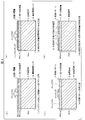
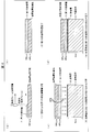
- FIG. 5 is a diagram for explaining a manufacturing process of the light emitting device substrate 20a.
- FIG. 5 is a diagram for explaining a manufacturing process of the light emitting device substrate 20a.
- 2 is a cross-sectional view showing a schematic configuration of a substrate for a light emitting device in which a first insulating layer 11 is also formed on a side surface of a metal substrate 2 as a protective film.
- substrate 2) facing the surface in which the 1st insulating layer 11 is formed is shown. It is sectional drawing. It is a figure which shows typically the cut surface of the light-emitting device provided with board
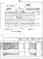
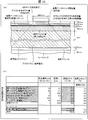
- (A) is a figure which shows typically the cut surface of the light-emitting device provided with the board
- (b) is a figure which shows the trial calculation result of the thermal resistance in this light-emitting device.
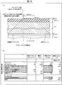
- (A) is a figure which shows typically the cut surface of the light-emitting device of the comparative example 1
- (b) is a figure which shows the trial calculation result of the thermal resistance in this light-emitting device.
- (A) is a figure which shows typically the cut surface of the light-emitting device provided with the board
- (b) is a figure which shows the trial calculation result of the thermal resistance in this light-emitting device. .
- (A) is a figure which shows typically the cut surface of the light-emitting device of the comparative example 2
- (b) is a figure which shows the trial calculation result of the thermal resistance in this light-emitting device.
- (A) is a figure which shows typically the cut surface of the light-emitting device of the comparative example 3
- (b) is a figure which shows the trial calculation result of the thermal resistance in this light-emitting device.
- FIGS. 1 to 9 Embodiments of the present invention will be described with reference to FIGS. 1 to 9 as follows.
- FIG. 1 is a plan view showing a schematic configuration of a light emitting device 1 according to the present embodiment.
- FIG. 2 is a cross-sectional view showing a schematic configuration of the light emitting device substrate 20 provided in the light emitting device 1 shown in FIG.
- the light-emitting device 1 includes a metal substrate 2, a first insulating layer 11 (shown in FIG. 2), a wiring pattern 3, and a second insulating layer 12 (see FIG. 2) and an LED chip 4.
- FIG. 1 shows nine LED chips 4 arranged in three rows and three columns.
- the nine LED chips 4 are connected in parallel in three rows by the wiring pattern 3, and each of the three rows has a connection configuration having a series circuit of three LED chips 4 (that is, 3 series / 3 parallel) It has become.
- the number of LED chips 4 is not limited to nine, and it is not necessary to have a 3 series / 3 parallel connection configuration.
- the light emitting device 1 includes a light reflecting resin frame 5, a phosphor-containing sealing resin 6, an anode electrode (anode land) 7, a cathode electrode (cathode land) 8, an anode mark 9, and a cathode mark 10. It is equipped with.
- the light reflecting resin frame 5 is an annular (arc-shaped) frame made of an alumina filler-containing silicone resin provided on the wiring pattern 3 and the second insulating layer 12.
- the material of the light reflecting resin frame 5 is not limited to this, and may be any insulating resin having light reflectivity, and the shape thereof is not limited to an annular shape (arc shape), but may be an arbitrary shape. be able to.
- the phosphor-containing sealing resin 6 is a sealing resin layer made of a translucent resin.
- the phosphor-containing sealing resin 6 is filled in a region surrounded by the light reflecting resin frame 5 and seals the wiring pattern 3, the LED chip 4, and the second insulating layer 12.
- the phosphor-containing sealing resin 6 contains a phosphor.
- As the phosphor a phosphor that is excited by the primary light emitted from the LED chip 4 and emits light having a longer wavelength than the primary light is used.
- the configuration of the phosphor is not particularly limited, and can be appropriately selected according to desired white chromaticity and the like.
- a combination of YAG yellow phosphor and (Sr, Ca) AlSiN 3 : Eu red phosphor, a combination of YAG yellow phosphor and CaAlSiN 3 : Eu red phosphor, etc. as a combination of daylight white color and light bulb color Can be used.
- As a combination of high color rendering (Sr, Ca) AlSiN 3 : Eu red phosphor and Ca 3 (Sc, Mg) 2 Si 3 O 12 : Ce green phosphor or Lu 3 Al 5 O 12 : Ce green phosphor
- the combination of another fluorescent substance may be used and the structure containing only a YAG yellow fluorescent substance as pseudo white may be used.
- the anode electrode (anode land) 7 and the cathode electrode (cathode land) 8 are electrodes for supplying a current for driving the LED chip 4 to the LED chip 4 and are provided in the form of lands.
- the anode electrode (anode land) 7 and the cathode electrode (cathode land) 8 are electrodes that can be connected to an external power source (not shown) in the light emitting device 1.
- the anode electrode (anode land) 7 and the cathode electrode (cathode land) 8 are connected to the LED chip 4 via the wiring pattern 3.
- the anode mark 9 and the cathode mark 10 are alignment marks serving as references for positioning with respect to the anode electrode (anode land) 7 and the cathode electrode (cathode land) 8, respectively.
- the anode mark 9 and the cathode mark 10 have a function of indicating the polarities of the anode electrode (anode land) 7 and the cathode electrode 8, respectively.
- the thickness of the portion of the wiring pattern 3 immediately below the anode electrode (anode land) 7 and the cathode electrode (cathode land) 8 is larger than the thickness of the portion of the wiring pattern 3 other than the portion directly below the anode electrode (anode land) 7.
- the thickness of the wiring pattern 3 is 70 ⁇ m or more and 300 ⁇ m or less immediately below the anode electrode (anode land) 7 and the cathode electrode (cathode land) 8, and is 35 ⁇ m or more and 250 ⁇ m or less in the portion other than the portion immediately below the anode pattern. Is preferred.
- the wiring pattern 3 exceeds 300 ⁇ m and the wiring pattern 3 is thicker, the LED chip 4 can be sufficiently spaced. The thermal resistance is lowered and the heat dissipation is improved.
- the thermal resistance can be lowered.
- the thickness of the wiring pattern 3 is 300 ⁇ m immediately below the anode electrode (anode land) 7 and the cathode electrode (cathode land) 8, and 250 ⁇ m or less in other portions. It is not limited to this depending on the application.
- the total sum of the bottom areas of the wiring patterns 3 is preferably at least four times the total area of the electrode terminals on which the LED chips 4 are mounted in the wiring patterns 3.
- the thermal conductivity of the first insulating layer 11 shown in FIG. 2 is lower than the thermal conductivity of the wiring pattern 3, and the wiring pattern 3 has a sufficiently large area in contact with the first insulating layer 11. The thermal resistance received by the heat passing through the first insulating layer 11 can be lowered.
- the ratio of the above areas is set to 4 times or more, but the thermal conductivity is lower than this, for example, 7.5 W / In the case of (m ⁇ ° C.), it is desirable to make it 8 times or more, and it is desirable to take the total sum of the bottom areas of the wiring patterns as much as possible as the thermal conductivity is lower.
- the light emitting device substrate 20 includes a base 2 made of a metal material, a first insulating layer 11 having thermal conductivity formed on one surface of the base 2, and The wiring pattern 3 formed on the first insulating layer 11 and the wiring pattern 3 are formed on the first insulating layer 11 and a part of the wiring pattern 3 so that a part of the wiring pattern 3 is exposed. And a second insulating layer 12 having light reflectivity.
- an aluminum substrate is used as the substrate 2 made of a metal material.
- the aluminum substrate for example, an aluminum plate having a length of 50 mm, a width of 50 mm, and a thickness of 3 mm can be used.
- Advantages of aluminum include light weight, excellent workability, and high thermal conductivity.
- the aluminum substrate may contain components other than aluminum to the extent that the anodizing treatment is not hindered.
- the first insulating layer 11, the wiring pattern 3, and the second insulating layer 12 having light reflectivity are formed on the substrate 2 at a relatively low temperature. Therefore, an aluminum substrate that is a low melting point metal having a melting point of 660 ° C. can be used as the substrate 2 made of a metal material.
- the substrate is not limited to an aluminum substrate.
- a wide range of materials can be selected as the substrate 2 made of a metal material such as a copper substrate.
- First insulating layer having thermal conductivity In the present embodiment, as shown in FIG. 2, in order to stably provide the heat-emitting device substrate 20 with high heat dissipation and high withstand voltage characteristics, a thermally conductive ceramic insulator is used. A certain first insulating layer 11 is formed between the base 2 made of a metal material and the wiring pattern 3 or the second insulating layer 12 having light reflectivity.
- the first insulating layer 11 is an insulating layer that is formed by thermal spraying on the base 2 made of a metal material and has good thermal conductivity. Since the first insulating layer 11 does not use a binder that lowers thermal conductivity like glass or resin, it does not impair the high thermal conductivity inherent in ceramics. Compared to the insulating layer formed in this way, the same withstand voltage can be realized with a low thermal resistance.
- the aluminum substrate which is a low melting metal having a melting point of 660 ° C.
- the substrate 2 made of a metal material a ceramic sintered body is placed on the aluminum substrate.
- the first insulating layer 11 cannot be formed by direct sintering, the first insulating layer 11 can be formed on the aluminum substrate by spraying.
- the first insulating layer made of only ceramics can be easily formed without using a binder made of glass or resin.
- the first insulating layer 11 having high heat dissipation and high withstand voltage characteristics can be formed on the light emitting device substrate 20, the light emitting device substrate 20 has high heat dissipation, High dielectric strength characteristics can be stably imparted.
- alumina is desirable because it has a good balance between insulation and thermal conductivity.
- alumina is used, but the present invention is not limited to this.
- aluminum nitride and silicon nitride are preferable because both thermal conductivity and withstand voltage performance are good.
- silicon carbide has high thermal conductivity, and zirconia and titanium oxide have high withstand voltage performance. Therefore, it is preferable to properly use the first insulating layer 11 according to the purpose and application.
- the ceramics referred to here are not limited to metal oxides, but include ceramics in a broad sense including aluminum nitride, silicon nitride, silicon carbide and the like, that is, inorganic solid materials in general. Of these inorganic solid materials, any material may be used as long as it is a stable material excellent in heat resistance and thermal conductivity and excellent in dielectric strength.
- the first insulating layer 11 is preferably higher than the thermal conductivity of ceramic particles that can be used for the second insulating layer 12 described later in detail.
- an insulating layer made of alumina having a higher thermal conductivity than zirconia is used as the first insulating layer 11, which is the second insulating layer 12 in the present embodiment. This is also because an insulating layer containing zirconia particles is used. Also, in order to form an electrical insulating layer by thermal spraying, it is most common to spray alumina to form an insulating layer made of alumina. Such an insulating layer made of alumina has a thermal conductivity and It is also preferable because both of the dielectric strength performance are good.
- the first insulating layer 11 and the second insulating layer 12 to be described later are both insulating layers.
- the second insulating layer 12 having light reflectivity should have a minimum thickness that can ensure a light reflecting function. Is enough.
- the second insulating layer 12 having light reflectivity generally saturates at a layer thickness of 10 ⁇ m to 100 ⁇ m, depending on the ceramic material to be mixed and its amount.
- the withstand voltage of the first insulating layer 11 depends on the formation conditions of the insulating layer, the first insulating layer 11 is preferably formed with a thickness of 50 ⁇ m to 500 ⁇ m.
- the dielectric strength performance of the first insulating layer 11 formed by thermal spraying is approximately 15 kV / mm to 30 kV / mm, for example, if the first insulating layer 11 is formed with a thickness of 100 ⁇ m, The insulation voltage resistance of 1.5 kV to 3 kV or more can be secured at least by one insulating layer 11, and if it is formed with a thickness of 500 ⁇ m, the insulation of at least 7.5 kV to 15 kV can be achieved only by the first insulating layer 11. Pressure resistance can be ensured.
- the first insulating layer 11 is formed so that the withstand voltage between the base 2 and the wiring pattern 3 is about 4 kV to 5 kV. It is required to design the layer thickness. With a thickness of at least 300 ⁇ m, a dielectric breakdown voltage of 4.5 kV can be realized.
- the thermal conductivity of the ceramic layer formed by thermal spraying is close to the thermal conductivity of the ceramic layer formed by sintering, for example, a value of 10-30 W / (m ⁇ ° C.).
- an insulating layer formed by solidifying ceramic particles using a binder made of glass or resin is usually about 1-3 W / (m ⁇ ° C.) due to the low thermal conductivity of glass or resin.
- the thermal conductivity of the ceramic layer formed by thermal spraying is one order of magnitude higher than that of an insulating layer formed by solidifying ceramic particles using a binder made of glass or resin. It can be said.
- the thermal resistance of the insulating layer made of alumina formed by thermal spraying used as the first insulating layer 11 is about the same as that of the insulating layer formed by solidifying alumina particles with a binder made of glass or resin.
- the former layer thickness of 500 ⁇ m and the latter layer thickness of 50 ⁇ m are approximately the same thermal resistance. If the withstand voltage performance per thickness is the same, even if the former secures a withstand voltage 10 times that of the latter, the heat dissipation is the same.
- the inside of the first insulating layer 11 may be further composed of a plurality of layers as appropriate.
- Thermal spraying is a method in which molten particles obtained from a thermal spray material that has been melted or heated to a state close to it are made to collide with the surface of the substrate at high speed, and the thermal spray material is sprayed in the form of powder or wire. Supplied to the device. Thermal spraying is classified into flame spraying, arc spraying, plasma spraying, high-speed flame spraying, etc., depending on the method of heating the sprayed material. A cold spray method in which a coating is formed by impinging on a base material in a solid state in supersonic flow together with an inert gas without melting the material is also classified as a kind of thermal spraying. For the purpose of forming the ceramic layer on the metal substrate, high-speed flame spraying, plasma spraying, and flame spraying are appropriate. Hereinafter, high-speed flame spraying, plasma spraying, and flame spraying will be described.
- a high adhesion force and a dense alumina layer can be formed.
- the porosity ratio of air holes in the formed film
- pressure resistance can be realized.
- the thickness of the insulating layer obtained by this method is currently limited to about 400 ⁇ m.
- plasma spraying working gas such as argon is ionized by arc discharge to generate plasma.
- This plasma is used to heat and melt a high melting point thermal spray material such as ceramics, put it on a plasma flow ejected from a nozzle, accelerate the molten particles, and collide with the substrate surface at a high speed to laminate the ceramics.
- the temperature rise of the substrate at the time of laminating the ceramic layer is about 200 ° C. at the maximum, and the porosity is about 1% -5%, which is slightly higher than high-speed flame spraying. Care must be taken not to create through holes.
- the present invention is not limited to this, and the ceramic layer may be formed by plasma spraying. Further, the thickness of the ceramic layer may be increased. Other spraying methods such as flame spraying can also be used by adjusting as appropriate.
- the wiring pattern 3 formed on the first insulating layer 11 can be formed by a conventional wiring pattern forming method.
- the wiring pattern is used for an electrode base. It is composed of a metal paste and a plating layer.
- an electrode base metal paste uses an organic substance such as a resin as a binder, which is a cause of low thermal conductivity and high thermal resistance.
- the surface of the first insulating layer 11 formed by thermal spraying is usually uneven as it is. If an attempt is made to form a base circuit pattern by printing a metal paste directly on the concave and convex surface, the base circuit pattern is affected by the concave and convex, and printing may be blurred or an unclear portion may be printed. These cause a deposition failure of the plating and, in particular, a short circuit between the electrode terminals in the light emitting element mounting portion.
- a copper conductive layer is formed on the first insulating layer 11 by high-speed flame spraying to form the wiring pattern 3.
- the copper conductive layer is formed directly on the first insulating layer 11 by high-speed flame spraying. Since the adhesiveness with the wiring pattern 3 is good and a high resistance layer with low thermal conductivity is not interposed therebetween, the light emitting device substrate 20 having good heat dissipation can be realized. In addition, since the wiring pattern 3 is finally scraped from the conductive layer by etching after the conductive layer is formed, electrode formation defects and short-circuits between the electrode terminals at the light emitting element mounting portion do not occur.
- copper is formed as the conductive layer for forming the wiring pattern 3.
- the present invention is not limited to this, and a conductive layer such as silver may be formed.
- the widely used high-speed flame spraying is used, but the present invention is not limited to this, and other spraying methods can also be used.
- plasma spraying or a cold spray method may be used.
- the cold spray method which uses an inert gas as a carrier gas and collides with a base material in the solid state in supersonic flow together with the inert gas without melting the material to form a coating, oxidizes the conductive layer.
- the cold spray method which uses an inert gas as a carrier gas and collides with a base material in the solid state in supersonic flow together with the inert gas without melting the material to form a coating, oxidizes the conductive layer.
- it is one of the effective means that can be selected.
- the exposed portion of the wiring pattern 3 includes a terminal portion electrically connected to the light emitting element, an anode electrode (anode land) 7 and a cathode electrode (cathode land) 8 connected to an external wiring or an external device, and an anode. These are the mark 9 and cathode mark 10 portions.
- the anode mark 9 and the cathode mark 10 may be formed on the second insulating film 12.
- the anode electrode (anode land) 7 and the cathode electrode (cathode land) 8 may be connected to the external wiring or the external device by soldering. Alternatively, it may be connected to an external wiring or an external device through connectors respectively connected to the anode electrode (anode land) 7 and the cathode electrode (cathode land) 8.
- the second insulating layer 12 is made of an insulating material that reflects light from the LED chip 4.
- the second insulating layer 12 is formed of an insulating layer containing ceramics, and the thickness of the second insulating layer 12 is 10 ⁇ m, for example, considering the reflectance of the light emitting device substrate 20. It can be about 500 ⁇ m. The upper limit of this thickness is limited by the thickness of the wiring pattern 3. If the copper wiring pattern 3 is exposed, it absorbs light. Therefore, the copper wiring pattern 3 needs to have a sufficient thickness to cover all of the wiring pattern 3 except for the part that needs to be exposed.
- the second insulating layer 12 should also have an optimum thickness of 300 ⁇ m or less in order to cover it.
- the optimum thickness should be 500 ⁇ m or less.
- the layer thickness of the second insulating layer 12 is the minimum thickness necessary for obtaining a desired reflectance. It is preferable to set the layer thickness to about 50 ⁇ m to 100 ⁇ m to achieve this purpose. If the maximum thickness of the wiring pattern 3 is large and cannot be sufficiently covered with this thickness, a third insulating layer may be interposed between the first insulating layer 11 and the second insulating layer 12. It is desirable that the thermal conductivity of is higher than that of the second insulating layer 12.
- the third insulating layer may be an insulating layer containing ceramic particles having good heat dissipation in a glass binder or resin binder, may be a ceramic layer formed by thermal spraying, and further the first insulating layer.
- the same alumina layer may be used.
- the light-reflective second insulating layer 12 is made of an insulating layer containing zirconia particles that are light-reflective ceramic particles, and this insulating layer is sintered by using a glass-based binder. Forming.
- an aluminum base is used as the base 2 made of a metal material, and an insulating layer made of alumina, which is a ceramic layer, is used as the first insulating layer 11. Therefore, in the formation process of the second insulating layer 12 formed in a subsequent process, it is possible to raise the firing temperature to below the melting point of the base 2 made of a metal material.
- the synthesis of vitreous by the sol-gel method is usually performed at 200 ° C. to 500 ° C., but 400 ° C. to 500 ° C. is used in order to reduce the number of holes from the porous film generated in the vitreous gel state and increase the insulation. It is preferable to perform firing.
- the sol used for the vitreous synthesis by the sol-gel method is used as a binder of zirconia particles so that a part of the wiring pattern 3 is exposed so that the first insulating layer 11 is exposed.
- a second insulating layer 12 having light reflectivity is applied on the top and a part of the wiring pattern 3 by screen printing, dried at 200 ° C. to 300 ° C., and baked to a finish at 400 ° C. to 500 ° C. Yes.
- the second insulating layer 12 having light reflectivity may be formed using spray coating.
- a part of the second insulating layer 12 can be polished to expose a part of the wiring pattern 3. .
- zirconia particles are used as the light-reflective ceramic particles.
- the present invention is not limited to this, and titanium oxide, aluminum nitride, or the like can be used in addition to zirconia.
- alumina can be used as the light-reflective ceramic particles.
- the ceramics referred to here are not limited to metal oxides, but are broadly defined ceramics including aluminum nitride, and include all inorganic solid materials. Of these inorganic solid materials, any material can be used as long as it is a stable material excellent in heat resistance and thermal conductivity and excellent in light reflection and light scattering. However, ceramic particles that cause light absorption are not suitable. Specifically, silicon nitride, silicon carbide, and the like are generally black and are not suitable as ceramic particles used for the second insulating layer 12.
- a glass-based binder is sintered using a sol-gel method with a firing temperature of 400 ° C. to 500 ° C.
- the 2nd insulating layer 12 was formed, it is not limited to this, It can also form using methods other than a sol gel method.
- a vitreous layer by remelting particles of low-melting glass with an organic binder. At least a temperature of 800 ° C. to 900 ° C. is necessary for remelting.
- a ceramic layer typified by alumina is used as the first insulating layer 11, the following is performed.
- a method of forming the second insulating layer 12 that requires such a high-temperature process can also be used.
- such a high-temperature process exceeds the melting point of the aluminum substrate of 660 ° C.
- the melting point is 1085 ° C., so it can be used as it is.
- the vitreous layer is excellent in light resistance and heat resistance, it is preferably used for forming the second insulating layer 12.
- a resin excellent in heat resistance and light resistance can also be used as an alternative to vitreous.
- the second insulating layer 12 may be formed using a silicone resin, an epoxy resin, or a fluororesin as a binder for the ceramic particles. Although it is inferior to glass in terms of heat resistance and light resistance, it has a merit that the curing temperature is lower than the glass synthesis by the sol-gel method and the forming process is easy.
- the inside of the second insulating layer 12 may be further composed of a plurality of layers as appropriate.
- a layer having high thermal conductivity can be arranged in the second insulating layer 12 close to the first insulating layer 11, and a layer having high light reflectance can be arranged in the opposite layer. Therefore, it is possible to realize a light emitting device substrate having both high reflectivity, high heat dissipation, dielectric strength, and long-term reliability including heat resistance and light resistance.
- the levels of thermal conductivity and light reflectance referred to here are relative comparisons in the second insulating layer 12.
- the LED chip 4 is mounted on the light emitting device substrate 20 and packaged.
- the LED chip 4 is electrically connected to the terminal portion of the wiring pattern 3 by flip chip bonding.
- an LED element is used as a light emitting element, but the present invention is not limited to this, and an EL element or the like can also be used.
- the light emitting element is formed of a sapphire substrate.
- the laminating step (1) of the first insulating layer 11 by thermal spraying as shown in FIG. 3 (a), one side (the first side) of a 3 mm thick aluminum substrate used as the metal substrate 2 is used.
- the first insulating layer 11 made of alumina was formed using a high-speed flame spraying apparatus after roughening the surface of the first insulating layer 11 side) by sandblasting.
- the first insulating layer 11 having a thickness of 300 ⁇ m was completed (the first insulating layer 11 was stacked (2)).
- the first insulating layer 11 may be formed using a plasma spraying apparatus instead of the high-speed flame spraying apparatus.
- the surface on one side of the aluminum substrate is roughened by sandblasting in order to improve the adhesion between the metal substrate 2 and the first insulating layer 11, but this step is necessary.
- the metal base 2 and the first insulating layer 11 may be omitted as appropriate.
- a metal conductive layer is formed on the first insulating layer 11 using a high-speed flame spraying apparatus.
- a copper conductive layer was formed to a thickness of 300 ⁇ m.
- the copper conductive layer may be formed using a plasma spraying device or the like instead of the high-speed flame spraying device.
- the cold spray method is also an effective method for reducing copper oxidation.
- the metal conductive layer is formed by thermal spraying, but the metal conductive layer may be formed by a method other than thermal spraying.
- the conductive layer may be thinly formed by thermal spraying, and then the copper conductive layer may be deposited thickly by plating.
- the electrode layer may be formed using printing of metal paste or plating as usual.
- the conductive layer formed by thermal spraying has higher adhesion and lower thermal resistance than the first insulating layer 11 formed by thermal spraying, at least a portion in contact with the first insulating layer 11 is metal conductive.
- the layer is also preferably formed by thermal spraying.
- the copper conductive layer formed to a thickness of 300 ⁇ m is polished and then dry-etched to smooth the surface. Then, a copper conductive layer having a flat surface was obtained. And the layer thickness of the copper conductive layer after this smoothing process became 200 micrometers. Note that in this embodiment, dry etching is performed after polishing as the smoothing process, but the present invention is not limited to this, and wet etching may be performed after polishing as the smoothing process.
- the metal substrate 2 faces the surface on which the first insulating layer 11 is formed.
- the back surface protection sheet 14 was formed on the surface.
- the back surface protection sheet 14 serves to prevent the metal substrate 2 from being damaged when the resist 13 is formed in a predetermined pattern.
- the back surface protection sheet 14 is provided only on the surface of the metal substrate 2 that faces the surface on which the first insulating layer 11 is formed will be described. It is preferable to provide a protective sheet. Thereafter, a resist 13 is formed on the entire surface of the copper conductive layer after the smoothing treatment, and in the copper conductive layer, a terminal portion (electrode post) for electrical connection with the light emitting element (LED chip 4), A pattern of the resist 13 was formed so that the resist 13 remained. In order to form the resist 13 in a predetermined pattern, at least coating, exposure, and development steps need to be performed. Therefore, the back surface protection sheet 14 protects the metal substrate 2 during these steps. In the present embodiment, the back surface protective sheet 14 is used.
- the present invention is not limited to this, and instead of the protective sheet, for example, an aluminum anodized film (anodized on the side surface and back surface of the aluminum substrate). Layer) may be formed. Furthermore, it is more preferable to perform a sealing process on the anodized aluminum film (alumite layer).
- the resist 13 is used as a mask to form copper as a metal conductive layer.
- the conductive layer was half-etched by dry etching to form a terminal portion (electrode post) on the copper conductive layer.
- the resist 13 is left so that the resist 13 remains in the terminal portion (electrode post) for electrical connection with the light emitting element (LED chip 4) in the copper conductive layer.
- the resist 13 is also left on the portions where the anode electrode (anode land) 7, the cathode electrode (cathode land) 8, the anode mark 9 and the cathode mark 10 are formed.
- the resist 13 shown in FIG. 4B is peeled and removed, and then, as shown in FIG. 4C, in the copper conductive layer, A resist 15 was formed so as to expose only the region between the terminal portions (electrode posts). Then, using the resist 15 as a mask, the copper conductive layer was dry-etched (or wet-etched) to electrically separate the two terminal portions (electrode posts), thereby completing the wiring pattern 3.
- the resist 15 shown in FIG. 4C is stripped and removed, and then shown in FIG. 4D.
- a glassy material containing zirconia particles is applied by screen printing so that terminal portions (electrode posts) in the copper conductive layer are exposed, dried at 200 ° C. to 300 ° C., and 400 ° C.
- the second insulating layer 12 was completed by baking at ⁇ 500 ° C. In this embodiment, since screen printing is used, a separate step of exposing the terminal portion (electrode post) is unnecessary.
- the 2nd insulating layer 12 which has light reflectivity using spray coating
- one of the 2nd insulating layers 12 is used.
- polishing a part and exposing a terminal part (electrode post) separately is needed.
- the LED chip 4 as a flip chip type light emitting element is flip-chip bonded to the terminal portion of the wiring pattern 3 on the light emitting device substrate 20 to be electrically connected, and the LED chip 4 illustrated in FIG. 2 is provided.
- the light emitting device substrate 20 was completed.
- the electrical bonding may be performed appropriately by Au bump method, soldering, or the like.
- the outer shape of the substrate 2 in the direction of the substrate surface is a hexagon, but the outer shape of the substrate 2 is not limited to this, and any closed figure shape can be adopted.
- the closed figure shape may be a closed figure shape in which the circumference of the closed figure is composed of only a straight line or only a curve, and the closed figure shape has at least one straight line portion and a circumference of the closed figure. It may be a closed figure shape including at least one curved portion. Further, the closed figure shape is not limited to the convex figure shape, and may be a concave figure shape.
- a convex polygonal shape composed only of straight lines a triangular shape, a quadrangular shape, a pentagonal shape, an octagonal shape, or the like may be used, and an arbitrary concave polygonal shape may be used.
- a closed figure shape comprised only by the curve circular shape or elliptical shape may be sufficient, and closed figure shapes, such as a convex curve shape or a concave curve shape, may be sufficient.
- a race track shape or the like may be used as an example of a closed figure shape including at least one straight line portion and at least one curved portion.
- FIG. 16 is a diagram illustrating a modification of the light emitting device substrate 20 of the first embodiment shown in FIG.
- a buffer layer 250 is formed between the metal base 2 and the first insulating layer 11 as shown in FIG. .
- the first insulating layer 11 is formed on a base made of metal such as an aluminum plate to form a light emitting device substrate, particularly when this is used as a high output light emitting device substrate.
- the base made of the metal repeatedly expands and contracts.
- the first insulating layer 11 formed on the base body is subjected to a mechanical load due to a difference in coefficient of linear expansion coefficient with the metal base body, and there is a possibility that the peeling and withstand voltage resistance may be lowered.
- a buffer layer 250 is formed between the metal base 2 and the first insulating layer 11 as shown in FIG.
- the metal substrate 2 is a substrate made of a material having high thermal conductivity.
- the material of the metal substrate 2 is not particularly limited as long as it has a high thermal conductivity.
- a substrate made of a metal containing aluminum, copper, stainless steel, or iron as a material can be used.
- the buffer layer 250 is a film formed by thermal spraying or an aerosol deposition method (AD method) on one surface (hereinafter referred to as a surface) of the metal substrate 2, and is made of a material having a smaller linear expansion coefficient than the metal substrate 2. Become. Furthermore, it is preferable that the linear expansion coefficient of the buffer layer 250 is larger than that of the first insulating layer 11.
- the thickness of the buffer layer 250 is 10 ⁇ m or more and 100 ⁇ m or less, and preferably between 20 ⁇ m and 30 ⁇ m.
- a buffer layer 250 having a linear expansion coefficient smaller than that of the metal substrate 2 and close to the first insulating layer 11 By interposing a buffer layer 250 having a linear expansion coefficient smaller than that of the metal substrate 2 and close to the first insulating layer 11, a mechanical load due to thermal expansion and contraction of the metal substrate 2 is transmitted to the light emitting element. Since it can reduce remarkably, the lifetime of LED chip 4 (light emitting element) and by extension, the light-emitting device 1 can be extended, and reliability can be improved.
- the buffer layer 250 is preferably a metal or alloy layer, and the material of the metal or alloy layer used for the buffer layer 250 is a linear expansion coefficient such as Ni, Ti, Co, Fe or Nb, Mo, Ta, W. It is a metal containing at least any one of these small metals, or an alloy.
- the buffer layer 250 includes at least one of Ni, Ti, and Co as a material, and particularly preferably, the buffer layer 250 includes Ni as a material. Is desirable.
- the buffer layer 250 is preferably an alloy of Ni (nickel) and aluminum.
- the buffer layer 250 is an alloy of Ni (nickel) and aluminum, it is desirable to increase the ratio of Ni as much as possible in order to bring the linear expansion coefficient close to an intermediate value between the metal substrate 2 and the first insulating layer 11.
- the ratio of nickel in the buffer layer 250 is desirably 90% or more by weight.
- the linear expansion coefficient of nickel is 13.4 ⁇ 10 ⁇ 6 / ° C., which is an intermediate value between the linear expansion coefficients of aluminum and alumina which is a typical ceramic material, 15 ⁇ 10 ⁇ 6 / This is due to the fact that it almost coincides with °C.
- the linear expansion coefficient of the buffer layer 250 is close to 15 ⁇ 10 ⁇ 6 / ° C., 13-16 ⁇ 10 ⁇ This is because it becomes possible to keep the temperature between 6 / ° C.
- the melting point of Ni is a low class among these metals, it is actually as high as 1455 ° C.
- the melting point can be lowered, and the temperature necessary for preparing a molten state or a semi-molten state is lowered.
- it is convenient for forming a nickel layer by thermal spraying.
- the linear expansion coefficient of Ni is approximately between aluminum and alumina, which is suitable as a buffer layer.
- the linear expansion coefficient of glass varies greatly depending on the composition, but is generally between 3-9 ⁇ 10 ⁇ 6 / ° C., which is relatively close to that of alumina.
- the buffer layer 250 is formed by thermal spraying or aerosol deposition method (AD method).
- the forming method by thermal spraying is the method as described above.
- the AD method is a technique for forming a coating film by mixing fine particles and ultrafine particle raw materials prepared in advance by other methods with a gas to form an aerosol, and spraying it onto a substrate through a nozzle.
- the surface of the substrate may be roughened by blasting or the like prior to the formation of the buffer layer 250.
- the buffer layer 250 is a metal or alloy layer, but the present invention is not limited to this, and instead the buffer layer 250 is formed using a resin processed into a sheet or a paste-like resin. Also good.
- additives may be appropriately added.
- the additive include ceramic particles, glass fibers, metal particles, and the like.
- the resin constituting the buffer layer 250 may be selected from an epoxy resin, a silicone resin, a polyimide resin, or a fluorine resin having excellent heat resistance.
- a commercially available insulating sheet for heat dissipation substrate may be used as the buffer layer 250.
- the linear expansion coefficient of the commercially available insulating sheet for heat dissipation substrate is 10 ⁇ 10 ⁇ 6 ⁇ 15 ⁇ 10 ⁇ 6 / ° C. by using an epoxy resin as a binder for the ceramic particles, and the linear expansion coefficient of aluminum is 23
- the insulation withstand voltage at a thermal conductivity of 5 W / (m ⁇ K) and a thickness of 100 ⁇ m exhibits excellent thermal conductivity and withstand voltage of 5 kV or more.
- the light emitting device substrate 20a described in the present embodiment is the light emitting device substrate 20 described in the first embodiment in that an adhesive layer 16 is provided between the metal base 2 and the first insulating layer 11. Is different.
- members having the same functions as those shown in the drawings of Embodiment 1 are given the same reference numerals, and explanation thereof is omitted.
- FIG. 5 is a cross-sectional view showing a schematic configuration of the light emitting device substrate 20a.
- the light emitting device substrate 20 a includes a base 2 made of a metal material, a base 2 made of a metal material, an adhesive layer 16 formed on one surface of the base 2, and an adhesive layer 16.
- the first insulating layer 11 having thermal conductivity formed thereon, the wiring pattern 3 formed on the first insulating layer 11, and the first pattern so that a part of the wiring pattern 3 is exposed.
- a second insulating layer 12 having light reflectivity formed on the insulating layer 11 and a part of the wiring pattern 3.
- a copper (Cu) thin plate having a thickness of 500 ⁇ m was used as the metal conductor thin plate as shown in FIG. .
- a first insulating layer 11 made of alumina was formed on a copper (Cu) thin plate using a high-speed flame spraying apparatus.
- the first insulating layer 11 having a thickness of 400 ⁇ m was completed (the first insulating layer 11 was completed (2)).
- the first insulating layer 11 may be formed using a plasma spraying apparatus instead of the high-speed flame spraying apparatus.
- the surface of one side of the copper (Cu) thin plate may be roughened by sandblasting.
- a copper (Cu) thin plate is used.
- the present invention is not limited to this, and a silver thin plate or the like can also be used.
- an aluminum substrate having a thickness of 3 mm is used as the metal substrate 2.
- An adhesive layer 16 made of a brazing material (AgCuTi system) was formed on the aluminum substrate.
- the copper (Cu) thin plate in which the 1st insulating layer 11 shown in FIG.6 (b) was formed was turned upside down, and the metal base
- a substrate for a light-emitting device in which the metal base 2 and the first insulating layer 11 were bonded together was obtained (metal base and first substrate). Completed bonding with the insulating layer 1 (4)).
- the resist formation and protective sheet attaching step (5) illustrated in FIG. 7A is the resist formation and protective sheet attaching step (5) illustrated in FIG. 4A described in the first embodiment.
- the light emitting element mounting electrode post forming step (6) illustrated in FIG. 7B is the same as the light emitting element mounting electrode post forming process illustrated in FIG. 4B described in the first embodiment.
- the wiring pattern forming step (7) shown in FIG. 7C is the same as the wiring pattern forming step (7) shown in FIG. 4C described in the first embodiment.
- the step (8) of forming the second insulating layer having light reflectivity shown in FIG. 7D has the light reflectivity shown in FIG. 4D described in the first embodiment. Same as the second insulating layer formation step (8) Because it is, and a description thereof will be omitted.
- Step (3) can be omitted.
- the thickness of the copper (Cu) thin plate is 500 ⁇ m
- the thickness of the first insulating layer 11 is 400 ⁇ m
- the thickness of the metal substrate 2 is 3 mm.
- the thickness may be 200 ⁇ m to 1 mm, 100 ⁇ m to 500 ⁇ m, or 1 to 5 mm, and an optimum thickness may be selected as necessary.
- the light emitting device substrate described in the present embodiment is the light emitting device described in Embodiments 1 and 2 in that the first insulating layer 11 is also formed on the side surface of the metal substrate as a protective film (protective layer). It is different from the circuit board.
- a protective film protecting layer
- FIG. 8 is a cross-sectional view showing a schematic configuration of a substrate for a light emitting device in which the first insulating layer 11 is also formed on the side surface of the metal base 2 as a protective film.
- the first insulating layer 11 can be formed on the side surface of the metal substrate 2 by thermal spraying as a protective film.
- the first insulating layer 11 can also be formed on the side surface of the metal substrate 2 by thermal spraying as a protective film.
- the metal substrate 2 can be prevented from being damaged after the post-process or after the product is completed, and the long-term reliability can be improved, and the withstand voltage is also controlled by the protective film. be able to.
- the buffer layer 250 described in the modification of the first embodiment between the metal base 2 and the first insulating layer 11.
- the buffer layer 250 is the same as the buffer layer described in the first and second modifications of the first embodiment, and the buffer layer 250 has been described in the first and second modifications of the first embodiment, so that the description thereof is omitted here.
- the material of the metal base 2 is not particularly limited as long as the material has high thermal conductivity.
- a substrate made of a metal containing aluminum, copper, stainless steel, or iron as a material can be used.
- the fourth embodiment will be described with reference to FIG.
- the protective film 19 (protective layer) is not only the side surface of the metal substrate 2 but also the surface (metal substrate 2) facing the surface on which the first insulating layer 11 is formed.
- the back surface protective sheet 14 is not used, and is different from the light emitting device substrate described in Embodiments 1 to 3.
- members having the same functions as those shown in the drawings of Embodiments 1 to 3 are given the same reference numerals, and descriptions thereof are omitted.
- FIG. 9A shows a surface facing the surface on which the first insulating layer 11 is formed on the protective film 19 as well as the side surface of the metal substrate 2 in the light emitting device substrate 20 described in the first embodiment.
- FIG. 9B shows a case where the protective film 19 is formed only on the side surface of the metal substrate 2 in the light emitting device substrate 20a described in the second embodiment. It is a figure which shows the case where it forms also on the surface (back surface of the metal base
- the protective film 19 may be formed not only on the side surface of the metal substrate 2 but also on the surface facing the surface on which the first insulating layer 11 is formed (the back surface of the metal substrate 2). it can.
- the protective film 19 is formed not only on the side surface of the metal substrate 2 but also on the surface facing the surface on which the first insulating layer 11 is formed (the back surface of the metal substrate 2). can do.
- the protective film 19 may be the first insulating layer 11 formed by thermal spraying.
- the protective film 19 is an anodized aluminum film (alumite layer). May be.
- an aluminum anodic oxide film (alumite layer) is used as the protective film 19, it is more preferable to perform a sealing process on the aluminum anodic oxide film (alumite layer).
- the thermal resistance may increase more than expected.
- the first insulating layer 19 is provided on the back surface of the metal base 2 by using the same material as that of the first insulating layer 11 as in the present embodiment.
- a part of the layer 11 can be disposed on the back surface of the metal substrate 2 away from the light emitting element as a heat source.
- the contribution ratio of the thermal resistance generated in the protective film 19 to the entire thermal resistance can be made very small as compared with the case of the first insulating layer 11.
- the protective film 19 may be sufficiently thick to enhance the insulation.
- the influence on the overall thermal resistance is slight, the thermoelectric breakdown voltage is high, and the thermal resistance can be kept low.
- the thickness of the first insulating layer 11 exceeds 500 ⁇ m, for example, the thermal resistance seen per light emitting element is increased, and thus it is particularly preferable to employ such a configuration. desirable.
- the insulating film of the substrate is not the first insulating layer 11 but the protective film 19. It is strongly recommended to secure
- the buffer layer 250 described in the modification of the first embodiment is formed between the metal base 2 and the first insulating layer 11. Is more preferable.
- a buffer layer 250 is formed between the first and second layers.
- the buffer layer 250 is the same as the buffer layer described in the first and second modifications of the first embodiment, and the buffer layer 250 has been described in the first and second modifications of the first embodiment, so that the description thereof is omitted here.
- the material of the metal base 2 is not particularly limited as long as the material has high thermal conductivity.
- a substrate made of a metal containing aluminum, copper, stainless steel, or iron as a material can be used.
- a copper paste which is a metal paste, is used to form the wiring pattern 3 ′, and the sprayed alumina layer (first insulating layer 11) contains alumina. It differs from the light emitting device substrate described in Embodiments 1 to 4 in that it is covered with a smoothing layer 21 (third insulating layer) which is a glass layer.
- a smoothing layer 21 third insulating layer which is a glass layer.
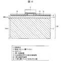
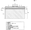
- FIG. 10 is a diagram schematically showing a cut surface of a light emitting device obtained by mounting the flip chip type LED chip 4 on the light emitting device substrate 20 ′.
- the difference from the light emitting device substrate 20 shown in FIG. 2 is that a copper paste is used to form the wiring pattern 3 ′ including the electrode terminal portion, and that the sprayed alumina layer (first 1 insulating layer 11) is covered with a smoothing layer 21 made of an alumina-containing glass layer.
- the surface of the alumina layer (first insulating layer 11) formed by thermal spraying is formed in a concavo-convex shape, and the surface of the alumina layer (first insulating layer 11) formed in this concavo-convex shape is used as an alumina-containing glass layer.
- the surface is covered with a smoothing layer 21 and filled with irregularities on the surface of the alumina layer (first insulating layer 11) to form a flat surface.
- FIG. 17 is a diagram for explaining a modification of the light emitting device substrate 20 ′ of the fifth embodiment.
- a buffer layer 250 is formed between the metal base 2 and the first insulating layer 11 as shown in FIG. .
- the first insulating layer 11 is formed on a base made of metal such as an aluminum plate to form a light emitting device substrate, particularly when this is used as a high output light emitting device substrate.
- the base made of the metal repeatedly expands and contracts.
- the first insulating layer 11 formed on the base body is subjected to a mechanical load due to a difference in coefficient of linear expansion coefficient with the metal base body, and there is a possibility that the peeling and the withstand voltage resistance may be reduced.
- the light-emitting element itself placed on the substrate may be affected by a thermal history due to a difference in coefficient of linear expansion coefficient with the metal substrate, and the life may be shortened. Therefore, in the modification of the fifth embodiment, the buffer layer 250 is formed between the metal base 2 and the first insulating layer 11 as shown in FIG.
- the metal substrate 2 is a substrate made of a material having high thermal conductivity.
- the material of the metal substrate 2 is not particularly limited as long as it has a high thermal conductivity.
- a substrate made of a metal containing aluminum, copper, stainless steel, or iron as a material can be used.
- the buffer layer 250 is the same as the buffer layer described in the first and second modifications of the first embodiment, and the buffer layer 250 has been described in the first and second modifications of the first embodiment, and is omitted here.
- the calculation model is simplified as long as the essence is not lost.
- FIGS. 1-10 Schematic diagrams of each light emitting device used for the estimation of the thermal resistance of the substrate for the light emitting device are shown in FIGS.
- FIG. 5 is a diagram schematically showing a cut surface of a light emitting device in which a protective film made of alumite is formed on the surface facing the formed surface, and further thermally connected to the heat sink via heat radiating grease.
- the substrate for a light-emitting device shown in FIG. 11A has a sprayed alumina layer (first insulating layer) made of alumina having a layer thickness of 300 ⁇ m formed by spraying on aluminum (metal substrate) having a thickness of 3 mm, and spraying.
- first insulating layer made of alumina having a layer thickness of 300 ⁇ m formed by spraying on aluminum (metal substrate) having a thickness of 3 mm, and spraying.
- an LED chip (light emitting element) having a planar dimension of 1000 ⁇ m in length ⁇ 1000 ⁇ m in width as a heat source is provided.
- glass or resin containing light-reflective ceramics is used for the ceramic-containing glass-based reflective layer (second insulating layer having light reflectivity). Glass or resin has a higher thermal conductivity than metal. Is two orders of magnitude lower, so the contribution to heat dissipation is negligibly small.
- the back surface of aluminum (metal substrate) in the light emitting device substrate shown in FIG. 11A is covered with a protective film made of alumite having a film thickness of 10 ⁇ m.
- the LED chip (light emitting element) mounted on the thermal spray electrode layer (terminal portion) is a flip chip type light emitting element, and therefore, below the LED chip (light emitting element) illustrated in FIG. Since the active layer is in the vicinity of the spray electrode layer (terminal portion), the heat dissipation is excellent, and the temperature rise in the LED chip can be almost ignored.
- the sprayed electrode layer (terminal part) is divided into positive and negative electrodes.
- a typical example of the sprayed electrode layer (terminal portion) is 1000 ⁇ m long ⁇ 400 ⁇ m wide with respect to the positive and negative electrodes of the light emitting element. It is appropriate to dispose positive and negative terminal portions each having a planar dimension of 2 mm. At this time, a spacing portion having a width of 200 ⁇ m is formed between the positive and negative terminal portions. As a result, the total plane dimension of the entire positive and negative terminal portion is 1000 ⁇ m long ⁇ 800 ⁇ m wide.
- the thermal resistance was calculated when a heating element having the same size as the LED chip (light emitting element) was placed on the sprayed electrode layer (terminal portion) having the same planar dimensions as the LED chip (light emitting element).
- the planar size of the LED chip (light emitting element) is 1000 ⁇ m square
- the planar size of the sprayed electrode layer (terminal portion) is also 1000 ⁇ m square.
- such a light-emitting device substrate is further thermally connected to the heat sink via heat radiation grease (thickness 50 ⁇ m).
- heat radiation grease thickness 50 ⁇ m.
- FIG. 13 (a) is a diagram schematically showing a cut surface of a light emitting device in which a flip chip type LED chip (light emitting element) is mounted on the light emitting device substrate 20 'shown in FIG.
- the difference between the light emitting device substrate shown in FIG. 13 (a) and the light emitting device substrate shown in FIG. 11 (a) is that copper metal is used for the formation of terminal portions and wiring patterns (formation of electrode layers). That is, the paste is used and the sprayed alumina layer (first insulating layer) is covered with an alumina-containing glass layer (smoothing layer).
- the metal paste By filling the irregularities formed on the surface of the sprayed alumina layer (first insulating layer) formed by thermal spraying into a flat surface, the metal paste can be printed stably and accurately.
- the case where all of the wiring pattern and the terminal portion for mounting the light emitting element are formed of a metal paste is taken as an example, but the metal paste and plating may be used for both.
- FIG. 12A (Comparative Example 1) is given as a comparative example of the configuration illustrated in FIG. 11A, and is formed by thermal spraying in the configuration illustrated in FIG. This corresponds to the case where the alumina layer (first insulating layer) is replaced with an alumina-containing glass layer.
- a copper metal paste is used to form an electrode layer including a wiring pattern and a terminal portion.
- FIG. 14A and FIG. 15A are diagrams schematically showing a cut surface of a light-emitting device in which a face-up LED chip (light-emitting element) is mounted on a light-emitting device substrate as a comparative example. .
- the thermal conductivity is generally as low as 1 W / (m ⁇ ° C.).
- a wiring pattern is further formed on the ceramic-containing glass-based reflective layer / insulator layer.
- the wiring pattern is electrically connected to the face-up LED chip (light-emitting element) with a gold wire or the like, and the face-up LED chip (light-emitting element) is supplied with electric power from the external power supply via the wiring pattern. Emits light.
- the back surface of aluminum (metal substrate) is covered with a protective film made of alumite having a thickness of 10 ⁇ m.
- the face-up type LED chip (light emitting element) is mounted on the ceramic-containing glass-based reflective layer / insulator layer using a die bond paste.
- the thickness of the die bond paste is usually very thin, about 5 ⁇ m, but the thermal conductivity is very low at about 0.2 W / (m ⁇ ° C), and when using a face-up LED chip (light emitting device) This thermal design cannot be ignored.
- the active layer of the face-up type LED chip (light-emitting element) is located on the upper side of the face-up type LED chip (light-emitting element) shown in FIG. The temperature rise of the active layer is not negligible.
- the planar dimension of the face-up type LED chip (light emitting element) is 1000 ⁇ m square, and the height of the active layer is 100 ⁇ m.
- the terminal portion of the electrode layer comes directly under the LED chip (light emitting element), but the face up type LED chip (light emitting element).
- the electrode on the wiring pattern
- Both face-up type LED chips (light-emitting elements) and wiring patterns are often formed on a ceramic-containing glass-based reflective / insulator layer.
- FIG. Such a light emitting device substrate is thermally connected to the heat sink via heat radiating grease, as in FIG.
- the substrate for a light emitting device as Comparative Example 3 shown in FIG. 15A is divided into two layers of the ceramic-containing glass-based reflective layer / insulator layer in Comparative Example 2 shown in FIG. Is an improvement.
- Highly reflective ceramic-containing glass-based reflective layer (low thermal conductivity) is used for the upper layer
- ceramic-containing glass-based thermal conductive layer (low thermal conductivity improved product) with high thermal conductivity is used for the lower layer.
- An insulating layer with high heat dissipation is realized while maintaining light reflectivity.
- the following calculation model is simplified as long as the essence is not lost in order to make it easy to estimate the thermal resistance of the light emitting device substrate.
- the simplification of electrode separation in the light emitting element mounting portion that is, the division of the pattern of the positive electrode and the negative electrode is not considered, and the thermal resistance is estimated as an integrated one. Such simplification is performed in the configuration shown in FIGS. 11A, 12A, and 13A.
- the unevenness due to the blasting treatment of aluminum (metal substrate) and the unevenness of the surface of the sprayed alumina layer (first insulating layer) are simplified as a flat surface.
- the unevenness due to the blasting treatment of aluminum is simplified as a flat surface, and the unevenness on the surface of the sprayed alumina layer (first insulating layer) is simplified to alumina.
- the location smoothed using the glass-containing layer (smoothing layer) is also simplified with the boundary between the sprayed alumina layer (first insulating layer) and the glass-containing alumina layer (smoothing layer) as a flat surface.
- the overall calculation is simplified and calculated.
- the thermal resistance Rth (° C./W) and the temperature rise ⁇ T (° C.) in each layer obtained by calculation are similarly shown in FIGS. 11 (b) to 15 (b).
- the thermal resistance of the light emitting device substrate is obtained as a subtotal by adding the thermal resistance Rth (° C./W) in each layer.
- the thermal resistance of the entire light emitting device is shown in the total part.
- the temperature rise in the light emitting element is included in the calculation of the thermal resistance of the entire light emitting device. Is also included in the calculation.
- the flip chip type LED chip since the flip chip type LED chip (light emitting element) is used, the active layer is in the vicinity of the light emitting device substrate, and the temperature rise in the LED chip is ignored. I omitted it as possible.
- the thermal resistance per light emitting element is obtained considering only the heat generated by the light emitting element having a dimension of 1000 ⁇ m square.
- the calculation result of the temperature rise ⁇ T was assumed to assume that 0.75 W of 50% was lost as heat with respect to the input power of 1.5 W per light emitting element.
- the thermal resistance Rth (° C./W) of each layer is calculated assuming that the active layer of the light emitting element is the only heat source. Furthermore, in FIG. 11 (b), FIG. 12 (b), FIG. 13 (b), FIG. 14 (b) and FIG. 15 (b), not only the thermal resistance Rth (° C./W) of each layer, The temperature rise ⁇ T (° C.) is also obtained. This temperature rise ⁇ T (° C.) is a value when the heat generation amount of the heat source is assumed to be 0.75 W.
- the spread of heat in the lateral direction is taken into consideration. Specifically, as shown by the broken lines in FIGS. 11A, 12A, 13A, 14A, and 15A, the light emitting device substrate extends in the vertical direction. On the other hand, it was determined on the assumption that heat is uniformly diffused in the 45 ° direction.
- the terminal portion of the electrode layer is covered with a ceramic-containing glass-based reflective layer having a low thermal conductivity, and the thermal conductivity of the terminal portion of the electrode layer is one to two digits higher than the surroundings,
- it is sufficient to calculate that heat passes only through the terminal portion of the electrode layer and it is sufficient to consider the heat spread in the lateral direction in the layer below the electrode pattern located below.
- the thermal resistance of the light-emitting device substrate is estimated.
- the light emitting device substrate shown in the schematic diagram of FIG. 11A is about 11 ° C./W
- the light emitting device substrate shown in the schematic diagram of FIG. 12A is about 35 ° C./W
- the light emitting device substrate shown in the figure is about 22 ° C./W
- the light emitting device substrate shown in the schematic diagram of FIG. 14A is about 186 ° C./W
- the light emitting device substrate shown in the schematic diagram of FIG. about 103 ° C./W.
- the thickness of the insulating layer up to the electrode layer or the thickness of the electrical insulating layer up to the LED chip (light emitting element) is set. Comparison is made uniformly at 300 ⁇ m.
- the insulating layer having a thickness of 300 ⁇ m is all the reflective layer.
- This reflective layer is a zirconia-containing glass-based insulating layer formed by sintering a sol-gel glass containing zirconia as a ceramic material.
- the thermal conductivity ⁇ th of this reflective layer is 1 W / (m ⁇ ° C.). is there.
- the insulating layer in the light emitting device substrate shown in FIG. 15A has a laminated structure of a reflective layer and a heat conductive layer having low thermal conductivity.
- the reflective layer placed on the surface layer has a thickness of 100 ⁇ m and is a zirconia-containing glass-based insulating layer
- the heat conductive layer has a thickness of 200 ⁇ m and has a thermal conductivity higher than that of the reflective layer. It is a high alumina-containing glass-based insulating layer.
- the heat conductive layer is formed by sintering sol-gel glass in a state containing alumina particles.
- the thermal conductivity ⁇ th of the thermal conductive layer is 5 W / (m ⁇ ° C.).
- the insulating layer (first insulating layer) of the light emitting device substrate shown in FIG. 11A is a sprayed alumina layer (ceramic layer) formed by high-speed flame spraying (HVOF) or plasma spraying.
- This insulating layer (first insulating layer) is formed with a thickness of 300 ⁇ m under the thermal spray electrode layer composed of the wiring pattern and the terminal portion.
- the thermal conductivity ⁇ th of this insulating layer (first insulating layer) is 15 W / (m ⁇ ° C.).
- the ceramic-containing glass-based reflective layer (second insulating layer having light reflectivity) is formed so as to cover the insulating layer (first insulating layer) and the wiring pattern, and is illustrated by a broken line in FIG. ing.
- the thermal conductivity of the ceramic-containing glass-based reflective layer is the thermal conductivity of the reflective layer of the light emitting device substrate shown in FIGS. 14 (a) and 15 (a).
- the thermal conductivity ⁇ th is 1 W / (m ⁇ ° C.).
- the thermal conductivity is low, as is intuitively understood from FIGS. 11 (a), 12 (a), and 13 (a), the main heat dissipation path does not include the second insulating layer having the light reflectivity. Therefore, the influence on the thermal resistance can be ignored.
- the sprayed alumina layer which is the insulating layer (first insulating layer) of the light emitting device substrate illustrated in FIG. 11A and the ceramic-containing glass-based heat conductive layer of the light emitting device substrate illustrated in FIG.
- some alumina-containing glass contains alumina as a material
- the ceramic-containing glass-based heat conductive layer illustrated in FIG. 15A is affected by glass having low thermal conductivity because glass is used as a binder. Therefore, it is considered that the thermal conductivity ⁇ th of this thermal conductive layer is as low as 5 W / (m ⁇ ° C.).
- an insulating layer (first insulating layer) is formed by thermal spraying.
- alumina as a ceramic is deposited as it is on the insulating layer (first insulating layer). Therefore, the thermal conductivity ⁇ th of the insulating layer (first insulating layer) is considered to be a high value of 15 W / (m ⁇ ° C.).
- the electrode layer composed of the wiring pattern and the terminal portion is formed by further laminating a copper conductive layer laminated by high-speed flame spraying (HVOF) or plasma spraying using chemical etching or dry etching.
- HVOF high-speed flame spraying
- the wiring pattern has a thickness of 100 ⁇ m
- the protruding terminal portion formed for mounting the LED chip (light emitting element) has a thickness of 200 ⁇ m
- the thermal conductivity ⁇ th is 200 W / (m ⁇ ° C.).
- the thermal conductivity of pure copper is approximately 400 W / (m ⁇ ° C.)
- the copper electrode layer formed by thermal spraying is partially oxidized at the time of formation, and the thermal conductivity is lower than that of pure copper. .
- the degree of oxidation is high, the thermal conductivity is lower than 200 W / (m ⁇ ° C.), and conversely increases if the degree of oxidation is mild.
- the electrode layer may be formed by a cold spray method, which is a method of thermal spraying. In this case, the thermal conductivity is higher than 200 W / (m ⁇ ° C.), and the heat dissipation is good. Get better.
- the copper electrode layer formed by thermal spraying as described above is, for example, 100 to 200 W / (m ⁇ ° C.) and sufficiently high heat conduction, although it is inferior to pure copper due to partial oxidation. Rate can be realized.
- the thermal conductivity of the copper electrode layer formed of the metal paste has a low thermal conductivity of about an order of magnitude, showing only a thermal conductivity of about 10 to 30 W / (m ⁇ ° C.) at most.
- the electrode layer formed by thermal spraying is formed only by metal
- the electrode layer formed by metal paste is obtained by drying and baking agglomerated metal fine particles using an organic substance such as a resin as a binder.
- the contact resistance at the grain boundary between the fine particles is high, and as a result, the thermal conductivity seen in the entire electrode layer is lowered.
- the alumina-containing glass layer that is the insulating layer of the light emitting device substrate illustrated in FIG. 12A has a thickness of 300 ⁇ m, and among the ceramic-containing glass-based insulating layers, the alumina-containing glass insulating layer has a high thermal conductivity. is there.
- the alumina-containing glass layer has a thermal conductivity ⁇ th of 5 W / (m ⁇ ° C.).
- the alumina-containing glass layer is made of the same material as the alumina-containing glass layer used for the heat conductive layer in FIG. Although it repeats, since glass is used as a binder, it is influenced by the glass with low thermal conductivity, and it is thought that it becomes a value lower than the alumina layer formed by thermal spraying.
- the electrode layer composed of the wiring pattern and the terminal portion is a copper electrode layer formed by printing, drying and sintering a metal paste.
- the thermal conductivity ⁇ th is 30 W / (m ⁇ ° C.).
- the electrode layers are all made of a metal paste here.
- the electrode layer is an electrode layer whose surface is covered with plating using the metal paste as a base electrode pattern. Also good.
- the thermal resistance of the electrode layer in this case is determined by the plating material used and the laminated structure.
- the thickness of the electrode layer is the same as that of the substrate for a light emitting device shown in FIG. 11A, the thickness of the wiring pattern is 100 ⁇ m, and the thickness of the protruding terminal portion formed for mounting the LED chip (light emitting element). 200 ⁇ m.
- the ceramic-containing glass-based reflective layer is formed so as to cover the alumina-containing glass layer, which is an insulating layer, and the wiring pattern in the same manner as in FIG. 11A, and is also illustrated by a broken line in FIG.
- the same zirconia-containing glass-based insulator is used as the material, and the thermal conductivity ⁇ th is 1 W / (m ⁇ ° C.).
- this reflective layer is not included in the main heat dissipation path, and therefore the influence on the thermal resistance can be ignored.
- the difference between the light emitting device substrate shown in FIG. 13A and the light emitting device substrate shown in FIG. 11A will be described.
- the insulating layer of the light emitting device substrate shown in FIG. 13A is a sprayed alumina layer (first insulating layer) formed by high-speed flame spraying (HVOF) or plasma spraying, as in FIG. 11A. is there.
- the surface of this sprayed alumina layer (first insulating layer) is covered with an alumina-containing glass layer (smoothing layer) to form a flat surface, and then a metal (copper) paste is printed, dried and sintered.
- a copper electrode layer is formed.
- the alumina-containing glass layer was formed by sintering sol-gel glass containing alumina particles.
- the thermal conductivity ⁇ th of the alumina-containing glass layer (smoothing layer) that is the insulating layer is 5 W / (m ⁇ ° C.).
- alumina-containing glass layer which is an insulating layer
- a flat surface may be formed by coating with a glass-based insulator layer obtained by sintering only sol / gel glass without adding ceramic particles. In this case, the thermal conductivity is reduced to about 1 W / (m ⁇ ° C.).
- a glass-based insulator layer containing ceramic particles other than alumina particles may be formed.
- the electrode layer illustrated in FIG. 13A has a wiring pattern thickness of 100 ⁇ m and a protruding terminal portion formed to mount an LED chip (light emitting element) has a thickness of 200 ⁇ m, as in FIG. did.
- the electrode layer is formed of a copper metal paste, the thermal conductivity ⁇ th is 30 W / (m ⁇ ° C.).
- an electrode layer having a metal paste as a base electrode pattern and a surface coated with plating may be used in the actual case.
- the electrode layer is formed of a copper metal paste.
- the above-mentioned uneven surface is an alumina-containing glass layer (smoothing) that is an insulating layer.
- the boundary surface between the sprayed alumina layer (first insulating layer) and the alumina-containing glass layer (smoothing layer) covering it Is a plane like other boundary surfaces.
- the thickness of the alumina-containing glass layer (smoothing layer) is 50 ⁇ m and constant.
- a thermal spraying alumina layer first insulating layer formed by thermal spraying having a thermal conductivity ⁇ th of 15 W / (m ⁇ ° C.) and a metal paste.
- an alumina-containing glass layer thermal conductivity ⁇ th, 5 W / (m ⁇ C)
- the result of the trial calculation of the thermal resistance of the light emitting device substrate performed under the premise as described above is about 11 ° C./in the case of the light emitting device substrate shown in the schematic diagram of FIG. W, which is about 35 ° C./W for the light emitting device substrate shown in the schematic diagram of FIG. 12A, and about 22 ° C./W for the light emitting device substrate shown in the schematic diagram of FIG.
- the light emitting device substrate shown in the schematic diagram of FIG. 14A has a temperature of about 186 ° C./W
- the light emitting device substrate shown in the schematic diagram of FIG. 15A has a temperature of about 103 ° C./W.
- the main part that determines the thermal resistance is an insulating layer and an electrode layer disposed between the light emitting element and aluminum (metal substrate).
- the contribution from aluminum (metal substrate) and alumite (protective film) is less than 10% at the maximum even in FIGS. 11 (b), 12 (b), and 13 (b).
- the advantage of using a dense and high-quality ceramic layer on the metal substrate is an improvement in long-term reliability in addition to heat dissipation and dielectric strength.
- the ceramic layer functions as a buffer layer that fills the difference in linear expansion coefficient between the light emitting element and the metal substrate, and the life of the flip chip type light emitting element can be improved.
- the lifespan of the light emitting element can be prevented by interposing a thick ceramic layer made of alumina between the metal substrate and the light emitting element.
- sapphire, aluminum nitride, or the like is used as a base substrate of a blue light emitting element or a green light emitting element
- silicone (Si) is used as a base substrate of a red light emitting element.
- the difference in coefficient of linear expansion between the ceramic layer and the base substrate of the light emitting element, sapphire, aluminum nitride, and silicone is small.
- the expansion coefficients agree.
- a dense and high-quality ceramic layer such as that formed by thermal spraying is interposed on a metal substrate, especially when a thick film is formed, the ceramic layer absorbs expansion and contraction of the metal substrate, and a flip-chip type light emitting device
- the expansion and contraction load caused by the metal substrate is not transmitted to As a result, the lifetime reduction due to external expansion and contraction does not occur in the light emitting element, and long-term reliability of the light emitting device can be ensured.
- the thermal conductivity of the ceramic layer formed by thermal spraying is higher than the thermal conductivity of the ceramic layer using the binder, and the heat dissipation is not lowered even if it is a thick film in order to achieve the above object.
- the substrate for a light-emitting device is a substrate for a light-emitting device provided with a base made of a metal material, and includes a first insulating layer having thermal conductivity formed on one surface of the base.
- the wiring pattern is preferably formed by patterning a metal conductive layer formed by thermal spraying.
- the wiring pattern is formed by patterning a metal conductive layer formed by thermal spraying, the adhesion between the first insulating layer and the wiring pattern is good, and heat is applied between them. Since a high resistance layer having low conductivity is not interposed, a light emitting device substrate having good heat dissipation can be realized. In addition, since the wiring pattern is finally removed from the conductive layer by etching after the conductive layer is formed, there is no formation failure of the wiring pattern or short circuit between the electrode terminals in the light emitting element mounting portion of the wiring pattern. .
- a third insulating layer as a planarizing layer is provided between the first insulating layer and the wiring pattern. Preferably it is formed.
- the ground surface is a flat surface. Can be formed.
- the second insulating layer is preferably a layer made of a mixture of at least one of glass and resin and ceramics. .
- the second insulating layer is a layer made of a mixture of at least one of glass and resin and ceramics, the second insulating layer can be formed at a relatively low temperature.
- the thermal conductivity of the first insulating layer is higher than the thermal conductivity of the second insulating layer.
- the light reflecting performance of the second insulating layer is higher than the light reflecting performance of the first insulating layer.
- the thermal conductivity of the first insulating layer formed on the base made of the metal material is high, a light emitting device substrate having excellent heat dissipation can be realized.
- the substrate for a light emitting device according to aspect 6 of the present invention, in addition to the above aspects 1 to 5, the substrate is preferably made of any metal material of aluminum and copper.
- the base is formed of aluminum or copper having a relatively high thermal conductivity, a light emitting device substrate having excellent heat dissipation can be realized.
- a protective layer is formed on at least a part or all of the region where the first insulating layer is not formed in the base. It is preferable that
- the protective layer may be an anodized aluminum film (alumite layer).
- alumite layer an anodized aluminum film (alumite layer)
- the wiring pattern is preferably made of copper or silver.
- an adhesive layer may be formed between the base and the first insulating layer.
- a metal thin plate can be used for the conductive layer, and the step of forming the conductive layer can be omitted. Further, the wiring pattern can be cut out from the conductive layer made of the metal thin plate by etching. If a flat plate is used for the metal thin plate, the step of smoothing the metal conductive layer performed before the etching process for forming the wiring pattern can be omitted. In addition, the formation failure of the wiring pattern and the short circuit between the electrode terminals in the light emitting element mounting portion of the wiring pattern do not occur. Furthermore, since a metal with high purity can be used for the metal thin plate, a wiring pattern having high thermal conductivity and high electrical conductivity can be formed.
- the first insulating layer can be formed directly on the conductive layer without inserting an adhesive layer between the conductive layer made of a thin metal plate and the first insulating layer. Adhesiveness with the wiring pattern formed from the conductive layer is good, and a high resistance layer with low thermal conductivity is not interposed between the two layers, realizing a light-emitting device substrate with good heat dissipation it can.
- the thickness of the first insulating layer is 50 ⁇ m or more and 500 ⁇ m or less.
- the thickness is preferably 10 ⁇ m or more and 500 ⁇ m or less.
- the inside of the second insulating layer may be further constituted of a plurality of layers as appropriate.
- a layer having high thermal conductivity can be disposed in the second insulating layer close to the first insulating layer, and a layer having high light reflectance can be disposed in the opposite layer. It is possible to realize a light emitting device substrate having long-term reliability including reflectance, high heat dissipation, dielectric strength, heat resistance and light resistance. However, the levels of thermal conductivity and light reflectance referred to here are relative comparisons in the second insulating layer.
- the first insulating layer is an insulating layer made of alumina
- the second insulating layer is made of zirconia or titanium oxide.
- an insulating layer in which particulate ceramics containing at least one of alumina and aluminum nitride is covered with vitreous may be used.
- the first insulating layer is an insulating layer made of alumina
- the second insulating layer is made of zirconia or titanium oxide.
- a resin containing at least one of alumina and aluminum nitride as particulate ceramics, and the resin may be a silicone resin, an epoxy resin, or a fluororesin.
- silicone resin, epoxy resin, or fluororesin is inferior to vitreous in terms of heat resistance and light resistance, but has an advantage that the curing process is low and the forming process is easy.
- a buffer layer made of a substance having a smaller linear expansion coefficient than the base is provided between the base and the first insulating layer. It may be formed.
- a first insulating layer is formed on a base made of metal such as an aluminum plate to form a substrate for a light-emitting device, particularly when this is used as a substrate for a light-emitting device with high output, it is placed on the substrate.
- the base made of metal repeatedly expands and contracts.
- the first insulating layer formed on the substrate is subjected to a mechanical load due to a difference in coefficient of linear expansion coefficient with the substrate, and there is a possibility that peeling and dielectric strength are reduced.
- the light emitting element itself placed on the base body may be affected by the thermal history due to a difference in coefficient of linear expansion coefficient with the base body, and the life may be shortened.
- a buffer layer made of a material having a smaller linear expansion coefficient than that of the base is formed between the base and the first insulating layer.
- a buffer layer 250 made of a material having a linear expansion coefficient smaller than that of the substrate and larger than that of the first insulating layer may be formed.
- a light-emitting device includes a light-emitting element that is electrically connected to a terminal portion of the wiring pattern exposed from the second insulating layer in the light-emitting device substrate according to any one of aspects 1 to 14, and the wiring pattern Are connected to an external wiring or an external device, and are formed of a light-reflective resin frame portion that surrounds a region where the light emitting element is disposed on the light emitting device substrate, and the frame portion. And a sealing resin that seals a region surrounded by is formed.
- the sealing resin may contain a phosphor.
- the light emitting element may be electrically connected to the terminal portion of the wiring pattern by flip chip bonding.
- a light emitting device including a flip chip type light emitting element can be realized.
- a method for manufacturing a substrate for a light emitting device is a method for manufacturing a substrate for a light emitting device including a base made of a metal material, wherein the first surface having thermal conductivity on one surface of the base.
- a method for manufacturing a substrate for a light-emitting device that combines high reflectivity, high heat dissipation, dielectric strength, long-term reliability including heat resistance and light resistance, and excellent mass productivity is realized. it can.
- the first insulating layer may be formed by spraying alumina as the ceramic.
- the first insulating layer made of alumina having a high balance between insulation and thermal conductivity can be formed by thermal spraying.
- particulate ceramics containing at least one of zirconia, titanium oxide, alumina, and aluminum nitride are formed by a sol-gel reaction of a glass raw material.
- the second insulating layer covered with the vitreous material may be formed.
- the second insulating layer can be formed at a relatively low temperature by a sol-gel reaction.
- the particulate ceramic containing at least one of zirconia, titanium oxide, alumina, and aluminum nitride is obtained by melting and hardening glass particles.
- the second insulating layer covered with the formed glassy material may be formed.
- the second insulating layer having high reflectivity and insulating layer can be formed.
- the resin containing at least one of zirconia, titanium oxide, alumina, and aluminum nitride is formed as a particulate ceramic.
- a second insulating layer is formed, and the resin may be a silicone resin, an epoxy resin, or a fluororesin.
- the second insulating layer can be formed relatively easily because its curing temperature is low.
- the conductive layer may be formed by spraying metal.
- the conductive layer can be formed at a relatively low temperature.
- a protective layer is formed on at least a part or all of the region where the first insulating layer is not formed on the base.
- the protective layer may be an anodized aluminum film (alumite layer).
- alumite layer an anodized aluminum film (alumite layer)
- the protective layer formed by the above manufacturing method it is possible to suppress the substrate from being damaged after the post process or after the product is completed, and the long-term reliability can be improved.
- the base body and the first insulating layer may be bonded together by an adhesive layer.
- the adhesive layer is formed, a metal thin plate can be used, and the step of forming the conductive layer can be omitted.
- the portion where the conductive layer is exposed is not only a terminal portion electrically connected to the light-emitting element, but also external wiring or
- the anode electrode (anode land) 7 and the cathode electrode (cathode land) 8 connected to an external device may also be exposed.
- the portion where the conductive layer is exposed is not only a terminal portion electrically connected to the light emitting element, but also an external wiring or
- a step of forming a third insulating layer as a planarizing layer between the first insulating layer and the conductive layer is preferably included.
- the conductive layer can be stably and accurately provided. Can be formed.
- the present invention can be suitably used for a light emitting device substrate, a light emitting device using the light emitting device substrate, and a manufacturing method for manufacturing the light emitting device substrate.
- SYMBOLS 1 Light-emitting device 2 Metal substrate 3 Wiring pattern 3 'Wiring pattern (copper paste) 4 LED chip (light emitting element) 5 Light Reflecting Resin Frame 6 Phosphor-Containing Sealing Resin 7 Anode Electrode (Anode Land) 8 Cathode electrode (cathode land) 9 Anode mark 10 Cathode mark 11 First insulating layer (protective layer) having thermal conductivity DESCRIPTION OF SYMBOLS 12 2nd insulating layer which has light reflectivity 13 Resist 14 Back surface protection sheet 15 Resist 16 Adhesive layer 17 Resist 18 Resist 19 Protective film (protective layer) 20 Light Emitting Device Substrate 20 'Light Emitting Device Substrate 20a Light Emitting Device Substrate 21 Smoothing Layer (Third Insulating Layer) 250 Buffer layer
Landscapes
- Engineering & Computer Science (AREA)
- Microelectronics & Electronic Packaging (AREA)
- Chemical & Material Sciences (AREA)
- Inorganic Chemistry (AREA)
- Led Device Packages (AREA)
- Ceramic Engineering (AREA)
- Insulated Metal Substrates For Printed Circuits (AREA)
Abstract
Description
(セラミックス基板)
例えば、セラミックス基板は、板状のセラミックス基板に電極パターンを形成して作製される。発光装置の高出力化傾向に伴って、発光素子を多数並べて、明るさを向上させることが追及された結果、年々、セラミックス基板は大型化の一途をたどってきた。
(金属基体を用いた基板)
一方、このようなセラミックス基板での上記問題点を克服する目的で、高出力発光装置用基板として、熱伝導性の高い金属基体を使用する場合がある。ここで、金属基体上に発光素子を搭載するためには、電極パターンを形成するためにも金属基体上に絶縁層を設けなくてはならない。
本発明の一実施形態について図1~図4に基づいて説明すれば、以下のとおりである。(発光装置)
図1は、本実施の形態の発光装置1の概略構成を示す平面図である。
以下、図2に基づいて、発光装置用基板20に備えられた各層について説明する。
本実施の形態においては、金属材料からなる基体2としてアルミニウム基体を用いた。アルミニウム基体としては、例えば、縦50mm×横50mm×厚み3mmのアルミニウム板を用いることができる。アルミニウムの長所として、軽量で加工性に優れ、熱伝導率が高いことが挙げられる。また、アルミニウム基体には陽極酸化処理を妨げない程度のアルミニウム以外の成分が含まれていてもよい。なお、詳しくは後述するが、本実施の形態においては、比較的低い温度で、基体2上に、第1の絶縁層11と、配線パターン3と、光反射性を有する第2の絶縁層12と、を形成することができるので、金属材料からなる基体2として660℃の融点を有する低融点金属であるアルミニウム基体を用いることができる。このような理由から、アルミニウム基体に限定されることはなく、例えば、銅基体など金属材料からなる基体2として選択できる材質の幅が広い。
本実施の形態においては、図2に図示されているように、発光装置用基板20に高放熱性と、高い絶縁耐圧特性とを安定的に付与するために、熱伝導性のセラミックス絶縁体である第1の絶縁層11が、金属材料からなる基体2と、配線パターン3または光反射性を有する第2の絶縁層12との間に形成されている。
溶射(Thermal Spraying)とは、溶融あるいはそれに近い状態に加熱した溶射材料から得られる溶融粒子を、基体面に高速で衝突させ、積層させる方法であり、溶射材料は、粉末あるいは線材の形態で溶射装置に供給される。溶射においては、溶射材料を加熱する方法により、フレーム溶射、アーク溶射、プラズマ溶射、高速フレーム溶射などに分類される。材料を溶融させること無く不活性ガスと共に超音速流で固相状態のまま基材に衝突させて被膜を形成するコールドスプレー方式も溶射の一種に分類される。なお、セラミックス層を金属基体上に形成する目的としては、高速フレーム溶射、プラズマ溶射、フレーム溶射が適当である。以下、高速フレーム溶射、プラズマ溶射およびフレーム溶射について説明する。
第1の絶縁層11上に形成する配線パターン3は、従来の配線パターンの形成方法で形成することもできるが、従来の配線パターンの形成方法を用いた場合、配線パターンは、電極下地用の金属ペーストとメッキ層とで構成され、例えば、電極下地用の金属ペーストでは、バインダーとして樹脂等の有機物を使用しているため熱伝導率が低く、熱抵抗が高くなる一因となっていた。
図2に図示されているように、発光装置用基板20においては、配線パターン3の一部が露出するように、第1の絶縁層11の上および配線パターン3の一部の上に光反射性を有する第2の絶縁層12が形成されている。
図2では、LEDチップ4が、発光装置用基板20に搭載され、パッケージ化されている。ここでは、LEDチップ4が、フリップチップボンディングにより、配線パターン3の端子部分と電気的に接続されている。
以下、図3および図4に基づいて、発光装置用基板20の製造工程について説明する。
本発明の実施の形態1の変形例について、図16に基づいて説明すれば、以下のとおりである。図16は図2に示した実施の形態1の発光装置用基板20の変形例を説明する図である。
上記変形例1では、緩衝層250を金属あるいは合金層としているが、本発明はこれに限定されるものではなく、代わりにシート状に加工した樹脂やペースト状の樹脂を用いて緩衝層250としてもよい。
次に、図5、図6および図7に基づいて、本実施の形態2について説明する。本実施の形態において説明する発光装置用基板20aは、金属基体2と第1の絶縁層11との間に接着層16が備えられている点において実施の形態1で説明した発光装置用基板20とは異なる。なお、説明の便宜上、上記実施の形態1の図面に示した部材と同じ機能を有する部材については、同じ符号を付し、その説明を省略する。
以下、図6および図7に基づいて、発光装置用基板20aの製造工程について説明する。
次に、図8に基づいて、本実施の形態3について説明する。本実施の形態において説明する発光装置用基板は、保護膜(保護層)として第1の絶縁層11を金属基体の側面にも形成している点において実施の形態1および2で説明した発光装置用基板とは異なる。なお、説明の便宜上、上記実施の形態1および2の図面に示した部材と同じ機能を有する部材については、同じ符号を付し、その説明を省略する。
次に、図9に基づいて、本実施の形態4について説明する。本実施の形態において説明する発光装置用基板は、保護膜19(保護層)を金属基体2の側面のみでなく、第1の絶縁層11が形成されている面と対向する面(金属基体2の裏面)にも形成し、裏面保護シート14を使用しないという点において実施の形態1から3で説明した発光装置用基板とは異なる。なお、説明の便宜上、上記実施の形態1から3の図面に示した部材と同じ機能を有する部材については、同じ符号を付し、その説明を省略する。
次に、図10に基づいて、本実施の形態5について説明する。本実施の形態において説明する発光装置用基板20′においては、配線パターン3′の形成に金属ペーストである銅ペーストを用いていることと、溶射アルミナ層(第1の絶縁層11)がアルミナ含有ガラス層である平滑化層21(第3の絶縁層)で被覆されている点において実施の形態1から4で説明した発光装置用基板とは異なる。なお、説明の便宜上、上記実施の形態1から4の図面に示した部材と同じ機能を有する部材については、同じ符号を付し、その説明を省略する。
本発明の実施形態5の変形例について、図17に基づいて説明すれば、以下のとおりである。図17は本実施の形態5の発光装置用基板20′の変形例を説明する図である。
本実施の形態においては、本発明の効果を確認するために、発光装置用基板の熱抵抗を試算し、比較例との比較を行った。
図11(a)は、図2に図示した発光装置用基板20上に、フリップチップ型発光素子であるLEDチップ4を搭載するとともに、発光装置用基板20の金属基体2においてLEDチップ4が設けられている面と対向する面にアルマイトからなる保護膜を形成し、さらには、ヒートシンクに放熱グリースを介して熱的に接続されている発光装置の切断面を模式的に示す図である。
図11(a)から図15(a)までの模式図で示した層構造を持つ発光装置用基板の熱抵抗を計算するために用いた、各層ごとの熱伝導率σth(W/(m・℃))と、層厚d(mm)は、図11(b)から図15(b)にそれぞれ示した。
発光装置用基板の熱抵抗の値は、熱源の位置や寸法に依存するが、図11(b)、図12(b)、図13(b)、図14(b)および図15(b)に示す熱抵抗Rth(℃/W)の結果においては、発光素子の活性層を唯一の熱源と仮定して、各層の熱抵抗Rth(℃/W)を計算している。さらに、図11(b)、図12(b)、図13(b)、図14(b)および図15(b)においては、各層の熱抵抗Rth(℃/W)だけでなく、各層の温度上昇ΔT(℃)も求めているが、この温度上昇ΔT(℃)は、熱源の発熱量を0.75Wと仮定した場合の値である。
図11の(b)に示した、各層の熱抵抗Rth(℃/W)および温度上昇ΔT(℃)は、上記計算方法で試算したものである。図12の(b)、図13の(b)、図14の(b)および図15の(b)においても、同様の計算方法で試算している。
実施の形態1から6のように、金属基体上に緻密で高品質なセラミックス層を用いる利点としては、放熱性、絶縁耐圧性以外にも、長期信頼性の改善が挙げられる。発光素子と金属基体の線膨張率の差を埋める緩衝層としてセラミックス層が機能し、フリップチップ型発光素子の寿命を改善できる。
本発明の態様1における発光装置用基板は、金属材料からなる基体を備えた発光装置用基板であって、上記基体の一方側の面に形成された熱伝導性を有する第1の絶縁層と、上記第1の絶縁層の上に形成された配線パターンと、上記配線パターンの一部が露出するように、上記第1の絶縁層の上および上記配線パターンの一部の上に形成された光反射性を有する第2の絶縁層と、を備え、上記第1の絶縁層は、溶射によって形成されたセラミックスからなる層であることを特徴としている。
2 金属基体
3 配線パターン
3′ 配線パターン(銅ペースト)
4 LEDチップ(発光素子)
5 光反射樹脂枠
6 蛍光体含有封止樹脂
7 アノード電極(アノードランド)
8 カソード電極(カソードランド)
9 アノードマーク
10 カソードマーク
11 熱伝導性を有する第1の絶縁層(保護層)
12 光反射性を有する第2の絶縁層
13 レジスト
14 裏面保護シート
15 レジスト
16 接着層
17 レジスト
18 レジスト
19 保護膜(保護層)
20 発光装置用基板
20′ 発光装置用基板
20a 発光装置用基板
21 平滑化層(第3の絶縁層)
250 緩衝層
Claims (6)
- 金属材料からなる基体を備えた発光装置用基板であって、
上記基体の一方側の面に形成された熱伝導性を有する第1の絶縁層と、
上記第1の絶縁層の上に形成された配線パターンと、
上記配線パターンの一部が露出するように、上記第1の絶縁層の上および上記配線パターンの一部の上に形成された光反射性を有する第2の絶縁層と、を備え、
上記第1の絶縁層は、溶射によって形成されたセラミックスからなる層であることを特徴とする発光装置用基板。 - 前記基体と前記第1の絶縁層の間に、前記基体よりも線膨脹率の小さい物質からなる緩衝層が形成されていることを特徴とする請求項1に記載の発光装置用基板。
- 上記配線パターンは、溶射によって形成された金属導電層をパターニングして形成されていることを特徴とする請求項1または2に記載の発光装置用基板。
- 上記基体において、上記第1の絶縁層が形成されていない領域の少なくとも一部または全部には、保護層が形成されていることを特徴とする請求項1から3の何れか1項に記載の発光装置用基板。
- 請求項1から4の何れか1項に記載の発光装置用基板における上記第2の絶縁層から露出した上記配線パターンの端子部分と電気的に接続する発光素子を備え、
上記配線パターンは、外部配線または外部装置に接続されており、
上記発光装置用基板における上記発光素子が配置されている領域を取り囲むように形成された光反射性を有する樹脂からなる枠部と、
上記枠部によって囲まれる領域を封止する封止樹脂とが形成されていることを特徴とする発光装置。 - 金属材料からなる基体を備えた発光装置用基板の製造方法であって、
上記基体の一方側の面に熱伝導性を有する第1の絶縁層と上記第1の絶縁層上に導電層とを形成する第1の工程と、
上記導電層の一部が露出するように、上記第1の絶縁層の上および上記導電層の一部の上に光反射性を有する第2の絶縁層を形成する第2の工程と、を含み、
上記第1の工程においては、溶射によりセラミックスからなる上記第1の絶縁層を形成することを特徴とする発光装置用基板の製造方法。
Priority Applications (3)
| Application Number | Priority Date | Filing Date | Title |
|---|---|---|---|
| CN201480072071.0A CN105874619B (zh) | 2014-01-10 | 2014-12-04 | 发光装置用基板、发光装置及发光装置用基板的制造方法 |
| US15/101,969 US9806244B2 (en) | 2014-01-10 | 2014-12-04 | Substrate for light emitting device, light emitting device, and manufacturing method of substrate for light emitting device |
| JP2015556735A JP6215360B2 (ja) | 2014-01-10 | 2014-12-04 | 発光装置用基板、発光装置および発光装置用基板の製造方法 |
Applications Claiming Priority (4)
| Application Number | Priority Date | Filing Date | Title |
|---|---|---|---|
| JP2014-003736 | 2014-01-10 | ||
| JP2014003736 | 2014-01-10 | ||
| JP2014089619 | 2014-04-23 | ||
| JP2014-089619 | 2014-04-23 |
Publications (1)
| Publication Number | Publication Date |
|---|---|
| WO2015104928A1 true WO2015104928A1 (ja) | 2015-07-16 |
Family
ID=53523766
Family Applications (1)
| Application Number | Title | Priority Date | Filing Date |
|---|---|---|---|
| PCT/JP2014/082158 Ceased WO2015104928A1 (ja) | 2014-01-10 | 2014-12-04 | 発光装置用基板、発光装置および発光装置用基板の製造方法 |
Country Status (4)
| Country | Link |
|---|---|
| US (1) | US9806244B2 (ja) |
| JP (1) | JP6215360B2 (ja) |
| CN (1) | CN105874619B (ja) |
| WO (1) | WO2015104928A1 (ja) |
Cited By (4)
| Publication number | Priority date | Publication date | Assignee | Title |
|---|---|---|---|---|
| JP2017195258A (ja) * | 2016-04-19 | 2017-10-26 | 市光工業株式会社 | 光源装置、移動体用発光装置 |
| WO2022065284A1 (ja) * | 2020-09-24 | 2022-03-31 | スタンレー電気株式会社 | 半導体発光装置及び半導体発光モジュール |
| JP2023506613A (ja) * | 2019-10-24 | 2023-02-17 | 京東方科技集團股▲ふん▼有限公司 | 駆動基板及びその製作方法並びに表示装置 |
| US12495652B2 (en) | 2020-12-10 | 2025-12-09 | Stanley Electric Co., Ltd. | Semiconductor light emitting device and supporting substrate for semiconductor light emitting elements |
Families Citing this family (17)
| Publication number | Priority date | Publication date | Assignee | Title |
|---|---|---|---|---|
| WO2015093170A1 (ja) * | 2013-12-18 | 2015-06-25 | シャープ株式会社 | 発光装置用基板、発光装置、及び、発光装置用基板の製造方法 |
| CN106816513B (zh) * | 2015-11-30 | 2019-06-28 | 讯芯电子科技(中山)有限公司 | Led芯片的封装结构及其制造方法 |
| KR102512909B1 (ko) * | 2015-12-31 | 2023-03-23 | 엘지디스플레이 주식회사 | 백라이트유니트 및 표시장치 |
| JP6665731B2 (ja) * | 2016-08-22 | 2020-03-13 | 豊田合成株式会社 | 発光装置及びその製造方法 |
| CN109817793B (zh) * | 2016-08-31 | 2022-01-04 | 开发晶照明(厦门)有限公司 | Led模块 |
| FR3064877B1 (fr) * | 2017-03-31 | 2020-10-02 | Valeo Iluminacion Sa | Dispositif d'alimentation electrique d'au moins une led et d'au moins un composant electronique, comprenant un circuit de pilotage de l'alimentation electrique muni d'un insert |
| CN110800118B (zh) * | 2017-06-29 | 2022-10-28 | 京瓷株式会社 | 电路基板以及具备该电路基板的发光装置 |
| JP2019021711A (ja) * | 2017-07-13 | 2019-02-07 | 豊田合成株式会社 | 発光装置 |
| JP6798455B2 (ja) * | 2017-08-31 | 2020-12-09 | 豊田合成株式会社 | 発光装置の製造方法 |
| DE102018111954B4 (de) * | 2018-05-17 | 2022-02-24 | OSRAM Opto Semiconductors Gesellschaft mit beschränkter Haftung | Verfahren zur herstellung eines halbleiterbauelements mit isolierendem substrat und halbleiterbauelement mit isolierendem substrat und optoelektronische vorrichtung dieses umfassend |
| TWI685072B (zh) * | 2019-04-11 | 2020-02-11 | 宏進金屬科技股份有限公司 | 具絕緣散熱塗層的複合結構、其製法及用途 |
| DE102019116021B4 (de) * | 2019-06-12 | 2022-04-28 | HELLA GmbH & Co. KGaA | Flexible Leiterplatte mit thermisch leitender Verbindung zu einer Wärmesenke |
| US11837684B2 (en) * | 2019-11-21 | 2023-12-05 | Creeled, Inc. | Submount structures for light emitting diode packages |
| JP2021089928A (ja) * | 2019-12-03 | 2021-06-10 | ソニーグループ株式会社 | 電子部品および電子部品の製造方法 |
| US11765824B2 (en) * | 2020-07-21 | 2023-09-19 | Panasonic Intellectual Property Management Co., Ltd. | Laminated ceramic sintered body board for electronic device, electronic device, chip resistor, and method for manufacturing chip resistor |
| CN114900952B (zh) * | 2020-11-10 | 2024-04-02 | 广东高仕电研科技有限公司 | 一种电路板阻焊层及印刷电路板及印刷电路板制备方法 |
| TWI755985B (zh) * | 2020-12-22 | 2022-02-21 | 聚鼎科技股份有限公司 | 導熱基板 |
Citations (9)
| Publication number | Priority date | Publication date | Assignee | Title |
|---|---|---|---|---|
| JP2000174350A (ja) * | 1998-12-10 | 2000-06-23 | Toshiba Corp | 光半導体モジュール |
| JP2007317701A (ja) * | 2006-05-23 | 2007-12-06 | Koha Co Ltd | 光源用基板及びこれを用いた照明装置 |
| WO2009145109A1 (ja) * | 2008-05-29 | 2009-12-03 | 電気化学工業株式会社 | 金属ベース回路基板 |
| JP2010287753A (ja) * | 2009-06-12 | 2010-12-24 | Dainippon Printing Co Ltd | 発光ダイオード搭載用基板およびその製造方法 |
| JP2012089357A (ja) * | 2010-10-20 | 2012-05-10 | Sumitomo Light Metal Ind Ltd | Led照明基板用積層体及びそれを用いたled照明 |
| JP2012243846A (ja) * | 2011-05-17 | 2012-12-10 | Sumitomo Chemical Co Ltd | 金属ベース回路基板および発光素子 |
| JP2013153067A (ja) * | 2012-01-25 | 2013-08-08 | Shinko Electric Ind Co Ltd | 配線基板、発光装置及び配線基板の製造方法 |
| WO2013183693A1 (ja) * | 2012-06-07 | 2013-12-12 | 株式会社Steq | Led照明モジュールおよびled照明装置 |
| JP2014003176A (ja) * | 2012-06-19 | 2014-01-09 | Fuji Mach Mfg Co Ltd | 半導体パッケージ及びその製造方法 |
Family Cites Families (18)
| Publication number | Priority date | Publication date | Assignee | Title |
|---|---|---|---|---|
| JPS59149958A (ja) | 1983-02-01 | 1984-08-28 | Toshiba Corp | 絶縁被覆形成方法 |
| JP2006179856A (ja) * | 2004-11-25 | 2006-07-06 | Fuji Electric Holdings Co Ltd | 絶縁基板および半導体装置 |
| JP4389840B2 (ja) | 2005-05-26 | 2009-12-24 | パナソニック電工株式会社 | 半導体素子実装用回路基板の製造方法 |
| JP5220373B2 (ja) * | 2007-09-25 | 2013-06-26 | 三洋電機株式会社 | 発光モジュール |
| CN102106002A (zh) * | 2008-08-21 | 2011-06-22 | 松下电器产业株式会社 | 照明用光源 |
| JP4572994B2 (ja) * | 2008-10-28 | 2010-11-04 | 東芝ライテック株式会社 | 発光モジュールおよび照明装置 |
| JP5146356B2 (ja) * | 2009-02-24 | 2013-02-20 | 豊田合成株式会社 | 発光装置及びその製造方法 |
| KR101219054B1 (ko) * | 2009-05-27 | 2013-01-18 | 도쿄엘렉트론가부시키가이샤 | 정전 흡착 전극 및 그 제조 방법, 그리고 기판 처리 장치 |
| CN102134469A (zh) * | 2010-01-26 | 2011-07-27 | 宋健民 | 含六方氮化硼的导热绝缘胶 |
| EP3547380B1 (en) * | 2010-02-09 | 2023-12-20 | Nichia Corporation | Light emitting device |
| JP5526876B2 (ja) | 2010-03-09 | 2014-06-18 | 東京エレクトロン株式会社 | 加熱装置及びアニール装置 |
| JP5851680B2 (ja) | 2010-09-24 | 2016-02-03 | 株式会社小糸製作所 | 発光モジュール |
| US20120113650A1 (en) | 2010-11-10 | 2012-05-10 | E.I. Du Pont De Nemours And Company | Insulating white glass paste for forming insulating reflective layer |
| US9812621B2 (en) | 2011-08-01 | 2017-11-07 | Shikoku Instrumentation Co., Ltd. | Semiconductor device and fabrication method for same |
| JP2013153068A (ja) * | 2012-01-25 | 2013-08-08 | Shinko Electric Ind Co Ltd | 配線基板、発光装置及び配線基板の製造方法 |
| DE102013106858A1 (de) * | 2012-07-19 | 2014-01-23 | Samsung Electro-Mechanics Co., Ltd. | Substrat für ein LED-Modul und Verfahren zu dessen Herstellung |
| KR101400271B1 (ko) * | 2012-08-03 | 2014-05-28 | (주)포인트엔지니어링 | 광디바이스 제조 방법 및 이에 의해 제조된 광디바이스 |
| CN105009314B (zh) * | 2013-02-27 | 2019-11-05 | 日亚化学工业株式会社 | 发光装置、发光元件安装方法以及发光元件用安装装置 |
-
2014
- 2014-12-04 US US15/101,969 patent/US9806244B2/en not_active Expired - Fee Related
- 2014-12-04 WO PCT/JP2014/082158 patent/WO2015104928A1/ja not_active Ceased
- 2014-12-04 JP JP2015556735A patent/JP6215360B2/ja not_active Expired - Fee Related
- 2014-12-04 CN CN201480072071.0A patent/CN105874619B/zh not_active Expired - Fee Related
Patent Citations (9)
| Publication number | Priority date | Publication date | Assignee | Title |
|---|---|---|---|---|
| JP2000174350A (ja) * | 1998-12-10 | 2000-06-23 | Toshiba Corp | 光半導体モジュール |
| JP2007317701A (ja) * | 2006-05-23 | 2007-12-06 | Koha Co Ltd | 光源用基板及びこれを用いた照明装置 |
| WO2009145109A1 (ja) * | 2008-05-29 | 2009-12-03 | 電気化学工業株式会社 | 金属ベース回路基板 |
| JP2010287753A (ja) * | 2009-06-12 | 2010-12-24 | Dainippon Printing Co Ltd | 発光ダイオード搭載用基板およびその製造方法 |
| JP2012089357A (ja) * | 2010-10-20 | 2012-05-10 | Sumitomo Light Metal Ind Ltd | Led照明基板用積層体及びそれを用いたled照明 |
| JP2012243846A (ja) * | 2011-05-17 | 2012-12-10 | Sumitomo Chemical Co Ltd | 金属ベース回路基板および発光素子 |
| JP2013153067A (ja) * | 2012-01-25 | 2013-08-08 | Shinko Electric Ind Co Ltd | 配線基板、発光装置及び配線基板の製造方法 |
| WO2013183693A1 (ja) * | 2012-06-07 | 2013-12-12 | 株式会社Steq | Led照明モジュールおよびled照明装置 |
| JP2014003176A (ja) * | 2012-06-19 | 2014-01-09 | Fuji Mach Mfg Co Ltd | 半導体パッケージ及びその製造方法 |
Cited By (5)
| Publication number | Priority date | Publication date | Assignee | Title |
|---|---|---|---|---|
| JP2017195258A (ja) * | 2016-04-19 | 2017-10-26 | 市光工業株式会社 | 光源装置、移動体用発光装置 |
| JP2023506613A (ja) * | 2019-10-24 | 2023-02-17 | 京東方科技集團股▲ふん▼有限公司 | 駆動基板及びその製作方法並びに表示装置 |
| JP7384335B2 (ja) | 2019-10-24 | 2023-11-21 | 京東方科技集團股▲ふん▼有限公司 | 駆動基板及びその製作方法並びに表示装置 |
| WO2022065284A1 (ja) * | 2020-09-24 | 2022-03-31 | スタンレー電気株式会社 | 半導体発光装置及び半導体発光モジュール |
| US12495652B2 (en) | 2020-12-10 | 2025-12-09 | Stanley Electric Co., Ltd. | Semiconductor light emitting device and supporting substrate for semiconductor light emitting elements |
Also Published As
| Publication number | Publication date |
|---|---|
| CN105874619A (zh) | 2016-08-17 |
| US9806244B2 (en) | 2017-10-31 |
| JPWO2015104928A1 (ja) | 2017-03-23 |
| CN105874619B (zh) | 2019-08-20 |
| JP6215360B2 (ja) | 2017-10-18 |
| US20160308101A1 (en) | 2016-10-20 |
Similar Documents
| Publication | Publication Date | Title |
|---|---|---|
| JP6215360B2 (ja) | 発光装置用基板、発光装置および発光装置用基板の製造方法 | |
| JP6203942B2 (ja) | 発光装置用基板の製造方法、発光装置の製造方法、及び照明装置の製造方法 | |
| JP6461991B2 (ja) | 基板、発光装置および照明装置 | |
| JP6290380B2 (ja) | 発光装置用基板、発光装置、及び、発光装置用基板の製造方法 | |
| US10359181B2 (en) | Substrate for light emitting device and manufacturing method of substrate for light emitting device | |
| JP6133856B2 (ja) | Led照明モジュールおよびled照明装置 | |
| CN102201524A (zh) | 发光元件用基板及发光装置 | |
| JPWO2013018783A1 (ja) | 半導体装置及びその製造方法 | |
| JP2008192909A (ja) | 発光装置およびその製造方法 | |
| JP6215357B2 (ja) | 発光装置用基板、発光装置、および、発光装置用基板の製造方法 | |
| JPWO2015033700A1 (ja) | 発光装置用基板、発光装置、および発光装置用基板の製造方法 | |
| JP6985615B2 (ja) | 発光装置 | |
| JPWO2014122971A1 (ja) | 発光装置の製造方法 | |
| JP6235045B2 (ja) | 発光装置用基板、及び、発光装置 |
Legal Events
| Date | Code | Title | Description |
|---|---|---|---|
| 121 | Ep: the epo has been informed by wipo that ep was designated in this application |
Ref document number: 14877736 Country of ref document: EP Kind code of ref document: A1 |
|
| WWE | Wipo information: entry into national phase |
Ref document number: 15101969 Country of ref document: US |
|
| ENP | Entry into the national phase |
Ref document number: 2015556735 Country of ref document: JP Kind code of ref document: A |
|
| NENP | Non-entry into the national phase |
Ref country code: DE |
|
| 122 | Ep: pct application non-entry in european phase |
Ref document number: 14877736 Country of ref document: EP Kind code of ref document: A1 |