WO2015104755A1 - エピタキシャルウェーハの製造方法およびエピタキシャルウェーハ - Google Patents
エピタキシャルウェーハの製造方法およびエピタキシャルウェーハ Download PDFInfo
- Publication number
- WO2015104755A1 WO2015104755A1 PCT/JP2014/006163 JP2014006163W WO2015104755A1 WO 2015104755 A1 WO2015104755 A1 WO 2015104755A1 JP 2014006163 W JP2014006163 W JP 2014006163W WO 2015104755 A1 WO2015104755 A1 WO 2015104755A1
- Authority
- WO
- WIPO (PCT)
- Prior art keywords
- epitaxial
- silicon wafer
- wafer
- resistivity
- layer
- Prior art date
- Legal status (The legal status is an assumption and is not a legal conclusion. Google has not performed a legal analysis and makes no representation as to the accuracy of the status listed.)
- Ceased
Links
Images

Classifications
-
- H—ELECTRICITY
- H10—SEMICONDUCTOR DEVICES; ELECTRIC SOLID-STATE DEVICES NOT OTHERWISE PROVIDED FOR
- H10P—GENERIC PROCESSES OR APPARATUS FOR THE MANUFACTURE OR TREATMENT OF DEVICES COVERED BY CLASS H10
- H10P14/00—Formation of materials, e.g. in the shape of layers or pillars
- H10P14/20—Formation of materials, e.g. in the shape of layers or pillars of semiconductor materials
- H10P14/36—Formation of materials, e.g. in the shape of layers or pillars of semiconductor materials characterised by treatments done before the formation of the materials
-
- H—ELECTRICITY
- H10—SEMICONDUCTOR DEVICES; ELECTRIC SOLID-STATE DEVICES NOT OTHERWISE PROVIDED FOR
- H10D—INORGANIC ELECTRIC SEMICONDUCTOR DEVICES
- H10D62/00—Semiconductor bodies, or regions thereof, of devices having potential barriers
- H10D62/60—Impurity distributions or concentrations
-
- H—ELECTRICITY
- H10—SEMICONDUCTOR DEVICES; ELECTRIC SOLID-STATE DEVICES NOT OTHERWISE PROVIDED FOR
- H10P—GENERIC PROCESSES OR APPARATUS FOR THE MANUFACTURE OR TREATMENT OF DEVICES COVERED BY CLASS H10
- H10P14/00—Formation of materials, e.g. in the shape of layers or pillars
- H10P14/20—Formation of materials, e.g. in the shape of layers or pillars of semiconductor materials
- H10P14/24—Formation of materials, e.g. in the shape of layers or pillars of semiconductor materials using chemical vapour deposition [CVD]
-
- H—ELECTRICITY
- H10—SEMICONDUCTOR DEVICES; ELECTRIC SOLID-STATE DEVICES NOT OTHERWISE PROVIDED FOR
- H10P—GENERIC PROCESSES OR APPARATUS FOR THE MANUFACTURE OR TREATMENT OF DEVICES COVERED BY CLASS H10
- H10P14/00—Formation of materials, e.g. in the shape of layers or pillars
- H10P14/20—Formation of materials, e.g. in the shape of layers or pillars of semiconductor materials
- H10P14/29—Formation of materials, e.g. in the shape of layers or pillars of semiconductor materials characterised by the substrates
- H10P14/2901—Materials
- H10P14/2902—Materials being Group IVA materials
- H10P14/2905—Silicon, silicon germanium or germanium
-
- H—ELECTRICITY
- H10—SEMICONDUCTOR DEVICES; ELECTRIC SOLID-STATE DEVICES NOT OTHERWISE PROVIDED FOR
- H10P—GENERIC PROCESSES OR APPARATUS FOR THE MANUFACTURE OR TREATMENT OF DEVICES COVERED BY CLASS H10
- H10P14/00—Formation of materials, e.g. in the shape of layers or pillars
- H10P14/20—Formation of materials, e.g. in the shape of layers or pillars of semiconductor materials
- H10P14/32—Formation of materials, e.g. in the shape of layers or pillars of semiconductor materials characterised by intermediate layers between substrates and deposited layers
- H10P14/3202—Materials thereof
- H10P14/3204—Materials thereof being Group IVA semiconducting materials
- H10P14/3208—Silicon carbide
-
- H—ELECTRICITY
- H10—SEMICONDUCTOR DEVICES; ELECTRIC SOLID-STATE DEVICES NOT OTHERWISE PROVIDED FOR
- H10P—GENERIC PROCESSES OR APPARATUS FOR THE MANUFACTURE OR TREATMENT OF DEVICES COVERED BY CLASS H10
- H10P14/00—Formation of materials, e.g. in the shape of layers or pillars
- H10P14/20—Formation of materials, e.g. in the shape of layers or pillars of semiconductor materials
- H10P14/34—Deposited materials, e.g. layers
- H10P14/3402—Deposited materials, e.g. layers characterised by the chemical composition
- H10P14/3404—Deposited materials, e.g. layers characterised by the chemical composition being Group IVA materials
- H10P14/3411—Silicon, silicon germanium or germanium
-
- H—ELECTRICITY
- H10—SEMICONDUCTOR DEVICES; ELECTRIC SOLID-STATE DEVICES NOT OTHERWISE PROVIDED FOR
- H10P—GENERIC PROCESSES OR APPARATUS FOR THE MANUFACTURE OR TREATMENT OF DEVICES COVERED BY CLASS H10
- H10P14/00—Formation of materials, e.g. in the shape of layers or pillars
- H10P14/20—Formation of materials, e.g. in the shape of layers or pillars of semiconductor materials
- H10P14/38—Formation of materials, e.g. in the shape of layers or pillars of semiconductor materials characterised by treatments done after the formation of the materials
- H10P14/3822—Controlling the interface between substrate and epitaxial layer, e.g. by ion implantation followed by annealing
-
- H—ELECTRICITY
- H10—SEMICONDUCTOR DEVICES; ELECTRIC SOLID-STATE DEVICES NOT OTHERWISE PROVIDED FOR
- H10P—GENERIC PROCESSES OR APPARATUS FOR THE MANUFACTURE OR TREATMENT OF DEVICES COVERED BY CLASS H10
- H10P30/00—Ion implantation into wafers, substrates or parts of devices
- H10P30/20—Ion implantation into wafers, substrates or parts of devices into semiconductor materials, e.g. for doping
- H10P30/202—Ion implantation into wafers, substrates or parts of devices into semiconductor materials, e.g. for doping characterised by the semiconductor materials
- H10P30/204—Ion implantation into wafers, substrates or parts of devices into semiconductor materials, e.g. for doping characterised by the semiconductor materials into Group IV semiconductors
-
- H—ELECTRICITY
- H10—SEMICONDUCTOR DEVICES; ELECTRIC SOLID-STATE DEVICES NOT OTHERWISE PROVIDED FOR
- H10P—GENERIC PROCESSES OR APPARATUS FOR THE MANUFACTURE OR TREATMENT OF DEVICES COVERED BY CLASS H10
- H10P30/00—Ion implantation into wafers, substrates or parts of devices
- H10P30/20—Ion implantation into wafers, substrates or parts of devices into semiconductor materials, e.g. for doping
- H10P30/208—Ion implantation into wafers, substrates or parts of devices into semiconductor materials, e.g. for doping of electrically inactive species
-
- H—ELECTRICITY
- H10—SEMICONDUCTOR DEVICES; ELECTRIC SOLID-STATE DEVICES NOT OTHERWISE PROVIDED FOR
- H10P—GENERIC PROCESSES OR APPARATUS FOR THE MANUFACTURE OR TREATMENT OF DEVICES COVERED BY CLASS H10
- H10P30/00—Ion implantation into wafers, substrates or parts of devices
- H10P30/20—Ion implantation into wafers, substrates or parts of devices into semiconductor materials, e.g. for doping
- H10P30/224—Ion implantation into wafers, substrates or parts of devices into semiconductor materials, e.g. for doping of a cluster, e.g. using a gas cluster ion beam
-
- H—ELECTRICITY
- H10—SEMICONDUCTOR DEVICES; ELECTRIC SOLID-STATE DEVICES NOT OTHERWISE PROVIDED FOR
- H10P—GENERIC PROCESSES OR APPARATUS FOR THE MANUFACTURE OR TREATMENT OF DEVICES COVERED BY CLASS H10
- H10P36/00—Gettering within semiconductor bodies
- H10P36/03—Gettering within semiconductor bodies within silicon bodies
Definitions
- the present invention relates to an epitaxial wafer manufacturing method and an epitaxial wafer, and more particularly to a method of manufacturing an epitaxial wafer having excellent gettering ability while suppressing formation of epitaxial defects.
- an epitaxial wafer is produced by growing an epitaxial layer on a silicon wafer, and the epitaxial layer on the surface is used as a device formation region.
- heavy metals are mixed into the wafer.
- heavy metals such as cobalt, copper, and nickel
- device characteristics such as a pause time failure, a retention failure, a junction leak failure, and a dielectric breakdown of an oxide film are significantly adversely affected. Therefore, in order to prevent heavy metals from diffusing into the device formation region, it is usual to employ a gettering method.
- the gettering method includes an intrinsic gettering method (IG method) in which oxygen is precipitated inside the wafer and the formed oxygen precipitate is used as a gettering site, and sandblasting is performed on the back surface of the wafer.
- IG method intrinsic gettering method
- EG method extrinsic gettering method in which mechanical strain is applied using a method or the like, or a polycrystalline silicon film or the like is formed as a gettering site.
- Patent Document 1 discloses that a carbon ion is implanted into the surface of a silicon wafer, and the surface portion of the silicon wafer contains a high-concentration carbon (hereinafter, “ After producing a silicon wafer having a gettering layer made of a high concentration carbon region), an epitaxial layer having an excellent gettering capability is produced by forming an epitaxial layer on the surface of the silicon wafer. Technology has been proposed.
- Patent Document 2 discloses that a cluster of ions in which a plurality of atoms or molecules are gathered to form a lump is implanted into a very shallow position near the surface of a silicon wafer to obtain a getter composed of a high-concentration element region.
- a technique for manufacturing an epitaxial wafer that solves the problem of disorder of crystallinity on the wafer surface by forming a modified layer as a ring layer and has a better gettering ability is described.
- the modified layer formed by cluster ion irradiation described in Patent Document 2 has higher gettering ability than the gettering layer obtained by the ion implantation method described in Patent Document 1.
- the miniaturization of devices is progressing more and more, the demand for countermeasures against metal contamination has been increased, and further improvement in gettering capability is desired.
- the dose of cluster ions to be irradiated may be increased.
- the present inventors performed irradiation with cluster ions while increasing the dose, and produced an epitaxial wafer. As a result, crystal defects (that is, epitaxial defects) formed in the epitaxial layer were produced. Turned out to increase.
- an object of the present invention is to provide a method of manufacturing an epitaxial wafer having excellent gettering ability while suppressing formation of epitaxial defects.
- the gist of the present invention is as follows. (1) At least a dose of 2.0 ⁇ 10 14 / cm 2 to 1.0 ⁇ 10 16 / cm 2 on the surface of a silicon wafer having a resistivity of 0.001 ⁇ ⁇ cm to 0.1 ⁇ ⁇ cm. A cluster ion irradiation step of irradiating cluster ions containing carbon to form a modified layer in which the constituent elements of the cluster ions are dissolved in the surface portion of the silicon wafer, and on the modified layer of the silicon wafer And an epitaxial layer forming step of forming an epitaxial layer having a higher resistivity than that of the silicon wafer.
- a silicon wafer having a low resistivity is used as the substrate of the epitaxial wafer, an epitaxial wafer having an excellent gettering ability can be obtained while suppressing the formation of epitaxial defects.
- the diffusion of oxygen and dopant from the silicon wafer to the epitaxial layer is suppressed, and the resistivity of the epitaxial layer is reduced. Fluctuations can be suppressed.
- FIG. 1 is a schematic cross-sectional view for explaining a method of manufacturing an epitaxial wafer according to the present invention.
- the surface 10A of the silicon wafer 10 is irradiated with cluster ions 16 containing at least carbon, and the constituent elements of the cluster ions 16 are dissolved in the surface portion of the silicon wafer 10.
- a cluster ion irradiation step for forming the modified layer 18 (FIGS. 1A to 1C), and an epitaxial layer 20 having a higher resistivity than that of the silicon wafer 10 is formed on the modified layer 18 of the silicon wafer 10.
- FIG. 1D An epitaxial layer forming step (FIG. 1D).
- a silicon wafer having a resistivity of 0.001 ⁇ ⁇ cm or more and 0.1 ⁇ ⁇ cm or less is used as the silicon wafer 10, and the irradiation of the cluster ions 16 is performed at 2.0 ⁇ 10 14 atoms / cm 2 or more and 1 It is important to carry out at a dose of 0.0 ⁇ 10 16 atoms / cm 2 or less.
- the gettering ability of the epitaxial wafer can be improved by increasing the dose amount of the cluster ions when the silicon wafer is irradiated with cluster ions to impart the gettering ability to the epitaxial wafer.
- the use of a silicon wafer having a low resistivity can suppress the occurrence of defects in the epitaxial layer. This is probably because the thermal conductivity of the silicon wafer itself is lowered by adding a dopant at a high concentration, and the heat generated when the cluster ions collide with the silicon wafer surface becomes difficult to be removed. It seems that the generated damage on the surface of the silicon wafer is easily recovered by the heat generated by the irradiation of cluster ions.
- an epitaxial wafer having excellent gettering ability while suppressing the formation of epitaxial defects can be produced. If the resistivity exceeds 0.1 ⁇ ⁇ cm, the resistance is high, so that a sufficient effect of suppressing the formation of epitaxial defects cannot be obtained. If the resistivity is less than 0.001 ⁇ ⁇ cm, it is difficult to grow silicon crystals themselves. Become.
- the dose amount of the cluster ion irradiation is 2.0 ⁇ 10 14 atoms / cm 2 or more, the dopant and oxygen in the silicon wafer are diffused into the epitaxial layer even after the heat treatment in the device formation process. It can suppress and it can suppress that the resistivity of an epitaxial layer fluctuates. This is probably because dopant diffusion is facilitated by interstitial silicon, but high concentrations of carbon and interstitial silicon due to cluster ion irradiation combine to reduce the concentration of interstitial silicon, resulting in dopant diffusion. This is considered to be suppressed.
- the dose amount exceeds 1.0 ⁇ 10 16 atoms / cm 2 , the crystallinity disorder on the outermost surface of the silicon wafer becomes too large, increasing the number of defects generated in the epitaxial layer during the epitaxial growth process. There is a risk that.
- a silicon wafer having a resistivity of 0.001 ⁇ ⁇ cm or more and 0.1 ⁇ ⁇ cm or less is used as a substrate, and 2.0 ⁇ 10 14 atoms / cm 2 or more and 1.0 ⁇ 10 16 atoms / cm 2.
- a silicon wafer 10 having a resistivity of 0.001 ⁇ ⁇ cm or more and 0.1 ⁇ ⁇ cm or less is prepared as a substrate of the epitaxial wafer 100 (FIG. 1A).
- the resistivity in the present invention can be measured by a measurement method such as a diffusion spread resistance measurement method (SR method; Spreading Resistance Analysis) or a four-point probe method.
- SR method diffusion spread resistance measurement method
- SR method Spreading Resistance Analysis
- Such a single crystal silicon ingot that is a material of the silicon wafer 10 can be grown, for example, by the Czochralski method (CZ method).
- the seed crystal can be grown by immersing the seed crystal in a silicon melt supplied in the quartz crucible and pulling up the seed crystal while rotating the quartz crucible and the seed crystal.
- the adjustment of the resistivity to the above range can be performed by adjusting the amount of dopant introduced into the quartz crucible.
- any dopant such as boron, phosphorus, antimony, arsenic, etc. can be used as the dopant. Since arsenic and antimony are very easy to evaporate, it is difficult to sufficiently increase the dopant concentration in the silicon crystal, and it is difficult to manufacture a silicon crystal having a low resistivity.
- boron or phosphorus has a segregation coefficient closer to 1, and a silicon wafer having a low resistivity can be manufactured. Therefore, boron or phosphorus is preferably used. In particular, when boron is used, there is an advantage that the gettering effect for Fe or the like having a relatively low diffusion rate is enhanced.
- the surface 10A of the prepared silicon wafer 10 having a low resistivity is irradiated with cluster ions 16 in which a cluster containing at least carbon is ionized (FIG. 1B).
- Irradiation of the cluster ions 16 can introduce the constituent elements of the cluster ions 16 into the surface portion of the silicon wafer 10 with energy lower than that of the monomer ions. Therefore, compared to the case of injecting the monomer ions, The position of the maximum concentration of the constituent elements can be located closer to the surface 10A. Further, since the range in the wafer depth direction in which the constituent elements of the cluster ions 16 are distributed can be narrowed, the maximum concentration of the constituent elements of the cluster ions 16 can be increased. Furthermore, since the cluster ions 16 are irradiated with low energy, the reduction in crystallinity on the surface of the silicon wafer 10 can be suppressed.
- clusters C n H m (3 ⁇ n ⁇ 16, 3 ⁇ m ⁇ 10) formed from pyrene (C 16 H 10 ), dibenzyl (C 14 H 14 ), or the like. ) Is preferably used.
- the dose amount of the cluster ions 16 is 2.0 ⁇ 10 14 atoms / cm 2 or more and 1.0 ⁇ 10 16 atoms / cm 2 or less. As described above, when the dose amount is less than 2.0 ⁇ 10 14 atoms / cm 2 , diffusion of dopant and oxygen from the silicon wafer into the epitaxial layer cannot be suppressed. On the other hand, when the dose amount exceeds 1.0 ⁇ 10 16 atoms / cm 2 , the crystallinity disorder on the outermost surface of the silicon wafer becomes too large, and defects may be generated in the epitaxial layer during the epitaxial growth process. .
- the peak concentration of the concentration profile of the constituent elements in the modified layer 18 in the depth direction Is in the range of 9.0 ⁇ 10 18 atoms / cm 3 or more and 1.0 ⁇ 10 21 atoms / cm 3 or less.
- the “concentration profile in the depth direction of the constituent element” means not a total but a profile of each individual element when the constituent element includes two or more elements.
- the depth position of the modified layer 18 as a gettering layer depends on the acceleration voltage and cluster size of the cluster ions 16.
- the acceleration voltage of the cluster ions 16 is set to be greater than 0 keV / atom and less than or equal to 50 keV / atom. Preferably, it is 40 keV / atom or less.
- the cluster size is 2 or more, preferably 50 or less.
- cluster size means the number of atoms or molecules constituting one cluster.
- two or more elements including carbon as a constituent element that is, one or more elements other than carbon are included.
- the type of metal that can be efficiently gettered differs depending on the type of the deposited element, but it is possible to cope with a wider range of metal contamination by dissolving two or more elements in solid solution.
- hydrogen, phosphorus, boron, and the like can be included.
- nickel and copper can be efficiently gettered
- boron Copper
- iron can be efficiently gettered.
- the modified layer 18 as a gettering layer made of a high-concentration carbon region is formed on the surface portion of the silicon wafer 10, and the silicon wafer 10 having an excellent gettering capability can be obtained.
- an epitaxial layer 20 is formed on the surface 10A of the silicon wafer 10 (FIG. 1D).
- the epitaxial layer 20 is specifically a silicon epitaxial layer.
- the resistivity of the epitaxial layer 20 is set to a value larger than the resistivity of the silicon wafer 10, for example, a value in the range of more than 0.01 ⁇ ⁇ cm and 100 ⁇ ⁇ cm.
- the resistivity is 10 times or more of the resistivity of the silicon wafer 10.
- the thickness of the epitaxial layer 20 can be arbitrarily set according to the design, but is preferably 1 ⁇ m or more and 15 ⁇ m or less.
- the epitaxial layer 20 can be formed by a known general method. For example, hydrogen is used as a carrier gas and a source gas such as dichlorosilane or trichlorosilane is introduced into the chamber, and is epitaxially grown on the silicon wafer 10 by chemical vapor deposition (CVD: Chemical Vapor Deposition) at about 1000 to 1150 ° C. Can be made.
- CVD Chemical Vapor Deposition
- recovery heat treatment may be performed using a heat treatment apparatus separate from the epitaxial apparatus after the cluster ion irradiation process and before the epitaxial layer forming process.
- This recovery heat treatment may be performed at 500 ° C. to 1100 ° C. for 10 seconds to 1 hour.
- the reason why the heat treatment temperature is 500 ° C. or more and 1100 ° C. or less is that if the temperature is less than 500 ° C., it is difficult to obtain the crystallinity recovery effect. This is because slip occurs and the heat load on the apparatus increases.
- the heat treatment time is set to 10 seconds or more and 1 hour or less because a recovery effect is difficult to be obtained if the heat treatment time is less than 10 seconds. This is because it becomes larger.
- Such recovery heat treatment can be performed using, for example, a rapid heating / cooling heat treatment apparatus such as RTA or RTO, or a batch heat treatment apparatus (vertical heat treatment apparatus, horizontal heat treatment apparatus). Since the former is a lamp irradiation heating method, it is not suitable for long-time treatment in terms of the device structure, and is suitable for heat treatment within 15 minutes. On the other hand, in the latter, although it takes time to raise the temperature to a predetermined temperature, a large number of wafers can be processed simultaneously. In addition, because of the resistance heating method, long-time heat treatment is possible. An appropriate heat treatment apparatus may be selected in consideration of the irradiation conditions of the cluster ions 16.
- An epitaxial wafer 100 according to the present invention shown in FIG. 1D is formed on a silicon wafer 10 having a resistivity of 0.001 ⁇ ⁇ cm to 0.1 ⁇ ⁇ cm and a surface portion of the silicon wafer 10.
- the silicon wafer 10 has a modified layer 18 in which a predetermined element containing at least carbon is dissolved, and an epitaxial layer 20 having a higher resistivity than the silicon wafer 10 is formed on the modified layer 18. .
- the half-value width of the concentration profile in the depth direction of the predetermined element in the modified layer 18 is 100 nm or less, and the peak concentration of the concentration profile in the modified layer 18 is 9.0 ⁇ 10 18 atoms / cm 3 or more 1 0.0 ⁇ 10 21 atoms / cm 3 or less.
- this epitaxial wafer 100 uses a silicon wafer 10 having a low resistivity as a substrate, it is formed in an epitaxial layer as compared with the case where a silicon wafer having a high resistivity (for example, 10 ⁇ ⁇ cm) is used.
- the number of epitaxial defects is small.
- carbon whose peak concentration in the concentration profile is 9.0 ⁇ 10 18 atoms / cm 3 or more and 1.0 ⁇ 10 21 atoms / cm 3 or less immediately below the surface portion of the silicon wafer 10, that is, immediately below the epitaxial layer 20.
- a modified layer 18 made of a high-concentration carbon region.
- the “concentration profile in the depth direction” in this specification means a concentration distribution in the depth direction measured by secondary ion mass spectrometry (SIMS; Secondary Iron Mass Spectrometry).
- SIMS Secondary Iron Mass Spectrometry
- the “half-value width of the concentration profile in the depth direction of the predetermined element” is the SIMS in a state where the epitaxial layer is thinned to 1 ⁇ m when the thickness of the epitaxial layer exceeds 1 ⁇ m in consideration of measurement accuracy. This means the half width when the concentration profile of the predetermined element is measured.
- the peak of the concentration profile in the modified layer 18 may be located within a depth of 150 nm or less from the surface of the silicon wafer 10. preferable.
- the predetermined element is preferably two or more elements including carbon.
- the thickness in the depth direction of the modified layer 18 can be approximately in the range of 30 to 400 nm.
- the epitaxial wafer 100 according to the present invention is an epitaxial wafer having excellent gettering ability that has few epitaxial defects and can suppress diffusion of dopant and oxygen in the silicon wafer into the epitaxial layer during the heat treatment in the device formation process. .
- the dose amount of cluster ions is 1.0 ⁇ 10 15 atoms / cm 2 (Invention Example 1), 5 ⁇ 10 15 atoms / cm 2 (Invention Example 2), 2 ⁇ 10 14 atoms / cm 2 (Invention).
- the three levels of Example 3) were set.
- the silicon wafer was transferred into a single wafer epitaxial growth apparatus (manufactured by Applied Materials) and subjected to a hydrogen baking process at a temperature of 1120 ° C. for 30 seconds in the apparatus. Thereafter, an epitaxial layer of silicon (thickness: 4.0 ⁇ m, dopant: boron, resistivity: about 0.3 ⁇ ⁇ resistivity) on a silicon wafer by CVD at 1150 ° C. using hydrogen as a carrier gas and trichlorosilane as a source gas. cm) was epitaxially grown into an epitaxial wafer according to the present invention.
- Comparative Examples 1 to 4 As Comparative Example 1, except that a silicon wafer having a resistivity of about 10 ⁇ ⁇ cm was used as the substrate, a comparison was made in the same manner as in Inventive Example 1 (that is, the dose was 1.0 ⁇ 10 15 atoms / cm 2 ). An epitaxial wafer according to Example 1 was produced. As Comparative Example 2, Comparative Example 2 was carried out in the same manner as in Inventive Example 2 (ie, the dose was 5 ⁇ 10 15 atoms / cm 2 ) except that a silicon wafer having a resistivity of about 10 ⁇ ⁇ cm was used as the substrate. The epitaxial wafer which concerns on this was produced.
- an epitaxial wafer according to Comparative Example 3 was produced in the same manner as Invention Example 1 except that the silicon wafer was not irradiated with cluster ions.
- an epitaxial wafer according to Comparative Example 4 was produced in the same manner as Invention Example 1 except that the dose amount of cluster ions was changed to a low dose amount of 1 ⁇ 10 14 atoms / cm 2 .
- the number of epitaxial defects formed in the epitaxial layer was evaluated.
- the surface defect inspection apparatus manufactured by KLA-Tencor: Surfscan SP-1
- the observation mode is DCN mode (Dark Field Composite Normal mode)
- the size (diameter) is 90 nm or more in DWN mode (Dark Field Wide Normal mode) and DNN mode (Dark Field Narrow Normal mode).
- the measurement was performed under the condition of detecting LPD of 110 nm or more.
- the epitaxial wafers of Invention Example 1 and Invention Example 2 having an increased dose amount have a lower number of epitaxial defects and a lower resistivity than the epitaxial wafers of Comparative Example 1 and Comparative Example 2 having the same dose amount. It was confirmed that the formation of epitaxial defects can be suppressed by using the substrate having the same.
- the epitaxial wafers of Comparative Example 3 that was not irradiated with cluster ions and Comparative Example 4 having a low dose of 1 ⁇ 10 14 atoms / cm 2 had a small number of epitaxial defects.
- each of the epitaxial wafers of Invention Examples 1 to 3 and Comparative Examples 1 to 4 was evaluated for gettering ability. Specifically, the epitaxial layer surface of each epitaxial wafer is intentionally contaminated with a Cu contamination liquid (1.0 ⁇ 10 13 / cm 2 ) using a spin coat contamination method, and then subjected to a diffusion heat treatment at 1000 ° C. for 1 hour. gave. Then, the concentration peak of Cu was evaluated by performing SIMS measurement. As a result, all of the epitaxial wafers of Invention Examples 1 to 3 (and Comparative Examples 1 and 2) detected a peak concentration of Cu of 1 ⁇ 10 16 atoms / cm 2 or more, but were not irradiated with cluster ions. In the epitaxial wafers of Comparative Example 3 and Comparative Example 4 having a low dose, no Cu concentration peak was observed. It was confirmed that the gettering ability was improved by increasing the dose when irradiating cluster ions.
- a Cu contamination liquid 1.0 ⁇ 10 13 / cm 2
- Simulated heat treatment gas atmosphere: nitrogen atmosphere containing 3% by volume of oxygen, heat treatment temperature: heat treatment at a maximum temperature of 900 ° C. or less
- total heat treatment time 60 hours
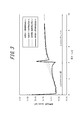
- the same evaluation was performed on the epitaxial wafers of Invention Example 3 and Comparative Example 3 that were not subjected to simulated heat treatment. The measurement results are shown in FIG. As is clear from FIG.
- the interface between the epitaxial layer and the silicon wafer in the epitaxial layer is greater after the simulated heat treatment than before the simulated heat treatment. It can be seen that the oxygen concentration increases in the nearby region.
- the dose amount of cluster ions is 2 ⁇ 10 14 atoms / cm 2
- the oxygen concentration profile before the simulated heat treatment and the oxygen concentration profile after the simulated heat treatment are substantially the same. It can be seen that the oxygen concentration rather decreases in the region near the interface with the wafer.
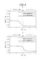
- FIG. 4 is a diagram for explaining how the resistivity variation in the silicon wafer is suppressed by the epitaxial wafer manufacturing method according to the present invention.
- 4A shows the resistivity distribution in the depth direction before and after the simulated heat treatment in the epitaxial wafer of Comparative Example 3
- FIG. 4B shows the before and after the simulated heat treatment in the epitaxial wafer of Invention Example 3.
- the resistivity distribution in the depth direction is shown.
- the resistivity distribution in the depth direction is measured by the SR method using a resistivity measuring device (model number: SSM2000, manufactured by Nippon SSM Co., Ltd.).
- Comparative Example 3 the resistivity decreases in the region near the interface between the epitaxial layer and the silicon wafer in the epitaxial layer after the simulated heat treatment. I understand that. In contrast, in Invention Example 3, it can be seen that the resistivity hardly fluctuates in the region near the interface between the epitaxial layer and the silicon wafer in the epitaxial layer.
- an epitaxial wafer having excellent gettering ability can be manufactured, which can suppress the diffusion of dopant and oxygen in a silicon wafer to the epitaxial layer during the heat treatment in the device formation process while suppressing the formation of epitaxial defects. This is useful in the semiconductor wafer manufacturing industry.
Landscapes
- Recrystallisation Techniques (AREA)
Abstract
Description
このように、現在、ウェーハに対してゲッタリング能力を付与するのが困難な状況にある。
そこで、本発明の目的は、エピタキシャル欠陥の形成を抑制しつつ、優れたゲッタリング能力を有するエピタキシャルウェーハを製造する方途を提供することにある。
しかし、一般的に、抵抗率の低いシリコンウェーハを用いて、シリコンウェーハよりも高い抵抗率のエピタキシャル層を形成したエピタキシャルウェーハは、デバイス形成工程における熱処理等により、シリコンウェーハ中のドーパントや酸素がエピタキシャル層内に拡散してエピタキシャル層の抵抗率が変動してしまう問題がある。
本発明者らの実験によれば、低抵抗率のシリコンウェーハに対して所定のドーズ量範囲でクラスターイオンを照射した場合には、エピタキシャル層内へのドーパントの拡散が抑制され、加えてシリコンウェーハ中の酸素もエピタキシャル層内に拡散することを抑制できることを知見し、本発明を完成させるに至った。
(1)0.001Ω・cm以上0.1Ω・cm以下の抵抗率を有するシリコンウェーハの表面に2.0×10¹⁴/cm2以上1.0×1016/cm2以下のドーズ量で少なくとも炭素を含むクラスターイオンを照射して、前記シリコンウェーハの表面部に、前記クラスターイオンの構成元素が固溶してなる改質層を形成するクラスターイオン照射工程と、前記シリコンウェーハの改質層上に前記シリコンウェーハよりも高い抵抗率を有するエピタキシャル層を形成するエピタキシャル層形成工程とを有することを特徴とするエピタキシャルウェーハの製造方法。
また、上記低抵抗率を有するシリコンウェーハへのクラスターイオンの照射を適正な範囲内にあるドーズ量で行うため、シリコンウェーハからエピタキシャル層への酸素およびドーパントの拡散を抑制し、エピタキシャル層の抵抗率の変動を抑制することができる。
以下、図面を参照して、本発明の実施形態について説明する。図1は、本発明によるエピタキシャルウェーハの製造方法を説明する模式断面図である。この図に示すエピタキシャルウェーハ100の製造方法は、シリコンウェーハ10の表面10Aに少なくとも炭素を含むクラスターイオン16を照射して、シリコンウェーハ10の表面部に、クラスターイオン16の構成元素が固溶してなる改質層18を形成するクラスターイオン照射工程と(図1(A)~(C))、シリコンウェーハ10の改質層18上にシリコンウェーハ10よりも高い抵抗率を有するエピタキシャル層20を形成するエピタキシャル層形成工程とを有する(図1(D))。ここで、シリコンウェーハ10として、0.001Ω・cm以上0.1Ω・cm以下の抵抗率を有するシリコンウェーハを用いること、およびクラスターイオン16の照射を2.0×10¹⁴atoms/cm2以上1.0×1016atoms/cm2以下のドーズ量で行うこと、が肝要である。
次に、本発明に係るエピタキシャルウェーハ100について説明する。図1(D)に示した、本発明に係るエピタキシャルウェーハ100は、0.001Ω・cm以上0.1Ω・cm以下の抵抗率を有するシリコンウェーハ10と、該シリコンウェーハ10の表面部に形成された、該シリコンウェーハ10中に少なくとも炭素を含む所定元素が固溶してなる改質層18と、該改質層18上に、シリコンウェーハ10よりも高い抵抗率を有するエピタキシャル層20とを有する。ここで、改質層18における所定元素の深さ方向の濃度プロファイルの半値幅が100nm以下であり、改質層18における濃度プロファイルのピーク濃度が、9.0×10¹⁸atoms/cm3以上1.0×1021atoms/cm3以下である。
以下、本発明の実施例について説明する。
まず、エピタキシャルウェーハの基板として、直径:300mm、厚さ:775μm、抵抗率:約0.003Ω・cmを有するシリコンウェーハを用意した。次いで、クラスターイオン発生装置(日新イオン機器社製、型番:CLARIS)を用いて、クラスターイオンとしてC3H5クラスターを生成し、炭素1原子当たりの加速電圧23.4keV/atomの条件でシリコンウェーハの表面に照射した。ここで、クラスターイオンのドーズ量は、1.0×1015atoms/cm2(発明例1)、5×1015atoms/cm2(発明例2)、2×1014atoms/cm2(発明例3)の3水準とした。続いて、シリコンウェーハを枚葉式エピタキシャル成長装置(アプライドマテリアルズ社製)内に搬送し、装置内で1120℃の温度で30秒の水素ベーク処理を施した。その後、水素をキャリアガス、トリクロロシランをソースガスとして、1150℃にてCVD法により、シリコンウェーハ上にシリコンのエピタキシャル層(厚さ:4.0μm、ドーパント:ホウ素、抵抗率:約0.3Ω・cm)をエピタキシャル成長させ、本発明に従うエピタキシャルウェーハとした。
比較例1として、基板として約10Ω・cmの抵抗率を有するシリコンウェーハを用いた以外は、発明例1と同様(すなわち、ドーズ量が1.0×10¹⁵atoms/cm2)にして、比較例1に係るエピタキシャルウェーハを作製した。
比較例2として、基板として約10Ω・cmの抵抗率を有するシリコンウェーハを用いた以外は、発明例2と同様(すなわち、ドーズ量が5×10¹⁵atoms/cm2)にして、比較例2に係るエピタキシャルウェーハを作製した。
比較例3として、シリコンウェーハに対してクラスターイオンを照射しなかった以外は、発明例1と同様にして、比較例3に係るエピタキシャルウェーハを作製した。
比較例4として、クラスターイオンのドーズ量を1×10¹⁴atoms/cm2の低ドーズ量に変更した以外は、発明例1と同様にして、比較例4に係るエピタキシャルウェーハを作製した。
上記発明例1~3および比較例1~4のエピタキシャルウェーハそれぞれについて、エピタキシャル層に形成されたエピタキシャル欠陥の数を評価した。具体的には、表面欠陥検査装置(KLA-Tencor社製:Surfscan SP-1)を用いて観察評価し、輝点欠陥(Light Point Defect, LPD)の発生状況を調べた。その際、観察モードはDCNモード(Dark Field Composite Normal mode)とし、具体的には、サイズ(直径)がDWNモード(Dark Field Wide Normal mode)で90nm以上かつDNNモード(Dark Field Narrow Normal mode)で110nm以上のLPDを検出する条件で行った。続いて、走査型電子顕微鏡(Scanning Electron Microscope, SEM)を用いて、LPDの発生部位を観察評価して、LPDが積層欠陥であるか否かを評価した。それぞれ10枚ずつ作製した発明例1~3および比較例1~4のウェーハに対してこの評価を実施し、ウェーハ1枚当たりの積層欠陥の平均の個数を求めた。その結果、ウェーハ1枚当たりの積層欠陥の平均の個数は、発明例1では3.2個、発明例2では2.8個(、発明例3では2.5個)であったのに対して、比較例1では5.0個、比較例2では6.0個(、比較例3では2.2個、比較例4では2.3個)であった。このように、ドーズ量を高めた発明例1および発明例2のエピタキシャルウェーハは、同じドーズ量である比較例1および比較例2のエピタキシャルウェーハよりもエピタキシャル欠陥の個数が低減され、低抵抗率を有する基板を用いることにより、エピタキシャル欠陥の形成を抑制できることが確認された。なお、クラスターイオンを照射しなかった比較例3、および1×10¹⁴atoms/cm2の低ドーズ量の比較例4のエピタキシャルウェーハは、エピタキシャル欠陥の個数が少なかった。
上記発明例1~3および比較例1~4のエピタキシャルウェーハそれぞれについてゲッタリング能力の評価を行った。具体的には、各エピタキシャルウェーハのエピタキシャル層表面をCu汚染液(1.0×10¹³/cm2)でスピンコート汚染法を用いて故意に汚染し、次いで1000℃、1時間の拡散熱処理を施した。その後、SIMS測定を行うことによりCuの濃度ピークを評価した。
その結果、発明例1~3(および比較例1、2)のエピタキシャルウェーハは全て1×10¹⁶atoms/cm2以上のCuのピーク濃度が検出されたのに対し、クラスターイオンを照射しなかった比較例3およびドーズ量が低い比較例4のエピタキシャルウェーハはCu濃度のピークが観察されなかった。クラスターイオンを照射する際のドーズ量を高めることによりゲッタリング能力が向上することが確認された。
次に、エピタキシャル層へのドーパントおよび酸素の拡散抑制効果とクラスターイオンのドーズ量との関係を調べるため、以下の実験を行った。
図3から明らかなように、クラスターイオンを照射しない(つまり、ドーズ量が0)比較例3では、模擬熱処理前に比べて模擬熱処理後では、エピタキシャル層におけるエピタキシャル層とシリコンウェーハとの間の界面近傍の領域において酸素濃度が増加していることが分かる。一方、クラスターイオンのドーズ量が2×10¹⁴atoms/cm2の発明例3では、模擬熱処理前の酸素濃度プロファイルと模擬熱処理後の酸素濃度プロファイルはほぼ同じであり、エピタキシャル層におけるエピタキシャル層とシリコンウェーハとの間の界面近傍の領域において酸素濃度はむしろ減少していることが分かる。
10A シリコンウェーハの表面
16 クラスターイオン
18 改質層
20 エピタキシャル層
100 エピタキシャルウェーハ
Claims (8)
- 0.001Ω・cm以上0.1Ω・cm以下の抵抗率を有するシリコンウェーハの表面に2.0×10¹⁴/cm2以上1.0×1016/cm2以下のドーズ量で少なくとも炭素を含むクラスターイオンを照射して、前記シリコンウェーハの表面部に、前記クラスターイオンの構成元素が固溶してなる改質層を形成するクラスターイオン照射工程と、
前記シリコンウェーハの改質層上に前記シリコンウェーハよりも高い抵抗率を有するエピタキシャル層を形成するエピタキシャル層形成工程と、
を有することを特徴とするエピタキシャルウェーハの製造方法。 - 前記クラスターイオンが構成元素として炭素を含む2種以上の元素を含む、請求項1に記載のエピタキシャルウェーハの製造方法。
- 前記シリコンウェーハの抵抗率は、ホウ素の添加により調整されたものである、請求項1または2に記載のエピタキシャルウェーハの製造方法。
- 前記クラスターイオン照射工程の後かつ前記エピタキシャル層形成工程の前に、非酸化性雰囲気において500℃以上1100℃以下の温度にて熱処理を行う熱処理工程をさらに有する、請求項1~3のいずれか一項に記載のエピタキシャルウェーハの製造方法。
- 0.001Ω・cm以上0.1Ω・cm以下の抵抗率を有するシリコンウェーハと、該シリコンウェーハの表面部に形成された、該シリコンウェーハ中に少なくとも炭素を含む所定元素が固溶してなる改質層と、該改質層上に、前記シリコンウェーハよりも高い抵抗率を有するエピタキシャル層と、を有し、
前記改質層における前記所定元素の深さ方向の濃度プロファイルの半値幅が100nm以下であり、前記改質層における前記濃度プロファイルのピーク濃度が、9.0×10¹⁸atoms/cm3以上1.0×1021atoms/cm3以下であることを特徴とするエピタキシャルウェーハ。 - 前記シリコンウェーハの表面からの深さが150nm以下の範囲内に、前記改質層における前記濃度プロファイルのピークが位置する、請求項5に記載のエピタキシャルウェーハ。
- 前記所定元素が炭素を含む2種以上の元素を含む、請求項5または6に記載のエピタキシャルウェーハ。
- 前記シリコンウェーハの抵抗率は、ホウ素の添加により調整されたものである、請求項5~7のいずれか一項に記載のエピタキシャルウェーハ。
Priority Applications (6)
| Application Number | Priority Date | Filing Date | Title |
|---|---|---|---|
| CN201480068022.XA CN106062937B (zh) | 2014-01-07 | 2014-12-10 | 外延晶片的制造方法和外延晶片 |
| DE112014006124.7T DE112014006124B4 (de) | 2014-01-07 | 2014-12-10 | Epitaxialwaferherstellungsverfahren und Epitaxialwafer |
| KR1020167016687A KR101856012B1 (ko) | 2014-01-07 | 2014-12-10 | 에피택셜 웨이퍼의 제조방법 및 에피택셜 웨이퍼 |
| US15/104,692 US10062569B2 (en) | 2014-01-07 | 2014-12-10 | Epitaxial wafer manufacturing method and epitaxial wafer |
| US15/996,924 US10453682B2 (en) | 2014-01-07 | 2018-06-04 | Epitaxial wafer manufacturing method and epitaxial wafer |
| US17/038,941 USRE49657E1 (en) | 2014-01-07 | 2020-09-30 | Epitaxial wafer manufacturing method and epitaxial wafer |
Applications Claiming Priority (2)
| Application Number | Priority Date | Filing Date | Title |
|---|---|---|---|
| JP2014-001074 | 2014-01-07 | ||
| JP2014001074A JP6056772B2 (ja) | 2014-01-07 | 2014-01-07 | エピタキシャルウェーハの製造方法およびエピタキシャルウェーハ |
Related Child Applications (2)
| Application Number | Title | Priority Date | Filing Date |
|---|---|---|---|
| US15/104,692 A-371-Of-International US10062569B2 (en) | 2014-01-07 | 2014-12-10 | Epitaxial wafer manufacturing method and epitaxial wafer |
| US15/996,924 Division US10453682B2 (en) | 2014-01-07 | 2018-06-04 | Epitaxial wafer manufacturing method and epitaxial wafer |
Publications (1)
| Publication Number | Publication Date |
|---|---|
| WO2015104755A1 true WO2015104755A1 (ja) | 2015-07-16 |
Family
ID=53523614
Family Applications (1)
| Application Number | Title | Priority Date | Filing Date |
|---|---|---|---|
| PCT/JP2014/006163 Ceased WO2015104755A1 (ja) | 2014-01-07 | 2014-12-10 | エピタキシャルウェーハの製造方法およびエピタキシャルウェーハ |
Country Status (7)
| Country | Link |
|---|---|
| US (3) | US10062569B2 (ja) |
| JP (1) | JP6056772B2 (ja) |
| KR (1) | KR101856012B1 (ja) |
| CN (1) | CN106062937B (ja) |
| DE (1) | DE112014006124B4 (ja) |
| TW (1) | TWI534306B (ja) |
| WO (1) | WO2015104755A1 (ja) |
Families Citing this family (9)
| Publication number | Priority date | Publication date | Assignee | Title |
|---|---|---|---|---|
| JP6504082B2 (ja) * | 2016-02-29 | 2019-04-24 | 株式会社Sumco | 半導体エピタキシャルウェーハおよびその製造方法ならびに固体撮像素子の製造方法 |
| JP2017201647A (ja) | 2016-05-02 | 2017-11-09 | ルネサスエレクトロニクス株式会社 | 半導体装置の製造方法 |
| DE102016125340A1 (de) * | 2016-12-22 | 2018-06-28 | Infineon Technologies Ag | Verfahren zum Bilden eines Halbleitersubstrats, Verfahren zum Bilden eines Halbleiterbauelements, Halbleitersubstrat und Halbleiterbauelement |
| JP6658613B2 (ja) * | 2017-02-27 | 2020-03-04 | 株式会社Sumco | エピタキシャルシリコンウェーハの不純物拡散挙動予測方法、ゲッタリング能力予測方法、ゲッタリング能力調整方法および製造方法 |
| JP6327393B1 (ja) * | 2017-02-28 | 2018-05-23 | 株式会社Sumco | エピタキシャルシリコンウェーハの不純物ゲッタリング能力の評価方法及びエピタキシャルシリコンウェーハ |
| JP6787268B2 (ja) * | 2017-07-20 | 2020-11-18 | 株式会社Sumco | 半導体エピタキシャルウェーハおよびその製造方法、ならびに固体撮像素子の製造方法 |
| CN109192743A (zh) * | 2018-09-04 | 2019-01-11 | 德淮半导体有限公司 | 图像传感器及其形成方法 |
| JP7035925B2 (ja) * | 2018-09-11 | 2022-03-15 | 株式会社Sumco | エピタキシャルシリコンウェーハの製造方法およびエピタキシャルシリコンウェーハ |
| JP6791293B2 (ja) * | 2019-04-03 | 2020-11-25 | 株式会社Sumco | エピタキシャルシリコンウェーハの製造方法 |
Citations (4)
| Publication number | Priority date | Publication date | Assignee | Title |
|---|---|---|---|---|
| JPH0817841A (ja) * | 1994-06-24 | 1996-01-19 | Fujitsu Ltd | 半導体基板,半導体装置及び半導体装置の製造方法 |
| WO2011125305A1 (ja) * | 2010-04-08 | 2011-10-13 | 信越半導体株式会社 | シリコンエピタキシャルウエーハ、シリコンエピタキシャルウエーハの製造方法、及び半導体素子又は集積回路の製造方法 |
| JP2012094575A (ja) * | 2010-10-25 | 2012-05-17 | Panasonic Corp | 半導体基板の製造方法 |
| WO2012157162A1 (ja) * | 2011-05-13 | 2012-11-22 | 株式会社Sumco | 半導体エピタキシャルウェーハの製造方法、半導体エピタキシャルウェーハ、および固体撮像素子の製造方法 |
Family Cites Families (11)
| Publication number | Priority date | Publication date | Assignee | Title |
|---|---|---|---|---|
| JPH05152304A (ja) | 1991-11-29 | 1993-06-18 | Sony Corp | 半導体基板の製造方法 |
| JP3384506B2 (ja) * | 1993-03-30 | 2003-03-10 | ソニー株式会社 | 半導体基板の製造方法 |
| CN1289722C (zh) | 2003-12-30 | 2006-12-13 | 宁波立立电子股份有限公司 | 用于重掺直拉硅单晶制造的掺杂方法及其掺杂漏斗 |
| US7259036B2 (en) * | 2004-02-14 | 2007-08-21 | Tel Epion Inc. | Methods of forming doped and un-doped strained semiconductor materials and semiconductor films by gas-cluster-ion-beam irradiation and materials and film products |
| KR100632463B1 (ko) * | 2005-02-07 | 2006-10-11 | 삼성전자주식회사 | 에피택셜 반도체 기판의 제조 방법과 이를 이용한 이미지센서의 제조 방법, 에피택셜 반도체 기판 및 이를 이용한이미지 센서 |
| JP2008294245A (ja) | 2007-05-25 | 2008-12-04 | Shin Etsu Handotai Co Ltd | エピタキシャルウェーハの製造方法およびエピタキシャルウェーハ |
| JP2009259959A (ja) * | 2008-04-15 | 2009-11-05 | Sumco Corp | 薄厚シリコンウェーハおよびその製造方法 |
| TWI504002B (zh) * | 2009-06-05 | 2015-10-11 | Semiconductor Energy Lab | 光電轉換裝置 |
| FR2962852A1 (fr) | 2010-07-19 | 2012-01-20 | Saint Gobain | Electrode transparente pour cellule photovoltaique a haut rendement |
| JP2012038973A (ja) | 2010-08-09 | 2012-02-23 | Siltronic Ag | シリコンウエハ及びその製造方法 |
| US10544517B2 (en) | 2011-05-06 | 2020-01-28 | Gtat Ip Holding Llc. | Growth of a uniformly doped silicon ingot by doping only the initial charge |
-
2014
- 2014-01-07 JP JP2014001074A patent/JP6056772B2/ja active Active
- 2014-12-10 DE DE112014006124.7T patent/DE112014006124B4/de active Active
- 2014-12-10 KR KR1020167016687A patent/KR101856012B1/ko active Active
- 2014-12-10 US US15/104,692 patent/US10062569B2/en active Active
- 2014-12-10 CN CN201480068022.XA patent/CN106062937B/zh active Active
- 2014-12-10 WO PCT/JP2014/006163 patent/WO2015104755A1/ja not_active Ceased
- 2014-12-31 TW TW103146424A patent/TWI534306B/zh active
-
2018
- 2018-06-04 US US15/996,924 patent/US10453682B2/en not_active Ceased
-
2020
- 2020-09-30 US US17/038,941 patent/USRE49657E1/en active Active
Patent Citations (4)
| Publication number | Priority date | Publication date | Assignee | Title |
|---|---|---|---|---|
| JPH0817841A (ja) * | 1994-06-24 | 1996-01-19 | Fujitsu Ltd | 半導体基板,半導体装置及び半導体装置の製造方法 |
| WO2011125305A1 (ja) * | 2010-04-08 | 2011-10-13 | 信越半導体株式会社 | シリコンエピタキシャルウエーハ、シリコンエピタキシャルウエーハの製造方法、及び半導体素子又は集積回路の製造方法 |
| JP2012094575A (ja) * | 2010-10-25 | 2012-05-17 | Panasonic Corp | 半導体基板の製造方法 |
| WO2012157162A1 (ja) * | 2011-05-13 | 2012-11-22 | 株式会社Sumco | 半導体エピタキシャルウェーハの製造方法、半導体エピタキシャルウェーハ、および固体撮像素子の製造方法 |
Also Published As
| Publication number | Publication date |
|---|---|
| KR20160089461A (ko) | 2016-07-27 |
| US10062569B2 (en) | 2018-08-28 |
| DE112014006124B4 (de) | 2023-06-22 |
| US10453682B2 (en) | 2019-10-22 |
| KR101856012B1 (ko) | 2018-05-09 |
| TWI534306B (zh) | 2016-05-21 |
| DE112014006124T5 (de) | 2016-09-22 |
| JP6056772B2 (ja) | 2017-01-11 |
| CN106062937A (zh) | 2016-10-26 |
| JP2015130396A (ja) | 2015-07-16 |
| CN106062937B (zh) | 2019-06-18 |
| USRE49657E1 (en) | 2023-09-12 |
| US20160351393A1 (en) | 2016-12-01 |
| TW201527609A (zh) | 2015-07-16 |
| US20180286677A1 (en) | 2018-10-04 |
Similar Documents
| Publication | Publication Date | Title |
|---|---|---|
| JP6056772B2 (ja) | エピタキシャルウェーハの製造方法およびエピタキシャルウェーハ | |
| JP5673811B2 (ja) | 半導体エピタキシャルウェーハの製造方法、半導体エピタキシャルウェーハ、および固体撮像素子の製造方法 | |
| JP6278591B2 (ja) | 半導体エピタキシャルウェーハの製造方法、半導体エピタキシャルウェーハ、および固体撮像素子の製造方法 | |
| CN107078029B (zh) | 半导体外延晶片和其制造方法以及固体摄像元件的制造方法 | |
| WO2015034075A1 (ja) | シリコンウェーハおよびその製造方法 | |
| WO2015104965A1 (ja) | 半導体エピタキシャルウェーハの製造方法、半導体エピタキシャルウェーハ、および固体撮像素子の製造方法 | |
| KR101856039B1 (ko) | 반도체 에피택셜 웨이퍼의 제조방법 및 고체 촬상 소자의 제조방법 | |
| JP6107068B2 (ja) | エピタキシャルシリコンウェーハの製造方法、エピタキシャルシリコンウェーハ、および固体撮像素子の製造方法 | |
| JP5938969B2 (ja) | エピタキシャルウエーハの製造方法および固体撮像素子の製造方法 | |
| TWI643250B (zh) | Method for manufacturing epitaxial wafer and epitaxial wafer | |
| JP6427894B2 (ja) | エピタキシャルウェーハの製造方法 | |
| JP6280301B2 (ja) | エピタキシャルシリコンウェーハの製造方法、エピタキシャルシリコンウェーハ、および固体撮像素子の製造方法 | |
| JP7416270B2 (ja) | エピタキシャルシリコンウェーハ及びその製造方法、並びに半導体デバイスの製造方法 | |
| JP6442817B2 (ja) | エピタキシャルウェーハの製造方法およびエピタキシャルウェーハ | |
| JP6278592B2 (ja) | 半導体エピタキシャルウェーハの製造方法、半導体エピタキシャルウェーハ、および固体撮像素子の製造方法 | |
| JP6361779B2 (ja) | エピタキシャルシリコンウェーハの製造方法、エピタキシャルシリコンウェーハ、および固体撮像素子の製造方法 | |
| JP2017123477A (ja) | 半導体エピタキシャルウェーハの製造方法、半導体エピタキシャルウェーハ、および固体撮像素子の製造方法 | |
| JP6318728B2 (ja) | 半導体エピタキシャルウェーハの製造方法、半導体エピタキシャルウェーハ、および固体撮像素子の製造方法 | |
| JP2015220242A (ja) | 半導体エピタキシャルウェーハの製造方法および固体撮像素子の製造方法 | |
| JP2017175143A (ja) | 半導体エピタキシャルウェーハの製造方法、半導体エピタキシャルウェーハ、および固体撮像素子の製造方法 |
Legal Events
| Date | Code | Title | Description |
|---|---|---|---|
| 121 | Ep: the epo has been informed by wipo that ep was designated in this application |
Ref document number: 14878317 Country of ref document: EP Kind code of ref document: A1 |
|
| WWE | Wipo information: entry into national phase |
Ref document number: 15104692 Country of ref document: US |
|
| ENP | Entry into the national phase |
Ref document number: 20167016687 Country of ref document: KR Kind code of ref document: A |
|
| WWE | Wipo information: entry into national phase |
Ref document number: 112014006124 Country of ref document: DE |
|
| 122 | Ep: pct application non-entry in european phase |
Ref document number: 14878317 Country of ref document: EP Kind code of ref document: A1 |