WO2015087997A1 - 半導体装置、並びにそれを用いたオルタネータ及び電力変換装置 - Google Patents
半導体装置、並びにそれを用いたオルタネータ及び電力変換装置 Download PDFInfo
- Publication number
- WO2015087997A1 WO2015087997A1 PCT/JP2014/082947 JP2014082947W WO2015087997A1 WO 2015087997 A1 WO2015087997 A1 WO 2015087997A1 JP 2014082947 W JP2014082947 W JP 2014082947W WO 2015087997 A1 WO2015087997 A1 WO 2015087997A1
- Authority
- WO
- WIPO (PCT)
- Prior art keywords
- electrode
- semiconductor device
- mosfet chip
- external electrode
- mosfet
- Prior art date
- Legal status (The legal status is an assumption and is not a legal conclusion. Google has not performed a legal analysis and makes no representation as to the accuracy of the status listed.)
- Ceased
Links
Images


Classifications
-
- H—ELECTRICITY
- H10—SEMICONDUCTOR DEVICES; ELECTRIC SOLID-STATE DEVICES NOT OTHERWISE PROVIDED FOR
- H10D—INORGANIC ELECTRIC SEMICONDUCTOR DEVICES
- H10D84/00—Integrated devices formed in or on semiconductor substrates that comprise only semiconducting layers, e.g. on Si wafers or on GaAs-on-Si wafers
- H10D84/101—Integrated devices comprising main components and built-in components, e.g. IGBT having built-in freewheel diode
- H10D84/141—VDMOS having built-in components
- H10D84/148—VDMOS having built-in components the built-in components being breakdown diodes, e.g. Zener diodes
-
- H—ELECTRICITY
- H02—GENERATION; CONVERSION OR DISTRIBUTION OF ELECTRIC POWER
- H02K—DYNAMO-ELECTRIC MACHINES
- H02K11/00—Structural association of dynamo-electric machines with electric components or with devices for shielding, monitoring or protection
-
- H—ELECTRICITY
- H02—GENERATION; CONVERSION OR DISTRIBUTION OF ELECTRIC POWER
- H02K—DYNAMO-ELECTRIC MACHINES
- H02K11/00—Structural association of dynamo-electric machines with electric components or with devices for shielding, monitoring or protection
- H02K11/04—Structural association of dynamo-electric machines with electric components or with devices for shielding, monitoring or protection for rectification
- H02K11/049—Rectifiers associated with stationary parts, e.g. stator cores
- H02K11/05—Rectifiers associated with casings, enclosures or brackets
-
- H—ELECTRICITY
- H02—GENERATION; CONVERSION OR DISTRIBUTION OF ELECTRIC POWER
- H02K—DYNAMO-ELECTRIC MACHINES
- H02K19/00—Synchronous motors or generators
- H02K19/16—Synchronous generators
- H02K19/36—Structural association of synchronous generators with auxiliary electric devices influencing the characteristic of the generator or controlling the generator, e.g. with impedances or switches
-
- H—ELECTRICITY
- H02—GENERATION; CONVERSION OR DISTRIBUTION OF ELECTRIC POWER
- H02M—APPARATUS FOR CONVERSION BETWEEN AC AND AC, BETWEEN AC AND DC, OR BETWEEN DC AND DC, AND FOR USE WITH MAINS OR SIMILAR POWER SUPPLY SYSTEMS; CONVERSION OF DC OR AC INPUT POWER INTO SURGE OUTPUT POWER; CONTROL OR REGULATION THEREOF
- H02M1/00—Details of apparatus for conversion
- H02M1/08—Circuits specially adapted for the generation of control voltages for semiconductor devices incorporated in static converters
-
- H—ELECTRICITY
- H02—GENERATION; CONVERSION OR DISTRIBUTION OF ELECTRIC POWER
- H02M—APPARATUS FOR CONVERSION BETWEEN AC AND AC, BETWEEN AC AND DC, OR BETWEEN DC AND DC, AND FOR USE WITH MAINS OR SIMILAR POWER SUPPLY SYSTEMS; CONVERSION OF DC OR AC INPUT POWER INTO SURGE OUTPUT POWER; CONTROL OR REGULATION THEREOF
- H02M7/00—Conversion of AC power input into DC power output; Conversion of DC power input into AC power output
- H02M7/003—Constructional details, e.g. physical layout, assembly, wiring or busbar connections
-
- H—ELECTRICITY
- H02—GENERATION; CONVERSION OR DISTRIBUTION OF ELECTRIC POWER
- H02M—APPARATUS FOR CONVERSION BETWEEN AC AND AC, BETWEEN AC AND DC, OR BETWEEN DC AND DC, AND FOR USE WITH MAINS OR SIMILAR POWER SUPPLY SYSTEMS; CONVERSION OF DC OR AC INPUT POWER INTO SURGE OUTPUT POWER; CONTROL OR REGULATION THEREOF
- H02M7/00—Conversion of AC power input into DC power output; Conversion of DC power input into AC power output
- H02M7/02—Conversion of AC power input into DC power output without possibility of reversal
- H02M7/04—Conversion of AC power input into DC power output without possibility of reversal by static converters
- H02M7/12—Conversion of AC power input into DC power output without possibility of reversal by static converters using discharge tubes with control electrode or semiconductor devices with control electrode
- H02M7/21—Conversion of AC power input into DC power output without possibility of reversal by static converters using discharge tubes with control electrode or semiconductor devices with control electrode using devices of a triode or transistor type requiring continuous application of a control signal
- H02M7/217—Conversion of AC power input into DC power output without possibility of reversal by static converters using discharge tubes with control electrode or semiconductor devices with control electrode using devices of a triode or transistor type requiring continuous application of a control signal using semiconductor devices only
- H02M7/219—Conversion of AC power input into DC power output without possibility of reversal by static converters using discharge tubes with control electrode or semiconductor devices with control electrode using devices of a triode or transistor type requiring continuous application of a control signal using semiconductor devices only in a bridge configuration
-
- H—ELECTRICITY
- H02—GENERATION; CONVERSION OR DISTRIBUTION OF ELECTRIC POWER
- H02P—CONTROL OR REGULATION OF ELECTRIC MOTORS, ELECTRIC GENERATORS OR DYNAMO-ELECTRIC CONVERTERS; CONTROLLING TRANSFORMERS, REACTORS OR CHOKE COILS
- H02P9/00—Arrangements for controlling electric generators for the purpose of obtaining a desired output
-
- H—ELECTRICITY
- H10—SEMICONDUCTOR DEVICES; ELECTRIC SOLID-STATE DEVICES NOT OTHERWISE PROVIDED FOR
- H10D—INORGANIC ELECTRIC SEMICONDUCTOR DEVICES
- H10D84/00—Integrated devices formed in or on semiconductor substrates that comprise only semiconducting layers, e.g. on Si wafers or on GaAs-on-Si wafers
- H10D84/101—Integrated devices comprising main components and built-in components, e.g. IGBT having built-in freewheel diode
- H10D84/141—VDMOS having built-in components
- H10D84/143—VDMOS having built-in components the built-in components being PN junction diodes
- H10D84/144—VDMOS having built-in components the built-in components being PN junction diodes in antiparallel diode configurations
-
- H—ELECTRICITY
- H10—SEMICONDUCTOR DEVICES; ELECTRIC SOLID-STATE DEVICES NOT OTHERWISE PROVIDED FOR
- H10W—GENERIC PACKAGES, INTERCONNECTIONS, CONNECTORS OR OTHER CONSTRUCTIONAL DETAILS OF DEVICES COVERED BY CLASS H10
- H10W40/00—Arrangements for thermal protection or thermal control
- H10W40/20—Arrangements for cooling
- H10W40/22—Arrangements for cooling characterised by their shape, e.g. having conical or cylindrical projections
-
- H—ELECTRICITY
- H10—SEMICONDUCTOR DEVICES; ELECTRIC SOLID-STATE DEVICES NOT OTHERWISE PROVIDED FOR
- H10W—GENERIC PACKAGES, INTERCONNECTIONS, CONNECTORS OR OTHER CONSTRUCTIONAL DETAILS OF DEVICES COVERED BY CLASS H10
- H10W40/00—Arrangements for thermal protection or thermal control
- H10W40/20—Arrangements for cooling
- H10W40/25—Arrangements for cooling characterised by their materials
-
- H—ELECTRICITY
- H10—SEMICONDUCTOR DEVICES; ELECTRIC SOLID-STATE DEVICES NOT OTHERWISE PROVIDED FOR
- H10W—GENERIC PACKAGES, INTERCONNECTIONS, CONNECTORS OR OTHER CONSTRUCTIONAL DETAILS OF DEVICES COVERED BY CLASS H10
- H10W46/00—Marks applied to devices, e.g. for alignment or identification
-
- H—ELECTRICITY
- H10—SEMICONDUCTOR DEVICES; ELECTRIC SOLID-STATE DEVICES NOT OTHERWISE PROVIDED FOR
- H10W—GENERIC PACKAGES, INTERCONNECTIONS, CONNECTORS OR OTHER CONSTRUCTIONAL DETAILS OF DEVICES COVERED BY CLASS H10
- H10W72/00—Interconnections or connectors in packages
-
- H—ELECTRICITY
- H10—SEMICONDUCTOR DEVICES; ELECTRIC SOLID-STATE DEVICES NOT OTHERWISE PROVIDED FOR
- H10W—GENERIC PACKAGES, INTERCONNECTIONS, CONNECTORS OR OTHER CONSTRUCTIONAL DETAILS OF DEVICES COVERED BY CLASS H10
- H10W74/00—Encapsulations, e.g. protective coatings
- H10W74/10—Encapsulations, e.g. protective coatings characterised by their shape or disposition
- H10W74/111—Encapsulations, e.g. protective coatings characterised by their shape or disposition the semiconductor body being completely enclosed
- H10W74/127—Encapsulations, e.g. protective coatings characterised by their shape or disposition the semiconductor body being completely enclosed characterised by arrangements for sealing or adhesion
-
- H—ELECTRICITY
- H10—SEMICONDUCTOR DEVICES; ELECTRIC SOLID-STATE DEVICES NOT OTHERWISE PROVIDED FOR
- H10W—GENERIC PACKAGES, INTERCONNECTIONS, CONNECTORS OR OTHER CONSTRUCTIONAL DETAILS OF DEVICES COVERED BY CLASS H10
- H10W74/00—Encapsulations, e.g. protective coatings
- H10W74/10—Encapsulations, e.g. protective coatings characterised by their shape or disposition
- H10W74/111—Encapsulations, e.g. protective coatings characterised by their shape or disposition the semiconductor body being completely enclosed
- H10W74/129—Encapsulations, e.g. protective coatings characterised by their shape or disposition the semiconductor body being completely enclosed forming a chip-scale package [CSP]
-
- H—ELECTRICITY
- H10—SEMICONDUCTOR DEVICES; ELECTRIC SOLID-STATE DEVICES NOT OTHERWISE PROVIDED FOR
- H10W—GENERIC PACKAGES, INTERCONNECTIONS, CONNECTORS OR OTHER CONSTRUCTIONAL DETAILS OF DEVICES COVERED BY CLASS H10
- H10W76/00—Containers; Fillings or auxiliary members therefor; Seals
- H10W76/10—Containers or parts thereof
- H10W76/12—Containers or parts thereof characterised by their shape
- H10W76/13—Containers comprising a conductive base serving as an interconnection
- H10W76/138—Containers comprising a conductive base serving as an interconnection having another interconnection being formed by a cover plate parallel to the conductive base, e.g. sandwich type
-
- H—ELECTRICITY
- H10—SEMICONDUCTOR DEVICES; ELECTRIC SOLID-STATE DEVICES NOT OTHERWISE PROVIDED FOR
- H10W—GENERIC PACKAGES, INTERCONNECTIONS, CONNECTORS OR OTHER CONSTRUCTIONAL DETAILS OF DEVICES COVERED BY CLASS H10
- H10W90/00—Package configurations
-
- H—ELECTRICITY
- H02—GENERATION; CONVERSION OR DISTRIBUTION OF ELECTRIC POWER
- H02M—APPARATUS FOR CONVERSION BETWEEN AC AND AC, BETWEEN AC AND DC, OR BETWEEN DC AND DC, AND FOR USE WITH MAINS OR SIMILAR POWER SUPPLY SYSTEMS; CONVERSION OF DC OR AC INPUT POWER INTO SURGE OUTPUT POWER; CONTROL OR REGULATION THEREOF
- H02M1/00—Details of apparatus for conversion
- H02M1/0003—Details of control, feedback or regulation circuits
- H02M1/0006—Arrangements for supplying an adequate voltage to the control circuit of converters
-
- H—ELECTRICITY
- H10—SEMICONDUCTOR DEVICES; ELECTRIC SOLID-STATE DEVICES NOT OTHERWISE PROVIDED FOR
- H10W—GENERIC PACKAGES, INTERCONNECTIONS, CONNECTORS OR OTHER CONSTRUCTIONAL DETAILS OF DEVICES COVERED BY CLASS H10
- H10W46/00—Marks applied to devices, e.g. for alignment or identification
- H10W46/101—Marks applied to devices, e.g. for alignment or identification characterised by the type of information, e.g. logos or symbols
-
- H—ELECTRICITY
- H10—SEMICONDUCTOR DEVICES; ELECTRIC SOLID-STATE DEVICES NOT OTHERWISE PROVIDED FOR
- H10W—GENERIC PACKAGES, INTERCONNECTIONS, CONNECTORS OR OTHER CONSTRUCTIONAL DETAILS OF DEVICES COVERED BY CLASS H10
- H10W46/00—Marks applied to devices, e.g. for alignment or identification
- H10W46/301—Marks applied to devices, e.g. for alignment or identification for alignment
-
- H—ELECTRICITY
- H10—SEMICONDUCTOR DEVICES; ELECTRIC SOLID-STATE DEVICES NOT OTHERWISE PROVIDED FOR
- H10W—GENERIC PACKAGES, INTERCONNECTIONS, CONNECTORS OR OTHER CONSTRUCTIONAL DETAILS OF DEVICES COVERED BY CLASS H10
- H10W46/00—Marks applied to devices, e.g. for alignment or identification
- H10W46/601—Marks applied to devices, e.g. for alignment or identification for use after dicing
- H10W46/607—Located on parts of packages, e.g. on encapsulations or on package substrates
-
- H—ELECTRICITY
- H10—SEMICONDUCTOR DEVICES; ELECTRIC SOLID-STATE DEVICES NOT OTHERWISE PROVIDED FOR
- H10W—GENERIC PACKAGES, INTERCONNECTIONS, CONNECTORS OR OTHER CONSTRUCTIONAL DETAILS OF DEVICES COVERED BY CLASS H10
- H10W72/00—Interconnections or connectors in packages
- H10W72/071—Connecting or disconnecting
- H10W72/0711—Apparatus therefor
- H10W72/07173—Means for moving chips, wafers or other parts, e.g. conveyor belts
-
- H—ELECTRICITY
- H10—SEMICONDUCTOR DEVICES; ELECTRIC SOLID-STATE DEVICES NOT OTHERWISE PROVIDED FOR
- H10W—GENERIC PACKAGES, INTERCONNECTIONS, CONNECTORS OR OTHER CONSTRUCTIONAL DETAILS OF DEVICES COVERED BY CLASS H10
- H10W72/00—Interconnections or connectors in packages
- H10W72/071—Connecting or disconnecting
- H10W72/0711—Apparatus therefor
- H10W72/07178—Means for aligning
-
- H—ELECTRICITY
- H10—SEMICONDUCTOR DEVICES; ELECTRIC SOLID-STATE DEVICES NOT OTHERWISE PROVIDED FOR
- H10W—GENERIC PACKAGES, INTERCONNECTIONS, CONNECTORS OR OTHER CONSTRUCTIONAL DETAILS OF DEVICES COVERED BY CLASS H10
- H10W72/00—Interconnections or connectors in packages
- H10W72/071—Connecting or disconnecting
- H10W72/073—Connecting or disconnecting of die-attach connectors
- H10W72/07331—Connecting techniques
- H10W72/07336—Soldering or alloying
-
- H—ELECTRICITY
- H10—SEMICONDUCTOR DEVICES; ELECTRIC SOLID-STATE DEVICES NOT OTHERWISE PROVIDED FOR
- H10W—GENERIC PACKAGES, INTERCONNECTIONS, CONNECTORS OR OTHER CONSTRUCTIONAL DETAILS OF DEVICES COVERED BY CLASS H10
- H10W72/00—Interconnections or connectors in packages
- H10W72/071—Connecting or disconnecting
- H10W72/073—Connecting or disconnecting of die-attach connectors
- H10W72/07351—Connecting or disconnecting of die-attach connectors characterised by changes in properties of the die-attach connectors during connecting
- H10W72/07354—Connecting or disconnecting of die-attach connectors characterised by changes in properties of the die-attach connectors during connecting changes in dispositions
-
- H—ELECTRICITY
- H10—SEMICONDUCTOR DEVICES; ELECTRIC SOLID-STATE DEVICES NOT OTHERWISE PROVIDED FOR
- H10W—GENERIC PACKAGES, INTERCONNECTIONS, CONNECTORS OR OTHER CONSTRUCTIONAL DETAILS OF DEVICES COVERED BY CLASS H10
- H10W72/00—Interconnections or connectors in packages
- H10W72/071—Connecting or disconnecting
- H10W72/075—Connecting or disconnecting of bond wires
-
- H—ELECTRICITY
- H10—SEMICONDUCTOR DEVICES; ELECTRIC SOLID-STATE DEVICES NOT OTHERWISE PROVIDED FOR
- H10W—GENERIC PACKAGES, INTERCONNECTIONS, CONNECTORS OR OTHER CONSTRUCTIONAL DETAILS OF DEVICES COVERED BY CLASS H10
- H10W72/00—Interconnections or connectors in packages
- H10W72/071—Connecting or disconnecting
- H10W72/076—Connecting or disconnecting of strap connectors
- H10W72/07631—Techniques
- H10W72/07636—Soldering or alloying
-
- H—ELECTRICITY
- H10—SEMICONDUCTOR DEVICES; ELECTRIC SOLID-STATE DEVICES NOT OTHERWISE PROVIDED FOR
- H10W—GENERIC PACKAGES, INTERCONNECTIONS, CONNECTORS OR OTHER CONSTRUCTIONAL DETAILS OF DEVICES COVERED BY CLASS H10
- H10W72/00—Interconnections or connectors in packages
- H10W72/30—Die-attach connectors
- H10W72/341—Dispositions of die-attach connectors, e.g. layouts
- H10W72/347—Dispositions of multiple die-attach connectors
-
- H—ELECTRICITY
- H10—SEMICONDUCTOR DEVICES; ELECTRIC SOLID-STATE DEVICES NOT OTHERWISE PROVIDED FOR
- H10W—GENERIC PACKAGES, INTERCONNECTIONS, CONNECTORS OR OTHER CONSTRUCTIONAL DETAILS OF DEVICES COVERED BY CLASS H10
- H10W72/00—Interconnections or connectors in packages
- H10W72/30—Die-attach connectors
- H10W72/351—Materials of die-attach connectors
- H10W72/352—Materials of die-attach connectors comprising metals or metalloids, e.g. solders
-
- H—ELECTRICITY
- H10—SEMICONDUCTOR DEVICES; ELECTRIC SOLID-STATE DEVICES NOT OTHERWISE PROVIDED FOR
- H10W—GENERIC PACKAGES, INTERCONNECTIONS, CONNECTORS OR OTHER CONSTRUCTIONAL DETAILS OF DEVICES COVERED BY CLASS H10
- H10W72/00—Interconnections or connectors in packages
- H10W72/30—Die-attach connectors
- H10W72/381—Auxiliary members
-
- H—ELECTRICITY
- H10—SEMICONDUCTOR DEVICES; ELECTRIC SOLID-STATE DEVICES NOT OTHERWISE PROVIDED FOR
- H10W—GENERIC PACKAGES, INTERCONNECTIONS, CONNECTORS OR OTHER CONSTRUCTIONAL DETAILS OF DEVICES COVERED BY CLASS H10
- H10W72/00—Interconnections or connectors in packages
- H10W72/50—Bond wires
- H10W72/541—Dispositions of bond wires
- H10W72/5434—Dispositions of bond wires the connected ends being on auxiliary connecting means on bond pads, e.g. on other bond wires
-
- H—ELECTRICITY
- H10—SEMICONDUCTOR DEVICES; ELECTRIC SOLID-STATE DEVICES NOT OTHERWISE PROVIDED FOR
- H10W—GENERIC PACKAGES, INTERCONNECTIONS, CONNECTORS OR OTHER CONSTRUCTIONAL DETAILS OF DEVICES COVERED BY CLASS H10
- H10W72/00—Interconnections or connectors in packages
- H10W72/50—Bond wires
- H10W72/541—Dispositions of bond wires
- H10W72/5445—Dispositions of bond wires being orthogonal to a side surface of the chip, e.g. parallel arrangements
-
- H—ELECTRICITY
- H10—SEMICONDUCTOR DEVICES; ELECTRIC SOLID-STATE DEVICES NOT OTHERWISE PROVIDED FOR
- H10W—GENERIC PACKAGES, INTERCONNECTIONS, CONNECTORS OR OTHER CONSTRUCTIONAL DETAILS OF DEVICES COVERED BY CLASS H10
- H10W72/00—Interconnections or connectors in packages
- H10W72/50—Bond wires
- H10W72/551—Materials of bond wires
- H10W72/552—Materials of bond wires comprising metals or metalloids, e.g. silver
- H10W72/5525—Materials of bond wires comprising metals or metalloids, e.g. silver comprising copper [Cu]
-
- H—ELECTRICITY
- H10—SEMICONDUCTOR DEVICES; ELECTRIC SOLID-STATE DEVICES NOT OTHERWISE PROVIDED FOR
- H10W—GENERIC PACKAGES, INTERCONNECTIONS, CONNECTORS OR OTHER CONSTRUCTIONAL DETAILS OF DEVICES COVERED BY CLASS H10
- H10W72/00—Interconnections or connectors in packages
- H10W72/50—Bond wires
- H10W72/59—Bond pads specially adapted therefor
-
- H—ELECTRICITY
- H10—SEMICONDUCTOR DEVICES; ELECTRIC SOLID-STATE DEVICES NOT OTHERWISE PROVIDED FOR
- H10W—GENERIC PACKAGES, INTERCONNECTIONS, CONNECTORS OR OTHER CONSTRUCTIONAL DETAILS OF DEVICES COVERED BY CLASS H10
- H10W72/00—Interconnections or connectors in packages
- H10W72/60—Strap connectors, e.g. thick copper clips for grounding of power devices
- H10W72/631—Shapes of strap connectors
- H10W72/634—Cross-sectional shape
-
- H—ELECTRICITY
- H10—SEMICONDUCTOR DEVICES; ELECTRIC SOLID-STATE DEVICES NOT OTHERWISE PROVIDED FOR
- H10W—GENERIC PACKAGES, INTERCONNECTIONS, CONNECTORS OR OTHER CONSTRUCTIONAL DETAILS OF DEVICES COVERED BY CLASS H10
- H10W72/00—Interconnections or connectors in packages
- H10W72/60—Strap connectors, e.g. thick copper clips for grounding of power devices
- H10W72/641—Dispositions of strap connectors
- H10W72/646—Dispositions of strap connectors the connected ends being on auxiliary connecting means on bond pads, e.g. on a bump connector
-
- H—ELECTRICITY
- H10—SEMICONDUCTOR DEVICES; ELECTRIC SOLID-STATE DEVICES NOT OTHERWISE PROVIDED FOR
- H10W—GENERIC PACKAGES, INTERCONNECTIONS, CONNECTORS OR OTHER CONSTRUCTIONAL DETAILS OF DEVICES COVERED BY CLASS H10
- H10W72/00—Interconnections or connectors in packages
- H10W72/60—Strap connectors, e.g. thick copper clips for grounding of power devices
- H10W72/651—Materials of strap connectors
- H10W72/652—Materials of strap connectors comprising metals or metalloids, e.g. silver
-
- H—ELECTRICITY
- H10—SEMICONDUCTOR DEVICES; ELECTRIC SOLID-STATE DEVICES NOT OTHERWISE PROVIDED FOR
- H10W—GENERIC PACKAGES, INTERCONNECTIONS, CONNECTORS OR OTHER CONSTRUCTIONAL DETAILS OF DEVICES COVERED BY CLASS H10
- H10W72/00—Interconnections or connectors in packages
- H10W72/851—Dispositions of multiple connectors or interconnections
- H10W72/853—On the same surface
- H10W72/871—Bond wires and strap connectors
-
- H—ELECTRICITY
- H10—SEMICONDUCTOR DEVICES; ELECTRIC SOLID-STATE DEVICES NOT OTHERWISE PROVIDED FOR
- H10W—GENERIC PACKAGES, INTERCONNECTIONS, CONNECTORS OR OTHER CONSTRUCTIONAL DETAILS OF DEVICES COVERED BY CLASS H10
- H10W72/00—Interconnections or connectors in packages
- H10W72/851—Dispositions of multiple connectors or interconnections
- H10W72/874—On different surfaces
- H10W72/884—Die-attach connectors and bond wires
-
- H—ELECTRICITY
- H10—SEMICONDUCTOR DEVICES; ELECTRIC SOLID-STATE DEVICES NOT OTHERWISE PROVIDED FOR
- H10W—GENERIC PACKAGES, INTERCONNECTIONS, CONNECTORS OR OTHER CONSTRUCTIONAL DETAILS OF DEVICES COVERED BY CLASS H10
- H10W72/00—Interconnections or connectors in packages
- H10W72/90—Bond pads, in general
- H10W72/921—Structures or relative sizes of bond pads
- H10W72/926—Multiple bond pads having different sizes
-
- H—ELECTRICITY
- H10—SEMICONDUCTOR DEVICES; ELECTRIC SOLID-STATE DEVICES NOT OTHERWISE PROVIDED FOR
- H10W—GENERIC PACKAGES, INTERCONNECTIONS, CONNECTORS OR OTHER CONSTRUCTIONAL DETAILS OF DEVICES COVERED BY CLASS H10
- H10W72/00—Interconnections or connectors in packages
- H10W72/90—Bond pads, in general
- H10W72/931—Shapes of bond pads
- H10W72/932—Plan-view shape, i.e. in top view
-
- H—ELECTRICITY
- H10—SEMICONDUCTOR DEVICES; ELECTRIC SOLID-STATE DEVICES NOT OTHERWISE PROVIDED FOR
- H10W—GENERIC PACKAGES, INTERCONNECTIONS, CONNECTORS OR OTHER CONSTRUCTIONAL DETAILS OF DEVICES COVERED BY CLASS H10
- H10W74/00—Encapsulations, e.g. protective coatings
-
- H—ELECTRICITY
- H10—SEMICONDUCTOR DEVICES; ELECTRIC SOLID-STATE DEVICES NOT OTHERWISE PROVIDED FOR
- H10W—GENERIC PACKAGES, INTERCONNECTIONS, CONNECTORS OR OTHER CONSTRUCTIONAL DETAILS OF DEVICES COVERED BY CLASS H10
- H10W74/00—Encapsulations, e.g. protective coatings
- H10W74/10—Encapsulations, e.g. protective coatings characterised by their shape or disposition
- H10W74/111—Encapsulations, e.g. protective coatings characterised by their shape or disposition the semiconductor body being completely enclosed
- H10W74/121—Encapsulations, e.g. protective coatings characterised by their shape or disposition the semiconductor body being completely enclosed by multiple encapsulations, e.g. by a thin protective coating and a thick encapsulation
-
- H—ELECTRICITY
- H10—SEMICONDUCTOR DEVICES; ELECTRIC SOLID-STATE DEVICES NOT OTHERWISE PROVIDED FOR
- H10W—GENERIC PACKAGES, INTERCONNECTIONS, CONNECTORS OR OTHER CONSTRUCTIONAL DETAILS OF DEVICES COVERED BY CLASS H10
- H10W90/00—Package configurations
- H10W90/701—Package configurations characterised by the relative positions of pads or connectors relative to package parts
- H10W90/731—Package configurations characterised by the relative positions of pads or connectors relative to package parts of die-attach connectors
- H10W90/736—Package configurations characterised by the relative positions of pads or connectors relative to package parts of die-attach connectors between a chip and a stacked lead frame, conducting package substrate or heat sink
-
- H—ELECTRICITY
- H10—SEMICONDUCTOR DEVICES; ELECTRIC SOLID-STATE DEVICES NOT OTHERWISE PROVIDED FOR
- H10W—GENERIC PACKAGES, INTERCONNECTIONS, CONNECTORS OR OTHER CONSTRUCTIONAL DETAILS OF DEVICES COVERED BY CLASS H10
- H10W90/00—Package configurations
- H10W90/701—Package configurations characterised by the relative positions of pads or connectors relative to package parts
- H10W90/751—Package configurations characterised by the relative positions of pads or connectors relative to package parts of bond wires
- H10W90/753—Package configurations characterised by the relative positions of pads or connectors relative to package parts of bond wires between laterally-adjacent chips
-
- H—ELECTRICITY
- H10—SEMICONDUCTOR DEVICES; ELECTRIC SOLID-STATE DEVICES NOT OTHERWISE PROVIDED FOR
- H10W—GENERIC PACKAGES, INTERCONNECTIONS, CONNECTORS OR OTHER CONSTRUCTIONAL DETAILS OF DEVICES COVERED BY CLASS H10
- H10W90/00—Package configurations
- H10W90/701—Package configurations characterised by the relative positions of pads or connectors relative to package parts
- H10W90/761—Package configurations characterised by the relative positions of pads or connectors relative to package parts of strap connectors
- H10W90/763—Package configurations characterised by the relative positions of pads or connectors relative to package parts of strap connectors between laterally-adjacent chips
Definitions
- the rectifying element using the diode has a problem that the loss is large because the diode has a built-in potential.
- a rectifying element using synchronous rectification of a MOSFET Metal Oxide Semiconductor Field Effect Transistor
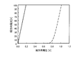
- the MOSFET has no built-in potential and has a low loss because a forward current rises from 0V. That is, since the MOSFET does not apply a voltage to pass the same current, the loss is reduced.
- FIG. 24 is a diagram showing forward current / voltage characteristics of a rectifying device using the MOSFET of the present invention and a rectifying device using a conventional diode.
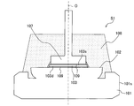
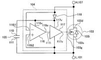
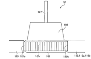
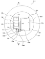
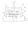
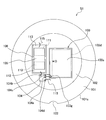
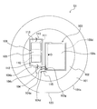
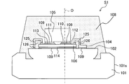
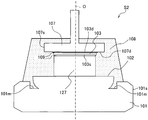
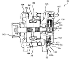
- the rectifying element S1 includes a base electrode 101 having a circular outer peripheral portion 101s in a top view, a pedestal 102 provided above the base electrode 101, a MOSFET chip 103 mounted on the pedestal 102, and a control.
- the circuit chip 104, the capacitor 105, and the lead electrode 107 (see FIG. 2) mounted on the MOSFET chip 103 are provided.
- the comparator 116 compares the voltage relationship between the H terminal (lead electrode 107) and the L terminal (base electrode 101), and the gate driver 117 turns the MOSFET chip 103 on / off.
- the capacitor 105 supplies a power supply voltage to the comparator 116 and the gate driver 117 via the power supply terminals 116v and 117v, respectively, using the stored charge.
- the circuit shown in FIG. 4 is an example of a control circuit that realizes the rectifying element S1 of the present invention, and is not limited to this.
- a differential amplifier that detects and amplifies a difference between input signals may be used, or on / off may be controlled by the direction of the current flowing through the MOSFET chip 103. Further, power may be supplied from the outside instead of the capacitor 105 shown in FIG.
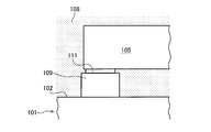
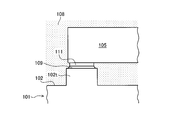
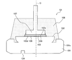
- the insulating substrate 106 is disposed only under the high-voltage side terminal 110 of the capacitor 105, A metal plate 120 or the like may be disposed under the side terminal 111 to electrically connect the base electrode 101 and the low voltage side terminal 111 of the capacitor 105. By doing so, the area required for connection between the base electrode 101 and the low voltage side terminal 111 of the capacitor 105 can be reduced.
- the adhesion between the MOSFET chip 103 and the control circuit chip 104 and the resin 108 is enhanced, and the occurrence of defects such as solder cracks and chip cracks occurring during the thermal fatigue test or the temperature cycle test is suppressed, and the rectifying element S1 Can improve the reliability.
- the groove 101m and / or JCR may be applied to the rectifying element S1 of the embodiment and rectifying elements S12 and S2 described later.
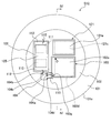
- a Zener diode chip 121 is disposed on the pedestal 102 at a position adjacent to the MOSFET chip 103.
- the cathode electrode 121c on the lower surface of the Zener diode chip 121 is used as the base electrode 101
- the anode electrode 121a on the upper surface of the Zener diode chip 121 is used as the lead electrode 107 as shown in FIG. 109 is electrically connected.
- a pin with spring 146A and a pin with spring 146B are fixed by a copper bar 147a.
- the pin 146A with a spring has a terminal 146a1 at the lower part, a spring 146b1 at the center, and a fixing part 146c1 at the upper part.
- the spring-loaded pin 146B has a terminal 146a2 at the lower part, a spring 146b2 at the center, and a fixing part 146c2 at the upper part.
- the circuit configuration and circuit operation of the rectifying element S2 of the synchronous rectification MOSFET according to the second embodiment are the same as the circuit configuration and circuit operation of the rectifying element S2 of the synchronous rectification MOSFET according to the first embodiment described with reference to FIG. is there.
- the design cost and the development cost can be reduced, and the same test is performed. Test costs can also be reduced.
- the cost can be reduced by mass production of the same parts and the same circuit.
Landscapes
- Engineering & Computer Science (AREA)
- Power Engineering (AREA)
- Rectifiers (AREA)
- Microelectronics & Electronic Packaging (AREA)
- Power Conversion In General (AREA)
- Metal-Oxide And Bipolar Metal-Oxide Semiconductor Integrated Circuits (AREA)
Priority Applications (3)
| Application Number | Priority Date | Filing Date | Title |
|---|---|---|---|
| US15/102,771 US10319849B2 (en) | 2013-12-12 | 2014-12-12 | Semiconductor device, and alternator and power conversion device which use same |
| EP14870416.6A EP3082243A4 (en) | 2013-12-12 | 2014-12-12 | Semiconductor device, and alternator and power conversion device which use same |
| CN201480067332.XA CN105814785B (zh) | 2013-12-12 | 2014-12-12 | 半导体装置、以及使用该半导体装置的交流发电机和电力变换装置 |
Applications Claiming Priority (2)
| Application Number | Priority Date | Filing Date | Title |
|---|---|---|---|
| JP2013-256619 | 2013-12-12 | ||
| JP2013256619A JP6263014B2 (ja) | 2013-12-12 | 2013-12-12 | 半導体装置、並びにそれを用いたオルタネータ及び電力変換装置 |
Publications (1)
| Publication Number | Publication Date |
|---|---|
| WO2015087997A1 true WO2015087997A1 (ja) | 2015-06-18 |
Family
ID=53371294
Family Applications (1)
| Application Number | Title | Priority Date | Filing Date |
|---|---|---|---|
| PCT/JP2014/082947 Ceased WO2015087997A1 (ja) | 2013-12-12 | 2014-12-12 | 半導体装置、並びにそれを用いたオルタネータ及び電力変換装置 |
Country Status (6)
| Country | Link |
|---|---|
| US (1) | US10319849B2 (https=) |
| EP (1) | EP3082243A4 (https=) |
| JP (1) | JP6263014B2 (https=) |
| CN (1) | CN105814785B (https=) |
| TW (1) | TWI530080B (https=) |
| WO (1) | WO2015087997A1 (https=) |
Cited By (2)
| Publication number | Priority date | Publication date | Assignee | Title |
|---|---|---|---|---|
| CN106711137A (zh) * | 2015-11-18 | 2017-05-24 | 株式会社日立功率半导体 | 半导体装置及采用该半导体装置的交流发电机 |
| JP2019122211A (ja) * | 2018-01-11 | 2019-07-22 | 株式会社デンソー | 回転電機 |
Families Citing this family (21)
| Publication number | Priority date | Publication date | Assignee | Title |
|---|---|---|---|---|
| DE102014115909B4 (de) * | 2014-10-31 | 2017-06-01 | Infineon Technologies Ag | Press-Pack-Zelle und Verfahren zum Betrieb einer Press-Pack-Zelle |
| JP2017022798A (ja) * | 2015-07-07 | 2017-01-26 | ルネサスエレクトロニクス株式会社 | 電力変換装置および駆動装置 |
| JP6617002B2 (ja) * | 2015-10-20 | 2019-12-04 | 株式会社 日立パワーデバイス | 整流器、それを用いたオルタネータおよび電源 |
| JP6561331B2 (ja) * | 2016-03-30 | 2019-08-21 | パナソニックIpマネジメント株式会社 | 半導体装置 |
| JP6869140B2 (ja) * | 2017-08-07 | 2021-05-12 | 株式会社 日立パワーデバイス | 半導体装置及びそれを用いたオルタネータ |
| JP6988518B2 (ja) | 2018-01-26 | 2022-01-05 | 株式会社デンソー | 整流装置及び回転電機 |
| TWI710138B (zh) * | 2018-06-21 | 2020-11-11 | 朋程科技股份有限公司 | 用於整流器的功率元件 |
| TWI664701B (zh) | 2018-07-04 | 2019-07-01 | 朋程科技股份有限公司 | 功率元件封裝結構 |
| CN110718542B (zh) * | 2018-07-11 | 2021-05-04 | 朋程科技股份有限公司 | 功率元件封装结构 |
| US11508808B2 (en) * | 2018-10-11 | 2022-11-22 | Actron Technology Corporation | Rectifier device, rectifier, generator device, and powertrain for vehicle |
| JP7231407B2 (ja) * | 2018-12-27 | 2023-03-01 | 株式会社 日立パワーデバイス | 半導体装置およびそれを用いたオルタネータ |
| US11587853B2 (en) * | 2019-09-03 | 2023-02-21 | Mediatek Inc. | Semiconductor devices having a serial power system |
| JP7232743B2 (ja) | 2019-10-24 | 2023-03-03 | 株式会社 日立パワーデバイス | 半導体装置及びそれを用いた整流素子、オルタネータ |
| FR3116966B1 (fr) * | 2020-12-01 | 2024-11-29 | Commissariat Energie Atomique | Convertisseur de puissance |
| JP7529946B2 (ja) * | 2021-02-17 | 2024-08-07 | ミネベアパワーデバイス株式会社 | 整流回路、整流回路の制御方法 |
| US11881437B2 (en) | 2021-10-27 | 2024-01-23 | Infineon Technologies Ag | Embedded package with electrically isolating dielectric liner |
| JP7827973B2 (ja) * | 2022-03-24 | 2026-03-11 | ミネベアパワーデバイス株式会社 | 半導体装置 |
| JP2024010725A (ja) * | 2022-07-13 | 2024-01-25 | 株式会社 日立パワーデバイス | オルタネータ用半導体装置およびオルタネータ |
| TWI836903B (zh) * | 2023-02-16 | 2024-03-21 | 朋程科技股份有限公司 | 能量轉換模組與能量轉換裝置 |
| JP2024175486A (ja) | 2023-06-06 | 2024-12-18 | ミネベアパワーデバイス株式会社 | 半導体装置及びそれを用いた電力変換装置 |
| CN118336561B (zh) * | 2024-04-24 | 2024-09-20 | 浙江汇升智能电器有限公司 | 一种智能并网电力成套设备 |
Citations (5)
| Publication number | Priority date | Publication date | Assignee | Title |
|---|---|---|---|---|
| JPH10215552A (ja) | 1996-08-08 | 1998-08-11 | Denso Corp | 交流発電機の整流装置とその製造方法 |
| JP2002165429A (ja) * | 2000-11-21 | 2002-06-07 | Denso Corp | 車両用交流発電機 |
| JP2003033038A (ja) | 2001-07-13 | 2003-01-31 | Mitsubishi Electric Corp | 車両用発電機の整流装置 |
| JP2005513760A (ja) * | 2001-08-17 | 2005-05-12 | ヴァレオ エキプマン エレクトリク モトゥール | 電子モジュール及びその組み立て方法 |
| JP2011507468A (ja) | 2007-12-14 | 2011-03-03 | ローベルト ボツシユ ゲゼルシヤフト ミツト ベシユレンクテル ハフツング | 整流器回路 |
Family Cites Families (7)
| Publication number | Priority date | Publication date | Assignee | Title |
|---|---|---|---|---|
| JP2841940B2 (ja) | 1990-12-19 | 1998-12-24 | 富士電機株式会社 | 半導体素子 |
| JPH1064796A (ja) | 1996-08-23 | 1998-03-06 | Mitsubishi Electric Corp | 半導体装置及びその製造方法 |
| US6476480B1 (en) * | 2000-07-10 | 2002-11-05 | Delphi Technologies, Inc. | Press-fit IC power package and method therefor |
| WO2006070581A1 (ja) | 2004-12-28 | 2006-07-06 | Kokusan Denki Co., Ltd. | 半導体装置 |
| JP4858290B2 (ja) * | 2006-06-05 | 2012-01-18 | 株式会社デンソー | 負荷駆動装置 |
| JP5734624B2 (ja) | 2010-11-12 | 2015-06-17 | 新光電気工業株式会社 | 半導体パッケージの製造方法 |
| JP6263108B2 (ja) * | 2014-09-11 | 2018-01-17 | 株式会社日立製作所 | 半導体装置、並びにそれを用いたオルタネータ及び電力変換装置 |
-
2013
- 2013-12-12 JP JP2013256619A patent/JP6263014B2/ja active Active
-
2014
- 2014-12-04 TW TW103142184A patent/TWI530080B/zh active
- 2014-12-12 EP EP14870416.6A patent/EP3082243A4/en active Pending
- 2014-12-12 CN CN201480067332.XA patent/CN105814785B/zh active Active
- 2014-12-12 WO PCT/JP2014/082947 patent/WO2015087997A1/ja not_active Ceased
- 2014-12-12 US US15/102,771 patent/US10319849B2/en active Active
Patent Citations (5)
| Publication number | Priority date | Publication date | Assignee | Title |
|---|---|---|---|---|
| JPH10215552A (ja) | 1996-08-08 | 1998-08-11 | Denso Corp | 交流発電機の整流装置とその製造方法 |
| JP2002165429A (ja) * | 2000-11-21 | 2002-06-07 | Denso Corp | 車両用交流発電機 |
| JP2003033038A (ja) | 2001-07-13 | 2003-01-31 | Mitsubishi Electric Corp | 車両用発電機の整流装置 |
| JP2005513760A (ja) * | 2001-08-17 | 2005-05-12 | ヴァレオ エキプマン エレクトリク モトゥール | 電子モジュール及びその組み立て方法 |
| JP2011507468A (ja) | 2007-12-14 | 2011-03-03 | ローベルト ボツシユ ゲゼルシヤフト ミツト ベシユレンクテル ハフツング | 整流器回路 |
Non-Patent Citations (1)
| Title |
|---|
| See also references of EP3082243A4 |
Cited By (4)
| Publication number | Priority date | Publication date | Assignee | Title |
|---|---|---|---|---|
| CN106711137A (zh) * | 2015-11-18 | 2017-05-24 | 株式会社日立功率半导体 | 半导体装置及采用该半导体装置的交流发电机 |
| EP3171401A3 (en) * | 2015-11-18 | 2017-06-28 | Hitachi Power Semiconductor Device, Ltd. | Semiconductor device and alternator using same |
| US10304761B2 (en) | 2015-11-18 | 2019-05-28 | Hitachi Power Semiconductor Device, Ltd. | Semiconductor device and alternator using same |
| JP2019122211A (ja) * | 2018-01-11 | 2019-07-22 | 株式会社デンソー | 回転電機 |
Also Published As
| Publication number | Publication date |
|---|---|
| EP3082243A4 (en) | 2017-12-06 |
| CN105814785A (zh) | 2016-07-27 |
| US20160315184A1 (en) | 2016-10-27 |
| CN105814785B (zh) | 2019-10-11 |
| TW201531009A (zh) | 2015-08-01 |
| JP6263014B2 (ja) | 2018-01-17 |
| EP3082243A1 (en) | 2016-10-19 |
| JP2015116053A (ja) | 2015-06-22 |
| US10319849B2 (en) | 2019-06-11 |
| TWI530080B (zh) | 2016-04-11 |
Similar Documents
| Publication | Publication Date | Title |
|---|---|---|
| JP6263014B2 (ja) | 半導体装置、並びにそれを用いたオルタネータ及び電力変換装置 | |
| JP6263108B2 (ja) | 半導体装置、並びにそれを用いたオルタネータ及び電力変換装置 | |
| CN103222161B (zh) | 用于旋转电机的互连的电子功率模块的架构以及包括该类型的架构的旋转电机 | |
| US10304761B2 (en) | Semiconductor device and alternator using same | |
| US9450477B2 (en) | B+ mounted integrated active rectifier electronics | |
| CN103229397B (zh) | 用于互连旋转电机的电子功率模块的方法以及通过该方法形成的互连的功率模块的组件 | |
| US20140361648A1 (en) | Electric rotating machine | |
| KR100379907B1 (ko) | 차량용 교류발전기 | |
| US20090160044A1 (en) | Semiconductor module mounting structure | |
| US20260018491A1 (en) | Semiconductor module and vehicle | |
| JP5754646B2 (ja) | 車両用回転電機 | |
| JP6006628B2 (ja) | パワー半導体装置、整流装置および電源装置 | |
| JP5561623B2 (ja) | 端子台、半導体装置および車両用回転電機 | |
| US12446197B2 (en) | Voltage converter and method for manufacturing a voltage converter | |
| KR20170070762A (ko) | 알터네이터 정류기 어셈블리 | |
| JP2004208467A (ja) | 多相交流回転電機搭載インバータ | |
| KR20180060270A (ko) | 알터네이터 정류기 어셈블리 |
Legal Events
| Date | Code | Title | Description |
|---|---|---|---|
| 121 | Ep: the epo has been informed by wipo that ep was designated in this application |
Ref document number: 14870416 Country of ref document: EP Kind code of ref document: A1 |
|
| WWE | Wipo information: entry into national phase |
Ref document number: 15102771 Country of ref document: US |
|
| REEP | Request for entry into the european phase |
Ref document number: 2014870416 Country of ref document: EP |
|
| WWE | Wipo information: entry into national phase |
Ref document number: 2014870416 Country of ref document: EP |
|
| NENP | Non-entry into the national phase |
Ref country code: DE |