WO2015083548A1 - 走査電子顕微鏡システム及びそれを用いたパターン計測方法並びに走査電子顕微鏡 - Google Patents
走査電子顕微鏡システム及びそれを用いたパターン計測方法並びに走査電子顕微鏡 Download PDFInfo
- Publication number
- WO2015083548A1 WO2015083548A1 PCT/JP2014/080661 JP2014080661W WO2015083548A1 WO 2015083548 A1 WO2015083548 A1 WO 2015083548A1 JP 2014080661 W JP2014080661 W JP 2014080661W WO 2015083548 A1 WO2015083548 A1 WO 2015083548A1
- Authority
- WO
- WIPO (PCT)
- Prior art keywords
- electron beam
- backscattered
- electron
- hole
- pattern
- Prior art date
- Legal status (The legal status is an assumption and is not a legal conclusion. Google has not performed a legal analysis and makes no representation as to the accuracy of the status listed.)
- Ceased
Links
Images


Classifications
-
- H—ELECTRICITY
- H01—ELECTRIC ELEMENTS
- H01J—ELECTRIC DISCHARGE TUBES OR DISCHARGE LAMPS
- H01J37/00—Discharge tubes with provision for introducing objects or material to be exposed to the discharge, e.g. for the purpose of examination or processing thereof
- H01J37/26—Electron or ion microscopes; Electron or ion diffraction tubes
- H01J37/29—Reflection microscopes
-
- G—PHYSICS
- G01—MEASURING; TESTING
- G01B—MEASURING LENGTH, THICKNESS OR SIMILAR LINEAR DIMENSIONS; MEASURING ANGLES; MEASURING AREAS; MEASURING IRREGULARITIES OF SURFACES OR CONTOURS
- G01B15/00—Measuring arrangements characterised by the use of electromagnetic waves or particle radiation, e.g. by the use of microwaves, X-rays, gamma rays or electrons
- G01B15/04—Measuring arrangements characterised by the use of electromagnetic waves or particle radiation, e.g. by the use of microwaves, X-rays, gamma rays or electrons for measuring contours or curvatures
-
- H—ELECTRICITY
- H01—ELECTRIC ELEMENTS
- H01J—ELECTRIC DISCHARGE TUBES OR DISCHARGE LAMPS
- H01J37/00—Discharge tubes with provision for introducing objects or material to be exposed to the discharge, e.g. for the purpose of examination or processing thereof
- H01J37/02—Details
- H01J37/244—Detectors; Associated components or circuits therefor
-
- H—ELECTRICITY
- H01—ELECTRIC ELEMENTS
- H01J—ELECTRIC DISCHARGE TUBES OR DISCHARGE LAMPS
- H01J37/00—Discharge tubes with provision for introducing objects or material to be exposed to the discharge, e.g. for the purpose of examination or processing thereof
- H01J37/26—Electron or ion microscopes; Electron or ion diffraction tubes
- H01J37/28—Electron or ion microscopes; Electron or ion diffraction tubes with scanning beams
-
- G—PHYSICS
- G01—MEASURING; TESTING
- G01B—MEASURING LENGTH, THICKNESS OR SIMILAR LINEAR DIMENSIONS; MEASURING ANGLES; MEASURING AREAS; MEASURING IRREGULARITIES OF SURFACES OR CONTOURS
- G01B2210/00—Aspects not specifically covered by any group under G01B, e.g. of wheel alignment, caliper-like sensors
- G01B2210/56—Measuring geometric parameters of semiconductor structures, e.g. profile, critical dimensions or trench depth
-
- H—ELECTRICITY
- H01—ELECTRIC ELEMENTS
- H01J—ELECTRIC DISCHARGE TUBES OR DISCHARGE LAMPS
- H01J2237/00—Discharge tubes exposing object to beam, e.g. for analysis treatment, etching, imaging
- H01J2237/244—Detection characterized by the detecting means
- H01J2237/24475—Scattered electron detectors
-
- H—ELECTRICITY
- H01—ELECTRIC ELEMENTS
- H01J—ELECTRIC DISCHARGE TUBES OR DISCHARGE LAMPS
- H01J2237/00—Discharge tubes exposing object to beam, e.g. for analysis treatment, etching, imaging
- H01J2237/244—Detection characterized by the detecting means
- H01J2237/2448—Secondary particle detectors
-
- H—ELECTRICITY
- H01—ELECTRIC ELEMENTS
- H01J—ELECTRIC DISCHARGE TUBES OR DISCHARGE LAMPS
- H01J2237/00—Discharge tubes exposing object to beam, e.g. for analysis treatment, etching, imaging
- H01J2237/244—Detection characterized by the detecting means
- H01J2237/24495—Signal processing, e.g. mixing of two or more signals
-
- H—ELECTRICITY
- H01—ELECTRIC ELEMENTS
- H01J—ELECTRIC DISCHARGE TUBES OR DISCHARGE LAMPS
- H01J2237/00—Discharge tubes exposing object to beam, e.g. for analysis treatment, etching, imaging
- H01J2237/26—Electron or ion microscopes
- H01J2237/28—Scanning microscopes
- H01J2237/2803—Scanning microscopes characterised by the imaging method
- H01J2237/2806—Secondary charged particle
-
- H—ELECTRICITY
- H01—ELECTRIC ELEMENTS
- H01J—ELECTRIC DISCHARGE TUBES OR DISCHARGE LAMPS
- H01J2237/00—Discharge tubes exposing object to beam, e.g. for analysis treatment, etching, imaging
- H01J2237/26—Electron or ion microscopes
- H01J2237/28—Scanning microscopes
- H01J2237/2809—Scanning microscopes characterised by the imaging problems involved
- H01J2237/281—Bottom of trenches or holes
-
- H—ELECTRICITY
- H01—ELECTRIC ELEMENTS
- H01J—ELECTRIC DISCHARGE TUBES OR DISCHARGE LAMPS
- H01J2237/00—Discharge tubes exposing object to beam, e.g. for analysis treatment, etching, imaging
- H01J2237/26—Electron or ion microscopes
- H01J2237/28—Scanning microscopes
- H01J2237/2813—Scanning microscopes characterised by the application
- H01J2237/2814—Measurement of surface topography
- H01J2237/2815—Depth profile
-
- H—ELECTRICITY
- H10—SEMICONDUCTOR DEVICES; ELECTRIC SOLID-STATE DEVICES NOT OTHERWISE PROVIDED FOR
- H10P—GENERIC PROCESSES OR APPARATUS FOR THE MANUFACTURE OR TREATMENT OF DEVICES COVERED BY CLASS H10
- H10P74/00—Testing or measuring during manufacture or treatment of wafers, substrates or devices
- H10P74/20—Testing or measuring during manufacture or treatment of wafers, substrates or devices characterised by the properties tested or measured, e.g. structural or electrical properties
- H10P74/203—Structural properties, e.g. testing or measuring thicknesses, line widths, warpage, bond strengths or physical defects
Definitions
- the present invention relates to a method for measuring dimensions of a pattern formed on a semiconductor wafer, and more particularly, to a scanning electron microscope system for measuring dimensions of a hole pattern or a groove pattern having a high aspect ratio, a pattern measuring method using the same, and a scanning method. It relates to an electron microscope.
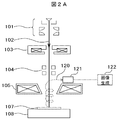
- FIG. 2A shows a basic configuration of a conventional length measuring SEM.
- the primary electron beam 102 emitted from the electron gun 101 is narrowed down by a condenser lens 103 and scanned on the sample two-dimensionally by a deflector 104.
- As the acceleration voltage a relatively low acceleration voltage of about 1 kV is generally used.
- a secondary electron beam image is obtained by capturing the secondary electrons 120 generated from the sample 107 by the electron beam irradiation with the detector 121. Since the pattern edge portion becomes a bright image on the secondary electron beam image due to the tilt angle effect or the edge effect, the dimension is obtained by detecting the edge position by an image processing method.
- a hole penetrating from the uppermost layer to the lowermost layer is formed at once (see FIG. 3A), a memory film is formed on the side surface of the hole, and a columnar electrode is embedded. It is formed through a process. The success or failure of this process is the drilling process, and the key is that a hole with an appropriate diameter penetrates to the lowest layer. There is a need to manage the opening / non-opening of holes or the top / bottom diameter of holes.
- Patent Document 1 discloses that electrons reflected from a side wall or a lower surface of a groove or hole of a sample penetrate through the sample.
- a scanning electron microscope that observes a hole pattern with an aspect ratio of about 3 by irradiating the sample with high-energy primary electrons that have sufficient energy to escape from the sample surface or generate tertiary electrons on the sample surface Are listed.
- the example of 100 kV and 200 kV is shown as the acceleration voltage of a primary electron.
- Patent Document 1 discloses a configuration in which reflected electrons are arranged between an objective lens and a spectroscope and detected by a scintillator, and tertiary electrons that have passed through the central cavity of the objective lens are extracted by an extraction electric field and detected by the scintillator. Is described.
- Patent Document 2 a sample is irradiated with an electron beam accelerated at 50 kV or higher using a scanning electron microscope, and secondary electrons and tertiary electrons generated from the sample are detected with a scintillator, and holes or grooves are detected. It is described that the inside is observed.
- reflected electrons are arranged between the objective lens and the sample and detected by the scintillator, and the tertiary electrons that have passed through the central cavity of the objective lens are extracted by the extraction electric field and detected by the scintillator. The configuration is described.
- the high-energy reflected electrons generated from the bottom of the hole and the tertiary electrons generated when the high-energy reflected electrons pass through the side wall of the hole are obtained by the suction electrode.
- separates and each detects is described.
- the level of the tertiary signal generated from a sample having a narrow and deep hole with a large aspect ratio is generally low. Therefore, in the configuration in which the tertiary electrons as described in Patent Document 1 are detected by sucking with the suction electrode, only a part of the tertiary electrons generated from the sample can be detected, and the aspect ratio is small. When observing a deep hole, it is difficult to ensure a sufficient detection signal level of tertiary electrons.
- the reflected electrons described in Patent Document 1 are detected by a scintillator arranged between the objective lens and the sample, and the tertiary electrons that have passed through the central cavity of the objective lens are extracted by an extraction electric field and detected by the scintillator.
- the tertiary electrons generated from the sample that have passed through the central cavity of the objective lens can be detected, and it is difficult to ensure a sufficient detection signal level of the tertiary electrons.
- the reflected electrons generated from the bottom of the deep hole having a large aspect ratio the reflected electrons emitted to the outside from the opening of the hole have more components that travel in the direction along the center axis of the hole.
- the disclosed scintillator can detect only a part of the tertiary electrons generated from the sample, and a sufficient detection signal of the tertiary electrons.
- the backscattered electrons generated from the bottom of a deep hole with a large aspect ratio have more components that travel in the direction along the center axis of the hole. It is difficult to detect with a scintillator arranged around the area except the part.
- the present invention solves the above-mentioned problems of the prior art, enables measurement of a hole diameter or groove width with a high aspect ratio, and enables measurement of a hole or groove depth and a scanning electron microscope system thereof And a scanning electron microscope.
- a scanning electron microscope system that measures a hole pattern or a groove pattern formed on a substrate is scanned with a primary electron beam with respect to the pattern formed on the substrate.
- Backscattering for detecting backscattered electrons penetrating through the side wall of the hole pattern or groove pattern among the irradiated primary electron beam irradiation means and the backscattered electrons emitted from the substrate irradiated with the primary electron beam by the primary electron beam irradiation means
- Electron detection means, electron beam image generation means for generating an electron beam image corresponding to the intensity distribution of backscattered electrons detected by the backscattered electron detection means, and a bright portion on the electron beam image generated by the electron beam image generation means
- Image processing means for obtaining a boundary area between the dark area and the bright area existing in the area and detecting the obtained boundary area as an edge position of a hole pattern or a groove pattern.
- a scanning electron microscope system that measures a hole pattern or a groove pattern formed on a substrate is scanned with a primary electron beam with respect to the pattern formed on the substrate. And detecting backscattered electrons penetrating through the side wall of the hole pattern or groove pattern among the backscattered electrons emitted from the substrate irradiated with the primary electron beam by the primary electron beam irradiating means.
- Backscattered electron detection means electron beam image generation means for generating an electron beam image corresponding to the intensity distribution of backscattered electrons detected by the backscattered electron detection means, and on the electron beam image generated by the electron beam image generation means
- the boundary area between the dark area and the bright area existing in the bright area is obtained, and the depth of the hole pattern or groove pattern is estimated from the brightness information of the dark area inside the obtained boundary area. It was constructed and a depth estimation means for.
- a scanning electron microscope system that measures a hole pattern or a groove pattern formed on a substrate is scanned with a primary electron beam with respect to the pattern formed on the substrate. And detecting backscattered electrons penetrating through the side wall of the hole pattern or groove pattern among the backscattered electrons emitted from the substrate irradiated with the primary electron beam by the primary electron beam irradiating means.
- Backscattered electron detection means electron beam image generation means for generating an electron beam image corresponding to the intensity distribution of backscattered electrons detected by the backscattered electron detection means, and on the electron beam image generated by the electron beam image generation means
- An image processing means for obtaining a boundary area with a bright area of a dark area existing in the bright area and detecting the obtained boundary area as an edge position of a hole pattern or a groove pattern; The boundary area between the bright area and the dark area existing in the bright area on the electron beam image generated by the sub-line image generation means is obtained, and the brightness information of the dark area inside the obtained boundary area is obtained.
- a depth estimating means for estimating the depth of the hole pattern or groove pattern.
- the pattern is formed on the substrate with an electron microscope.
- Back-scattered electrons penetrating through the sidewalls of the hole pattern or groove pattern among the back-scattered electrons emitted from the substrate irradiated with the primary electron beam are scanned and irradiated to the hole pattern or groove pattern.
- Detecting generating an electron beam image corresponding to the detected intensity distribution of the backscattered electrons, obtaining a boundary region between the bright region and the bright region in the bright region on the generated electron beam image,
- the detected boundary area is detected as the edge position of the hole pattern or groove pattern, and the information on the brightness of the dark area inside the boundary area is obtained. And to perform either or both to estimate is.
- an electron microscope that measures the hole pattern or groove pattern formed on the substrate is scanned with the primary electron beam with respect to the pattern formed on the substrate. And detecting backscattered electrons penetrating through the side wall of the hole pattern or groove pattern among the backscattered electrons emitted from the substrate irradiated with the primary electron beam by the primary electron beam irradiating means.
- the apparatus includes a scattered electron detection unit and an electron beam image generation unit that generates an electron beam image corresponding to the intensity distribution of the backscattered electrons detected by the backscattered electron detection unit.
- the present invention it is possible to measure a hole diameter with a high aspect ratio and to measure a hole depth.
- 1 is a block diagram showing a configuration of a scanning electron microscope system according to a first embodiment of the present invention.
- 1 is a plan view of a scintillator according to a first embodiment of the present invention. It is sectional drawing of the hole pattern which shows typically the state which the backscattered electron (BSE) generate
- BSE backscattered electron
- FIG. 6 is a signal waveform diagram showing a state in which a bottom diameter is calculated by applying Bottom line and Slope line to a signal waveform in a cross section AA of a low-angle BSE image of a hole pattern.
- FIG. In the 2nd example of the present invention it is a graph which shows intensity distribution of backscattered electrons (BSE) detected when a primary electron beam is irradiated to a hole pattern from which depth differs.
- BSE backscattered electrons
- FIG. 6 is a face view of a sample on which a hole pattern is schematically shown in a state in which backscattered electrons are generated from the hole bottom when the sample on which the hole pattern is formed is irradiated with a primary electron beam. It is the graph which calculated
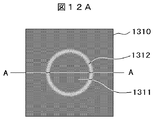
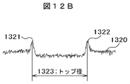
- FIG. 12B is a signal waveform diagram showing a signal waveform in the AA cross section of the secondary electron image of FIG. 12A. It is a perspective view of the hole pattern which shows the top diameter d1, the hole depth h, and the bottom diameter d2 of the hole pattern which concerns on a 3rd Example. It is a schematic diagram of SE image concerning the 3rd example of the present invention. It is a schematic diagram of the BSE image which concerns on the 3rd Example of this invention. It is a block diagram which shows the structure of the imaging optical system of the scanning electron microscope system which concerns on the 4th Example of this invention.
- the present invention irradiates a specimen with an electron beam having a high acceleration voltage and detects backscattered electrons (BSE) at a low angle (for example, an elevation angle of 5 degrees or more), thereby ejecting from a hole bottom and penetrating a side wall.
- BSE backscattered electrons
- the elevation angle is defined as the angle formed by the normal direction of the surface of the sample to be measured and the emission direction of the emitted electrons.
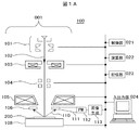
- FIG. 1A shows a basic configuration of a scanning electron microscope system 100 to which the present invention is applied.
- the electron microscope system 100 includes an imaging optical system 001, a control unit 021, a calculation unit 022, a storage unit 023, an input / output unit 024, and the like.
- the imaging optical system 001 generates a primary electron beam 102 having a high acceleration voltage (for example, 30 kV or more) from the electron gun 101, converges the primary electron beam 102 with a condenser lens 103, and passes it through the objective lens 105. Focus on the surface of the sample 200.
- a high acceleration voltage for example, 30 kV or more
- the primary electron beam 102 is scanned two-dimensionally on the sample 200 by the deflector 104.
- the low-angle backscattered electrons 110 emitted from the sample 200 are received by an annular YAG scintillator 106 (see FIG. 1B), converted into an optical signal, guided to a high electron multiplier 112 by an optical fiber 111, and an image generator.
- a digital image is generated at step 113.
- brightness correction is generally performed so that the image has an appropriate brightness.
- the captured image is stored in the storage unit 023. By moving the stage 108, it is possible to capture an image at an arbitrary position of the sample.
- the control unit 021 controls the voltage applied to the periphery of the electron gun 101, the focal position adjustment of the condenser lens 104 and the objective lens 105, the movement of the stage 108, the operation timing of the image generation unit 113, and the like.
- the arithmetic unit 022 performs dimension measurement processing using the captured image.
- the input / output unit 024 performs input of sample information, input of imaging conditions, output of dimension measurement results, and the like.
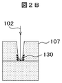
- BSE is emitted if primary electrons are irradiated to the bottom of the hole.
- the primary electrons are low energy (low acceleration voltage)
- the energy of BSE is also low. The energy is lost while proceeding, and cannot be penetrated (see FIG. 2B).
- a combination of a high acceleration voltage and a low angle BSE (a BSE generated in a direction in which the angle formed by the normal direction of the surface of the sample 200 is relatively large) is used to detect “punch-through BSE”, which is different from the conventional detection. It can be said that the hole bottom observation based on the principle was made possible.
- annular semiconductor detector For detecting low-angle BSE, an annular semiconductor detector or a Robinson detector may be used in addition to the YAG scintillator 106. Moreover, you may comprise so that a detector may be arrange
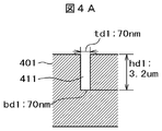
- the cross-sectional shape of the hole 411 formed in the sample 401 is a hole having a top diameter td1: 70 nm, a bottom diameter bd1: 70 nm, a hole depth hd1: 3.2 ⁇ m (hereinafter referred to as a t70b70 hole).
- a t70b70 hole a hole having a top diameter td1: 70 nm, a bottom diameter bd1: 70 nm, a hole depth hd1: 3.2 ⁇ m (hereinafter referred to as a t70b70 hole).
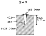
- the cross-sectional shape of the hole 412 formed in the sample 402 is a hole having a top diameter td2: 70 nm, a bottom diameter bd2: 30 nm, and a hole depth hd2: 3.2 ⁇ m (hereinafter referred to as a t70b30 hole). Indicates.
- the acceleration voltage is 30 kV
- a secondary electron image (Secondary Electron Image: SE image) detects electrons having an energy of 50 eV or less
- a low angle BSE image has an energy of 5000 eV or more and an elevation angle of emitted electrons (this specification)
- the elevation angle is defined as the angle formed between the normal direction of the surface of the sample 200 and the emission direction of the emitted electrons), which was obtained by detecting 15-65 degree electrons.
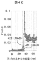
- the signal waveform of the SE image detected when the primary electron beam 102 is irradiated to the samples 401 and 402 in which the holes 411 and 412 having the different cross-sectional shapes shown in FIGS. 4A and 4B are formed is shown in FIG.
- the signal waveform of the image is shown in FIG. 4D.
- the vertical axis in the figure is the detection signal intensity (Yield).
- the signal waveform 422 of the low-angle BSE image detected from the sample 402 the signal intensity at the bottom of the hole is requisitely small, and it is difficult to detect the bottom edge position from this signal waveform.
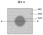
- FIGS. 5A to 5C A specific method for detecting the hole bottom edge position is shown in FIGS. 5A to 5C.
- the low-angle BSE image 501 of the hole pattern is an image in which the inside of the hole 502 is dark and the outside of the hole 503 is bright.
- the image has a sharp edge, and when the hole side wall has a taper, the image has a blurred edge.
- Signal waveforms 510 and 520 in FIGS. 5B and 5C are AA slice waveforms across hole 502 in FIG. 5A.
- FIG. 4D since the bottom edge end is the rising position of the signal waveform, as shown in FIG.
- Bottom line: 511 and Slope line: 512 are respectively applied to the bottom area and the slope area of the signal waveform. By fitting, these intersections are detected as bottom edge ends 513, and a bottom diameter 514 is obtained.
- a threshold value that internally divides the max value 521 and the min value 522 of the signal waveform by an appropriate ratio may be given, and the intersection of the threshold value and the signal waveform may be set as an edge point. At this time, two threshold values (th1: 523 and th2: 524) may be given to obtain the hole diameter 1: 525 and the hole diameter 2: 526.
- the size of the side wall taper can be monitored by the magnitude of the side wall inclination angle index value. It is.
- the first embodiment described above is the basic configuration of the present invention. According to the present embodiment, it is possible to measure a hole diameter with a high aspect ratio, which is impossible to measure with the prior art.
- the present embodiment provides a method for measuring not only the hole diameter but also the hole depth.
- the present invention realizes hole bottom observation by detecting BSE that penetrates the side wall, but when the hole is deep and the aspect ratio is large, electrons emitted from the bottom of the hole penetrate the side wall and reach the surface. Since the distance required for this becomes longer, the proportion of electrons that cannot be penetrated by using up energy on the way increases. In other words, it is possible to measure (estimate) the hole depth by using the relationship that the deeper the hole is, the darker the hole is on the captured image.
- the configuration of the scanning electron microscope system used in the present embodiment is the same as the configuration of the scanning electron microscope system 100 shown in FIG. 1A described in the first embodiment.
- FIG. 6A is a comparison of signal waveforms 611 and 612 of a low-angle BSE image detected when a primary electron beam is irradiated to a hole depth of 2.0 ⁇ m and a 3.2 ⁇ m hole formed in a sample, respectively.
- 6 is a graph 610 showing In any case, the top diameter (corresponding to td2 in FIG. 4B) of the hole pattern formed in the sample is 70 nm, the bottom diameter (corresponding to bd2 in FIG. 4B) is 30 nm, and the acceleration voltage and other conditions are as shown in FIG. This is the same as the simulation described in 4D.
- the hole depth of the hole pattern (corresponding to hd2 in FIG.
- the signal intensity of the signal 6111 in which the BSE is detected from the portion corresponding to the hole bottom in the signal waveform 611 is 3.2 ⁇ m. It can be seen that the signal intensity of the signal 6121 in which the BSE is detected from the portion corresponding to the hole bottom in the signal waveform 612 is clearly smaller. This is a feature that is significantly different from the conventional technique for detecting SE.
- FIG. 6B shows a signal in which BSE is detected from the portion corresponding to the hole depth and the bottom of the hole pattern formed in the sample when the acceleration voltage of the primary electrons irradiated to the sample is 15 kV, 30 kV, and 45 kV (signal 6111 and FIG. 6A).
- 6120 is a graph 620 showing the relationship between the signal strengths (yield) 621, 622, and 623 (corresponding to 6121). The signal intensity is higher when the acceleration voltage is higher because the number of electrons penetrating the side wall and reaching the uppermost surface of the sample is increased due to the higher energy of BSE.
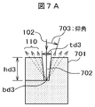
- FIG. 7A and FIG. 7B are the results of a simulation performed to clarify the range of the elevation angle (see FIG. 7A) suitable for detecting the punch-through BSE. Similar to the case described with reference to FIGS. 6A and 6B, the top diameter td3 of the hole pattern formed in the sample was 70 nm, and the bottom diameter bd3 was 30 nm.
- a graph 710 in FIG. 7B shows the distribution of signal intensity with respect to the elevation angle when the hole depth hd3 is 0.1 ⁇ m, 0.6 ⁇ m, and 1.2 ⁇ m.
- the range of the elevation angle 703 in which the emitted electrons are detected is 15 to 65 degrees.
- the entire elevation angle is detected.
- the elevation angle is 5 degrees or less, there is not much difference in signal intensity even if the hole depth is different. This is because many electrons radiated from the bottom of the hole and escaped from the hole opening immediately above the hole are included (the signal intensity changes depending on the depth of the hole depends on the difference in the passing distance in the side wall. Therefore, in the case of electrons not passing through the side wall, there is no difference in signal intensity due to the hole depth). It can be seen that it is desirable to detect a low-angle BSE with an elevation angle of 5 degrees or more for measuring the hole depth.
- the annular scintillator 106 provided between the sample 200 and the objective lens 105 is used for detecting BSE (see FIG. 1), the high-angle BSE passes through the hole 1061 in the center of the scintillator 106. . Therefore, the high angle (small elevation angle 703) BSE that has passed through the hole 1061 in the center of the scintillator 106 is not detected by the scintillator 106, so this requirement is satisfied.
- the cover range of the elevation angle for detecting the BSE by the scintillator 106 is wide. From the relationship between the elevation angle and the BSE signal intensity shown in the graph 710 of FIG. 7B, it is desirable to cover at least the range of the elevation angle of 20 to 60 degrees where the signal intensity of the BSE detection signal is large. In the present embodiment, this requirement can be satisfied by adjusting the diameter of the scintillator 106 and the distance between the scintillator 106 and the sample 200.
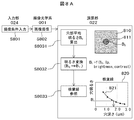
- FIG. 8A is a flowchart showing a process flow of hole depth measurement.
- Imaging conditions such as imaging magnification and acceleration voltage are input from the input unit 024 in the scanning electron microscope system 100 shown in FIG. 1A (S801).
- an image of the sample 200 is acquired based on the condition input in S801de by the imaging optical system 001 (S802).
- An image signal obtained by imaging the sample 200 with the imaging optical system 001 is input to the calculation unit 022 (S803).
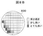
- the brightness of the hole is converted from B 0 to B 1 because the brightness of the hole on the image also changes depending on the beam current value and the brightness correction value. This is because there is no point in referring to the calibration curve without conversion. In other words, the calibration curve 821 needs to have a relationship between the hole depth and the hole brightness as shown in the wafer map 830 of FIG. 8B under the reference condition.
- a graph 910 in FIG. 9A shows the atomic number dependency 911 of the reflected electron intensity.
- Typical materials used in the semiconductor process are plotted on a graph. In parentheses are the average atomic numbers.
- SiO2 and Si are used for the laminated film material (201 and 202 in FIG. 3A), and SiGe is used for the stopper film (205 in FIG. 3A). Since the intensity of the punch-through BSE also changes in proportion to the reflected electron intensity, it is necessary to have a calibration curve as data for each acceleration voltage for each material. Further, as shown in FIG.
- the intensity of the penetration BSE varies depending on the acceleration voltage of the primary electron beam 102 irradiated to the sample 200. Therefore, as shown in the graph 920 in FIG. 9B and the graph 930 in FIG. 9C, it is necessary to have calibration curve data for each material and each acceleration voltage.
- the calibration curve data can be created by measuring the brightness of the hole if a standard sample with varying depth of the hole can be created, but it may be difficult to create such a standard sample.
- a calibration curve 1040 is obtained by interpolating (1030) one or two points of actual measurement data (1010) having a known hole depth based on the simulation result (1020).
- Such calibration curve data 1041 may be obtained for each of a plurality of acceleration voltages.
- the above-described second embodiment has the same basic hardware configuration as the first embodiment, but satisfies the requirements of an acceleration voltage of 30 kV or higher and an elevation angle of 5 degrees or higher, and represents a calibration curve representing the relationship between hole depth and hole brightness.
- the hole depth can be measured by using.
- the hardware configuration of the first embodiment and the second embodiment is the same, the first embodiment and the second embodiment can be executed with the same system configuration.
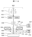
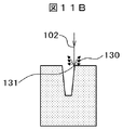
- FIG. 11A shows the basic configuration of the image pickup optical system 002 according to the third embodiment of the present invention.
- the difference from the imaging optical system 001 described in the first embodiment (see FIG. 1A) is that a detector 121 for detecting secondary electrons 120 emitted from 107 samples is added.
- secondary electrons (SE) emitted from the hole bottom of the hole formed in the sample cannot escape out of the hole, but are shown in FIG. 11B.
- the secondary electrons 130 emitted in the vicinity of the top edge 131 of the hole are detected by the detector 121.
- Example 1 When Example 1, Example 2 and Example 3 are combined, as shown in FIG. 12C, the top diameter d1: 1331, hole depth h: 1333, and bottom diameter d2: 1332 of the hole (hole) 1330 are obtained. Information necessary for management of the top diameter / bottom diameter of the hole, which was the measurement task described at the beginning, can be acquired.
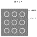
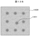
- FIG. 13A is a schematic diagram 1410 of an SE image
- FIG. 13B is a schematic diagram 1420 of a BSE image.
- the deviation of the hole center between the SE image and the BSE image indicates that the hole is not perpendicular. It is a suggestion.
- the top diameter of the hole can be measured more accurately, and information effective for managing the perpendicularity of the hole is obtained. It becomes possible.
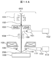
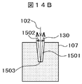
- FIG. 14A shows the basic configuration of the imaging optical system 003 according to the fourth embodiment of the present invention.
- the difference from the imaging optical system 001 described in the first embodiment (see FIG. 1) is that the imaging optical system 003 has a high angle BSE150 emitted from the sample 107 (an angle formed with the surface of the sample 107 is relatively large).
- the detector 151 for detecting the BSE 150) emitted in the direction and the image generation unit 152 for generating a high-angle BSE image are added.
- the detector 151 is emitted from the hole bottom 1503 of the hole (hole) 1501 formed in the sample 107 almost directly above, passes through the opening 1502 of the hole 1501, and is emitted out of the hole. BSE 130 is detected. An output signal from the detector 151 that detects the high-angle BSE 130 is input to the image generation unit 152 that generates a high-angle BSE image, and a digital image is generated, and is input to the calculation unit 022.
- FIG. 7B it was explained that the high-angle BSE image has no sensitivity to the hole depth. In other words, a high-angle BSE image has information on the reflected electron intensity of the hole bottom material regardless of the depth of the hole.
- the material of the hole bottom is generally indefinite.
- the signal amount changes depending on the change in the hole depth and the difference in the material of the hole bottom.
- the hole bottom material can be estimated from the signal intensity.
- FIG. 15 shows a processing flow in the calculation unit 022 when a high-angle BSE image is used together.
- the brightness of the hole bottom is calculated from the high angle BSE image input from the image generation unit 152 that generates the high angle BSE image (S160), and the material of the hole bottom is estimated from this brightness.
- a step corresponding to brightness conversion (S8032 in FIG. 8) in the case of a low-angle BSE image is necessary. If the hole bottom material cannot be determined, there is no point in performing hole depth measurement using a low-angle BSE image, and the process ends.
- the brightness of the hole bottom is calculated using the low angle BSE image input from the image generation unit 113 that generates the low angle BSE image (S162), and the brightness conversion (S163) is performed. After that, the hole depth is calculated by referring to the calibration curve of the corresponding material and acceleration voltage (S164).
- the hole depth can be measured even when the material of the hole bottom is indeterminate.
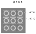
- Example 5 is a user interface for executing the present invention.
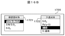
- the material designation box 1720 for designating the sidewall film material 1721 and the hole bottom material 1722 shown in FIG. A condition setting box 1730 for setting the selected optical conditions of BSE and SE and the output contents of the output information display unit 1735 is displayed on the screen of the input / output unit 024.
- FIG. 18A shows the basic configuration of the image pickup optical system according to the sixth embodiment of the present invention.
- the configurations of Examples 1 to 4 are mainly intended for hole pattern measurement, but the present embodiment is intended for a high aspect ratio groove pattern (185 in FIG. 17).
- a word line slit forming step in a 3D-NAND process corresponds to this.
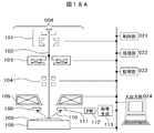
- a detector 180 divided in the azimuth direction is used as the detector 180 for low-angle BSE detection in the imaging optical system 004.
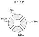
- the detector 180 for this purpose is an azimuthally divided detector 180 provided with four detection elements 180a to 180d as shown in FIG. 18B. Depending on the direction of the groove, the direction of the detector output to be used is selected.
- the imaging optical system 004 shown in FIG. 18A not only the measurement of the depth and groove width of the groove pattern 185 formed in the sample 200 as shown in FIG. 17, but also as described in the first and second embodiments. It is also possible to measure the depth and diameter of the hole pattern.
- the punch-through BSE detection which is the present invention, to the measurement of a groove pattern with a high aspect ratio.
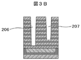
- Electron gun 102 ... Primary electron Line 103 ... Condenser lens 104 ... Deflector 105 ... Objective lens 106 ... Low-angle BSE detection annular scintillator 108 ... Stage 110 ... Low-angle BSE 111 ... Optical fiber 112 ⁇ Photomultiplier tube ⁇ 200 206, 207 ... Hole with insufficient drilling 208, 209 ... Excessive drilling 120 ... secondary electrons 121 ... secondary electron detector 122 ... image generation unit for generating a secondary electron image 130 ...
Landscapes
- Chemical & Material Sciences (AREA)
- Analytical Chemistry (AREA)
- Physics & Mathematics (AREA)
- Electromagnetism (AREA)
- General Physics & Mathematics (AREA)
- Length-Measuring Devices Using Wave Or Particle Radiation (AREA)
- Testing Or Measuring Of Semiconductors Or The Like (AREA)
Priority Applications (2)
| Application Number | Priority Date | Filing Date | Title |
|---|---|---|---|
| US15/039,527 US9852881B2 (en) | 2013-12-02 | 2014-11-19 | Scanning electron microscope system, pattern measurement method using same, and scanning electron microscope |
| KR1020167006631A KR101762219B1 (ko) | 2013-12-02 | 2014-11-19 | 주사 전자 현미경 시스템 및 그것을 이용한 패턴 계측 방법 및 주사 전자 현미경 |
Applications Claiming Priority (2)
| Application Number | Priority Date | Filing Date | Title |
|---|---|---|---|
| JP2013-249249 | 2013-12-02 | ||
| JP2013249249A JP6316578B2 (ja) | 2013-12-02 | 2013-12-02 | 走査電子顕微鏡システム及びそれを用いたパターン計測方法並びに走査電子顕微鏡 |
Publications (1)
| Publication Number | Publication Date |
|---|---|
| WO2015083548A1 true WO2015083548A1 (ja) | 2015-06-11 |
Family
ID=53273315
Family Applications (1)
| Application Number | Title | Priority Date | Filing Date |
|---|---|---|---|
| PCT/JP2014/080661 Ceased WO2015083548A1 (ja) | 2013-12-02 | 2014-11-19 | 走査電子顕微鏡システム及びそれを用いたパターン計測方法並びに走査電子顕微鏡 |
Country Status (5)
| Country | Link |
|---|---|
| US (1) | US9852881B2 (enExample) |
| JP (1) | JP6316578B2 (enExample) |
| KR (1) | KR101762219B1 (enExample) |
| TW (1) | TWI564926B (enExample) |
| WO (1) | WO2015083548A1 (enExample) |
Cited By (2)
| Publication number | Priority date | Publication date | Assignee | Title |
|---|---|---|---|---|
| WO2020075385A1 (ja) * | 2018-10-09 | 2020-04-16 | 株式会社日立製作所 | 計測装置及び試料の表面の計測方法 |
| TWI741564B (zh) * | 2019-05-08 | 2021-10-01 | 日商日立全球先端科技股份有限公司 | 圖案量測裝置及量測方法 |
Families Citing this family (40)
| Publication number | Priority date | Publication date | Assignee | Title |
|---|---|---|---|---|
| US9653257B2 (en) * | 2015-03-03 | 2017-05-16 | Kla-Tencor Corporation | Method and system for reducing charging artifacts in scanning electron microscopy images |
| JP6527799B2 (ja) * | 2015-09-25 | 2019-06-05 | 株式会社日立ハイテクノロジーズ | 荷電粒子線装置及びパターン測定装置 |
| JP6820660B2 (ja) * | 2016-01-29 | 2021-01-27 | 株式会社日立ハイテク | 荷電粒子線装置 |
| US10460903B2 (en) * | 2016-04-04 | 2019-10-29 | Kla-Tencor Corporation | Method and system for charge control for imaging floating metal structures on non-conducting substrates |
| US10816332B2 (en) | 2016-04-13 | 2020-10-27 | Hitachi High-Tech Corporation | Pattern measurement device and pattern measurement method |
| WO2018020626A1 (ja) * | 2016-07-28 | 2018-02-01 | 株式会社 日立ハイテクノロジーズ | 荷電粒子線装置 |
| JP6640057B2 (ja) * | 2016-09-14 | 2020-02-05 | 株式会社日立ハイテクノロジーズ | 電子顕微鏡装置及びそれを用いた傾斜ホールの測定方法 |
| JP2018113322A (ja) | 2017-01-11 | 2018-07-19 | 株式会社日立国際電気 | 半導体装置の製造方法、プログラムおよび基板処理装置 |
| EP4163950A1 (en) * | 2017-02-07 | 2023-04-12 | ASML Netherlands B.V. | Method and apparatus for charged particle detection |
| IL273418B2 (en) * | 2017-09-26 | 2026-01-01 | Asml Netherlands Bv | Identification of inherent properties by scattered particles |
| US11353798B2 (en) | 2017-10-13 | 2022-06-07 | Hitachi High-Technologies Corporation | Pattern measurement device and pattern measurement method |
| JP6865465B2 (ja) * | 2017-11-10 | 2021-04-28 | 株式会社日立ハイテク | パターン計測装置および計測方法 |
| JP6541161B2 (ja) * | 2017-11-17 | 2019-07-10 | 株式会社日立ハイテクサイエンス | 荷電粒子ビーム装置 |
| JP7137943B2 (ja) * | 2018-03-20 | 2022-09-15 | 株式会社日立ハイテク | 探索装置、探索方法及びプラズマ処理装置 |
| JP2019184354A (ja) | 2018-04-06 | 2019-10-24 | 株式会社日立ハイテクノロジーズ | 電子顕微鏡装置、電子顕微鏡装置を用いた検査システム及び電子顕微鏡装置を用いた検査方法 |
| JP2019185972A (ja) * | 2018-04-06 | 2019-10-24 | 株式会社日立ハイテクノロジーズ | 走査電子顕微鏡システム及びパターンの深さ計測方法 |
| JP2019211356A (ja) * | 2018-06-06 | 2019-12-12 | 株式会社日立ハイテクノロジーズ | パターン測定方法、パターン測定ツール、及びコンピュータ可読媒体 |
| US10714306B2 (en) * | 2018-06-11 | 2020-07-14 | Applied Materials Israel Ltd. | Measuring a height profile of a hole formed in non-conductive region |
| US10340116B1 (en) * | 2018-06-13 | 2019-07-02 | Applied Materials Israel Ltd. | Imaging an area that includes an upper surface and a hole |
| DE112018007843B4 (de) | 2018-09-21 | 2024-05-29 | Hitachi High-Tech Corporation | Mit einem strahl geladener teilchen arbeitende vorrichtung |
| WO2020095346A1 (ja) * | 2018-11-05 | 2020-05-14 | 株式会社 日立ハイテクノロジーズ | パターン計測方法、計測システム、及びコンピュータ可読媒体 |
| JP7091263B2 (ja) * | 2019-01-22 | 2022-06-27 | 株式会社日立ハイテク | 電子顕微鏡及び3次元構造の深さ算出方法 |
| JP7199290B2 (ja) | 2019-04-08 | 2023-01-05 | 株式会社日立ハイテク | パターン断面形状推定システム、およびプログラム |
| US11139142B2 (en) * | 2019-05-23 | 2021-10-05 | Applied Materials, Inc. | High-resolution three-dimensional profiling of features in advanced semiconductor devices in a non-destructive manner using electron beam scanning electron microscopy |
| JP7149906B2 (ja) | 2019-08-07 | 2022-10-07 | 株式会社日立ハイテク | 走査電子顕微鏡及びパタン計測方法 |
| KR102771899B1 (ko) * | 2019-09-03 | 2025-02-25 | 삼성전자주식회사 | 주사 전자 현미경 장치 및 그의 동작 방법 |
| CN110751622B (zh) * | 2019-09-05 | 2022-07-15 | 长江存储科技有限责任公司 | 半导体结构的检测方法及其检测装置 |
| US10943763B1 (en) * | 2019-09-24 | 2021-03-09 | Applied Materials, Inc. | Use of electron beam scanning electron microscopy for characterization of a sidewall occluded from line-of-sight of the electron beam |
| CN112967941B (zh) * | 2019-12-12 | 2022-04-26 | 长鑫存储技术有限公司 | 电容孔倾斜检测与反馈的方法、系统及存储介质 |
| US11056404B1 (en) * | 2019-12-18 | 2021-07-06 | Applied Materials Israel Ltd. | Evaluating a hole formed in an intermediate product |
| US11335608B2 (en) | 2020-04-15 | 2022-05-17 | Kla Corporation | Electron beam system for inspection and review of 3D devices |
| JP2022015476A (ja) | 2020-07-09 | 2022-01-21 | キオクシア株式会社 | 位置ずれ計測装置、位置ずれ計測方法、及び位置ずれ計測プログラム |
| US12176252B2 (en) | 2021-01-14 | 2024-12-24 | Changxin Memory Technologies, Inc. | Method and device for predicting inclination angle, and method and device for monitoring etching device |
| CN112713113B (zh) * | 2021-01-14 | 2022-05-24 | 长鑫存储技术有限公司 | 倾斜角度预测方法及装置、设备监控方法、介质及设备 |
| JP2022112137A (ja) * | 2021-01-21 | 2022-08-02 | 株式会社日立ハイテク | 荷電粒子ビーム装置 |
| JP2022170466A (ja) * | 2021-04-28 | 2022-11-10 | 株式会社日立ハイテク | 荷電粒子ビームシステム |
| US20240240937A1 (en) * | 2021-05-28 | 2024-07-18 | Hitachi High-Tech Corporation | Depth Measurement Device, Depth Measurement System, and Depth Index Calculation Method |
| CN113466277B (zh) * | 2021-06-25 | 2022-05-10 | 长江存储科技有限责任公司 | 测试样品的制备方法及测试样品 |
| US11921063B2 (en) * | 2021-07-21 | 2024-03-05 | Applied Materials Israel Ltd. | Lateral recess measurement in a semiconductor specimen |
| CN113725113B (zh) * | 2021-08-30 | 2023-11-10 | 长江存储科技有限责任公司 | 半导体器件测量方法及装置 |
Citations (8)
| Publication number | Priority date | Publication date | Assignee | Title |
|---|---|---|---|---|
| JPH04149944A (ja) * | 1990-10-12 | 1992-05-22 | Hitachi Ltd | 走査形電子顕微鏡、及び走査形電子顕微鏡による試料像形成方法 |
| JPH06310075A (ja) * | 1993-04-27 | 1994-11-04 | Hitachi Ltd | 走査型電子顕微鏡 |
| JP2002110079A (ja) * | 2000-09-29 | 2002-04-12 | Hitachi Ltd | 電子線装置 |
| JP2003157790A (ja) * | 2001-11-20 | 2003-05-30 | Advantest Corp | 微細凹凸量測定装置及び走査型電子顕微鏡 |
| JP2010175249A (ja) * | 2009-01-27 | 2010-08-12 | Hitachi High-Technologies Corp | 試料高さ測定方法及び試料高さ測定装置 |
| JP2013045500A (ja) * | 2011-08-22 | 2013-03-04 | Hitachi High-Technologies Corp | 荷電粒子線装置 |
| JP2013089514A (ja) * | 2011-10-20 | 2013-05-13 | Hitachi High-Technologies Corp | 走査電子顕微鏡 |
| JP2013134879A (ja) * | 2011-12-26 | 2013-07-08 | Toshiba Corp | 信号処理方法および信号処理装置 |
Family Cites Families (4)
| Publication number | Priority date | Publication date | Assignee | Title |
|---|---|---|---|---|
| US5412210A (en) * | 1990-10-12 | 1995-05-02 | Hitachi, Ltd. | Scanning electron microscope and method for production of semiconductor device by using the same |
| JP3749107B2 (ja) * | 1999-11-05 | 2006-02-22 | ファブソリューション株式会社 | 半導体デバイス検査装置 |
| WO2007067296A2 (en) * | 2005-12-02 | 2007-06-14 | Alis Corporation | Ion sources, systems and methods |
| WO2012039206A1 (ja) * | 2010-09-25 | 2012-03-29 | 株式会社日立ハイテクノロジーズ | 荷電粒子ビーム顕微鏡 |
-
2013
- 2013-12-02 JP JP2013249249A patent/JP6316578B2/ja active Active
-
2014
- 2014-11-05 TW TW103138407A patent/TWI564926B/zh active
- 2014-11-19 US US15/039,527 patent/US9852881B2/en active Active
- 2014-11-19 KR KR1020167006631A patent/KR101762219B1/ko active Active
- 2014-11-19 WO PCT/JP2014/080661 patent/WO2015083548A1/ja not_active Ceased
Patent Citations (8)
| Publication number | Priority date | Publication date | Assignee | Title |
|---|---|---|---|---|
| JPH04149944A (ja) * | 1990-10-12 | 1992-05-22 | Hitachi Ltd | 走査形電子顕微鏡、及び走査形電子顕微鏡による試料像形成方法 |
| JPH06310075A (ja) * | 1993-04-27 | 1994-11-04 | Hitachi Ltd | 走査型電子顕微鏡 |
| JP2002110079A (ja) * | 2000-09-29 | 2002-04-12 | Hitachi Ltd | 電子線装置 |
| JP2003157790A (ja) * | 2001-11-20 | 2003-05-30 | Advantest Corp | 微細凹凸量測定装置及び走査型電子顕微鏡 |
| JP2010175249A (ja) * | 2009-01-27 | 2010-08-12 | Hitachi High-Technologies Corp | 試料高さ測定方法及び試料高さ測定装置 |
| JP2013045500A (ja) * | 2011-08-22 | 2013-03-04 | Hitachi High-Technologies Corp | 荷電粒子線装置 |
| JP2013089514A (ja) * | 2011-10-20 | 2013-05-13 | Hitachi High-Technologies Corp | 走査電子顕微鏡 |
| JP2013134879A (ja) * | 2011-12-26 | 2013-07-08 | Toshiba Corp | 信号処理方法および信号処理装置 |
Cited By (2)
| Publication number | Priority date | Publication date | Assignee | Title |
|---|---|---|---|---|
| WO2020075385A1 (ja) * | 2018-10-09 | 2020-04-16 | 株式会社日立製作所 | 計測装置及び試料の表面の計測方法 |
| TWI741564B (zh) * | 2019-05-08 | 2021-10-01 | 日商日立全球先端科技股份有限公司 | 圖案量測裝置及量測方法 |
Also Published As
| Publication number | Publication date |
|---|---|
| KR20160046837A (ko) | 2016-04-29 |
| KR101762219B1 (ko) | 2017-07-27 |
| US9852881B2 (en) | 2017-12-26 |
| TWI564926B (zh) | 2017-01-01 |
| TW201532101A (zh) | 2015-08-16 |
| JP6316578B2 (ja) | 2018-04-25 |
| US20160379798A1 (en) | 2016-12-29 |
| JP2015106530A (ja) | 2015-06-08 |
Similar Documents
| Publication | Publication Date | Title |
|---|---|---|
| JP6316578B2 (ja) | 走査電子顕微鏡システム及びそれを用いたパターン計測方法並びに走査電子顕微鏡 | |
| CN109765254B (zh) | 图案测量装置以及测量方法 | |
| US9536700B2 (en) | Sample observation device | |
| WO2017051621A1 (ja) | 荷電粒子線装置及びパターン測定装置 | |
| US11211226B2 (en) | Pattern cross-sectional shape estimation system and program | |
| US20120217392A1 (en) | Pattern-height measuring apparatus and pattern-height measuring method | |
| JPWO2017179138A1 (ja) | パターン計測装置およびパターン計測方法 | |
| US11545336B2 (en) | Scanning electron microscopy system and pattern depth measurement method | |
| US20210404801A1 (en) | Pattern Measurement Method, Measurement System, and Computer-Readable Medium | |
| JP2015146283A (ja) | 荷電粒子線装置及び画像生成方法 | |
| JP5932428B2 (ja) | 走査電子顕微鏡 | |
| US11302513B2 (en) | Electron microscope apparatus, inspection system using electron microscope apparatus, and inspection method using electron microscope apparatus | |
| US10903041B2 (en) | Pattern measuring method, pattern measuring tool and computer readable medium | |
| US11443914B2 (en) | Charged-particle beam device and cross-sectional shape estimation program | |
| JPH08329875A (ja) | 走査型電子顕微鏡及びその試料像表示方法 | |
| JP5619118B2 (ja) | 荷電粒子線装置 | |
| KR102700926B1 (ko) | 하전 입자선 장치 | |
| JP2016139531A (ja) | 試料の観察、検査、測定方法、及び走査電子顕微鏡 |
Legal Events
| Date | Code | Title | Description |
|---|---|---|---|
| 121 | Ep: the epo has been informed by wipo that ep was designated in this application |
Ref document number: 14868670 Country of ref document: EP Kind code of ref document: A1 |
|
| ENP | Entry into the national phase |
Ref document number: 20167006631 Country of ref document: KR Kind code of ref document: A |
|
| WWE | Wipo information: entry into national phase |
Ref document number: 15039527 Country of ref document: US |
|
| NENP | Non-entry into the national phase |
Ref country code: DE |
|
| 122 | Ep: pct application non-entry in european phase |
Ref document number: 14868670 Country of ref document: EP Kind code of ref document: A1 |