WO2015016202A1 - 伝導性フィラー及びその製造方法、並びに伝導性ペースト及びその製造方法 - Google Patents
伝導性フィラー及びその製造方法、並びに伝導性ペースト及びその製造方法 Download PDFInfo
- Publication number
- WO2015016202A1 WO2015016202A1 PCT/JP2014/069901 JP2014069901W WO2015016202A1 WO 2015016202 A1 WO2015016202 A1 WO 2015016202A1 JP 2014069901 W JP2014069901 W JP 2014069901W WO 2015016202 A1 WO2015016202 A1 WO 2015016202A1
- Authority
- WO
- WIPO (PCT)
- Prior art keywords
- conductive filler
- copper alloy
- alloy powder
- conductive
- carbon
- Prior art date
Links
Images


Classifications
-
- C—CHEMISTRY; METALLURGY
- C22—METALLURGY; FERROUS OR NON-FERROUS ALLOYS; TREATMENT OF ALLOYS OR NON-FERROUS METALS
- C22C—ALLOYS
- C22C9/00—Alloys based on copper
-
- B—PERFORMING OPERATIONS; TRANSPORTING
- B22—CASTING; POWDER METALLURGY
- B22F—WORKING METALLIC POWDER; MANUFACTURE OF ARTICLES FROM METALLIC POWDER; MAKING METALLIC POWDER; APPARATUS OR DEVICES SPECIALLY ADAPTED FOR METALLIC POWDER
- B22F1/00—Metallic powder; Treatment of metallic powder, e.g. to facilitate working or to improve properties
- B22F1/06—Metallic powder characterised by the shape of the particles
- B22F1/068—Flake-like particles
-
- B—PERFORMING OPERATIONS; TRANSPORTING
- B22—CASTING; POWDER METALLURGY
- B22F—WORKING METALLIC POWDER; MANUFACTURE OF ARTICLES FROM METALLIC POWDER; MAKING METALLIC POWDER; APPARATUS OR DEVICES SPECIALLY ADAPTED FOR METALLIC POWDER
- B22F1/00—Metallic powder; Treatment of metallic powder, e.g. to facilitate working or to improve properties
- B22F1/10—Metallic powder containing lubricating or binding agents; Metallic powder containing organic material
-
- B—PERFORMING OPERATIONS; TRANSPORTING
- B22—CASTING; POWDER METALLURGY
- B22F—WORKING METALLIC POWDER; MANUFACTURE OF ARTICLES FROM METALLIC POWDER; MAKING METALLIC POWDER; APPARATUS OR DEVICES SPECIALLY ADAPTED FOR METALLIC POWDER
- B22F1/00—Metallic powder; Treatment of metallic powder, e.g. to facilitate working or to improve properties
- B22F1/16—Metallic particles coated with a non-metal
-
- C—CHEMISTRY; METALLURGY
- C09—DYES; PAINTS; POLISHES; NATURAL RESINS; ADHESIVES; COMPOSITIONS NOT OTHERWISE PROVIDED FOR; APPLICATIONS OF MATERIALS NOT OTHERWISE PROVIDED FOR
- C09D—COATING COMPOSITIONS, e.g. PAINTS, VARNISHES OR LACQUERS; FILLING PASTES; CHEMICAL PAINT OR INK REMOVERS; INKS; CORRECTING FLUIDS; WOODSTAINS; PASTES OR SOLIDS FOR COLOURING OR PRINTING; USE OF MATERIALS THEREFOR
- C09D5/00—Coating compositions, e.g. paints, varnishes or lacquers, characterised by their physical nature or the effects produced; Filling pastes
- C09D5/24—Electrically-conducting paints
-
- C—CHEMISTRY; METALLURGY
- C22—METALLURGY; FERROUS OR NON-FERROUS ALLOYS; TREATMENT OF ALLOYS OR NON-FERROUS METALS
- C22C—ALLOYS
- C22C1/00—Making non-ferrous alloys
- C22C1/04—Making non-ferrous alloys by powder metallurgy
- C22C1/0425—Copper-based alloys
-
- C—CHEMISTRY; METALLURGY
- C23—COATING METALLIC MATERIAL; COATING MATERIAL WITH METALLIC MATERIAL; CHEMICAL SURFACE TREATMENT; DIFFUSION TREATMENT OF METALLIC MATERIAL; COATING BY VACUUM EVAPORATION, BY SPUTTERING, BY ION IMPLANTATION OR BY CHEMICAL VAPOUR DEPOSITION, IN GENERAL; INHIBITING CORROSION OF METALLIC MATERIAL OR INCRUSTATION IN GENERAL
- C23C—COATING METALLIC MATERIAL; COATING MATERIAL WITH METALLIC MATERIAL; SURFACE TREATMENT OF METALLIC MATERIAL BY DIFFUSION INTO THE SURFACE, BY CHEMICAL CONVERSION OR SUBSTITUTION; COATING BY VACUUM EVAPORATION, BY SPUTTERING, BY ION IMPLANTATION OR BY CHEMICAL VAPOUR DEPOSITION, IN GENERAL
- C23C16/00—Chemical coating by decomposition of gaseous compounds, without leaving reaction products of surface material in the coating, i.e. chemical vapour deposition [CVD] processes
- C23C16/06—Chemical coating by decomposition of gaseous compounds, without leaving reaction products of surface material in the coating, i.e. chemical vapour deposition [CVD] processes characterised by the deposition of metallic material
-
- H—ELECTRICITY
- H01—ELECTRIC ELEMENTS
- H01B—CABLES; CONDUCTORS; INSULATORS; SELECTION OF MATERIALS FOR THEIR CONDUCTIVE, INSULATING OR DIELECTRIC PROPERTIES
- H01B1/00—Conductors or conductive bodies characterised by the conductive materials; Selection of materials as conductors
- H01B1/20—Conductive material dispersed in non-conductive organic material
- H01B1/22—Conductive material dispersed in non-conductive organic material the conductive material comprising metals or alloys
-
- C—CHEMISTRY; METALLURGY
- C22—METALLURGY; FERROUS OR NON-FERROUS ALLOYS; TREATMENT OF ALLOYS OR NON-FERROUS METALS
- C22C—ALLOYS
- C22C9/00—Alloys based on copper
- C22C9/06—Alloys based on copper with nickel or cobalt as the next major constituent
Definitions
- the present invention relates to a conductive paste such as an electrically conductive (conductive) paste or a thermally conductive paste, and a method for manufacturing the same. Moreover, it is related with the conductive filler for forming the said conductive paste, and its manufacturing method.
- a conductive paste such as an electrically conductive (conductive) paste or a thermally conductive paste
- Various conductive pastes containing copper powder and binder resin are known.
- Examples of such a conductive paste include a conductive paste used as a circuit and a conductive adhesive, a heat conductive paste, and the like.
- the carbon fibers tend to aggregate when the carbon fibers are dispersed or coated.
- Patent Document 1 discloses a method of arranging a metal catalyst on a metal surface and producing carbon nanotubes using the metal catalyst. Since the carbon nanotubes are bonded to the metal surface, the carbon nanotubes hardly aggregate.
- Patent Document 1 The method described in Patent Document 1 was merely a method for producing carbon nanotubes on a metal substrate. That is, conventionally, it has been difficult to uniformly disperse carbon materials such as carbon nanotubes and carbon fibers in a composition containing a metal powder such as a conductive paste or a heat conductive paste and a binder resin. Therefore, it has been difficult to develop high conductivity and high thermal conductivity.
- a metal powder such as a conductive paste or a heat conductive paste and a binder resin. Therefore, it has been difficult to develop high conductivity and high thermal conductivity.
- An object of the present invention is to provide a conductive paste and a method for manufacturing the same, which can effectively improve conductivity and thermal conductivity. Moreover, it is providing the conductive filler for forming the said conductive paste, and its manufacturing method.
- the conductive filler according to the present invention is a composite comprising a copper alloy powder containing at least one transition metal belonging to Groups 8 to 10 of the periodic table, and a carbon allotrope covering the surface of the copper alloy powder. Particles.
- the carbon allotrope may be grown from a transition metal composed of Groups 8 to 10 of the periodic table in the copper alloy powder.
- the copper alloy powder is preferably flaky.
- the composite particles are composite flake particles in which the carbon allotrope covers the surface of the copper alloy powder.
- the content of the transition metal in the copper alloy powder is preferably 0.3 to 6.0% by weight with respect to 100% by weight of the copper alloy powder.
- iron or cobalt is preferably used as the transition metal. More preferably, cobalt is used.
- the carbon allotrope is adhered to the surface of the copper alloy powder in a range of greater than 0% by weight and 3% by weight or less with respect to 100% by weight of the copper alloy powder.
- the carbon allotrope is preferably carbon nanofiber, and in this case, it is desirable that one end of the carbon nanofiber is bonded to the copper alloy powder.
- the conductive paste according to the present invention includes the conductive filler according to the present invention and a binder resin.
- the binder resin is preferably at least one resin selected from the group consisting of epoxy resins, polyester resins, urethane resins, phenol resins, and imide resins.
- the conductive paste of the present invention may be an electrically conductive paste, that is, a conductive paste, or a heat conductive paste.
- the method for producing a conductive filler of the present invention comprises a step of preparing a copper alloy powder containing at least one transition metal belonging to Groups 8 to 10 of the periodic table, and contacting a carbon source with the surface of the copper alloy powder. And obtaining a conductive filler.
- the step of preparing the copper alloy powder is performed by an atomizing method.
- the step of obtaining a conductive filler by bringing a carbon source into contact with the surface of the copper alloy powder is in the order of CVD treatment, flaking treatment, and re-CVD treatment. It is a process of obtaining a conductive filler by processing. Carbon fibers are produced at 400 ° C to 750 ° C.
- the step of obtaining a conductive filler by bringing a carbon source into contact with the surface of the copper alloy powder is conducted by treating in the order of CVD treatment and heat treatment. This is a step of obtaining a filler.
- the heat treatment is performed in a temperature atmosphere of 750 ° C. to 1000 ° C. in an inert gas atmosphere.
- the step of obtaining a conductive filler by bringing a carbon source into contact with the surface of the copper alloy powder comprises subjecting the copper alloy powder to carbon at 300 ° C. to 400 ° C. It is a step of contacting the contained gas.
- a sintering inhibitor is added and mixed before the step of obtaining a conductive filler by bringing a carbon source into contact with the surface of the copper alloy powder.
- the method further includes a step.
- the step of producing a conductive filler according to the method for producing a conductive filler according to the present invention the conductive filler and the binder resin are mixed, and then kneaded. Obtaining a conductive paste.
- the conductive filler and conductive paste according to the present invention since the surface of the copper alloy powder is covered with the carbon allotrope, the conductive filler and conductive paste exhibiting high conductivity and high thermal conductivity are provided. Is possible.
- FIG. 1 is a diagram showing a heat profile as an example of a method for producing composite particles.
- FIG. 2 is a diagram showing a heat profile of the re-CVD process.
- FIG. 3 is a diagram showing specific resistances of the conductive paste prepared in the example and pastes made of various materials.
- FIG. 4 is a view showing an electron micrograph of the composite particles prepared in Example 1 at a magnification of 8000 times.
- FIG. 5 is a view showing an electron micrograph of the composite particles prepared in Example 2 at a magnification of 4000 times.
- 6 is a view showing an electron micrograph of the composite particles prepared in Example 2 at a magnification of 20000 times.
- FIG. 1 is a diagram showing a heat profile as an example of a method for producing composite particles.
- FIG. 2 is a diagram showing a heat profile of the re-CVD process.
- FIG. 3 is a diagram showing specific resistances of the conductive paste prepared in the example and pastes made of various materials.
- FIG. 7 is a view showing an electron micrograph of the composite particles prepared in Example 3 at a magnification of 8000 times.
- FIG. 8 is a view showing an electron micrograph of the composite particles prepared in Example 4 at a magnification of 20000 times.
- FIG. 9 is an electron micrograph of the composite particles prepared in Example 5 at a magnification of 20000 times.
- FIG. 10 is a view showing an electron micrograph of the composite particles prepared in Example 6 at a magnification of 8000 times.
- FIG. 11 is a diagram showing a heat profile when a heat treatment step is provided after the CVD step.
- 12 is a view showing an electron micrograph of the composite particles prepared in Example 11 at a magnification of 20000 times.
- FIG. 13 shows an electron micrograph of the composite particles prepared in Example 11 at a magnification of 2000 times.
- FIG. 14 is a diagram showing the specific resistance of the conductive paste prepared in the example and the paste made of various materials without compression.
- Conductive filler 1-1 Copper Alloy Powder
- the conductive filler according to the present invention includes a copper alloy powder containing at least one transition metal belonging to Groups 8 to 10 of the periodic table, and a carbon allotrope covering the surface of the copper alloy powder.
- the filler is composed of composite particles.
- the composite particles may be composite flake particles in which the carbon allotrope covers the flaky copper alloy powder.
- the conductive paste which concerns on this invention contains the said conductive filler and binder resin.
- the carbon allotrope covers the surface of the copper alloy powder, not only when the carbon allotrope completely covers the surface of the copper alloy powder by a scanning electron microscope, Although it cannot be confirmed that the surface of the copper alloy powder is only partially covered by a scanning electron microscope, it is actually used to include the case where the carbon allotrope covers the surface of the copper alloy powder at the nano level. Shall be. Note that the carbon allotrope covers the surface of the copper alloy powder at the nano level can be confirmed by an Auger electron spectrometer.
- the transition metal belonging to Group 8 to Group 10 of the periodic table is not particularly limited, and preferably iron, nickel, cobalt, or palladium. Especially, since catalytic activity is high, iron, nickel, or cobalt is desirable, and iron or cobalt is more preferable. More preferably, it is cobalt. However, a plurality of transition metals may be used in combination.
- the copper alloy powder can be obtained, for example, by pulverizing by an atomizing method.
- the average particle diameter of the copper alloy powder is not particularly limited, but is preferably 0.1 ⁇ m to 50 ⁇ m, more preferably 0.1 ⁇ m to 20 ⁇ m, and still more preferably 0.1 ⁇ m to 5 ⁇ m.
- the average particle diameter of the copper alloy powder is within the above preferred range, a conductive paste excellent in electrical conductivity and thermal conductivity can be provided more reliably according to the present invention.
- the copper alloy powder may have a spherical shape, but preferably has a flake shape with an aspect ratio larger than 1. Therefore, it is preferable to flatten the copper alloy powder after atomization, for example, by ball mill treatment, treatment using a cold spray method or aerosol deposition method for powder processing, or the like. When processed into a flake shape with a ball mill or the like, it is preferable to mix flake powder having a long side of 5 to 50 ⁇ m. These flake powders can also be obtained by ball milling atomized powder of about 1 to 5 ⁇ m.
- the copper alloy powder be cleaned with an etching solution or the like before the carbon allotrope is attached to the surface by the CVD process described later.
- the total content of the transition metal is preferably 0.1 to 10.0% by weight, more preferably 0.3 to 6.0% by weight in 100% by weight of the copper alloy powder. More preferably, it is 0.3 to 1.0% by weight.
- the content ratio of the transition metal is within the above range, according to the present invention, a conductive filler and a conductive paste excellent in electrical conductivity and thermal conductivity can be provided more reliably.
- the conductive filler according to the present invention is a composite particle in which a carbon allotrope is attached to the copper alloy powder so as to cover the surface of the copper alloy powder.
- Such composite particles can be formed by a CVD method in which a carbon source is brought into contact with the surface of the copper alloy powder at 400 ° C. to 750 ° C. That is, it is desirable to produce a carbon allotrope on the surface of the copper alloy powder by the CVD method.
- Examples of the carbon allotrope include one or more graphene laminates, carbon nanofibers, and the like.
- a carbon nanofiber with a small fiber diameter is more preferable.
- the carbon nanofiber is a carbon fiber having a fiber diameter of about 5 to 500 nm.
- sea urchin-shaped composite particles are called spiny particles.
- spiny particles it is more desirable that the density of the carbon nanofiber is high.
- the composite particles having the above-mentioned spiny particle shape surprisingly, it is confirmed that when the adjacent composite particles are brought into contact with each other, the conductivity is much higher than when the copper alloy particles are in contact with each other. It has been. That is, the conductivity is further enhanced when the above-mentioned spiny particle-shaped composite particles are brought into contact with each other rather than the respective conductivity of the copper alloy and carbon nanofibers constituting the composite particle.
- the carbon nanofiber has an sp2 structure and has been confirmed to have conductivity, but it has not been confirmed whether or not it exhibits a very high conductivity like SWCNT.
- the conductive filler which is the composite particle of the present invention, it is considered that it is preferable to form shorter fibers on the surface of the copper alloy powder when the conductivity in the length direction of the CNT carbon nanoparticles is lower. Even in this case, the carbon nanofibers are entangled between adjacent composite particles, and the conductivity can be effectively increased.
- the length of the carbon nanofiber is preferably 0.01 ⁇ m to 5.0 ⁇ m, more preferably 0.01 ⁇ m to 0 ⁇ m. Desirably about 2 ⁇ m.
- the amount of carbon allotrope attached to the copper alloy powder is preferably within a certain range. This is because the carbon allotrope is used to reduce the contact resistance between the copper particles, although the conductivity is inferior to copper.
- the adhesion amount of the carbon allotrope to the copper alloy powder in the present invention is not particularly limited, but is preferably greater than 0% by weight and 4.0% by weight or less with respect to 100% by weight of the copper alloy powder, and 0% by weight. It is more preferably 3.0% by weight or less, more preferably 0% by weight or more and 1.5% by weight or less, more preferably 0% by weight or more and 1.0% by weight or less. Is most preferred. This is because if the carbon allotrope is attached to the copper alloy powder too much, the carbon allotrope having a conductivity lower than that of the copper alloy particles may lower the conductivity.
- a carbon-containing compound having 1 to 30 carbon atoms, preferably 1 to 7 carbon atoms, more preferably 1 to 4 carbon atoms, and still more preferably 1 or 2 carbon atoms can be used.
- examples of such compounds include carbon monoxide, hydrocarbons, and alcohols.
- the hydrocarbon a saturated hydrocarbon such as methane, ethane, or propane, or an unsaturated hydrocarbon such as ethylene or acetylene can be used as appropriate.
- the alcohol methanol or ethanol can be used as appropriate.
- the carbon source is desirably a material that is a gas at a high temperature of about 300 ° C. or higher. Thereby, it becomes easy to produce carbon fibers by a gas phase reaction.
- the dimensions of the composite particles may be appropriately adjusted depending on the application method and application of the intended conductive paste.
- the particle size of the composite particles is preferably about 1 ⁇ m to 50 ⁇ m.
- the average particle diameter of the composite particles is desirably 20 ⁇ m or less. Furthermore, in the conductive paste used for screen printing, the average particle size of the composite particles is preferably about 0.5 ⁇ m to 10 ⁇ m. When flaky particles are mixed, the flaky particles are preferably about 1 ⁇ m to 50 ⁇ m.
- the average particle size of the composite particles in the present invention may be appropriately selected according to the purpose of use and the coating method.
- the surface of the copper alloy powder is formed by a CVD method.
- a carbon source may be contacted.
- the copper alloy powder is obtained by an atomizing method as described above. Therefore, it is possible to obtain a copper alloy powder with little variation in average particle diameter.
- the copper alloy powder may be heat-treated at 400 to 800 ° C. for several minutes to several thousand minutes in an antioxidant atmosphere, for example, so that catalyst nanoparticles are deposited and dispersed in the copper alloy particles and on the surface. Desirable (catalyst precipitation step).
- an apparatus in which the powder flows and is uniformly processed like a rotary kiln (rotary furnace).
- the amount of particles added is desirably 0.05 to 2.0% by weight with respect to the copper alloy powder. More preferably, it is 0.1% by weight to 1.0% by weight.
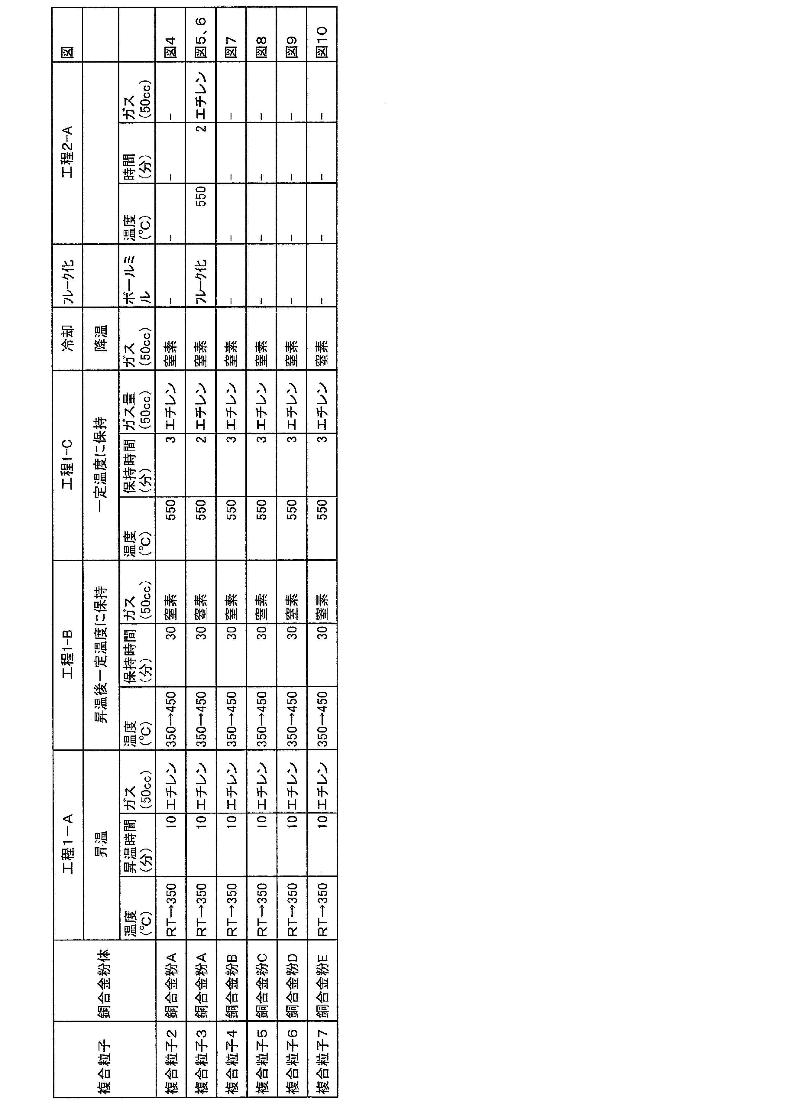
- FIG. 1 shows a heat profile as an example of a method for producing a conductive filler that is a composite particle according to the present invention.
- the shaded portion is treated in an ethylene gas atmosphere, and the other portions are treated in a nitrogen gas atmosphere.
- Step 1-A shown in FIG. 1 includes a step of bringing copper powder into contact with ethylene gas at 300 to 400 ° C. (aggregation prevention step).
- step 1-B the nanocatalyst is deposited in the copper powder and on the surface of the copper powder by being kept at 400 to 650 ° C. in an inert gas (catalyst deposition step).
- step 1-C a carbon allotrope is generated from the nanocatalyst (carbon generation step).
- Step 1-A by bringing the copper powder into contact with ethylene gas at a low temperature (300 to 400 ° C.), aggregation of the powder in Step 1-B (sintering by placing the copper powder at a high temperature for a long time) can be prevented.
- a low temperature 300 to 400 ° C.
- addition of Aerosil as a nano-sized powder, mixing, kneading as necessary, and use as a spacer also prevents aggregation of the copper alloy powder at high temperature. be able to.
- the dispersibility of the above-mentioned Aerosil is good, and the addition does not affect the conductivity of the conductive paste.
- the powder is dispersed (jet mill, ball mill, etc.) after the catalyst precipitation step (step 1-B), and the carbon generation step (step 1-C) is performed separately in the next step.
- the powder may be processed into flakes with a ball mill or the like, and a carbon generation step (step 2-A shown in FIG. 2) may be performed in the next step.
- a carbon generation step step 2-A shown in FIG. 2 may be performed in the next step. In this way, composite flake particles can be obtained by processing in the order of CVD treatment, flaking treatment, and re-CVD treatment.
- the copper alloy powder is washed with a nital solution (nitric acid 3 wt% / ethanol solution) or the like, and further washed with ethanol and dried. It is desirable to provide it.
- a nital solution nitric acid 3 wt% / ethanol solution
- a heat treatment step (step 3-A) can be provided in an inert gas atmosphere after steps 1-A to 1-C.
- Step 3-A the crystallinity of the carbon allotrope is improved, the conductivity of the carbon allotrope is improved, and the nanocatalyst to which the carbon allotrope is attached further grows to increase the concentration of the catalyst on the copper alloy particle surface. For this reason, it is preferable because the conductivity when the obtained composite particles are kneaded and pasted with a binder resin can be further enhanced.
- the inert gas is not particularly limited, but nitrogen gas and argon gas are preferably used.
- the heat treatment step (step 3-A) is preferably performed at a higher temperature than steps 1-A to 1-C. More preferably, it is in the range of 750 ° C to 1000 ° C.
- the step 3-A may be performed separately from the steps 1-A to 1-C.
- the conductive paste according to the present invention is obtained by mixing and kneading a conductive filler, which is a composite particle obtained as described above, and a binder resin. It does not specifically limit as binder resin, The appropriate
- thermosetting resin As the binder resin used for the conductive paste, polyester resin, acrylic resin, butyral resin, or the like can be used.
- Thermoplastic resins such as thermoplastic polyimide can also be used.
- thermosetting resin it is desirable to use a thermosetting resin.
- thermosetting resin various epoxy resins, polyester resins, urethane resins, phenol resins, thermosetting polyimides and the like can be used as the thermosetting resin, and a curing agent may be contained.
- the conductive paste when using a thermoplastic resin, you may make the conductive paste contain the hardening
- curing agents include amine-based epoxy curing agents, acid anhydride-based epoxy curing agents, isocyanate-based curing agents, and imidazole-based curing agents. These resins may contain a solvent.
- the blending ratio of the binder resin is not particularly limited, but is preferably 10 to 35 parts by mass with respect to 100 parts by mass of the composite particles.
- thermosetting resin or a thermoplastic resin When a thermosetting resin or a thermoplastic resin is used, the amount of these resins added is 10 to 35 parts by mass with respect to 100 parts by mass of the composite particles in a weight ratio after the paste is dried or cured. Is desirable. More preferably, the thermosetting resin or thermoplastic resin is contained in an amount of 10 to 20 parts by mass with respect to 100 parts by mass of the composite particles.
- the binder resin may be used alone or in combination of two or more.
- an inorganic filler other than a carbon material such as silica or calcium carbonate may be added to the conductive paste in order to adjust the thixotropy.
- various coupling agents may be added to improve adhesion.
- the method for producing the conductive paste is not particularly limited, and in addition to the composite particles and the binder resin, if necessary, other additives such as the additive, solvent, and reducing agent may be mixed by an appropriate method. Good.
- the conductive filler, the resin, and other additives can be mixed and then kneaded using a dissolver or a three-roll mill.
- a three-roll mill it is desirable that the roll gap be larger than the primary particle size of the filler and kneading. Thereby, a more uniform conductive paste can be obtained.
- the fibrous carbon allotrope may be broken and shortened during kneading. Further, a small amount may adhere to the nanoprecipitation particles consisting of Groups 8 to 10 of the periodic table in a shorter state. This is because the contact between the composite particles is conducted in the carbon allotrope portion in a shortened state, so that it is possible to prevent the adverse effects of copper oxidation as in the case where copper is in direct contact. .
- the conductive paste of the present invention can be suitably used as various electrically conductive pastes used for forming conductive adhesives, conductive patterns, and the like, that is, conductive pastes.
- the composite particles contain copper alloy powder and carbon allotrope, the composite particles are excellent in thermal conductivity, and therefore can be suitably used as a thermal conductive paste.
- the conductive paste according to the present invention includes a conductive filler that is a composite particle in which the carbon allotrope covers the surface of the copper alloy powder containing the specific transition metal, and a binder resin, it has excellent electrical conductivity and heat. Expresses conductivity. In particular, when the carbon allotrope is a carbon nanofiber, the carbon nanofibers are entangled between adjacent composite particles, and the contact resistance is significantly reduced. Therefore, electrical conductivity can be improved more than the original copper alloy powder.
- Copper alloy powder was produced by a high-pressure water atomization method, and classified into copper alloy powder having an average particle size of 3 ⁇ m by an air classifier.
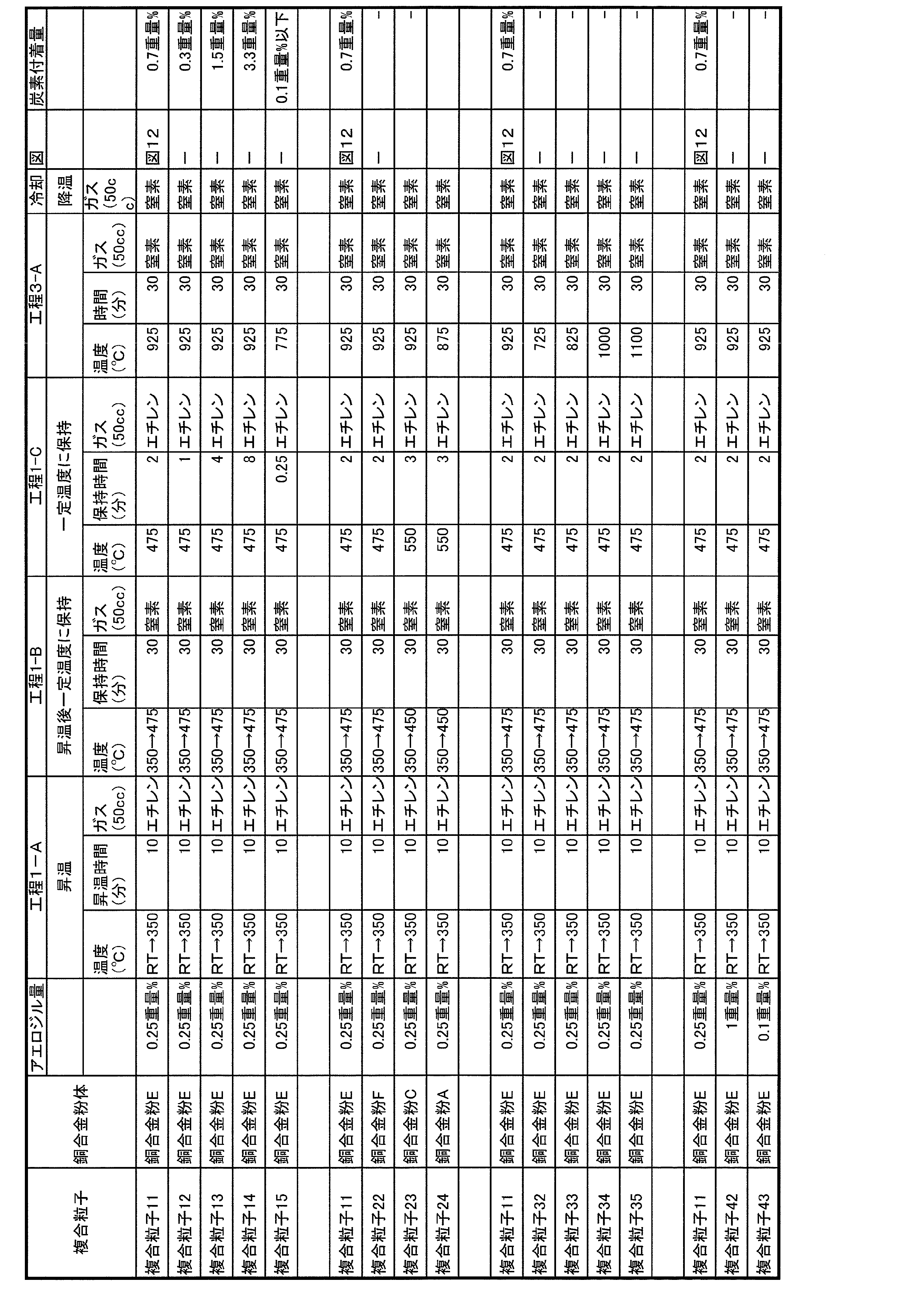
- copper alloy powders A to F shown in Table 1 below were prepared.
- Table 1 below shows the alloy components of copper alloy powders A to F and the average particle diameter.
- Aerosil 300 manufactured by Nippon Aerosil Co., Ltd. was used as Aerosil. Aerosil was added to and mixed with copper alloy powders A, C, E, and F as a pretreatment in step 1-A when producing composite particles 11 to 15, 22 to 24, 32 to 35.42, and 43.
- the copper carbon fiber spiny particles obtained in the steps 1-A, 1-B, and 1-C were further subjected to ball mill treatment, and then re-CVD treatment was performed as shown in FIG. .
- re-CVD treatment was performed as shown in FIG. .
- FIG. 2 in the re-CVD process, since the catalyst deposition step can be omitted, only step 2-A needs to be performed.
- epoxy resin of Table 4 a bisphenol A type epoxy resin (manufactured by Japan Epoxy Resin, trade name: Epicoat 828) was used. Moreover, as an imidazole hardening
- phenolic resin in Table 5 As the phenolic resin in Table 5, a known resol type phenolic resin (manufactured by Gunei Chemical Industry Co., Ltd., trade name: Resitop PL-5208, phenol content 65%) used as a resin binder for ordinary conductive pastes was used. .
- Example 11 is duplicated in order to facilitate comparison between Examples 22 to 24, Examples 32 to 35 and Examples 42 and 43, and Example 11. However, the content itself of the eleventh embodiment is not changed.
- Specific resistance was measured using a four-terminal method with a low-resistance digital multimeter after applying a conductive paste on an epoxy substrate to a width of 2 mm, a length of 100 mm, and a thickness of 200 ⁇ m, and thermosetting for 30 minutes.
- R is the resistance value of the digital multimeter
- S is the cross-sectional area of the coating film made of a conductive paste
- L is the distance between the electrodes.
- the epoxy resin was performed at the temperature of 120 degreeC, and the phenol resin was performed at the temperature of 170 degreeC, respectively. The results are shown in FIG. As is clear from FIG.
- the specific resistance of the conductive pastes of Examples 1 and 2 is smaller than that of the conductive paste of Comparative Example 1 under both conditions with and without compression. Recognize. Note that FIG. 3 and FIG. 14 described later also show specific resistances of silver bulk, copper bulk, carbon paste, and silver paste.
- FIG. 14 is a diagram showing a specific resistance measurement result under a condition without compression.
- Example 11 a good specific resistance was obtained with a carbon adhesion amount of 0.7% (ethylene gas 2 minutes). Further, in Example 13: 1.5% (ethylene gas 4 minutes) and Example 14: 3.3% (ethylene gas 8 minutes) in which the carbon adhesion amount increases, the specific resistance is compared with Example 11. It can be seen that increases.
- the carbon adhesion amount of Example 15 ethylene gas 0.25 minute
- Example 15 it was the adhesion amount below the measurement variation.
- Example 15 it was confirmed that the particles were changed from copper color to black-brown color due to carbon adhesion, and furthermore, carbon adhesion was confirmed by measurement with an Auger electron spectrometer.
- Example 11 A good specific resistance was obtained when the cobalt content of the alloy was 1.0% by weight. Also, compared with Example 11, the specific resistance of the alloy of Example 24: Cobalt 0.88 wt% and iron 0.93% wt% is slightly increased, and Example 23: The alloy of 3.73 wt% iron is large. Specific resistance increased.
- Example 11 Comparing Example 11 and Examples 32-35, it can be seen that a good specific resistance can be obtained at a reheating temperature of 825 ° C. or higher in Step 3-A.
- Example 11 Comparing Example 11 and Examples 42 and 43, it can be seen that the specific resistance is not greatly affected until the addition amount of Aerosil is up to 1.0 wt%.
- FIG. 4 to FIG. 10 electron micrographs of the composite particles of Examples 1 to 6 and Example 11 obtained as described above are shown in FIG. 4 to FIG. 10, FIG. 12 and FIG.
- FIGS. 4 to 10, 12 and 13 the carbon fibers coming out from the surface of the copper alloy powder are growing and have a sea urchin shape as a whole.
Landscapes
- Chemical & Material Sciences (AREA)
- Engineering & Computer Science (AREA)
- Organic Chemistry (AREA)
- Materials Engineering (AREA)
- Mechanical Engineering (AREA)
- Metallurgy (AREA)
- Spectroscopy & Molecular Physics (AREA)
- Dispersion Chemistry (AREA)
- Physics & Mathematics (AREA)
- Nanotechnology (AREA)
- Chemical Kinetics & Catalysis (AREA)
- General Chemical & Material Sciences (AREA)
- Life Sciences & Earth Sciences (AREA)
- Wood Science & Technology (AREA)
- Conductive Materials (AREA)
- Powder Metallurgy (AREA)
- Adhesives Or Adhesive Processes (AREA)
- Non-Insulated Conductors (AREA)
- Manufacture Of Metal Powder And Suspensions Thereof (AREA)
Abstract
Description
1-1.銅合金粉
本発明に係る伝導性フィラーは、周期表第8族~第10族に属する少なくとも1種の遷移金属を含む銅合金粉と、銅合金粉の表面を覆っている炭素同素体とを含む、複合粒子からなる充填材である。複合粒子は、フレーク状の上記銅合金粉を炭素同素体が覆った複合フレーク粒子であってもよい。なお、本発明に係る伝導性ペーストは、上記伝導性フィラーとバインダー樹脂とを含んでいる。
本発明に係る伝導性フィラーは、銅合金粉の表面を覆うように、上記銅合金粉に炭素同素体が付着されている複合粒子である。このような複合粒子は、銅合金粉表面に、炭素源を400℃~750℃で接触させるCVD法により形成することができる。すなわち、CVD法により銅合金粉表面に炭素同素体を生成することが望ましい。
また、高分解能透過型電子顕微鏡やオージェ電子分光装置による観察結果によると、銅合金粉の表面には、炭素同素体や酸化コバルトなどの化合物が付着していることが確認されている。従って、これらの影響により、導電性が高められているとも考えられる。
2-1.バインダー樹脂
本発明に係る伝導性ペーストは、上記のようにして得られる複合粒子である伝導性フィラーとバインダー樹脂とを混合後、混練することにより得られる。バインダー樹脂としては、特に限定されず、従来、導電性ペーストや熱伝導性ペーストに用いられている適宜のバインダー樹脂を用いることができる。このような樹脂としては、エポキシ樹脂、ポリエステル樹脂、ウレタン樹脂、フェノール樹脂及びイミド樹脂からなる群から選択された少なくとも1種を好適に用いることができる。これらの樹脂や溶剤を用いた場合には、熱硬化型や熱乾燥型のペーストとすることができる。もっとも、上記バインダー樹脂は、導電性ペーストや熱伝導性ペースト等の利用目的に応じて適宜選択すればよい。
この混合方法についても、伝導性フィラーと樹脂とその他の添加物とを混合後ディゾルバーや、3本ロールミルを用い混練することができる。3本ロールミルを用いる場合、ロールのギャップをフィラーの一次粒径より大きくし混練することが望ましい。それによって、より均一な伝導性ペーストを得ることができる。
高圧水アトマイズ法により、銅合金粉を製造し、風力分級機により平均粒径3μmの銅合金粉に分級した。

上記のようにして得られた銅合金粉A~Fのいずれかを用い、複合粒子を以下の要領で作成した。すなわち、内径26mm及び長さ120mmの円筒状の石英セル中に、6gの銅合金粉を投入し、内径32mm及び長さ700mmのロータリー円筒型石英管を用いたロータリーキルン内において、銅合金粉上に炭素源としてエチレンを接触させ、銅合金粉表面に炭素同素体としてのカーボンナノファイバーを生成させる。このようにして銅合金粉から炭素繊維生成したウニ状の形状の複合粒子であるスピニーパーティクルができる。複合粒子の製造条件を下記の表2及び表3に示す。なお、表3及び後述の表5においては、他の複合粒子との対比を容易とするために、複合粒子11を重複して記載しているが、複合粒子11の組成及び作成条件に変更を及ぼすものではない。
上記のようにして得た複合粒子のいずれかと、下記の表4及び表5に示すバインダー樹脂及び溶剤としてのBCA(ブチルセロソルブアセテート)又はDPMA(ジプロピレングリコールメルエーテルアセテート)を下記の表4及び表5に示す割合で混合した。この混合物を混練分散し、表4及び表5に示す実施例及び比較例の導電性ペーストを得た。
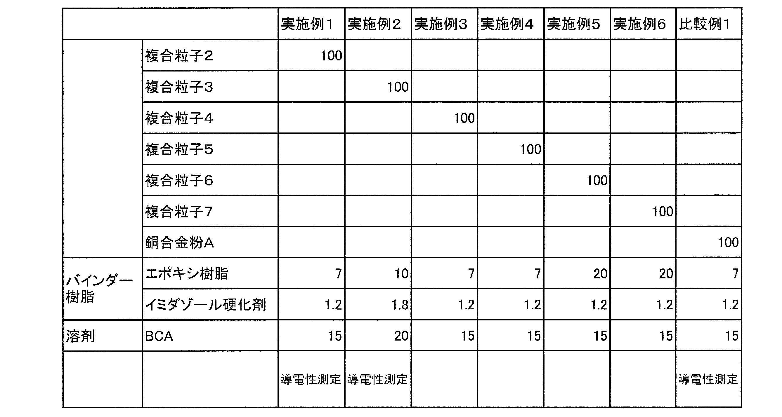

上記のようにして得られた各導電性ペーストについて導電性を評価した。
Claims (20)
- 周期表第8族~第10族に属する少なくとも1種の遷移金属を含む銅合金粉と、該銅合金粉の表面を覆っている炭素同素体とを含む、伝導性フィラー。
- 前記銅合金粉がフレーク状である、請求項1に記載の伝導性フィラー。
- 前記銅合金粉中の遷移金属の含有量が、前記銅合金粉100重量%に対し、0.3~6.0重量%である、請求項1又は2に記載の伝導性フィラー。
- 前記遷移金属が、鉄またはコバルトである、請求項1~3のいずれか1項に記載の伝導性フィラー。
- 前記遷移金属が、コバルトである、請求項4に記載の伝導性フィラー。
- 前記炭素同素体が銅合金粉の表面に、銅合金粉100重量%に対し、0重量%より大きく、3重量%以下の範囲で付着している、請求項1~5のいずれか1項に記載の伝導性フィラー。
- 前記炭素同素体がカーボンナノファイバーである、請求項1~6のいずれか1項に記載の伝導性フィラー。
- 請求項1~7のいずれか1項に記載の伝導性フィラーと、バインダー樹脂とを含む、伝導性ペースト。
- 前記バインダー樹脂が、エポキシ樹脂、ポリエステル樹脂、ウレタン樹脂、フェノール樹脂及びイミド樹脂からなる群から選択された少なくとも1種の樹脂である、請求項8に記載の伝導性ペースト。
- 前記伝導性フィラー100質量部に対し、前記バインダー樹脂を10~35質量部含む、請求項8又は9に記載の伝導性ペースト。
- 前記伝導性が電気伝導性である、請求項8~10のいずれか1項に記載の伝導性ペースト。
- 前記伝導性が熱伝導性である、請求項8~10のいずれか1項に記載の伝導性ペースト。
- 請求項1~7のいずれか1項に記載の伝導性フィラーの製造方法であって、
周期表第8族~第10族に属する少なくとも1種の遷移金属を含む銅合金粉を用意する工程と、
前記銅合金粉の表面に炭素源を接触させ伝導性フィラーを得る工程とを備える、伝導性フィラーの製造方法。 - 前記銅合金粉を用意する工程が、アトマイズ法により行われる、請求項13に記載の伝導性フィラーの製造方法。
- 前記銅合金粉の表面に炭素源を接触させ伝導性フィラーを得る工程が、
CVD処理、フレーク化処理、再CVD処理の順に処理することにより伝導性フィラーを得る工程である、請求項13又は14に記載の伝導性フィラーの製造方法。 - 前記銅合金粉の表面に炭素源を接触させ伝導性フィラーを得る工程が、
CVD処理、熱処理の順に処理することにより伝導性フィラーを得る工程である、請求項13又は14に記載の伝導性フィラーの製造方法。 - 前記熱処理が、不活性ガス雰囲気下において、750℃~1000℃の温度雰囲気下で行われる、請求項16に記載の伝導性フィラーの製造方法。
- 前記銅合金粉の表面に炭素源を接触させ伝導性フィラーを得る工程が、300℃~400℃で銅合金粉を炭素含有ガスに接触させる工程を含む、請求項13~17のいずれか1項に記載の伝導性フィラーの製造方法。
- 前記銅合金粉の表面に炭素源を接触させ伝導性フィラーを得る工程の前に、焼結阻害剤を添加し混合する工程をさらに備える、請求項13~18のいずれか1項に記載の伝導性フィラーの製造方法。
- 請求項13~19のいずれか1項に記載の伝導性フィラーの製造方法により、伝導性フィラーを製造する工程と、
前記伝導性フィラーと、バインダー樹脂とを混合した後、混練することにより伝導性ペーストを得る工程とを備える、伝導性ペーストの製造方法。
Priority Applications (5)
| Application Number | Priority Date | Filing Date | Title |
|---|---|---|---|
| KR1020167002305A KR102166230B1 (ko) | 2013-08-01 | 2014-07-29 | 전도성 필러 및 그의 제조 방법, 및 전도성 페이스트 및 그의 제조 방법 |
| CN201480043505.4A CN105556617B (zh) | 2013-08-01 | 2014-07-29 | 传导性填料及其制造方法、以及传导性糊剂及其制造方法 |
| US14/907,736 US10533098B2 (en) | 2013-08-01 | 2014-07-29 | Conductive filler, method for producing same, conductive paste and method for producing conductive paste |
| EP14832327.2A EP3029686B1 (en) | 2013-08-01 | 2014-07-29 | Conductive filler, method for producing same, conductive paste and method for producing conductive paste |
| JP2014538029A JP5756887B1 (ja) | 2013-08-01 | 2014-07-29 | 伝導性フィラー及びその製造方法、並びに伝導性ペースト及びその製造方法 |
Applications Claiming Priority (4)
| Application Number | Priority Date | Filing Date | Title |
|---|---|---|---|
| JP2013160480 | 2013-08-01 | ||
| JP2013-160480 | 2013-08-01 | ||
| JP2013-269465 | 2013-12-26 | ||
| JP2013269465 | 2013-12-26 |
Publications (1)
| Publication Number | Publication Date |
|---|---|
| WO2015016202A1 true WO2015016202A1 (ja) | 2015-02-05 |
Family
ID=52431735
Family Applications (1)
| Application Number | Title | Priority Date | Filing Date |
|---|---|---|---|
| PCT/JP2014/069901 WO2015016202A1 (ja) | 2013-08-01 | 2014-07-29 | 伝導性フィラー及びその製造方法、並びに伝導性ペースト及びその製造方法 |
Country Status (7)
| Country | Link |
|---|---|
| US (1) | US10533098B2 (ja) |
| EP (1) | EP3029686B1 (ja) |
| JP (1) | JP5756887B1 (ja) |
| KR (1) | KR102166230B1 (ja) |
| CN (1) | CN105556617B (ja) |
| TW (1) | TWI604021B (ja) |
| WO (1) | WO2015016202A1 (ja) |
Cited By (4)
| Publication number | Priority date | Publication date | Assignee | Title |
|---|---|---|---|---|
| JP2016151029A (ja) * | 2015-02-16 | 2016-08-22 | 積水化学工業株式会社 | 伝導性フィラー及びその製造方法並びに伝導性ペースト |
| JP2016195103A (ja) * | 2015-03-31 | 2016-11-17 | 東レ株式会社 | 複合導電性粒子およびその製造方法ならびに導電性樹脂 |
| JP2016207377A (ja) * | 2015-04-20 | 2016-12-08 | 積水化学工業株式会社 | 導電性ペースト |
| WO2019004331A1 (ja) * | 2017-06-30 | 2019-01-03 | 積水化学工業株式会社 | 導電性ペースト |
Families Citing this family (5)
| Publication number | Priority date | Publication date | Assignee | Title |
|---|---|---|---|---|
| JP6530709B2 (ja) * | 2014-03-05 | 2019-06-12 | 積水化学工業株式会社 | 伝導性フィラー、伝導性フィラーの製造方法及び伝導性ペースト |
| JP6908398B2 (ja) * | 2017-03-08 | 2021-07-28 | 株式会社Adeka | 樹脂組成物、硬化物を形成する方法および硬化物 |
| CN113098163B (zh) * | 2021-04-19 | 2023-03-24 | 云南铜业压铸科技有限公司 | 一种高转速电动机用铸铜转子的制备方法 |
| CN114101659B (zh) * | 2021-12-06 | 2024-04-19 | 赵玉荣 | 一种铜合金碳纳米管复合材料及其制备方法和应用 |
| CN114334221B (zh) * | 2022-01-10 | 2024-02-09 | 珠海方正科技多层电路板有限公司 | 一种塞孔铜浆及其制备方法、印刷线路板 |
Citations (13)
| Publication number | Priority date | Publication date | Assignee | Title |
|---|---|---|---|---|
| JPH07331125A (ja) * | 1994-06-08 | 1995-12-19 | Asahi Chem Ind Co Ltd | 導電性ペースト |
| JPH07331360A (ja) * | 1994-06-06 | 1995-12-19 | Asahi Chem Ind Co Ltd | 新規な銅合金粉末及びその製造方法 |
| JP2002008444A (ja) * | 2000-06-27 | 2002-01-11 | Hitachi Chem Co Ltd | 導電ペースト |
| JP2004169081A (ja) * | 2002-11-19 | 2004-06-17 | Mitsui Mining & Smelting Co Ltd | 金属粉及びその製造方法 |
| JP2008074647A (ja) | 2006-09-19 | 2008-04-03 | National Institute Of Advanced Industrial & Technology | カーボンナノチューブの製造方法 |
| JP2008285697A (ja) * | 2007-05-15 | 2008-11-27 | Ishihara Sangyo Kaisha Ltd | 金属微粒子及びその製造方法並びにそれを含有した流動性組成物 |
| WO2009054309A1 (ja) * | 2007-10-25 | 2009-04-30 | National University Corporation Hokkaido University | 複合金属材およびその製造方法 |
| JP2010053440A (ja) * | 2007-09-14 | 2010-03-11 | Jfe Steel Corp | 粉末冶金用鉄基粉末 |
| JP2011225993A (ja) * | 2010-04-14 | 2011-11-10 | Korea Advanced Inst Of Science & Technology | グラフェン/金属ナノ複合粉末及びその製造方法 |
| JP2013040403A (ja) * | 2011-08-16 | 2013-02-28 | Samsung Electro-Mechanics Co Ltd | 金属粉末、その製造方法、及びその金属粉末からなる内部電極を含む積層セラミックキャパシタ |
| JP2013513730A (ja) * | 2009-12-14 | 2013-04-22 | テクノロジアン テュトキムスケスクス ヴェーテーテー | 金属ナノ粒子を炭素で表面被覆する方法 |
| JP2013091824A (ja) * | 2011-10-25 | 2013-05-16 | Kri Inc | カーボン複合金属微粒子およびその製造方法 |
| JP2013091816A (ja) * | 2011-10-24 | 2013-05-16 | Katsuyoshi Kondo | 銅合金素材及びその製造方法 |
Family Cites Families (12)
| Publication number | Priority date | Publication date | Assignee | Title |
|---|---|---|---|---|
| JP2003268567A (ja) * | 2002-03-19 | 2003-09-25 | Hitachi Cable Ltd | 導電材被覆耐食性金属材料 |
| JP3999676B2 (ja) * | 2003-01-22 | 2007-10-31 | Dowaホールディングス株式会社 | 銅基合金およびその製造方法 |
| JP4421556B2 (ja) * | 2003-02-18 | 2010-02-24 | 国立大学法人信州大学 | 金属粒子およびその製造方法 |
| KR100570634B1 (ko) | 2003-10-16 | 2006-04-12 | 한국전자통신연구원 | 탄소나노튜브와 금속분말 혼성 복합에 의해 제조된 전자파차폐재 |
| US20070190348A1 (en) * | 2004-10-21 | 2007-08-16 | Kouichi Ichiki | Composite metal article and production method thereof |
| CN100499223C (zh) * | 2005-12-09 | 2009-06-10 | 中国科学院物理研究所 | 一种表面包覆碳的层状结构含锂复合金属氧化物及其应用 |
| JP5077660B2 (ja) | 2007-07-25 | 2012-11-21 | 三菱マテリアル株式会社 | 金属粉末複合材を製造するコーティング組成物と、該金属粉末複合材によって製造された金属複合材、金属積層複合材、およびこれらの製造方法 |
| DE102008035756A1 (de) * | 2008-07-31 | 2010-02-04 | Robert Bosch Gmbh | Vorrichtung und Verfahren zum Reduzieren des Energieverbrauchs einer Maschine oder Anlage |
| KR101065778B1 (ko) * | 2008-10-14 | 2011-09-20 | 한국과학기술연구원 | 탄소나노튜브 피복 실리콘-구리 복합 입자 및 그 제조 방법과, 이를 이용한 이차전지용 음극 및 이차전지 |
| KR101310094B1 (ko) * | 2010-10-26 | 2013-09-24 | 한국과학기술연구원 | 구리 입자를 포함하는 탄소나노섬유, 나노입자, 분산용액 및 그 제조방법 |
| US20160367971A1 (en) * | 2013-07-30 | 2016-12-22 | Northeastern University | Catalyst and Method for Synthesis of Carbon Nanomaterials |
| JP6530709B2 (ja) | 2014-03-05 | 2019-06-12 | 積水化学工業株式会社 | 伝導性フィラー、伝導性フィラーの製造方法及び伝導性ペースト |
-
2014
- 2014-07-29 JP JP2014538029A patent/JP5756887B1/ja active Active
- 2014-07-29 KR KR1020167002305A patent/KR102166230B1/ko active IP Right Grant
- 2014-07-29 WO PCT/JP2014/069901 patent/WO2015016202A1/ja active Application Filing
- 2014-07-29 CN CN201480043505.4A patent/CN105556617B/zh active Active
- 2014-07-29 EP EP14832327.2A patent/EP3029686B1/en active Active
- 2014-07-29 US US14/907,736 patent/US10533098B2/en not_active Expired - Fee Related
- 2014-08-01 TW TW103126493A patent/TWI604021B/zh not_active IP Right Cessation
Patent Citations (13)
| Publication number | Priority date | Publication date | Assignee | Title |
|---|---|---|---|---|
| JPH07331360A (ja) * | 1994-06-06 | 1995-12-19 | Asahi Chem Ind Co Ltd | 新規な銅合金粉末及びその製造方法 |
| JPH07331125A (ja) * | 1994-06-08 | 1995-12-19 | Asahi Chem Ind Co Ltd | 導電性ペースト |
| JP2002008444A (ja) * | 2000-06-27 | 2002-01-11 | Hitachi Chem Co Ltd | 導電ペースト |
| JP2004169081A (ja) * | 2002-11-19 | 2004-06-17 | Mitsui Mining & Smelting Co Ltd | 金属粉及びその製造方法 |
| JP2008074647A (ja) | 2006-09-19 | 2008-04-03 | National Institute Of Advanced Industrial & Technology | カーボンナノチューブの製造方法 |
| JP2008285697A (ja) * | 2007-05-15 | 2008-11-27 | Ishihara Sangyo Kaisha Ltd | 金属微粒子及びその製造方法並びにそれを含有した流動性組成物 |
| JP2010053440A (ja) * | 2007-09-14 | 2010-03-11 | Jfe Steel Corp | 粉末冶金用鉄基粉末 |
| WO2009054309A1 (ja) * | 2007-10-25 | 2009-04-30 | National University Corporation Hokkaido University | 複合金属材およびその製造方法 |
| JP2013513730A (ja) * | 2009-12-14 | 2013-04-22 | テクノロジアン テュトキムスケスクス ヴェーテーテー | 金属ナノ粒子を炭素で表面被覆する方法 |
| JP2011225993A (ja) * | 2010-04-14 | 2011-11-10 | Korea Advanced Inst Of Science & Technology | グラフェン/金属ナノ複合粉末及びその製造方法 |
| JP2013040403A (ja) * | 2011-08-16 | 2013-02-28 | Samsung Electro-Mechanics Co Ltd | 金属粉末、その製造方法、及びその金属粉末からなる内部電極を含む積層セラミックキャパシタ |
| JP2013091816A (ja) * | 2011-10-24 | 2013-05-16 | Katsuyoshi Kondo | 銅合金素材及びその製造方法 |
| JP2013091824A (ja) * | 2011-10-25 | 2013-05-16 | Kri Inc | カーボン複合金属微粒子およびその製造方法 |
Non-Patent Citations (1)
| Title |
|---|
| See also references of EP3029686A4 |
Cited By (5)
| Publication number | Priority date | Publication date | Assignee | Title |
|---|---|---|---|---|
| JP2016151029A (ja) * | 2015-02-16 | 2016-08-22 | 積水化学工業株式会社 | 伝導性フィラー及びその製造方法並びに伝導性ペースト |
| JP2016195103A (ja) * | 2015-03-31 | 2016-11-17 | 東レ株式会社 | 複合導電性粒子およびその製造方法ならびに導電性樹脂 |
| JP2016207377A (ja) * | 2015-04-20 | 2016-12-08 | 積水化学工業株式会社 | 導電性ペースト |
| WO2019004331A1 (ja) * | 2017-06-30 | 2019-01-03 | 積水化学工業株式会社 | 導電性ペースト |
| US10984921B2 (en) | 2017-06-30 | 2021-04-20 | Sekisui Chemical Co., Ltd. | Conductive paste |
Also Published As
| Publication number | Publication date |
|---|---|
| JP5756887B1 (ja) | 2015-07-29 |
| EP3029686A1 (en) | 2016-06-08 |
| KR20160037915A (ko) | 2016-04-06 |
| CN105556617A (zh) | 2016-05-04 |
| TWI604021B (zh) | 2017-11-01 |
| EP3029686A4 (en) | 2017-03-22 |
| TW201510110A (zh) | 2015-03-16 |
| US20160168395A1 (en) | 2016-06-16 |
| KR102166230B1 (ko) | 2020-10-15 |
| JPWO2015016202A1 (ja) | 2017-03-02 |
| CN105556617B (zh) | 2018-08-24 |
| EP3029686B1 (en) | 2020-09-02 |
| US10533098B2 (en) | 2020-01-14 |
Similar Documents
| Publication | Publication Date | Title |
|---|---|---|
| JP5756887B1 (ja) | 伝導性フィラー及びその製造方法、並びに伝導性ペースト及びその製造方法 | |
| Ren et al. | Current progress on the modification of carbon nanotubes and their application in electromagnetic wave absorption | |
| Wang et al. | Electromagnetic interference shielding MWCNT-Fe3O4@ Ag/epoxy nanocomposites with satisfactory thermal conductivity and high thermal stability | |
| Zhu et al. | Flexible Fe3O4/graphene foam/poly dimethylsiloxane composite for high-performance electromagnetic interference shielding | |
| WO2018228407A1 (zh) | 一种石墨烯/金属纳米带复合导电油墨及其制备方法和应用 | |
| Jin et al. | Facile physical route to highly crystalline graphene | |
| Meschi Amoli et al. | Highly electrically conductive adhesives using silver nanoparticle (Ag NP)-decorated graphene: The effect of NPs sintering on the electrical conductivity improvement | |
| EP3816103A1 (en) | Carbon nanotube dispersion and usage therefor | |
| TWI425893B (zh) | 銅配線圖案形成方法以及該方法所使用的氧化銅粒子分散液 | |
| Lee et al. | Stable high-capacity lithium ion battery anodes produced by supersonic spray deposition of hematite nanoparticles and self-healing reduced graphene oxide | |
| WO2012133627A1 (ja) | 銀コート銅粉及びその製造法、該銀コート銅粉を含有する導電性ペースト、導電性接着剤、導電性膜、及び電気回路 | |
| JP6530709B2 (ja) | 伝導性フィラー、伝導性フィラーの製造方法及び伝導性ペースト | |
| Bansala et al. | Synthesis and shielding properties of PVP-stabilized-AgNPs-based graphene nanohybrid in the Ku band | |
| Yi et al. | Effect of iron-deposited graphene oxides on the electromagnetic wave absorbing property of polymer composite films with Fe-based hollow magnetic fibers for near-field applications | |
| JP6457834B2 (ja) | 伝導性フィラー及びその製造方法並びに伝導性ペースト | |
| Yang et al. | One step synthesis of a hybrid Ag/rGO conductive ink using a complexation–covalent bonding based approach | |
| KR101843795B1 (ko) | 나노 박막 코팅의 제조방법 | |
| Shen et al. | Stretchable silver@ CNT-poly (vinyl alcohol) films with efficient electromagnetic shielding prepared by polydopamine functionalization | |
| KR101573241B1 (ko) | 3차원 그래핀 구조체 및 이를 이용한 전극 제조방법 | |
| Fang et al. | In situ construction of efficient electromagnetic function Graphene/PES composites based on liquid phase exfoliation strategy | |
| Aïssa et al. | Super-high-frequency shielding properties of excimer-laser-synthesized-single-wall-carbon-nanotubes/polyurethane nanocomposite films | |
| KR101540030B1 (ko) | Ag가 코팅된 그래핀나노플레이트 및 이의 제조방법 | |
| JP2016207377A (ja) | 導電性ペースト | |
| TW201905935A (zh) | 導電性糊 | |
| Liu et al. | A “popcorn-making-mimic” strategy for compounding graphene@ NiFe2O4 flexible films for exceptionally strong electromagnetic interference shielding and absorption |
Legal Events
| Date | Code | Title | Description |
|---|---|---|---|
| WWE | Wipo information: entry into national phase |
Ref document number: 201480043505.4 Country of ref document: CN |
|
| ENP | Entry into the national phase |
Ref document number: 2014538029 Country of ref document: JP Kind code of ref document: A |
|
| 121 | Ep: the epo has been informed by wipo that ep was designated in this application |
Ref document number: 14832327 Country of ref document: EP Kind code of ref document: A1 |
|
| WWE | Wipo information: entry into national phase |
Ref document number: 2014832327 Country of ref document: EP |
|
| WWE | Wipo information: entry into national phase |
Ref document number: 14907736 Country of ref document: US |
|
| ENP | Entry into the national phase |
Ref document number: 20167002305 Country of ref document: KR Kind code of ref document: A |
|
| NENP | Non-entry into the national phase |
Ref country code: DE |