WO2014162999A1 - 圧電体膜および圧電体膜の製造方法 - Google Patents
圧電体膜および圧電体膜の製造方法 Download PDFInfo
- Publication number
- WO2014162999A1 WO2014162999A1 PCT/JP2014/059124 JP2014059124W WO2014162999A1 WO 2014162999 A1 WO2014162999 A1 WO 2014162999A1 JP 2014059124 W JP2014059124 W JP 2014059124W WO 2014162999 A1 WO2014162999 A1 WO 2014162999A1
- Authority
- WO
- WIPO (PCT)
- Prior art keywords
- piezoelectric film
- piezoelectric
- film
- amount
- perovskite
- Prior art date
- Legal status (The legal status is an assumption and is not a legal conclusion. Google has not performed a legal analysis and makes no representation as to the accuracy of the status listed.)
- Ceased
Links
Images





Classifications
-
- B—PERFORMING OPERATIONS; TRANSPORTING
- B41—PRINTING; LINING MACHINES; TYPEWRITERS; STAMPS
- B41J—TYPEWRITERS; SELECTIVE PRINTING MECHANISMS, i.e. MECHANISMS PRINTING OTHERWISE THAN FROM A FORME; CORRECTION OF TYPOGRAPHICAL ERRORS
- B41J2/00—Typewriters or selective printing mechanisms characterised by the printing or marking process for which they are designed
- B41J2/005—Typewriters or selective printing mechanisms characterised by the printing or marking process for which they are designed characterised by bringing liquid or particles selectively into contact with a printing material
- B41J2/01—Ink jet
- B41J2/135—Nozzles
- B41J2/14—Structure thereof only for on-demand ink jet heads
- B41J2/14201—Structure of print heads with piezoelectric elements
- B41J2/14233—Structure of print heads with piezoelectric elements of film type, deformed by bending and disposed on a diaphragm
-
- C—CHEMISTRY; METALLURGY
- C04—CEMENTS; CONCRETE; ARTIFICIAL STONE; CERAMICS; REFRACTORIES
- C04B—LIME, MAGNESIA; SLAG; CEMENTS; COMPOSITIONS THEREOF, e.g. MORTARS, CONCRETE OR LIKE BUILDING MATERIALS; ARTIFICIAL STONE; CERAMICS; REFRACTORIES; TREATMENT OF NATURAL STONE
- C04B35/00—Shaped ceramic products characterised by their composition; Ceramics compositions; Processing powders of inorganic compounds preparatory to the manufacturing of ceramic products
- C04B35/01—Shaped ceramic products characterised by their composition; Ceramics compositions; Processing powders of inorganic compounds preparatory to the manufacturing of ceramic products based on oxide ceramics
- C04B35/48—Shaped ceramic products characterised by their composition; Ceramics compositions; Processing powders of inorganic compounds preparatory to the manufacturing of ceramic products based on oxide ceramics based on zirconium or hafnium oxides, zirconates, zircon or hafnates
- C04B35/49—Shaped ceramic products characterised by their composition; Ceramics compositions; Processing powders of inorganic compounds preparatory to the manufacturing of ceramic products based on oxide ceramics based on zirconium or hafnium oxides, zirconates, zircon or hafnates containing also titanium oxides or titanates
- C04B35/491—Shaped ceramic products characterised by their composition; Ceramics compositions; Processing powders of inorganic compounds preparatory to the manufacturing of ceramic products based on oxide ceramics based on zirconium or hafnium oxides, zirconates, zircon or hafnates containing also titanium oxides or titanates based on lead zirconates and lead titanates, e.g. PZT
- C04B35/493—Shaped ceramic products characterised by their composition; Ceramics compositions; Processing powders of inorganic compounds preparatory to the manufacturing of ceramic products based on oxide ceramics based on zirconium or hafnium oxides, zirconates, zircon or hafnates containing also titanium oxides or titanates based on lead zirconates and lead titanates, e.g. PZT containing also other lead compounds
-
- C—CHEMISTRY; METALLURGY
- C04—CEMENTS; CONCRETE; ARTIFICIAL STONE; CERAMICS; REFRACTORIES
- C04B—LIME, MAGNESIA; SLAG; CEMENTS; COMPOSITIONS THEREOF, e.g. MORTARS, CONCRETE OR LIKE BUILDING MATERIALS; ARTIFICIAL STONE; CERAMICS; REFRACTORIES; TREATMENT OF NATURAL STONE
- C04B35/00—Shaped ceramic products characterised by their composition; Ceramics compositions; Processing powders of inorganic compounds preparatory to the manufacturing of ceramic products
- C04B35/01—Shaped ceramic products characterised by their composition; Ceramics compositions; Processing powders of inorganic compounds preparatory to the manufacturing of ceramic products based on oxide ceramics
- C04B35/495—Shaped ceramic products characterised by their composition; Ceramics compositions; Processing powders of inorganic compounds preparatory to the manufacturing of ceramic products based on oxide ceramics based on vanadium, niobium, tantalum, molybdenum or tungsten oxides or solid solutions thereof with other oxides, e.g. vanadates, niobates, tantalates, molybdates or tungstates
- C04B35/497—Shaped ceramic products characterised by their composition; Ceramics compositions; Processing powders of inorganic compounds preparatory to the manufacturing of ceramic products based on oxide ceramics based on vanadium, niobium, tantalum, molybdenum or tungsten oxides or solid solutions thereof with other oxides, e.g. vanadates, niobates, tantalates, molybdates or tungstates based on solid solutions with lead oxides
- C04B35/499—Shaped ceramic products characterised by their composition; Ceramics compositions; Processing powders of inorganic compounds preparatory to the manufacturing of ceramic products based on oxide ceramics based on vanadium, niobium, tantalum, molybdenum or tungsten oxides or solid solutions thereof with other oxides, e.g. vanadates, niobates, tantalates, molybdates or tungstates based on solid solutions with lead oxides containing also titanates
-
- C—CHEMISTRY; METALLURGY
- C04—CEMENTS; CONCRETE; ARTIFICIAL STONE; CERAMICS; REFRACTORIES
- C04B—LIME, MAGNESIA; SLAG; CEMENTS; COMPOSITIONS THEREOF, e.g. MORTARS, CONCRETE OR LIKE BUILDING MATERIALS; ARTIFICIAL STONE; CERAMICS; REFRACTORIES; TREATMENT OF NATURAL STONE
- C04B35/00—Shaped ceramic products characterised by their composition; Ceramics compositions; Processing powders of inorganic compounds preparatory to the manufacturing of ceramic products
- C04B35/622—Forming processes; Processing powders of inorganic compounds preparatory to the manufacturing of ceramic products
- C04B35/62218—Forming processes; Processing powders of inorganic compounds preparatory to the manufacturing of ceramic products obtaining ceramic films, e.g. by using temporary supports
-
- C—CHEMISTRY; METALLURGY
- C23—COATING METALLIC MATERIAL; COATING MATERIAL WITH METALLIC MATERIAL; CHEMICAL SURFACE TREATMENT; DIFFUSION TREATMENT OF METALLIC MATERIAL; COATING BY VACUUM EVAPORATION, BY SPUTTERING, BY ION IMPLANTATION OR BY CHEMICAL VAPOUR DEPOSITION, IN GENERAL; INHIBITING CORROSION OF METALLIC MATERIAL OR INCRUSTATION IN GENERAL
- C23C—COATING METALLIC MATERIAL; COATING MATERIAL WITH METALLIC MATERIAL; SURFACE TREATMENT OF METALLIC MATERIAL BY DIFFUSION INTO THE SURFACE, BY CHEMICAL CONVERSION OR SUBSTITUTION; COATING BY VACUUM EVAPORATION, BY SPUTTERING, BY ION IMPLANTATION OR BY CHEMICAL VAPOUR DEPOSITION, IN GENERAL
- C23C14/00—Coating by vacuum evaporation, by sputtering or by ion implantation of the coating forming material
- C23C14/06—Coating by vacuum evaporation, by sputtering or by ion implantation of the coating forming material characterised by the coating material
- C23C14/08—Oxides
-
- C—CHEMISTRY; METALLURGY
- C23—COATING METALLIC MATERIAL; COATING MATERIAL WITH METALLIC MATERIAL; CHEMICAL SURFACE TREATMENT; DIFFUSION TREATMENT OF METALLIC MATERIAL; COATING BY VACUUM EVAPORATION, BY SPUTTERING, BY ION IMPLANTATION OR BY CHEMICAL VAPOUR DEPOSITION, IN GENERAL; INHIBITING CORROSION OF METALLIC MATERIAL OR INCRUSTATION IN GENERAL
- C23C—COATING METALLIC MATERIAL; COATING MATERIAL WITH METALLIC MATERIAL; SURFACE TREATMENT OF METALLIC MATERIAL BY DIFFUSION INTO THE SURFACE, BY CHEMICAL CONVERSION OR SUBSTITUTION; COATING BY VACUUM EVAPORATION, BY SPUTTERING, BY ION IMPLANTATION OR BY CHEMICAL VAPOUR DEPOSITION, IN GENERAL
- C23C14/00—Coating by vacuum evaporation, by sputtering or by ion implantation of the coating forming material
- C23C14/06—Coating by vacuum evaporation, by sputtering or by ion implantation of the coating forming material characterised by the coating material
- C23C14/08—Oxides
- C23C14/088—Oxides of the type ABO3 with A representing alkali, alkaline earth metal or Pb and B representing a refractory or rare earth metal
-
- C—CHEMISTRY; METALLURGY
- C23—COATING METALLIC MATERIAL; COATING MATERIAL WITH METALLIC MATERIAL; CHEMICAL SURFACE TREATMENT; DIFFUSION TREATMENT OF METALLIC MATERIAL; COATING BY VACUUM EVAPORATION, BY SPUTTERING, BY ION IMPLANTATION OR BY CHEMICAL VAPOUR DEPOSITION, IN GENERAL; INHIBITING CORROSION OF METALLIC MATERIAL OR INCRUSTATION IN GENERAL
- C23C—COATING METALLIC MATERIAL; COATING MATERIAL WITH METALLIC MATERIAL; SURFACE TREATMENT OF METALLIC MATERIAL BY DIFFUSION INTO THE SURFACE, BY CHEMICAL CONVERSION OR SUBSTITUTION; COATING BY VACUUM EVAPORATION, BY SPUTTERING, BY ION IMPLANTATION OR BY CHEMICAL VAPOUR DEPOSITION, IN GENERAL
- C23C14/00—Coating by vacuum evaporation, by sputtering or by ion implantation of the coating forming material
- C23C14/22—Coating by vacuum evaporation, by sputtering or by ion implantation of the coating forming material characterised by the process of coating
- C23C14/34—Sputtering
-
- C—CHEMISTRY; METALLURGY
- C23—COATING METALLIC MATERIAL; COATING MATERIAL WITH METALLIC MATERIAL; CHEMICAL SURFACE TREATMENT; DIFFUSION TREATMENT OF METALLIC MATERIAL; COATING BY VACUUM EVAPORATION, BY SPUTTERING, BY ION IMPLANTATION OR BY CHEMICAL VAPOUR DEPOSITION, IN GENERAL; INHIBITING CORROSION OF METALLIC MATERIAL OR INCRUSTATION IN GENERAL
- C23C—COATING METALLIC MATERIAL; COATING MATERIAL WITH METALLIC MATERIAL; SURFACE TREATMENT OF METALLIC MATERIAL BY DIFFUSION INTO THE SURFACE, BY CHEMICAL CONVERSION OR SUBSTITUTION; COATING BY VACUUM EVAPORATION, BY SPUTTERING, BY ION IMPLANTATION OR BY CHEMICAL VAPOUR DEPOSITION, IN GENERAL
- C23C14/00—Coating by vacuum evaporation, by sputtering or by ion implantation of the coating forming material
- C23C14/22—Coating by vacuum evaporation, by sputtering or by ion implantation of the coating forming material characterised by the process of coating
- C23C14/34—Sputtering
- C23C14/3407—Cathode assembly for sputtering apparatus, e.g. Target
- C23C14/3414—Metallurgical or chemical aspects of target preparation, e.g. casting, powder metallurgy
-
- C—CHEMISTRY; METALLURGY
- C23—COATING METALLIC MATERIAL; COATING MATERIAL WITH METALLIC MATERIAL; CHEMICAL SURFACE TREATMENT; DIFFUSION TREATMENT OF METALLIC MATERIAL; COATING BY VACUUM EVAPORATION, BY SPUTTERING, BY ION IMPLANTATION OR BY CHEMICAL VAPOUR DEPOSITION, IN GENERAL; INHIBITING CORROSION OF METALLIC MATERIAL OR INCRUSTATION IN GENERAL
- C23C—COATING METALLIC MATERIAL; COATING MATERIAL WITH METALLIC MATERIAL; SURFACE TREATMENT OF METALLIC MATERIAL BY DIFFUSION INTO THE SURFACE, BY CHEMICAL CONVERSION OR SUBSTITUTION; COATING BY VACUUM EVAPORATION, BY SPUTTERING, BY ION IMPLANTATION OR BY CHEMICAL VAPOUR DEPOSITION, IN GENERAL
- C23C14/00—Coating by vacuum evaporation, by sputtering or by ion implantation of the coating forming material
- C23C14/22—Coating by vacuum evaporation, by sputtering or by ion implantation of the coating forming material characterised by the process of coating
- C23C14/56—Apparatus specially adapted for continuous coating; Arrangements for maintaining the vacuum, e.g. vacuum locks
- C23C14/564—Means for minimising impurities in the coating chamber such as dust, moisture, residual gases
-
- H—ELECTRICITY
- H10—SEMICONDUCTOR DEVICES; ELECTRIC SOLID-STATE DEVICES NOT OTHERWISE PROVIDED FOR
- H10N—ELECTRIC SOLID-STATE DEVICES NOT OTHERWISE PROVIDED FOR
- H10N30/00—Piezoelectric or electrostrictive devices
- H10N30/01—Manufacture or treatment
- H10N30/07—Forming of piezoelectric or electrostrictive parts or bodies on an electrical element or another base
- H10N30/074—Forming of piezoelectric or electrostrictive parts or bodies on an electrical element or another base by depositing piezoelectric or electrostrictive layers, e.g. aerosol or screen printing
- H10N30/076—Forming of piezoelectric or electrostrictive parts or bodies on an electrical element or another base by depositing piezoelectric or electrostrictive layers, e.g. aerosol or screen printing by vapour phase deposition
-
- H—ELECTRICITY
- H10—SEMICONDUCTOR DEVICES; ELECTRIC SOLID-STATE DEVICES NOT OTHERWISE PROVIDED FOR
- H10N—ELECTRIC SOLID-STATE DEVICES NOT OTHERWISE PROVIDED FOR
- H10N30/00—Piezoelectric or electrostrictive devices
- H10N30/20—Piezoelectric or electrostrictive devices with electrical input and mechanical output, e.g. functioning as actuators or vibrators
- H10N30/204—Piezoelectric or electrostrictive devices with electrical input and mechanical output, e.g. functioning as actuators or vibrators using bending displacement, e.g. unimorph, bimorph or multimorph cantilever or membrane benders
- H10N30/2047—Membrane type
-
- H—ELECTRICITY
- H10—SEMICONDUCTOR DEVICES; ELECTRIC SOLID-STATE DEVICES NOT OTHERWISE PROVIDED FOR
- H10N—ELECTRIC SOLID-STATE DEVICES NOT OTHERWISE PROVIDED FOR
- H10N30/00—Piezoelectric or electrostrictive devices
- H10N30/80—Constructional details
- H10N30/85—Piezoelectric or electrostrictive active materials
- H10N30/853—Ceramic compositions
- H10N30/8548—Lead-based oxides
- H10N30/8554—Lead-zirconium titanate [PZT] based
-
- B—PERFORMING OPERATIONS; TRANSPORTING
- B41—PRINTING; LINING MACHINES; TYPEWRITERS; STAMPS
- B41J—TYPEWRITERS; SELECTIVE PRINTING MECHANISMS, i.e. MECHANISMS PRINTING OTHERWISE THAN FROM A FORME; CORRECTION OF TYPOGRAPHICAL ERRORS
- B41J2202/00—Embodiments of or processes related to ink-jet or thermal heads
- B41J2202/01—Embodiments of or processes related to ink-jet heads
- B41J2202/03—Specific materials used
-
- C—CHEMISTRY; METALLURGY
- C04—CEMENTS; CONCRETE; ARTIFICIAL STONE; CERAMICS; REFRACTORIES
- C04B—LIME, MAGNESIA; SLAG; CEMENTS; COMPOSITIONS THEREOF, e.g. MORTARS, CONCRETE OR LIKE BUILDING MATERIALS; ARTIFICIAL STONE; CERAMICS; REFRACTORIES; TREATMENT OF NATURAL STONE
- C04B2235/00—Aspects relating to ceramic starting mixtures or sintered ceramic products
- C04B2235/02—Composition of constituents of the starting material or of secondary phases of the final product
- C04B2235/30—Constituents and secondary phases not being of a fibrous nature
- C04B2235/32—Metal oxides, mixed metal oxides, or oxide-forming salts thereof, e.g. carbonates, nitrates, (oxy)hydroxides, chlorides
- C04B2235/3231—Refractory metal oxides, their mixed metal oxides, or oxide-forming salts thereof
- C04B2235/3232—Titanium oxides or titanates, e.g. rutile or anatase
-
- C—CHEMISTRY; METALLURGY
- C04—CEMENTS; CONCRETE; ARTIFICIAL STONE; CERAMICS; REFRACTORIES
- C04B—LIME, MAGNESIA; SLAG; CEMENTS; COMPOSITIONS THEREOF, e.g. MORTARS, CONCRETE OR LIKE BUILDING MATERIALS; ARTIFICIAL STONE; CERAMICS; REFRACTORIES; TREATMENT OF NATURAL STONE
- C04B2235/00—Aspects relating to ceramic starting mixtures or sintered ceramic products
- C04B2235/02—Composition of constituents of the starting material or of secondary phases of the final product
- C04B2235/30—Constituents and secondary phases not being of a fibrous nature
- C04B2235/32—Metal oxides, mixed metal oxides, or oxide-forming salts thereof, e.g. carbonates, nitrates, (oxy)hydroxides, chlorides
- C04B2235/3231—Refractory metal oxides, their mixed metal oxides, or oxide-forming salts thereof
- C04B2235/3244—Zirconium oxides, zirconates, hafnium oxides, hafnates, or oxide-forming salts thereof
-
- C—CHEMISTRY; METALLURGY
- C04—CEMENTS; CONCRETE; ARTIFICIAL STONE; CERAMICS; REFRACTORIES
- C04B—LIME, MAGNESIA; SLAG; CEMENTS; COMPOSITIONS THEREOF, e.g. MORTARS, CONCRETE OR LIKE BUILDING MATERIALS; ARTIFICIAL STONE; CERAMICS; REFRACTORIES; TREATMENT OF NATURAL STONE
- C04B2235/00—Aspects relating to ceramic starting mixtures or sintered ceramic products
- C04B2235/02—Composition of constituents of the starting material or of secondary phases of the final product
- C04B2235/30—Constituents and secondary phases not being of a fibrous nature
- C04B2235/32—Metal oxides, mixed metal oxides, or oxide-forming salts thereof, e.g. carbonates, nitrates, (oxy)hydroxides, chlorides
- C04B2235/3231—Refractory metal oxides, their mixed metal oxides, or oxide-forming salts thereof
- C04B2235/3251—Niobium oxides, niobates, tantalum oxides, tantalates, or oxide-forming salts thereof
-
- C—CHEMISTRY; METALLURGY
- C04—CEMENTS; CONCRETE; ARTIFICIAL STONE; CERAMICS; REFRACTORIES
- C04B—LIME, MAGNESIA; SLAG; CEMENTS; COMPOSITIONS THEREOF, e.g. MORTARS, CONCRETE OR LIKE BUILDING MATERIALS; ARTIFICIAL STONE; CERAMICS; REFRACTORIES; TREATMENT OF NATURAL STONE
- C04B2235/00—Aspects relating to ceramic starting mixtures or sintered ceramic products
- C04B2235/02—Composition of constituents of the starting material or of secondary phases of the final product
- C04B2235/30—Constituents and secondary phases not being of a fibrous nature
- C04B2235/32—Metal oxides, mixed metal oxides, or oxide-forming salts thereof, e.g. carbonates, nitrates, (oxy)hydroxides, chlorides
- C04B2235/3231—Refractory metal oxides, their mixed metal oxides, or oxide-forming salts thereof
- C04B2235/3251—Niobium oxides, niobates, tantalum oxides, tantalates, or oxide-forming salts thereof
- C04B2235/3255—Niobates or tantalates, e.g. silver niobate
-
- C—CHEMISTRY; METALLURGY
- C04—CEMENTS; CONCRETE; ARTIFICIAL STONE; CERAMICS; REFRACTORIES
- C04B—LIME, MAGNESIA; SLAG; CEMENTS; COMPOSITIONS THEREOF, e.g. MORTARS, CONCRETE OR LIKE BUILDING MATERIALS; ARTIFICIAL STONE; CERAMICS; REFRACTORIES; TREATMENT OF NATURAL STONE
- C04B2235/00—Aspects relating to ceramic starting mixtures or sintered ceramic products
- C04B2235/02—Composition of constituents of the starting material or of secondary phases of the final product
- C04B2235/30—Constituents and secondary phases not being of a fibrous nature
- C04B2235/42—Non metallic elements added as constituents or additives, e.g. sulfur, phosphor, selenium or tellurium
- C04B2235/422—Carbon
-
- C—CHEMISTRY; METALLURGY
- C04—CEMENTS; CONCRETE; ARTIFICIAL STONE; CERAMICS; REFRACTORIES
- C04B—LIME, MAGNESIA; SLAG; CEMENTS; COMPOSITIONS THEREOF, e.g. MORTARS, CONCRETE OR LIKE BUILDING MATERIALS; ARTIFICIAL STONE; CERAMICS; REFRACTORIES; TREATMENT OF NATURAL STONE
- C04B2235/00—Aspects relating to ceramic starting mixtures or sintered ceramic products
- C04B2235/70—Aspects relating to sintered or melt-casted ceramic products
- C04B2235/72—Products characterised by the absence or the low content of specific components, e.g. alkali metal free alumina ceramics
- C04B2235/721—Carbon content
-
- C—CHEMISTRY; METALLURGY
- C04—CEMENTS; CONCRETE; ARTIFICIAL STONE; CERAMICS; REFRACTORIES
- C04B—LIME, MAGNESIA; SLAG; CEMENTS; COMPOSITIONS THEREOF, e.g. MORTARS, CONCRETE OR LIKE BUILDING MATERIALS; ARTIFICIAL STONE; CERAMICS; REFRACTORIES; TREATMENT OF NATURAL STONE
- C04B2235/00—Aspects relating to ceramic starting mixtures or sintered ceramic products
- C04B2235/70—Aspects relating to sintered or melt-casted ceramic products
- C04B2235/74—Physical characteristics
- C04B2235/76—Crystal structural characteristics, e.g. symmetry
-
- C—CHEMISTRY; METALLURGY
- C04—CEMENTS; CONCRETE; ARTIFICIAL STONE; CERAMICS; REFRACTORIES
- C04B—LIME, MAGNESIA; SLAG; CEMENTS; COMPOSITIONS THEREOF, e.g. MORTARS, CONCRETE OR LIKE BUILDING MATERIALS; ARTIFICIAL STONE; CERAMICS; REFRACTORIES; TREATMENT OF NATURAL STONE
- C04B2235/00—Aspects relating to ceramic starting mixtures or sintered ceramic products
- C04B2235/70—Aspects relating to sintered or melt-casted ceramic products
- C04B2235/80—Phases present in the sintered or melt-cast ceramic products other than the main phase
Definitions
- the present invention relates to a piezoelectric film and a method for manufacturing the piezoelectric film, and more particularly to a piezoelectric film and a method for manufacturing the piezoelectric film with reduced supply current and power consumption.
- a piezoelectric element including a piezoelectric body having a piezoelectric property that expands and contracts as the electric field application intensity increases and decreases and an electrode that applies an electric field to the piezoelectric body is used for applications such as a piezoelectric actuator mounted on an ink jet recording head. in use.
- the piezoelectric material perovskite oxides such as lead zirconate titanate (PZT) are widely used.
- PZT lead zirconate titanate
- Such a piezoelectric material is a ferroelectric having spontaneous polarization when no electric field is applied.
- Patent Documents 1 and 2 describe PZT heavily doped with Nb.
- Nb By doping Nb at a high concentration, Patent Document 1 describes that oxygen deficiency can be reduced, leakage current can be reduced, and ferroelectric hysteresis characteristics are improved.
- Patent Document 2 describes that the piezoelectric characteristics are improved.
- Patent Document 3 by setting the carbon intensity ratio, which is the ratio of the maximum value and the minimum value of the carbon intensity of the piezoelectric film, to 8 or more and 28 or less, the relative dielectric constant can be increased and the piezoelectric constant is improved. It is described that it can be made.
- Patent Documents 1 and 2 describe that the piezoelectric constant is improved, but how the relative dielectric constant ( ⁇ ) and dielectric loss (tan ⁇ ) change, that is, the supply current to the piezoelectric film. It was not described how the power consumption changed and how it could be controlled.
- the piezoelectric constant d is expressed by the following formula (A), where k is an electromechanical coupling constant and Y is a Young's modulus (hardness) of the piezoelectric film.
- the present invention has been made in view of such circumstances, and suppresses the relative permittivity ⁇ and the dielectric loss tan ⁇ while maintaining the piezoelectric constant improved by doping with donor ions, that is, supply to the piezoelectric film.
- An object of the present invention is to provide a piezoelectric film and a method for manufacturing the piezoelectric film that can suppress current and power consumption.
- the present invention provides a piezoelectric film having a perovskite crystal structure represented by the following formula (P), which has a piezoelectric constant d 31 [pm / V], a relative dielectric constant ⁇ [ ⁇ ].
- the relative dielectric constant ⁇ is a physical quantity indicating how much the atoms in the material respond when an electric field is applied to the material.
- the dielectric loss tan ⁇ is a constant representing the degree of electrical energy loss that occurs when an AC electric field is applied to the piezoelectric body.
- the value obtained by (d 31 ) 2 / ( ⁇ ⁇ tan ⁇ ⁇ 1000) is a numerical value exceeding 3.
- a piezoelectric film having a high piezoelectric constant d 31 has a high relative dielectric constant ⁇ , but the relative dielectric constant ⁇ and the dielectric loss tan ⁇ are kept low, and the numerical value of the above equation is set to a value exceeding 3. supplying current to the piezoelectric film, it can reduce power consumption and to efficient piezoelectric film having a high piezoelectric constant d 31.
- the crystal constituting the perovskite crystal structure is mainly composed of a crystal having a plane orientation of (100) or (001).
- the piezoelectric constant d 31 can be improved.
- (D 31 ) 2 / ( ⁇ ⁇ tan ⁇ ⁇ 1000) can be increased and driven at a low voltage.
- the thickness of the piezoelectric film is preferably 2 ⁇ m or more and 10 ⁇ m or less.
- the piezoelectric film according to another aspect of the present invention an efficient piezoelectric film can be obtained even when the thickness of the piezoelectric film is in the above range.
- y in the formula (P) is preferably in the range of y ⁇ 0.18.
- the piezoelectric constant d 31 is improved, but the relative permittivity ⁇ and dielectric loss tan ⁇ of the piezoelectric film are increased. According to the piezoelectric film according to another aspect of the present invention, an efficient piezoelectric film can be obtained even when the doping amount (y) of Nb is 18% or more.
- the crystals constituting the perovskite crystal structure are preferably columnar crystals.
- the crystal structure constituting the piezoelectric film is a columnar crystal
- an alignment film having a uniform crystal orientation can be obtained, and high piezoelectric performance can be obtained. it can.
- the present invention provides a piezoelectric film having a perovskite crystal structure represented by the following formula (P), wherein the thickness of the piezoelectric film is 2 ⁇ m or more, and the piezoelectric film There is provided a piezoelectric film containing carbon on the surface of which the number of precipitated particles having a particle size of 200 nm or more is 1000 or less per 1 ⁇ m 2 .
- a piezoelectric film that easily captures carbon with a Nb doping amount (y) of 14% or more and a piezoelectric film thickness of 2 ⁇ m or more as an index of the carbon amount in the piezoelectric film
- the number of precipitated particles containing carbon and having a particle size of 200 nm or more is set to 1000 / ⁇ m 2 or less.
- the thickness of the piezoelectric film is preferably 3 ⁇ m or more.
- the piezoelectric film according to another aspect of the present invention is effective for a piezoelectric film that has a film thickness of 3 ⁇ m or more and that easily contains carbon.
- the present invention provides a method for manufacturing a piezoelectric film having a perovskite crystal structure represented by the following formula (P), and has a composition corresponding to the film composition of the piezoelectric film to be formed.
- a method for manufacturing a piezoelectric film in which a film is formed by sputtering using a raw material target having a carbon concentration of 200 ppm or less.
- the piezoelectric constant can be improved by doping the piezoelectric film with more than 14% of Nb. Furthermore, by reducing the carbon, it is possible to reduce the relative dielectric constant ⁇ and tan ⁇ while maintaining the piezoelectric constant, so that an efficient piezoelectric film with reduced supply power and power consumption can be obtained.
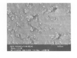
- FIG. 1A is a secondary electron image of the piezoelectric film after film formation.
- FIG. 1B is a reflected electron image of the piezoelectric film after film formation.
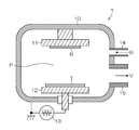
- FIG. 2 is a schematic sectional view of the sputtering apparatus.
- FIG. 3 is an explanatory diagram showing a method for measuring the plasma potential Vs and the floating potential Vf.
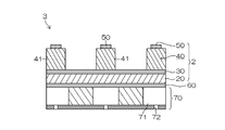
- FIG. 4 is a cross-sectional view showing the structure of the piezoelectric element and the ink jet recording apparatus.
- FIG. 5 is an overall configuration diagram showing an outline of the ink jet recording apparatus.
- FIG. 6 is a diagram illustrating an XRD (X-ray diffraction) pattern according to the first embodiment.
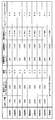
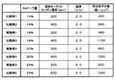
- FIG. 7 is a table showing the results of Test Example 1.
- FIG. 8 is a table showing the results of Test Example 2.
- FIG. 9 is a table showing the results of Test Example 2.
- the piezoelectric film of the present invention is a piezoelectric film having a perovskite crystal structure represented by the following general formula (P) as a main component.
- PZT-based perovskite oxide exhibits high piezoelectric performance at and near the morphotropic phase boundary (MPB).
- MPB morphotropic phase boundary
- a rhombohedral system is formed when Zr is rich, and a tetragonal system is formed when Ti is rich. It has become. Therefore, a in the general formula (P) is preferably MPB composition or close thereto. Specifically, it is preferable that 0.45 ⁇ a ⁇ 0.55.
- the amount of Nb is y> 0.14, and preferably y ⁇ 0.18.
- the amount of Nb is y> 0.14, and preferably y ⁇ 0.18.
- the upper limit of the Nb amount is preferably y ⁇ 0.23.
- the power consumption in the piezoelectric film is proportional to ⁇ ⁇ tan ⁇ ⁇ V 2 where the applied voltage [V] is V, the relative dielectric constant [ ⁇ ] is ⁇ , and the dielectric loss [ ⁇ ] is tan ⁇ .
- the applied voltage is inversely proportional to the piezoelectric constant d 31 [pm / V]
- ( ⁇ ⁇ tan ⁇ ) / (d 31 ) 2 is an index of power consumption. That is, the higher the numerical value of the following formula (B), the more efficient the piezoelectric film.
- the denominator 1000 is used to simplify the numerical value.
- An efficient piezoelectric film in which the above formula (B) exceeds 3 is a piezoelectric film doped with Nb exceeding 14%, and the piezoelectric constant d 31 is improved and the relative permittivity ⁇ and dielectric loss tan ⁇ are increased. It was too expensive to get. Therefore, even if the power supply voltage can be lowered with a high piezoelectric constant, heat generation cannot be suppressed.
- the number of precipitated particles having a particle diameter of 200 nm or more including carbon on the surface of the piezoelectric film is 1000 / ⁇ m 2. The following can be obtained.
- the piezoelectric film is formed by sputtering
- carbonate or acetate is generally used as a raw material for the sintering target, or a carbon container is generally used as the sintering container. Even if it is not added, a certain amount of carbon is present in the piezoelectric film.
- MO-CVD Metal Organic Chemical Vapor Deposition
- sol-gel method a raw material containing carbon such as a complex or an alkoxide is used, and the carbon inclusion is unavoidable.
- Nb is doped to exceed 14%, and when the amount of Nb doped is increased, especially exceeding 14%, precipitated particles having a particle size of 200 nm or more containing carbon are extremely increased.
- Nb fills the ZrO 2 ⁇ TiO 2 site with Nb 2 O 5 .
- the doping amount of Nb is 14% or less, since the amount of Nb is not large, oxygen is released, and the released oxygen is combined with carbon and released as CO 2 . For this reason, carbon remaining in the piezoelectric film can be prevented.
- the supply of oxygen becomes excessive, oxygen is easily taken into the film, and oxygen is hardly released.
- the amount of carbon in the piezoelectric film can be controlled by the amount of carbon in the target used at the time of manufacture. However, in a film having an Nb doping amount of 14% or less, even if the amount of carbon in the film formation target is large. The amount of carbon in the piezoelectric film is small, and there is no need to control the amount of carbon.
- the piezoelectric constant can be improved by increasing the doping amount of Nb in the piezoelectric film, but the relative permittivity ⁇ and the dielectric loss tan ⁇ also increase, so that the supply current and the power consumption also increase.
- carbon contained in the raw material target of the piezoelectric film is likely to remain in the piezoelectric film.
- the carbon concentration of the raw material target is reduced by the manufacturing method described later, and the number of precipitated particles having a particle size of 200 nm or more containing carbon on the surface of the piezoelectric film is set to 1000 particles / ⁇ m 2 or less.
- the dielectric constant ⁇ and the dielectric loss tan ⁇ can be lowered while maintaining the piezoelectric constant, so that the supply current and the power consumption can be reduced.
- Precipitated particles having a particle size of 200 nm or more containing carbon are black granular particles having a particle size of 200 nm or more as observed with a normal optical microscope. For example, a photograph of a field of view of about 300 ⁇ m ⁇ 500 ⁇ m in the field of view of the optical microscope. And measure the number of visual recognition.
- This particle has a Nb content of more than 14%, unlike a “particle” that is conventionally known in a vacuum film forming apparatus and deposits during film formation due to a film deposition such as an apparatus wall being peeled off. These particles appear characteristically in the PZT thin film having a large piezoelectric constant, and also appear when the film forming chamber is cleaned.
- the crystal structure constituting the piezoelectric film is mainly composed of crystals having a plane orientation of (100) direction or (001) direction.
- a high piezoelectric constant can be obtained by using a piezoelectric film having a crystal structure whose main component is a crystal having a plane orientation of (100) or (001).
- the peak in the (100) direction may be the peak in the (001) direction.
- the film thickness of the piezoelectric film is preferably 2 ⁇ m or more.
- the film thickness is not clear, but it is thought to be as follows.
- the carbon taken into the piezoelectric film is released as CO 2 from the piezoelectric film by the mechanism described above. Even in a piezoelectric film in which the doping amount of Nb exceeds 14%, the amount of Nb doping is less than that of a film in which the doping amount of Nb is 14% or less. It seems that there is little remaining.
- the film thickness of the piezoelectric film is more preferably 3 ⁇ m or more.
- Thickening the film thickness is effective from the viewpoint of reducing the driving voltage of the piezoelectric thin film device.
- a piezoelectric film having a thickness of 2 ⁇ m or more is required together with a piezoelectric film having a thickness of less than 2 ⁇ m.
- a film having a thickness of 10 ⁇ m or less is preferable because the piezoelectric film itself can be displaced without being constrained.
- the piezoelectric film is preferably formed into a columnar crystal by vapor phase growth as described below. By forming it by vapor phase growth, the surface of the piezoelectric film can be smoothed. In addition, a thin piezoelectric film can be formed.
- the piezoelectric film having the perovskite crystal structure represented by the above formula (P) as a main component can be formed by a non-thermal equilibrium process.
- suitable film formation methods for the piezoelectric film of the present invention include sputtering, plasma CVD (Chemical Vapor Deposition), firing quench quench, annealing quench, and spray quench. Among these, the sputtering method is particularly preferable.
- the donor ions can be doped at a high concentration.
- the film in the non-thermal equilibrium process, can be formed at a relatively low film formation temperature that is lower than the temperature at which Si and Pb react with each other. preferable.
- factors that affect the characteristics of the film to be formed include the film formation temperature, the type of substrate, the composition of the substrate, the surface energy of the substrate, and the film formation pressure if there is a film previously formed on the substrate.
- the oxygen amount in the atmospheric gas, the input power, the substrate-target distance, the electron temperature and electron density in the plasma, the active species density in the plasma and the lifetime of the active species can be considered.
- Vs is the plasma potential in the plasma during film formation
- Vf is the floating potential
- Vs is the substrate-target distance D
- a simple film can be formed. That is, when the film temperature is plotted with the film formation temperature Ts as the horizontal axis and any of Vs ⁇ Vf, Vs and the substrate-target distance D as the vertical axis, a good quality film can be formed within a certain range. .
- FIG. 2 is a schematic sectional view of the entire apparatus.
- the sputtering apparatus 1 generates a plasma with a substrate holder 11 such as an electrostatic chuck that can hold the deposition substrate B and heat the deposition substrate B to a predetermined temperature.
- the vacuum vessel 10 generally includes a plasma electrode (cathode electrode) 12.
- the substrate holder 11 and the plasma electrode 12 are spaced apart from each other so that the target T is mounted on the plasma electrode 12.
- the plasma electrode 12 is connected to an RF power source 13.
- a gas introduction pipe 14 for introducing a gas G required for film formation into the vacuum container 10 and a gas discharge pipe 15 for exhausting the gas V in the vacuum container 10 are attached to the vacuum container 10.
- a gas G Ar, Ar / O 2 mixed gas, or the like is used.
- Vs which is the difference between the film formation temperature Ts (° C.) and the plasma potential Vs (V) in the plasma during film formation and the floating potential Vf (V). It is preferable that film formation is performed under the film formation conditions satisfying the following formulas (1) and (2), and film formation is performed under the film formation conditions satisfying the following formulas (1) to (3). It is particularly preferable to carry out.
- the potential of the plasma space P becomes the plasma potential Vs (V).
- the film formation substrate B is an insulator and is electrically insulated from the ground. Therefore, the film formation substrate B is in a floating state, and the potential thereof is a floating potential Vf (V).
- Vf floating potential
- the constituent elements of the target between the target T and the film formation substrate B have a kinetic energy corresponding to an acceleration voltage of a potential difference Vs ⁇ Vf between the potential of the plasma space P and the potential of the film formation substrate B. It is thought that it collides with the film-forming substrate B.
- Plasma potential Vs and floating potential Vf can be measured using a Langmuir probe.
- the tip of a Langmuir probe is inserted into the plasma space P and the voltage applied to the probe is changed, for example, current-voltage characteristics as shown in FIG. 3 can be obtained (Mitsuharu Onuma, “Plasma and Film Formation Fundamentals” p. .90, published by Nikkan Kogyo Shimbun).
- the probe potential at which the current becomes 0 is the floating potential Vf. This state is that the ion current and the electron current flow into the probe surface become equal.
- the surface of the metal in the insulating state and the surface of the substrate are at this potential.
- Vs ⁇ Vf can be changed by installing a ground between the substrate and the target.
- Pb loss depends not only on the film forming temperature but also on Vs ⁇ Vf.
- Pb, Zr, and Ti which are constituent elements of PZT, Pb has the largest sputtering rate and is easily sputtered.
- a piezoelectric film having a high piezoelectric constant can be obtained by determining film forming conditions within a range satisfying the above formulas (1) to (3).
- the number of precipitated particles having a particle diameter of 200 nm or more including carbon precipitated on the surface of the piezoelectric film is 1000 particles / ⁇ m 2 or less.
- the carbon concentration can be measured by a high-frequency combustion infrared absorption method, for example, a high-frequency combustion infrared absorption device CS-444 manufactured by LECO Japan GK.
- the carbon concentration in the raw material target that is usually used in the production of the conventional piezoelectric film was measured, it was about 600 ppm.
- Such a raw material target with a reduced carbon concentration can be produced as follows.
- the raw material target in the sputtering method is generally obtained by calcining the pulverized raw material powder at a lower temperature, then crushing it again and pressing the powder to pressurize it, and firing it at a temperature higher than the calcination temperature. To manufacture.
- a sintered body for example, 600 ppm
- a large amount of carbon remains is obtained.
- the carbon concentration in the target can be lowered.
- the carbon concentration is reduced by heating for a long time before densification of the bulk body at a temperature lower than the main firing temperature of pellet sintering, and then raising the firing temperature.
- a target with a small amount can be manufactured.
- the carbon concentration can be lowered by irradiating oxygen plasma in advance and applying UV light such as a low-pressure mercury lamp or excimer light. Also effective is a UV ozone method in which ozone is generated by irradiating UV light under oxygen and exposed to ozone while irradiating UV.
- FIG. 4 is a cross-sectional view of the main part of the ink jet recording head. In order to facilitate visual recognition, the scale of the constituent elements is appropriately changed from the actual one.
- the piezoelectric element 2 is an element in which a lower electrode 30, a piezoelectric film 40, and an upper electrode 50 are sequentially stacked on a substrate 20, and the thickness of the piezoelectric film 40 is reduced by the lower electrode 30 and the upper electrode 50. An electric field is applied in the direction.
- the piezoelectric film 40 is a piezoelectric film of the present invention containing a perovskite oxide represented by the above formula (P).
- the lower electrode 30 is formed on substantially the entire surface of the substrate 20, and a piezoelectric film 40 having a pattern in which line-shaped convex portions 41 extending from the front side to the rear side in the drawing are arranged in a stripe shape is formed thereon.
- An upper electrode 50 is formed on the portion 41.
- the pattern of the piezoelectric film 40 is not limited to that shown in the figure, and is appropriately designed.
- the piezoelectric film 40 may be a continuous film.
- the piezoelectric film 40 is not a continuous film, but is formed by a pattern composed of a plurality of projections 41 separated from each other, so that the individual projections 41 can be expanded and contracted smoothly and a larger displacement amount can be obtained. ,preferable.
- the substrate 20 is not particularly limited, and examples thereof include silicon, glass, stainless steel (SUS (Steel Use Stainless)), yttrium stabilized zirconia (YSZ), alumina, sapphire, silicon carbide, and the like.
- a laminated substrate such as an SOI (Silicon on Insulator) substrate in which a SiO 2 oxide film is formed on the surface of a silicon substrate may be used.
- the main component of the lower electrode 30 is not particularly limited, and examples thereof include metals or metal oxides such as Au, Pt, Ir, IrO 2 , RuO 2 , LaNiO 3 , and SrRuO 3 , and combinations thereof.
- the main component of the upper electrode 50 is not particularly limited, and examples include materials exemplified for the lower electrode 30, electrode materials generally used in semiconductor processes such as Al, Ta, Cr, and Cu, and combinations thereof. .
- the thickness of the lower electrode 30 and the upper electrode 50 is not particularly limited, and is, for example, about 200 nm.
- the ink jet recording head (liquid ejecting apparatus) 3 generally includes an ink chamber (liquid storing chamber) 71 in which ink is stored and an ink chamber on the lower surface of the substrate 20 of the piezoelectric element 2 having the above-described configuration via a vibration plate 60.
- a plurality of ink chambers 71 are provided corresponding to the number and pattern of the convex portions 41 of the piezoelectric film 40.
- the electric field strength applied to the convex portion 41 of the piezoelectric element 2 is increased / decreased for each convex portion 41 to expand / contract, thereby controlling the ejection of ink from the ink chamber 71 and the ejection amount. Is called.
- a part of the substrate 20 may be processed into the diaphragm 60 and the ink nozzle 70.
- the substrate 20 is made of a laminated substrate such as an SOI substrate
- the substrate 20 is etched from the back side to form the ink chamber 71, and the vibration plate 60 and the ink nozzle 70 are formed by processing the substrate itself. Can do.
- the piezoelectric element 2 and the ink jet recording head 3 of the present embodiment are configured as described above.
- FIG. 5 is an overall view of the apparatus.
- the ink jet recording apparatus 100 includes a plurality of ink jet recording heads 172M, 172K, 172C, and 172Y on a recording medium 124 (sometimes referred to as “paper” for convenience) held on an impression cylinder (drawing drum 170) of the drawing unit 116.
- a recording medium 124 sometimes referred to as “paper” for convenience
- This is an on-demand type image forming apparatus to which a two-liquid reaction (aggregation) method in which a processing liquid and an ink liquid are reacted to form an image on a recording medium 124 is applied.
- the ink jet recording apparatus 100 mainly includes a paper feeding unit 112, a treatment liquid application unit 114, a drawing unit 116, a drying unit 118, a fixing unit 120, and a discharge unit 122.
- the paper feeding unit 112 is a mechanism that supplies the recording medium 124 to the processing liquid application unit 114, and the recording medium 124 that is a sheet is stacked on the paper feeding unit 112.
- the paper feed unit 112 is provided with a paper feed tray 150, and the recording medium 124 is fed from the paper feed tray 150 to the processing liquid application unit 114 one by one.
- the processing liquid application unit 114 is a mechanism that applies the processing liquid to the recording surface of the recording medium 124.
- the treatment liquid contains a color material aggregating agent that agglomerates the color material (pigment in this example) in the ink applied by the drawing unit 116, and the ink comes into contact with the treatment liquid and the ink. And the solvent are promoted.
- the recording medium 124 to which the processing liquid is applied by the processing liquid application unit 114 is transferred from the processing liquid drum 154 to the drawing drum 170 of the drawing unit 116 via the intermediate transport unit 126.
- the drawing unit 116 includes a drawing drum (second transport body) 170, a sheet pressing roller 174, and ink jet recording heads 172M, 172K, 172C, and 172Y.
- the inkjet recording heads 172M, 172K, 172C, and 172Y are preferably full-line inkjet recording heads (inkjet heads) each having a length corresponding to the maximum width of the image forming area in the recording medium 124.
- a nozzle row in which a plurality of nozzles for ink ejection are arranged over the entire width of the image forming area is formed.
- Each of the ink jet recording heads 172M, 172K, 172C, and 172Y is installed so as to extend in a direction orthogonal to the conveyance direction of the recording medium 124 (the rotation direction of the drawing drum 170).
- a treatment liquid application unit is formed by ejecting droplets of the corresponding color ink from each of the ink jet recording heads 172M, 172K, 172C, and 172Y toward the recording surface of the recording medium 124 held in close contact with the drawing drum 170.
- the ink comes into contact with the processing liquid previously applied to the recording surface, and the color material (pigment) dispersed in the ink is aggregated to form a color material aggregate. Thereby, the color material flow on the recording medium 124 is prevented, and an image is formed on the recording surface of the recording medium 124.
- the recording medium 124 on which an image is formed by the drawing unit 116 is transferred from the drawing drum 170 to the drying drum 176 of the drying unit 118 via the intermediate conveyance unit 128.
- the drying unit 118 is a mechanism for drying moisture contained in the solvent separated by the color material aggregating action, and includes a drying drum (conveying body) 176 and a solvent drying device 178 as shown in FIG.
- the solvent drying device 178 is disposed at a position facing the outer peripheral surface of the drying drum 176, and includes an IR heater 182 and a hot air jet nozzle 180 disposed between the IR heaters 182.
- the recording medium 124 that has been dried by the drying unit 118 is transferred from the drying drum 176 to the fixing drum 184 of the fixing unit 120 via the intermediate conveyance unit 130.
- the fixing unit 120 includes a fixing drum 184, a halogen heater 186, a fixing roller 188, and an inline sensor 190. With the rotation of the fixing drum 184, the recording medium 124 is conveyed with the recording surface facing outward. The recording surface is preheated by the halogen heater 186, fixing processing by the fixing roller 188, and by the inline sensor 190. Inspection is performed.
- the fixing roller 188 is a roller member that heats and pressurizes the dried ink to weld the self-dispersing thermoplastic resin fine particles in the ink to form a film of the ink, and heats and pressurizes the recording medium 124. Composed.
- thermoplastic resin fine particles in the thin image layer formed by the drying unit 118 are heated and pressurized by the fixing roller 188 and are melted. Can be fixed and fixed.
- the image is irradiated with UV at the fixing unit equipped with a UV irradiation lamp.
- the monomer can be cured and polymerized to improve the image strength.
- the discharge unit 122 includes a discharge tray 192, and a transfer drum 194, a conveyance belt 196, and a stretching roller 198 are provided between the discharge tray 192 and the fixing drum 184 of the fixing unit 120 so as to be in contact therewith. It has been.
- the recording medium 124 is sent to the conveyor belt 196 by the transfer drum 194 and discharged to the discharge tray 192.
- drum conveyance type inkjet recording apparatus has been described with reference to FIG. 5, the present invention is not limited to this, and the invention can also be used in a belt conveyance type inkjet recording apparatus.
- Example 1 A Si film having a thickness of 20 nm and a (111) Ir film having a thickness of 150 nm were sequentially formed on the Si wafer as a lower electrode by sputtering. An Nb-PZT piezoelectric film was formed on the lower electrode. The total thickness of the Nb-PZT piezoelectric film was 2 ⁇ m.
- the conditions for forming the piezoelectric film were as follows. Film forming apparatus: RF sputtering apparatus ("ferroelectric film forming sputtering apparatus MPS type" manufactured by ULVAC), Target: 120 mm ⁇ Pb 1.3 ((Zr 0.52 Ti 0.48 ) 1-x Nb x ) O 3 sintered body (where x varies depending on the amount of Nb to be doped.
- RF sputtering apparatus (“ferroelectric film forming sputtering apparatus MPS type” manufactured by ULVAC)
- Target 120 mm ⁇ Pb 1.3 ((Zr 0.52 Ti 0.48 ) 1-x Nb x ) O 3 sintered body (where x varies depending on the amount of Nb to be doped.
- Deposition power 500W
- Deposition pressure 0.3 Pa
- Deposition gas: Ar / O 2 97.5 / 2.5 (molar ratio).
- the obtained piezoelectric film was subjected to XRD (X-ray diffraction) analysis by a ⁇ / 2 ⁇ measurement method using “X-ray diffraction apparatus ULTIMA for thin film evaluation” manufactured by Rigaku Corporation.
- XRD X-ray diffraction
- the peak of the pyrochlore phase was not observed, and the obtained piezoelectric film was a film having a perovskite single phase structure and good crystallinity.
- ⁇ I (Pyrochlore) / ( ⁇ I (Perovskite) + ⁇ I (Pyrochlore)) was calculated as the amount of pyrochlore (%).
- ⁇ I (pyrochlore) is the total reflection intensity from the pyrochlore phase
- ⁇ I (perovskite) is the total reflection intensity from the perovskite phase.
- the amount of pyrochlore was 0%.
- Ti 20 nm thickness / Pt: 150 nm thickness
- Pt mainly functions as an electrode
- relative permittivity ⁇ and dielectric loss tan ⁇ were measured with an impedance analyzer Agilent 4294A.
- the piezoelectric displacement was measured by processing the substrate into a diaphragm structure, applying a voltage, and applying a voltage of ⁇ 10 ⁇ 10 V with a laser Doppler vibrometer.
- the piezoelectric displacement d 31 was calculated by matching the piezoelectric displacement with the simulation using the ANSYS calculation.
- Example 2 and 3 Comparative Examples 1 to 5, Reference Example
- the doping amount of Nb is 14% (Comparative Examples 1 and 2), 20% (Example 2 and Comparative Example 4), 23% (Example 3 and Comparative Example 5), and the carbon content of the raw material target during film formation is 200 ppm.
- a film was formed in the same manner as in Example 1 except that (Comparative Example 1, Examples 2 and 3) and 600 ppm of the conventional raw material (Comparative Examples 2, 3, 4, and 5) were used.
- data on C92H manufactured by Fuji Ceramic which is known as a conventional high-performance piezoelectric bulk body, is also described.
- the piezoelectric constant was maintained as the value of the piezoelectric film formed with the conventional raw material target (carbon concentration of 600 ppm).
- the dielectric constant ⁇ and dielectric loss tan ⁇ could be lowered, and a good film with reduced supply current and power consumption could be obtained.
- the bulk ceramic when compared with a conventional bulk ceramic, can obtain a material having a higher piezoelectric constant than a thin film formed by sputtering.
- the relative dielectric constant ⁇ and the dielectric loss tan ⁇ are also increasing, and the numerical value of the following formula (B) is as low as 0.7, so that a high-quality material cannot be obtained.
- the increase in the relative permittivity ⁇ and the dielectric loss tan ⁇ in the bulk ceramics is not the same because the material composition is different, but in the embodiment of the present invention, the relative permittivity ⁇ and the dielectric loss tan ⁇ are low, the supply current, the consumption A piezoelectric film with reduced power was formed.
- Test Example 2 >> Next, for the piezoelectric films of Examples 1 to 3 and Comparative Examples 1 to 5 formed in Test Example 1, the number of precipitated particles having a particle diameter of 200 nm or more on the surface of the piezoelectric film was examined. The number of precipitated particles was confirmed by counting the number of precipitated particles per unit area from an electron micrograph. The results are shown in FIG. In the present invention, it can be confirmed that the relative dielectric constant ⁇ and the dielectric loss tan ⁇ can be suppressed when the number of precipitated particles is 1000 particles / ⁇ m 2 or less.
- the Nb doping amount is fixed at 23%
- the film thickness of the piezoelectric film is 3 ⁇ m (Example 4, Comparative Example 6), 4 ⁇ m (Example 5, Comparative Example 7)
- the carbon amount of the raw material target is changed.
- the number of precipitated particles was confirmed.
- the number of precipitated particles is 1000 or more.
- Comparative Example 6 having a film thickness of 3 ⁇ m and Comparative Example 7 having a film thickness of 4 ⁇ m the film is covered with the precipitated particles. It was broken.
- “10000 or more” means that the piezoelectric film is covered with the precipitated particles.
- precipitation of particles was more remarkable in Comparative Example 7.
- Examples 3 to 5 in which the carbon concentration of the raw material target was lowered, the number of precipitated particles could be suppressed to 1000 particles / ⁇ m 2 or less.
- the film thickness of the piezoelectric film is 3 ⁇ m and 4 ⁇ m, the number of precipitated particles can be remarkably reduced, which is effective.
- the Nb doping amount is 23%
- the surface deposition on the surface of the piezoelectric film becomes remarkable.
- the influence on the electrical characteristics is not so large because the deposition related to carbon occurs selectively on the surface. It is assumed that there are few leaks inside.
- Paper feed unit 114 ... Treatment liquid application unit, 116 ... Drawing unit, 118 ... Drying unit, DESCRIPTION OF SYMBOLS 120 ... Fixing part, 122 ... Discharge part, 124 ... Recording medium, B ... Film-forming substrate, G ... Gas, T ... Target, V ... Exhaust
Landscapes
- Chemical & Material Sciences (AREA)
- Engineering & Computer Science (AREA)
- Organic Chemistry (AREA)
- Materials Engineering (AREA)
- Ceramic Engineering (AREA)
- Manufacturing & Machinery (AREA)
- Mechanical Engineering (AREA)
- Metallurgy (AREA)
- Chemical Kinetics & Catalysis (AREA)
- Structural Engineering (AREA)
- Composite Materials (AREA)
- Inorganic Chemistry (AREA)
- Particle Formation And Scattering Control In Inkjet Printers (AREA)
- Inorganic Compounds Of Heavy Metals (AREA)
- Physical Vapour Deposition (AREA)
Abstract
下記式(P)で表されるペロブスカイト型結晶構造を有する圧電体膜であって、圧電定数d31[pm/V]、比誘電率ε[-]、誘電損失tanδ[-]としたとき、(d31)2/(ε×tanδ×1000)>3を満たす圧電体膜である。また、この圧電体膜の製造方法である。 Pbx[(ZraTi1-a)1-yNby]Oz・・・(P) (式中、x:鉛量、y:Nb量(Bサイトドープ量)、z:酸素量、a:Zr/Ti比であり、y>0.14である。x=1.0、z=3である場合が標準であるが、ペロブスカイト構造を取り得る範囲内でずれてもよい。)
Description
本発明は、圧電体膜および圧電体膜の製造方法に係り、特に、供給電流および消費電力を抑えた圧電体膜および圧電体膜の製造方法に関する。
電界印加強度の増減に伴って伸縮する圧電性を有する圧電体と、圧電体に対して電界を印加する電極とを備えた圧電素子が、インクジェット式記録ヘッドに搭載される圧電アクチュエータなどの用途に使用されている。圧電材料としては、ジルコンチタン酸鉛(PZT)などのペロブスカイト型酸化物が広く用いられている。かかる圧電材料は電界無印加時において自発分極性を有する強誘電体である。
被置換イオンの価数よりも高い価数を有する各種ドナイオンを添加したPZTでは、真性PZTよりも強誘電性能等の特性が向上することが1960年代より知られている。AサイトのPb2+を置換するドナイオンとして、Bi3+、およびLa3+等の各種ランタノイドのカチオンが知られている。BサイトのZr4+および/又はTi4+を置換するドナイオンとして、V5+、Nb5+、Ta5+、Sb5+、Mo6+、およびW6+などが知られている。
例えば、下記の特許文献1、2には、Nbが高濃度ドープされたPZTが記載されている。Nbを高濃度でドープすることで、特許文献1には、酸素欠損を低減しリーク電流を低減できること、強誘電ヒステリシス特性が向上することが記載されている。また、特許文献2には、圧電特性が向上することが記載されている。
特許文献3には、圧電体膜の炭素強度の最大値と最小値との比である炭素強度比を8以上28以下とすることで、比誘電率を増大させることができ、圧電定数を向上させることができることが記載されている。
従来の圧電体膜の製造方法では、圧電定数が向上する一方で、比誘電率(ε)、誘電損失(tanδ)が非常に高くなり、消費電力が上昇するという問題があった。特許文献1、2には、圧電定数を向上させることが記載されているが、比誘電率(ε)、誘電損失(tanδ)がどのように変化するのか、すなわち、圧電体膜への供給電流や消費電力がどのように変化し、どうすれば制御できるかについては記載されていなかった。
従来の圧電体の理論に基づけば、圧電定数dは、kを電気機械結合定数、Yを圧電体膜のヤング率(硬さ)とすると、次の式(A)で表される。

式(A)で表わされるように、圧電体膜のヤング率Y、電気機械結合係数k31が概ね同一であれば、比誘電率εが上昇すれば、圧電定数d31も上昇するという理論になる。そのため、圧電定数d31が上昇するにしたがい、比誘電率εが上昇するのは、当然のことと考えられており、圧電定数d31を一定にしたまま比誘電率ε、誘電損失tanδを下げることは検討されていなかった。特許文献3においても、比誘電率を上げることは検討されているが、誘電率と圧電特性の関係について、詳細に検討されていなかった。
本発明はこのような事情に鑑みてなされたものであり、ドナイオンをドープすることで向上した圧電定数を維持したまま、比誘電率ε、誘電損失tanδを抑える、すなわち、圧電体膜への供給電流や消費電力が抑えられる圧電体膜および圧電体膜の製造方法を提供することを目的とする。
本発明は前記目的を達成するために、下記式(P)で表されるペロブスカイト型結晶構造を有する圧電体膜であって、圧電定数d31[pm/V]、比誘電率ε[-]、誘電損失tanδ[-]としたとき、
(d31)2/(ε×tanδ×1000)>3
を満たす圧電体膜を提供する。
(d31)2/(ε×tanδ×1000)>3
を満たす圧電体膜を提供する。
Pbx[(ZraTi1-a)1-yNby]Oz・・・(P)
(式中、x:鉛量、y:Nb量(Bサイトドープ量)、z:酸素量、a:Zr/Ti比であり、y>0.14である。x=1.0、z=3である場合が標準であるが、ペロブスカイト構造を取り得る範囲内でずれてもよい。)
圧電定数d31は、印加電圧に対する変位量を示すため、圧電定数d31が大きい程、電圧に対する変位量が大きくなる。比誘電率εは、物質に電界を印加したときに、物質中の原子がどの程度応答するかを示す物理量であり、比誘電率εが大きい程、多くの供給電流が必要になる。誘電損失tanδは、圧電体に交流電界を印加したときに生じる電気エネルギー損失の度合いを表わす定数であり、誘電損失tanδが大きい程、消費電力が大きくなる。したがって、上記式の数値が大きい程、効率の良い圧電体膜であることを意味する。
(式中、x:鉛量、y:Nb量(Bサイトドープ量)、z:酸素量、a:Zr/Ti比であり、y>0.14である。x=1.0、z=3である場合が標準であるが、ペロブスカイト構造を取り得る範囲内でずれてもよい。)
圧電定数d31は、印加電圧に対する変位量を示すため、圧電定数d31が大きい程、電圧に対する変位量が大きくなる。比誘電率εは、物質に電界を印加したときに、物質中の原子がどの程度応答するかを示す物理量であり、比誘電率εが大きい程、多くの供給電流が必要になる。誘電損失tanδは、圧電体に交流電界を印加したときに生じる電気エネルギー損失の度合いを表わす定数であり、誘電損失tanδが大きい程、消費電力が大きくなる。したがって、上記式の数値が大きい程、効率の良い圧電体膜であることを意味する。
本発明によれば、(d31)2/(ε×tanδ×1000)により求められる値を、3を超える数値としている。従来は、高い圧電定数d31を有する圧電体膜は、比誘電率εも高かったが、比誘電率ε、誘電損失tanδを低く抑え、上記式の数値を3を超える値とすることで、圧電体膜への供給電流、消費電力を抑え、高い圧電定数d31を有する効率の良い圧電体膜とすることができる。
本発明の他の態様に係る圧電体膜は、ペロブスカイト型結晶構造を構成する結晶が、面方位が(100)方向あるいは(001)方向の結晶を主成分とすることが好ましい。
本発明の他の態様に係る圧電体膜によれば、圧電体膜を構成する結晶構造を(100)方向あるいは(001)方向を主成分としているので、圧電定数d31を向上させることができ、(d31)2/(ε×tanδ×1000)の数値を大きくすることができるとともに、低い電圧で駆動させることができる。
本発明の他の態様に係る圧電体膜は、圧電体膜の膜厚が2μm以上10μm以下であることが好ましい。
圧電体膜の厚みが上記範囲の時に、圧電体膜の比誘電率ε、誘電損失tanδが高くなる。本発明の他の態様に係る圧電体膜によれば、圧電体膜の厚みを上記範囲とした場合においても、効率の良い圧電体膜とすることができる。
本発明の他の態様に係る圧電体膜は、式(P)中のyが、y≧0.18の範囲内にあることが好ましい。
圧電体膜のNbのドープ量(y)を18%以上とすると、圧電定数d31が向上するが、圧電体膜の比誘電率ε、誘電損失tanδが高くなる。本発明の他の態様に係る圧電体膜によれば、Nbのドープ量(y)を18%以上とした場合においても、効率の良い圧電体膜とすることができる。
本発明の他の態様に係る圧電体膜は、ペロブスカイト型結晶構造を構成する結晶が、柱状結晶であることが好ましい。
本発明の他の態様に係る圧電体膜によれば、圧電体膜を構成する結晶構造を柱状結晶としているので、結晶方位の揃った配向膜とすることができ、高い圧電性能を得ることができる。
本発明は前記目的を達成するために、下記式(P)で表されるペロブスカイト型結晶構造を有する圧電体膜であって、圧電体膜の膜厚が2μm以上であり、かつ、圧電体膜の表面のカーボンを含み粒径200nm以上の析出粒子の数が1μm2当たり1000個以下である圧電体膜を提供する。
Pbx[(ZraTi1-a)1-yNby]Oz・・・(P)
(式中、x:鉛量、y:Nb量(Bサイトドープ量)、z:酸素量、a:Zr/Ti比であり、y>0.14である。x=1.0、z=3である場合が標準であるが、ペロブスカイト構造を取り得る範囲内でずれてもよい。)
Nbのドープ量が多くなると、圧電体膜中にカーボンを取り込みやすくなり、消費電力が高くなる。本発明によれば、Nbのドープ量(y)が14%以上で、圧電体膜の膜厚が2μm以上であるカーボンを取り込みやすい圧電体膜において、圧電体膜中のカーボン量の指標として、カーボンを含み粒径200nm以上の析出粒子の数が1000個/μm2以下とする。このような構成とすることで、カーボン量の少ない圧電体膜とすることができ、高い圧電対数d31を有し、消費電力の少ない圧電体膜とすることができる。
(式中、x:鉛量、y:Nb量(Bサイトドープ量)、z:酸素量、a:Zr/Ti比であり、y>0.14である。x=1.0、z=3である場合が標準であるが、ペロブスカイト構造を取り得る範囲内でずれてもよい。)
Nbのドープ量が多くなると、圧電体膜中にカーボンを取り込みやすくなり、消費電力が高くなる。本発明によれば、Nbのドープ量(y)が14%以上で、圧電体膜の膜厚が2μm以上であるカーボンを取り込みやすい圧電体膜において、圧電体膜中のカーボン量の指標として、カーボンを含み粒径200nm以上の析出粒子の数が1000個/μm2以下とする。このような構成とすることで、カーボン量の少ない圧電体膜とすることができ、高い圧電対数d31を有し、消費電力の少ない圧電体膜とすることができる。
本発明の他の態様に係る圧電体膜は、圧電体膜の膜厚が3μm以上であることが好ましい。
本発明の他の態様に係る圧電体膜によれば、圧電体膜の膜厚が3μm以上である、さらにカーボンを含み易い圧電体膜に対して効果的である。
本発明は前記目的を達成するために、下記式(P)で表されるペロブスカイト型結晶構造を有する圧電体膜の製造方法であって、成膜する圧電体膜の膜組成に応じた組成であり、カーボン濃度が200ppm以下である原料ターゲットを用いて、スパッタ法により成膜を行う圧電体膜の製造方法を提供する。
Pbx[(ZraTi1-a)1-yNby]Oz・・・(P)
(式中、x:鉛量、y:Nb量(Bサイトドープ量)、z:酸素量、a:Zr/Ti比であり、y>0.14である。x=1.0、z=3である場合が標準であるが、ペロブスカイト構造を取り得る範囲内でずれてもよい。)
本発明によれば、スパッタ法により製造される圧電体膜の原料ターゲットのカーボン濃度を200ppmとしたカーボン濃度の低い原料ターゲットを用いて圧電体膜の製造を行っているので、製造された圧電体膜のカーボン量を少なくすることができる。したがって、圧電体膜のカーボン量を少なくすることにより、比誘電率ε、誘電損失tanδを抑えることができ、供給電流、消費電力の抑えた圧電体膜を製造することができる。
(式中、x:鉛量、y:Nb量(Bサイトドープ量)、z:酸素量、a:Zr/Ti比であり、y>0.14である。x=1.0、z=3である場合が標準であるが、ペロブスカイト構造を取り得る範囲内でずれてもよい。)
本発明によれば、スパッタ法により製造される圧電体膜の原料ターゲットのカーボン濃度を200ppmとしたカーボン濃度の低い原料ターゲットを用いて圧電体膜の製造を行っているので、製造された圧電体膜のカーボン量を少なくすることができる。したがって、圧電体膜のカーボン量を少なくすることにより、比誘電率ε、誘電損失tanδを抑えることができ、供給電流、消費電力の抑えた圧電体膜を製造することができる。
本発明の圧電体膜および圧電体膜の製造方法によれば、Nbを14%を超えて圧電体膜にドープすることで、圧電定数を向上させることができる。さらに、カーボンを低減させることで、圧電定数を維持したまま、比誘電率εやtanδを低減することができるので、供給電力や消費電力を抑えた効率の良い圧電体膜とすることができる。
以下、添付図面に従って、本発明に係る圧電体膜、圧電体膜の製造方法の好ましい実施の形態について説明する。
[圧電体膜]
本発明の圧電体膜は、下記一般式(P)で表されるペロブスカイト型結晶構造を主成分とする圧電体膜である。
本発明の圧電体膜は、下記一般式(P)で表されるペロブスカイト型結晶構造を主成分とする圧電体膜である。
Pbx[(ZraTi1-a)1-yNby]Oz・・・(P)
式中、x:鉛量、y:Nb量(Bサイトドープ量)、z:酸素量、a:Zr/Ti比であり、y>0.14である。x=1.0、z=3である場合が標準であるが、ペロブスカイト構造を取り得る範囲内でずれてもよい。
式中、x:鉛量、y:Nb量(Bサイトドープ量)、z:酸素量、a:Zr/Ti比であり、y>0.14である。x=1.0、z=3である場合が標準であるが、ペロブスカイト構造を取り得る範囲内でずれてもよい。
PZT系のペロブスカイト型酸化物においては、モルフォトロピック相境界(MPB)およびその近傍で高い圧電性能を示すと言われている。PZT系では、Zrリッチなときに菱面体晶系、Tiリッチなときに正方晶系となり、Zr/Tiモル比=55/45近傍が菱面体晶系と正方晶系との境界線、すなわちMPBとなっている。したがって、上記一般式(P)のaは、MPB組成又はそれに近いことが好ましい。具体的には、0.45<a<0.55であることが好ましい。
Nb量は、y>0.14であり、y≧0.18とすることが好ましい。Nb量を増やすことにより、圧電特性を向上させることができる。また、Nb量が多すぎると、ペロブスカイト構造を形成することができず、圧電性のないパイロクロア相という異相が発生するので好ましくない。Nb量の上限は、y≦0.23とすることが好ましい。
〔圧電体膜の特性〕
圧電体膜における消費電力は、印加電圧[V]をV、比誘電率[-]をε、誘電損失[-]をtanδとしたとき、ε×tanδ×V2に比例する。同じ圧電変位を得るためには、印加電圧は、圧電定数d31[pm/V]に反比例することから、(ε×tanδ)/(d31)2が消費電力の指標となる。すなわち、下記の式(B)の数値が高いほど効率の良い圧電体膜であることを意味する。なお、分母の1000については、数値を単純化するためにかけている。
圧電体膜における消費電力は、印加電圧[V]をV、比誘電率[-]をε、誘電損失[-]をtanδとしたとき、ε×tanδ×V2に比例する。同じ圧電変位を得るためには、印加電圧は、圧電定数d31[pm/V]に反比例することから、(ε×tanδ)/(d31)2が消費電力の指標となる。すなわち、下記の式(B)の数値が高いほど効率の良い圧電体膜であることを意味する。なお、分母の1000については、数値を単純化するためにかけている。
(d31)2/(ε×tanδ×1000) ・・・(B)
本実施形態においては、式(B)の値を、3を超える数値とする。
本実施形態においては、式(B)の値を、3を超える数値とする。
上記式(B)が3を超えるような効率の良い圧電体膜は、Nbを14%を越えてドープした圧電体膜では、圧電定数d31が向上するとともに、比誘電率ε、誘電損失tanδも高くなるため、得ることはできていなかった。そのため、高い圧電定数で電源電圧を下げられたとしても、発熱を抑制することはできていなかった。
Nbを14%を超えてドープし、かつ、式(B)が3を超える圧電体膜としては、圧電体膜表面のカーボンを含む粒径200nm以上の析出粒子の数が、1000個/μm2以下とすることで得ることができる。
ここで、カーボンを含む粒径200nm以上の析出粒子について説明する。
圧電体膜をスパッタ法で形成する場合には、焼結ターゲットの原料に炭酸塩や酢酸塩などが用いられたり、焼結容器にカーボン容器を用いることが一般的であり、積極的にカーボンを入れなくても、圧電体膜中に一定量のカーボンが存在している。また、MO-CVD(Metal Organic Chemical Vapor Deposition)法、ゾルゲル法によって形成された圧電体膜においても、錯体やアルコキシドなどカーボンを含有する原料が用いられており、カーボン含有は不可避である。
本発明においては、Nbを14%を超えてドープしており、Nbのドープ量を増やす、特に、14%を超えると、カーボンを含む粒径200nm以上の析出粒子が極端に多くなる。
Nbのドープ量が14%を超える場合に、カーボンを含む析出粒子の量が増える原因は不明であるが、次のように考えられる。Nbは、ZrO2・TiO2のサイトをNb2O5で埋めることになる。Nbのドープ量が14%以下の場合は、Nb量が多くないため、酸素が放出され、放出された酸素はカーボンと結合し、CO2として放出される。このため、圧電体膜中のカーボン残存を防ぐことができる。しかしながら、Nbを増やしていき、Nbのドープ量が14%を超えると、酸素の供給が過剰になり、膜中に酸素が取り込まれやすく、酸素が放出されにくくなる。
Nbを14%を超えてドープすることは、圧電定数を向上させるのに効果的であり、カーボンを含む析出粒子が多い膜であっても、圧電体膜として駆動することを可能である。しかしながら、比誘電率ε、誘電損失tanδが高いため、消費電力が高くなり駆動電源が大きくなる、圧電素子の発熱も大きくなるという問題がある。
圧電体膜のカーボン量の制御は、製造時に使用されるターゲットのカーボン量によって制御することができるが、Nbのドープ量が14%以下の膜においては、成膜ターゲットのカーボン量が多くても、圧電体膜中のカーボン量が少なく、カーボン量を制御する必要はない。
以上より、圧電体膜のNbのドープ量を増やすことにより、圧電定数を向上させることができるが、比誘電率ε、誘電損失tanδも上昇するため、供給電流、消費電力も上昇する。また、圧電体膜中に圧電体膜の原料ターゲット中に含まれるカーボンが残存しやすくなる。しかしながら、後述する製造方法により、原料ターゲットのカーボン濃度を低減し、圧電体膜表面の、カーボンを含む粒径200nm以上の析出粒子の数を1000個/μm2以下とすることで、Nbドープ後の圧電定数を維持したまま、比誘電率ε、誘電損失tanδを低くすることができるので、供給電流、消費電力を下げることができる。
カーボンを含む粒径200nm以上の析出粒子は、通常の光学顕微鏡で観察される程度の粒径200nm以上の黒色粒状の粒子であり、光学顕微鏡の視野で、例えば、300μm×500μm程度の視野の写真を撮り、その視認数で測定を行う。この粒子は、真空成膜装置で従来言われている、装置壁などの成膜堆積物が剥がれて成膜中に付着する「パーティクル」とは異なり、Nb量が14%を超えるものである。この粒子は、圧電定数が大きいPZT薄膜に特徴的に現れるものであり、成膜チャンバを清浄化するなどしても現れるものである。
光顕顕微鏡で観察される黒色粒子の部分を二次電子像にて観察を行ったところ、図1Aに示すような粒状析出物が観察された。この粒子を反射電子像で観察したところ、図1Bに示すように、析出部近辺には黒色のコントラストが見え、軽元素の析出が示唆された。この黒色部を狙い、EDX(Energy Dispersive X-ray spectrometry)にて測定を行ったところ、カーボンの析出が確認できた。「パーティクル」であれば、析出粒子と非析出部を比較したとき、同等のカーボンコンタミネーションが存在するため、分析結果に差が出てこないため、析出粒子はカーボンを含むことが確認できる。
圧電体膜を構成する結晶構造は、面方位が(100)方向又は(001)方向の結晶を主成分とすることが好ましい。面方位が(100)方向又は(001)方向の結晶を主成分とする結晶構造を有する圧電体膜を用いることで、高い圧電定数を得ることができる。面方位が(100)方向又は(001)方向の結晶を主成分とするとは、(100)方向又は(001)方向に、配向度が60%以上で配向していることをいい、80%以上で配向していることがさらに好ましい。また、配向度は、配向度=Σ((100)方向のピーク)/Σ((100)方向のピーク+(110)方向のピーク+(111)方向のピーク)により求めた。なお、(100)方向のピークは、(001)方向のピークでも構わない。
また、圧電体膜の膜厚は、2μm以上であることが好ましい。膜厚を2μm以上とすることにより、Nbのドープ量が14%を超えた場合のカーボンを含む粒子の析出が顕著になる。原因については明らかではないが、次のように考えられる。
圧電体膜中に取り込まれるカーボンは、上記で記載したメカニズムにより圧電体膜からCO2となり放出されていく。Nbのドープ量が14%を超える圧電体膜においても、Nbのドープ量が14%以下の膜と比較して、量は少ないながらも同様に放出されるため、2μm未満の圧電体膜ではカーボン残存が少ないと考えられる。圧電体膜の膜厚を2μm以上とすることにより、従来の方法では、カーボンの残存量が多くなるため、効果的に本発明を実施することができる。圧電体膜の膜厚は、3μm以上とすることがさらに好ましい。
膜厚を厚くすることは、圧電薄膜デバイスの駆動電圧低減などの観点で有効である。膜厚2μm未満の圧電体膜と共に、2μm以上の圧電体膜も必要とされており、膜厚10μm以下の膜は、圧電体膜自体が拘束されずに変位を出すことができるため好ましい。また、従来のバルクセラミックスを研磨して貼り付ける方法では、20μm以下の厚みの圧電体膜を成膜することは困難であり、粒の大きさがμmオーダーであるため、圧電体膜の表面に凹凸が生じていた。
圧電体膜は、以下に示すように、気相成長法により柱状晶に形成することが好ましい。気相成長法に形成することで、圧電体膜の表面を平滑にすることができる。また、薄い膜厚の圧電体膜を形成することができる。
[圧電体膜の製造方法]
上記式(P)で表されるペロブスカイト型結晶構造を主成分とする圧電体膜は、非熱平衡プロセスにより成膜することができる。本発明の圧電体膜の好適な成膜方法としては、スパッタ法、プラズマCVD(Chemical Vapor Deposition)法、焼成急冷クエンチ法、アニールクエンチ法、および、溶射急冷法などが挙げられる。中でも、スパッタ法が特に好ましい。
上記式(P)で表されるペロブスカイト型結晶構造を主成分とする圧電体膜は、非熱平衡プロセスにより成膜することができる。本発明の圧電体膜の好適な成膜方法としては、スパッタ法、プラズマCVD(Chemical Vapor Deposition)法、焼成急冷クエンチ法、アニールクエンチ法、および、溶射急冷法などが挙げられる。中でも、スパッタ法が特に好ましい。
ゾルゲル法等の熱平衡プロセスでは、本来価数が合わない添加物を高濃度ドープすることが難しく、焼結助剤あるいはアクセプタイオンを用いるなどの工夫が必要であるが、非熱平衡プロセスではかかる工夫なしに、ドナイオンを高濃度ドープすることができる。
また、非熱平衡プロセスでは、SiとPbとが反応する温度以下の比較的低い成膜温度にて成膜することができるため、加工性の良好なSi基板上への成膜が可能であり、好ましい。
スパッタ法において、成膜される膜の特性を左右するファクターとしては、成膜温度、基板の種類、基板に先に成膜された膜があれば下地の組成、基板の表面エネルギー、成膜圧力、雰囲気ガス中の酸素量、投入電力、基板-ターゲット間距離、プラズマ中の電子温度および電子密度、プラズマ中の活性種密度および活性種の寿命等が考えられる。
例えば、成膜温度Tsと、Vs-Vf(Vsは成膜時のプラズマ中のプラズマ電位、Vfはフローティング電位)、Vs、および基板-ターゲット間距離Dのいずれかを好適化することにより、良質な膜を成膜できる。すなわち、成膜温度Tsを横軸にし、Vs-Vf,Vs,および基板-ターゲット間距離Dのいずれか縦軸にして、膜の特性をプロットすると、ある範囲内において良質な膜を成膜できる。
図2を参照して、スパッタリング装置の構成例と成膜の様子について説明する。ここでは、RF(Radio Frequency)電源を用いるRFスパッタリング装置を例として説明するが、DC(Direct Current)電源を用いるDCスパッタリング装置を用いることもできる。図2は装置全体の概略断面図である。
図2に示すように、スパッタリング装置1は、内部に、成膜基板Bを保持するとともに成膜基板Bを所定温度に加熱することができる静電チャック等の基板ホルダ11と、プラズマを発生させるプラズマ電極(カソード電極)12とが備えられた真空容器10から概略構成されている。
基板ホルダ11とプラズマ電極12とは互いに対向するように離間配置され、プラズマ電極12上にターゲットTが装着されるようになっている。プラズマ電極12はRF電源13に接続されている。
真空容器10には、真空容器10内に成膜に必要なガスGを導入するガス導入管14と、真空容器10内のガスの排気Vを行うガス排出管15とが取り付けられている。ガスGとしては、Ar、又はAr/O2混合ガス等が使用される。
本発明の圧電体膜をスパッタ法により成膜する場合、成膜温度Ts(℃)と、成膜時のプラズマ中のプラズマ電位Vs(V)とフローティング電位Vf(V)との差であるVs-Vf(V)とが、下記式(1)および(2)を充足する成膜条件で成膜を行うことが好ましく、下記式(1)~(3)を充足する成膜条件で成膜を行うことが特に好ましい。
Ts(℃)≧400・・・(1)、
-0.2Ts+100<Vs-Vf(V)<-0.2Ts+130・・・(2)、
10≦Vs-Vf(V)≦35・・・(3)
プラズマ空間Pの電位はプラズマ電位Vs(V)となる。通常、成膜基板Bは絶縁体であり、かつ、電気的にアースから絶縁されている。したがって、成膜基板Bはフローティング状態にあり、その電位はフローティング電位Vf(V)となる。ターゲットTと成膜基板Bとの間にあるターゲットの構成元素は、プラズマ空間Pの電位と成膜基板Bの電位との電位差Vs-Vfの加速電圧分の運動エネルギーを持って、成膜中の成膜基板Bに衝突すると考えられる。
Ts(℃)≧400・・・(1)、
-0.2Ts+100<Vs-Vf(V)<-0.2Ts+130・・・(2)、
10≦Vs-Vf(V)≦35・・・(3)
プラズマ空間Pの電位はプラズマ電位Vs(V)となる。通常、成膜基板Bは絶縁体であり、かつ、電気的にアースから絶縁されている。したがって、成膜基板Bはフローティング状態にあり、その電位はフローティング電位Vf(V)となる。ターゲットTと成膜基板Bとの間にあるターゲットの構成元素は、プラズマ空間Pの電位と成膜基板Bの電位との電位差Vs-Vfの加速電圧分の運動エネルギーを持って、成膜中の成膜基板Bに衝突すると考えられる。
プラズマ電位Vsおよびフローティング電位Vfは、ラングミュアプローブを用いて測定することができる。プラズマ空間P中にラングミュアプローブの先端を挿入し、プローブに印加する電圧を変化させると、例えば図3に示すような電流電圧特性が得られる(小沼光晴著、「プラズマと成膜の基礎」p.90、日刊工業新聞社発行)。この図では電流が0となるプローブ電位がフローティング電位Vfである。この状態は、プローブ表面へのイオン電流と電子電流の流入量が等しくなる点である。絶縁状態にある金属の表面や基板表面はこの電位になっている。プローブ電圧をフローティング電位Vfより高くしていくと、イオン電流は次第に減少し、プローブに到達するのは電子電流だけとなる。この境界の電圧がプラズマ電位Vsである。Vs-Vfは、基板とターゲットとの間にアースを設置するなどして、変えることができる。
PZT系圧電体膜のスパッタ成膜において、高温成膜するとPb抜けが起こりやすくなることが知られている。Pb抜けは、成膜温度以外にVs-Vfにも依存する。PZTの構成元素であるPb,Zr,及びTiの中で、Pbが最もスパッタ率が大きく、スパッタされやすい。例えば、「真空ハンドブック」((株)アルバック編、オーム社発行)の表8.1.7には、Arイオン300eVの条件におけるスパッタ率は、Pb=0.75、Zr=0.48,Ti=0.65であることが記載されている。スパッタされやすいということは、スパッタされた原子が基板面に付着した後に、再スパッタされやすいということである。プラズマ電位と基板の電位との差が大きい程、すなわち、Vs-Vfの差が大きい程、再スパッタの率が高くなり、Pb抜けが生じやすくなると考えられる。
成膜温度TsとVs-Vfがいずれも過小の条件では、ペロブスカイト結晶を良好に成長させることができない傾向にある。また、成膜温度TsとVs-Vfのうち少なくとも一方が過大の条件では、Pb抜けが生じやすくなる傾向にある。すなわち、上記式(1)を充足するTs(℃)≧400の条件では、成膜温度Tsが相対的に低い条件のときには、ペロブスカイト結晶を良好に成長させるためにVs-Vfを相対的に高くする必要があり、成膜温度Tsが相対的に高い条件のときには、Pb抜けを抑制するためにVs-Vfを相対的に低くする必要がある。これを表したのが上記式(2)である。
また、PZT系圧電体膜を成膜する場合、上記式(1)~(3)を充足する範囲で成膜条件を決定することで、圧電定数の高い圧電体膜が得られる。
本発明においては、圧電体膜の表面に析出するカーボンを含む粒径200nm以上の析出粒子を1000個/μm2以下としており、この条件を満たすために、例えば、スパッタ法で成膜する場合、原料ターゲット中のカーボン濃度を200ppm以下のターゲットを用いることで、製造することができる。なお、カーボン濃度は、高周波燃焼赤外吸収法などで測定することができ、例えばLECOジャパン合同会社製の高周波燃焼赤外吸収装置 CS-444などが挙げられる。従来の圧電体膜の製造に、通常使用されている原料ターゲット中のカーボン濃度を測定したところ約600ppmであった。
このような、カーボン濃度を低減した原料ターゲットは、次のようにして製造することができる。スパッタ法における原料ターゲットは、一般的に、粉砕した原料粉末を低めの温度で仮焼成し、その後、再度粉砕して粉を圧力をかけて押し固め、仮焼温度より高い温度で焼成することで製造する。通常の焼結法では、カーボンが多く残存した焼結体(例えば600ppm)が得られる。原料(ターゲット)のカーボン濃度を下げるためには、粉末の仮焼温度を高くする、仮焼温度を長くする、焼成温度を高くする、焼成温度を長くすることにより、仮焼成、焼成時にカーボンをとばすことができるので、ターゲット中のカーボン濃度を下げることができる。また、一般的な焼結の他に、ペレット焼結の本焼成温度より低めの温度で、バルク体が緻密化する前に長時間加熱して脱脂し、その後に焼成温度を上げることでカーボン濃度の少ないターゲットを製造することができる。
また、原料粉末の段階でカーボン濃度を低減するために、あらかじめ、酸素プラズマを照射、低圧水銀灯やエキシマ光などのUV光をすることによりカーボン濃度を下げることができる。また、酸素下でUV光を照射してオゾンを発生させ、UV照射しつつオゾンにさらすUVオゾン法も効果的である。このように事前に処理した原料粉末を用いることにより、製造される原料ターゲットのカーボン濃度を下げることができる。
[圧電素子、インクジェット式記録ヘッド]
図4を参照して、本発明に係る実施形態の圧電素子、およびこれを備えたインクジェット式記録ヘッド(液体吐出装置)の構造について説明する。図4はインクジェット式記録ヘッドの要部断面図である。視認しやすくするため、構成要素の縮尺は実際のものとは適宜異ならせてある。
図4を参照して、本発明に係る実施形態の圧電素子、およびこれを備えたインクジェット式記録ヘッド(液体吐出装置)の構造について説明する。図4はインクジェット式記録ヘッドの要部断面図である。視認しやすくするため、構成要素の縮尺は実際のものとは適宜異ならせてある。
圧電素子2は、基板20上に、下部電極30と圧電体膜40と上部電極50とが順次積層された素子であり、圧電体膜40に対して、下部電極30と上部電極50とにより厚み方向に電界が印加されるようになっている。圧電体膜40は上記式(P)で表されるペロブスカイト型酸化物を含む本発明の圧電体膜である。
下部電極30は基板20の略全面に形成されており、この上に図示手前側から奥側に延びるライン状の凸部41がストライプ状に配列したパターンの圧電体膜40が形成され、各凸部41の上に上部電極50が形成されている。
圧電体膜40のパターンは図示するものに限定されず、適宜設計される。また、圧電体膜40は連続膜でも構わない。但し、圧電体膜40は、連続膜ではなく、互いに分離した複数の凸部41からなるパターンで形成することで、個々の凸部41の伸縮がスムーズに起こり、より大きな変位量が得られるので、好ましい。
基板20としては特に制限なく、シリコン、ガラス、ステンレス(SUS(Steel Use Stainless))、イットリウム安定化ジルコニア(YSZ)、アルミナ、サファイヤ、シリコンカーバイド等の基板が挙げられる。基板20としては、シリコン基板の表面にSiO2酸化膜が形成されたSOI(Silicon on Insulator)基板等の積層基板を用いてもよい。
下部電極30の主成分としては特に制限なく、Au,Pt,Ir,IrO2,RuO2,LaNiO3,およびSrRuO3等の金属又は金属酸化物、およびこれらの組合せが挙げられる。
上部電極50の主成分としては特に制限なく、下部電極30で例示した材料、Al,Ta,Cr,およびCu等の一般的に半導体プロセスで用いられている電極材料、およびこれらの組合せが挙げられる。
下部電極30と上部電極50の厚みは特に制限なく、例えば200nm程度である。
インクジェット式記録ヘッド(液体吐出装置)3は、概略、上記構成の圧電素子2の基板20の下面に、振動板60を介して、インクが貯留されるインク室(液体貯留室)71およびインク室71から外部にインクが吐出されるインク吐出口(液体吐出口)72を有するインクノズル(液体貯留吐出部材)70が取り付けられたものである。インク室71は、圧電体膜40の凸部41の数およびパターンに対応して、複数設けられている。
インクジェット式記録ヘッド3では、圧電素子2の凸部41に印加する電界強度を凸部41ごとに増減させてこれを伸縮させ、これによってインク室71からのインクの吐出や吐出量の制御が行われる。
基板20とは独立した部材の振動板60およびインクノズル70を取り付ける代わりに、基板20の一部を振動板60およびインクノズル70に加工してもよい。例えば、基板20がSOI基板等の積層基板からなる場合には、基板20を裏面側からエッチングしてインク室71を形成し、基板自体の加工により振動板60およびインクノズル70とを形成することができる。
本実施形態の圧電素子2およびインクジェット式記録ヘッド3は、以上のように構成されている。
[インクジェット記録装置]
図5を参照してインクジェット式記録ヘッド3(172M、172K、172C、172Y)を備えたインクジェット記録装置の構成例について説明する。図5は、装置全体図である。
図5を参照してインクジェット式記録ヘッド3(172M、172K、172C、172Y)を備えたインクジェット記録装置の構成例について説明する。図5は、装置全体図である。
インクジェット記録装置100は、描画部116の圧胴(描画ドラム170)に保持された記録媒体124(便宜上「用紙」と呼ぶ場合がある。)にインクジェット式記録ヘッド172M、172K、172C、172Yから複数色のインクを打滴して所望のカラー画像を形成する圧胴直描方式のインクジェット記録装置であり、インクの打滴前に記録媒体124上に処理液(ここでは凝集処理液)を付与し、処理液とインク液を反応させて記録媒体124上に画像形成を行う2液反応(凝集)方式が適用されたオンデマンドタイプの画像形成装置である。
図示のように、インクジェット記録装置100は、主として、給紙部112、処理液付与部114、描画部116、乾燥部118、定着部120、および排出部122を備えて構成される。
(給紙部)
給紙部112は、記録媒体124を処理液付与部114に供給する機構であり、当該給紙部112には、枚葉紙である記録媒体124が積層されている。給紙部112には、給紙トレイ150が設けられ、この給紙トレイ150から記録媒体124が一枚ずつ処理液付与部114に給紙される。
給紙部112は、記録媒体124を処理液付与部114に供給する機構であり、当該給紙部112には、枚葉紙である記録媒体124が積層されている。給紙部112には、給紙トレイ150が設けられ、この給紙トレイ150から記録媒体124が一枚ずつ処理液付与部114に給紙される。
(処理液付与部)
処理液付与部114は、記録媒体124の記録面に処理液を付与する機構である。処理液は、描画部116で付与されるインク中の色材(本例では顔料)を凝集させる色材凝集剤を含んでおり、この処理液とインクとが接触することによって、インクは色材と溶媒との分離が促進される。
処理液付与部114は、記録媒体124の記録面に処理液を付与する機構である。処理液は、描画部116で付与されるインク中の色材(本例では顔料)を凝集させる色材凝集剤を含んでおり、この処理液とインクとが接触することによって、インクは色材と溶媒との分離が促進される。
処理液付与部114で処理液が付与された記録媒体124は、処理液ドラム154から中間搬送部126を介して描画部116の描画ドラム170へ受け渡される。
(描画部)
描画部116は、描画ドラム(第2の搬送体)170、用紙抑えローラ174、およびインクジェット式記録ヘッド172M,172K,172C,172Yを備えている。
描画部116は、描画ドラム(第2の搬送体)170、用紙抑えローラ174、およびインクジェット式記録ヘッド172M,172K,172C,172Yを備えている。
インクジェット式記録ヘッド172M,172K,172C,172Yはそれぞれ、記録媒体124における画像形成領域の最大幅に対応する長さを有するフルライン型のインクジェット方式の記録ヘッド(インクジェットヘッド)とすることが好ましい。インク吐出面には、画像形成領域の全幅にわたってインク吐出用のノズルが複数配列されたノズル列が形成されている。各インクジェット式記録ヘッド172M,172K,172C,172Yは、記録媒体124の搬送方向(描画ドラム170の回転方向)と直交する方向に延在するように設置される。
描画ドラム170上に密着保持された記録媒体124の記録面に向かって各インクジェット式記録ヘッド172M,172K,172C,172Yから、対応する色インクの液滴が吐出されることにより、処理液付与部114であらかじめ記録面に付与された処理液にインクが接触し、インク中に分散する色材(顔料)が凝集され、色材凝集体が形成される。これにより、記録媒体124上での色材流れなどが防止され、記録媒体124の記録面に画像が形成される。
描画部116で画像が形成された記録媒体124は、描画ドラム170から中間搬送部128を介して乾燥部118の乾燥ドラム176へ受け渡される。
(乾燥部)
乾燥部118は、色材凝集作用により分離された溶媒に含まれる水分を乾燥させる機構であり、図4に示すように、乾燥ドラム(搬送体)176、および溶媒乾燥装置178を備えている。
乾燥部118は、色材凝集作用により分離された溶媒に含まれる水分を乾燥させる機構であり、図4に示すように、乾燥ドラム(搬送体)176、および溶媒乾燥装置178を備えている。
溶媒乾燥装置178は、乾燥ドラム176の外周面に対向する位置に配置され、IRヒータ182と、IRヒータ182の間に配置された温風噴出しノズル180とで構成される。
乾燥部118で乾燥処理が行われた記録媒体124は、乾燥ドラム176から中間搬送部130を介して定着部120の定着ドラム184へ受け渡される。
(定着部)
定着部120は、定着ドラム184、ハロゲンヒータ186、定着ローラ188、およびインラインセンサ190で構成される。定着ドラム184の回転により、記録媒体124は記録面が外側を向くようにして搬送され、この記録面に対して、ハロゲンヒータ186による予備加熱と、定着ローラ188による定着処理と、インラインセンサ190による検査が行われる。
定着部120は、定着ドラム184、ハロゲンヒータ186、定着ローラ188、およびインラインセンサ190で構成される。定着ドラム184の回転により、記録媒体124は記録面が外側を向くようにして搬送され、この記録面に対して、ハロゲンヒータ186による予備加熱と、定着ローラ188による定着処理と、インラインセンサ190による検査が行われる。
定着ローラ188は、乾燥させたインクを加熱加圧することによってインク中の自己分散性熱可塑性樹脂微粒子を溶着し、インクを皮膜化させるためのローラ部材であり、記録媒体124を加熱加圧するように構成される。
上記の如く構成された定着部120によれば、乾燥部118で形成された薄層の画像層内の熱可塑性樹脂微粒子が定着ローラ188によって加熱加圧されて溶融されるので、記録媒体124に固定定着させることができる。
また、インク中にUV硬化性モノマーを含有させた場合は、乾燥部で水分を充分に揮発させた後に、UV照射ランプを備えた定着部で、画像にUVを照射することで、UV硬化性モノマーを硬化重合させ、画像強度を向上させることができる。
(排出部)
定着部120に続いて排出部122が設けられている。排出部122は、排出トレイ192を備えており、この排出トレイ192と定着部120の定着ドラム184との間に、これらに対接するように渡し胴194、搬送ベルト196、張架ローラ198が設けられている。記録媒体124は、渡し胴194により搬送ベルト196に送られ、排出トレイ192に排出される。
定着部120に続いて排出部122が設けられている。排出部122は、排出トレイ192を備えており、この排出トレイ192と定着部120の定着ドラム184との間に、これらに対接するように渡し胴194、搬送ベルト196、張架ローラ198が設けられている。記録媒体124は、渡し胴194により搬送ベルト196に送られ、排出トレイ192に排出される。
なお、図5においてはドラム搬送方式のインクジェット記録装置について説明したが、本発明はこれに限定されず、ベルト搬送方式のインクジェット記録装置などにおいても用いることができる。
次に、実施例を挙げて本発明をさらに具体的に説明するが、本発明はこれに限定されるものではない。
≪試験例1≫
Nbのドーピング量、および、原料ターゲットのカーボン濃度を変更して、圧電体膜を成膜し、圧電特性を評価した。
Nbのドーピング量、および、原料ターゲットのカーボン濃度を変更して、圧電体膜を成膜し、圧電特性を評価した。
[実施例1]
Siウエハ上にスパッタ法により、下部電極として20nm厚のTi膜と150nm厚の(111)Ir膜とを順次成膜した。この下部電極上にNb-PZT圧電体膜を成膜した。Nb-PZT圧電体膜の総厚は2μmとした。
Siウエハ上にスパッタ法により、下部電極として20nm厚のTi膜と150nm厚の(111)Ir膜とを順次成膜した。この下部電極上にNb-PZT圧電体膜を成膜した。Nb-PZT圧電体膜の総厚は2μmとした。
圧電体膜の成膜条件は以下の通りとした。
成膜装置:RFスパッタ装置(アルバック社製「強誘電体成膜スパッタ装置MPS型」)、
ターゲット:120mmφのPb1.3((Zr0.52Ti0.48)1-xNbx)O3焼結体、(なお、xは、ドープするNb量により変更する。Nbドープ量14%の場合x=0.12ターゲット、Nbドープ量18%の場合x=0.15ターゲット、Nbドープ量23%の場合x=0.20ターゲットを用いる。)
成膜パワー:500W、
基板/ターゲット間距離:60mm、
成膜圧力:0.3Pa、
成膜ガス:Ar/O2=97.5/2.5(モル比)。
成膜装置:RFスパッタ装置(アルバック社製「強誘電体成膜スパッタ装置MPS型」)、
ターゲット:120mmφのPb1.3((Zr0.52Ti0.48)1-xNbx)O3焼結体、(なお、xは、ドープするNb量により変更する。Nbドープ量14%の場合x=0.12ターゲット、Nbドープ量18%の場合x=0.15ターゲット、Nbドープ量23%の場合x=0.20ターゲットを用いる。)
成膜パワー:500W、
基板/ターゲット間距離:60mm、
成膜圧力:0.3Pa、
成膜ガス:Ar/O2=97.5/2.5(モル比)。
得られた圧電体膜について、リガク社製「薄膜評価用X線回折装置ULTIMA」を用いて、θ/2θ測定法によりXRD(X-ray diffraction)分析を実施した。XRDパターンを図6に示す。
パイロクロア相のピークは観察されず、得られた圧電体膜はペロブスカイト単相構造の結晶性の良好な膜であった。「パイロクロア相のピーク」は、Pb2Nb2O7パイロクロアの(222)面である2θ=29.4°付近、および(400)面である2θ=34.1°の±1°の範囲に現れる。
パイロクロア量(%)として、ΣI(パイロクロア)/(ΣI(ペロブスカイト)+ΣI(パイロクロア))を算出した。ここで、ΣI(パイロクロア)はパイロクロア相からの反射強度の合計であり、ΣI(ペロブスカイト)はペロブスカイト相からの反射強度の合計である。本実施例では、パイロクロア相の回折ピークは観察されていないので、パイロクロア量は0%であった。
最後に、PZT膜上にTi/Pt上部電極(Ti:20nm厚/Pt:150nm厚)を蒸着して(Tiは密着層として機能し、Ptが主に電極として機能する。)、本発明の圧電素子を得た。
得られた圧電素子について、インピーダンスアナライザ Agilent4294Aにて比誘電率ε、誘電損失tanδを測定した。圧電変位は、基板をダイヤフラム構造に加工して電圧を印加し、レーザードップラー振動計にて-10±10Vの電圧を印加して測定を行った。圧電変位を、ANSYSによる計算を用いてシミュレーションと合致させ、圧電定数d31を算出した。
[実施例2、3、比較例1~5、参考例]
Nbのドープ量を14%(比較例1、2)、20%(実施例2、比較例4)、23%(実施例3、比較例5)、成膜時の原料ターゲットのカーボン量を200ppm(比較例1、実施例2、3)、従来の原料の600ppm(比較例2、3、4、5)とした以外は実施例1と同様の方法により成膜した。また、参考例として、従来の高性能圧電バルク体として知られている、富士セラミック製、C92Hのデータについても記載する。
Nbのドープ量を14%(比較例1、2)、20%(実施例2、比較例4)、23%(実施例3、比較例5)、成膜時の原料ターゲットのカーボン量を200ppm(比較例1、実施例2、3)、従来の原料の600ppm(比較例2、3、4、5)とした以外は実施例1と同様の方法により成膜した。また、参考例として、従来の高性能圧電バルク体として知られている、富士セラミック製、C92Hのデータについても記載する。
〔結果〕
結果を図7に示す。比較例1、2で示すように、Nbのドープ量が14%の圧電体膜においては、原料ターゲットのカーボン濃度によらず、良質な圧電体膜を得ることができた。Nbが14%を超える圧電定数の良好な膜においては、従来のカーボン濃度である原料ターゲットを用いた比較例3~5は、原料などから供給されるカーボンを取り込みやすく、比誘電率ε、誘電損失tanδが高くなった。比較例3~5の圧電体膜は消費電力が高いと考えられる。原料ターゲットにカーボン濃度が200ppmの低い材料を用いて成膜した実施例1~3においては、圧電定数は、従来の原料ターゲット(カーボン濃度600ppm)で成膜した圧電体膜の数値を維持しつつ、比誘電率ε、誘電損失tanδを下げることができ、供給電流、消費電力を抑えることができた良好な膜を得ることができた。
結果を図7に示す。比較例1、2で示すように、Nbのドープ量が14%の圧電体膜においては、原料ターゲットのカーボン濃度によらず、良質な圧電体膜を得ることができた。Nbが14%を超える圧電定数の良好な膜においては、従来のカーボン濃度である原料ターゲットを用いた比較例3~5は、原料などから供給されるカーボンを取り込みやすく、比誘電率ε、誘電損失tanδが高くなった。比較例3~5の圧電体膜は消費電力が高いと考えられる。原料ターゲットにカーボン濃度が200ppmの低い材料を用いて成膜した実施例1~3においては、圧電定数は、従来の原料ターゲット(カーボン濃度600ppm)で成膜した圧電体膜の数値を維持しつつ、比誘電率ε、誘電損失tanδを下げることができ、供給電流、消費電力を抑えることができた良好な膜を得ることができた。
また、参考例として従来のバルクセラミックスと比較すると、バルクセラミックスはスパッタ法で成膜された薄膜よりも圧電定数の高い材料を得ることができる。一方で、比誘電率ε、誘電損失tanδも増大しており、下記の式(B)の数値も0.7と低く良質な材料は得られなかった。バルクセラミックスにおける比誘電率ε、誘電損失tanδの増大は、材料組成が異なるためメカニズムは同一ではないが、本発明の実施例においては、比誘電率ε、誘電損失tanδの低い、供給電流、消費電力の抑えた圧電体膜が形成された。
(d31)2/(ε×tanδ×1000) ・・・(B)
≪試験例2≫
次に、試験例1で形成した実施例1~3、比較例1~5の圧電体膜について、圧電体膜表面の粒径200nm以上の析出粒子の数を調べた。析出粒子の数は、電子顕微鏡写真から単位面積あたりの析出粒子の個数を数えて確認した。結果を図8に示す。本発明においては、析出粒子の数が1000個/μm2以下であると比誘電率ε、誘電損失tanδを抑えることができることが確認できる。
≪試験例2≫
次に、試験例1で形成した実施例1~3、比較例1~5の圧電体膜について、圧電体膜表面の粒径200nm以上の析出粒子の数を調べた。析出粒子の数は、電子顕微鏡写真から単位面積あたりの析出粒子の個数を数えて確認した。結果を図8に示す。本発明においては、析出粒子の数が1000個/μm2以下であると比誘電率ε、誘電損失tanδを抑えることができることが確認できる。
また、Nbのドープ量を23%に固定し、圧電体膜の膜厚を3μm(実施例4、比較例6)、4μm(実施例5、比較例7)とし、原料ターゲットのカーボン量を変更して析出粒子の個数を確認した。結果を図9に示す。原料ターゲットのカーボン量の多い比較例5~7は、析出粒子の個数が1000個以上であり、特に膜厚3μmの比較例6、膜厚4μmの比較例7においては、膜が析出粒子で覆われていた。図9中で10000個以上とは、圧電体膜が析出粒子で覆われている状態である。なお、比較例6と比較例7を比較すると比較例7の方が粒子の析出が顕著であった。
これに対し、原料ターゲットのカーボン濃度を下げた実施例3~5においては、析出粒子の数を1000個/μm2以下に抑えることができた。特に、圧電体膜の膜厚が3μm、4μmの実施例4、5においては、析出粒子の数を顕著に低減することができ、効果的である。
Nbのドープ量を23%とすることにより、圧電体膜表面の表面析出が顕著になるのに対し、電気特性に対する影響が大きくないのは、カーボンに関係する析出が表面に選択的に起こるためであり、内部ではリークが少ないからであると推察される。
1…スパッタリング装置、2…圧電素子、3、172…インクジェット式記録ヘッド(液体吐出装置)、10…真空容器、11…基板ホルダ、12…プラズマ電極(カソード電極)、13…RF電源、14…ガス導入管、15…ガス排出管、20…基板、30…下部電極、40…圧電体膜、41…凸部、50…上部電極、60…振動板、70…インクノズル(液体貯留吐出部材)、71…インク室、72…インク吐出口(液体吐出口)、100…インクジェット記録装置、112・・・給紙部、114…処理液付与部、116・・・描画部、118…乾燥部、120…定着部、122…排出部、124…記録媒体、B…成膜基板、G…ガス、T…ターゲット、V…排気
Claims (8)
- 下記式(P)で表されるペロブスカイト型結晶構造を有する圧電体膜であって、
圧電定数d31[pm/V]、比誘電率ε[-]、誘電損失tanδ[-]としたとき、
(d31)2/(ε×tanδ×1000)>3
を満たす圧電体膜。
Pbx[(ZraTi1-a)1-yNby]Oz・・・(P)
式中、x:鉛量、y:Nb量・Bサイトドープ量、z:酸素量、a:Zr/Ti比であり、y>0.14である。x=1.0、z=3である場合が標準であるが、ペロブスカイト構造を取り得る範囲内でずれてもよい。 - 前記ペロブスカイト型結晶構造を構成する結晶が、面方位が(100)方向あるいは(001)方向の結晶を主成分とする請求項1に記載の圧電体膜。
- 前記圧電体膜の膜厚が2μm以上10μm以下である請求項1又は2に記載の圧電体膜。
- 前記式(P)中のyが、y≧0.18の範囲内にある請求項1から3のいずれか1項に記載の圧電体膜。
- 前記ペロブスカイト型結晶構造を構成する結晶が、柱状結晶である請求項1から4のいずれか1項に記載の圧電体膜。
- 下記式(P)で表されるペロブスカイト型結晶構造を有する圧電体膜であって、
前記圧電体膜の膜厚が2μm以上であり、かつ、前記圧電体膜の表面のカーボンを含み粒径200nm以上の析出粒子の数が1μm2当たり1000個以下である圧電体膜。
Pbx[(ZraTi1-a)1-yNby]Oz・・・(P)
式中、x:鉛量、y:Nb量・Bサイトドープ量、z:酸素量、a:Zr/Ti比であり、y>0.14である。x=1.0、z=3である場合が標準であるが、ペロブスカイト構造を取り得る範囲内でずれてもよい。 - 前記圧電体膜の膜厚が3μm以上である請求項6に記載の圧電体膜。
- 下記式(P)で表されるペロブスカイト型結晶構造を有する圧電体膜の製造方法であって、
成膜する圧電体膜の膜組成に応じた組成であり、カーボン濃度が200ppm以下である原料ターゲットを用いて、スパッタ法により成膜を行う圧電体膜の製造方法。
Pbx[(ZraTi1-a)1-yNby]Oz・・・(P)
式中、x:鉛量、y:Nb量・Bサイトドープ量、z:酸素量、a:Zr/Ti比であり、y>0.14である。x=1.0、z=3である場合が標準であるが、ペロブスカイト構造を取り得る範囲内でずれてもよい。
Priority Applications (2)
| Application Number | Priority Date | Filing Date | Title |
|---|---|---|---|
| US14/870,500 US20160020381A1 (en) | 2013-04-01 | 2015-09-30 | Piezoelectric film and method for manufacturing same |
| US15/861,489 US20180130942A1 (en) | 2013-04-01 | 2018-01-03 | Piezoelectric film and method for manufacturing same |
Applications Claiming Priority (2)
| Application Number | Priority Date | Filing Date | Title |
|---|---|---|---|
| JP2013076022A JP5943870B2 (ja) | 2013-04-01 | 2013-04-01 | 圧電体膜 |
| JP2013-076022 | 2013-04-01 |
Related Child Applications (1)
| Application Number | Title | Priority Date | Filing Date |
|---|---|---|---|
| US14/870,500 Continuation US20160020381A1 (en) | 2013-04-01 | 2015-09-30 | Piezoelectric film and method for manufacturing same |
Publications (1)
| Publication Number | Publication Date |
|---|---|
| WO2014162999A1 true WO2014162999A1 (ja) | 2014-10-09 |
Family
ID=51658296
Family Applications (1)
| Application Number | Title | Priority Date | Filing Date |
|---|---|---|---|
| PCT/JP2014/059124 Ceased WO2014162999A1 (ja) | 2013-04-01 | 2014-03-28 | 圧電体膜および圧電体膜の製造方法 |
Country Status (3)
| Country | Link |
|---|---|
| US (2) | US20160020381A1 (ja) |
| JP (1) | JP5943870B2 (ja) |
| WO (1) | WO2014162999A1 (ja) |
Cited By (4)
| Publication number | Priority date | Publication date | Assignee | Title |
|---|---|---|---|---|
| KR20170117408A (ko) * | 2015-02-16 | 2017-10-23 | 미쓰비시 마테리알 가부시키가이샤 | Ptzt 압전체막 및 그 압전체막 형성용 액 조성물의 제조 방법 |
| WO2017203995A1 (ja) * | 2016-05-27 | 2017-11-30 | コニカミノルタ株式会社 | 圧電素子の製造方法およびインクジェットヘッドの製造方法 |
| WO2020044919A1 (ja) * | 2018-08-30 | 2020-03-05 | 富士フイルム株式会社 | 圧電デバイスおよび圧電デバイスの製造方法 |
| CN112919547A (zh) * | 2021-01-25 | 2021-06-08 | 合肥学院 | 一种新型磁性材料及其制备方法 |
Families Citing this family (7)
| Publication number | Priority date | Publication date | Assignee | Title |
|---|---|---|---|---|
| US20160209273A1 (en) * | 2013-11-14 | 2016-07-21 | Panasonic Intellectual Property Management Co., Ltd. | Infrared radiation detection element, infrared radiation detection device, and piezoelectric element |
| WO2016031134A1 (ja) * | 2014-08-29 | 2016-03-03 | 富士フイルム株式会社 | 圧電体膜とその製造方法、圧電素子、及び液体吐出装置 |
| WO2016052548A1 (ja) * | 2014-09-30 | 2016-04-07 | 富士フイルム株式会社 | ミラー駆動装置及びその駆動方法 |
| EP3203298B1 (en) * | 2014-09-30 | 2021-07-14 | FUJIFILM Corporation | Mirror drive device and drive method therefor |
| JP6550791B2 (ja) * | 2015-02-26 | 2019-07-31 | 三菱マテリアル株式会社 | PNbZT膜形成用組成物の製造方法及びPNbZT圧電体膜の形成方法 |
| DE112017000678B4 (de) | 2016-02-05 | 2020-06-18 | Fujifilm Corporation | Piezoelektrisches Element |
| MX2018011197A (es) * | 2016-03-16 | 2019-05-16 | Xaar Technology Ltd | Un elemento de pelicula delgada piezoelectrica. |
Citations (3)
| Publication number | Priority date | Publication date | Assignee | Title |
|---|---|---|---|---|
| JP2006105964A (ja) * | 2004-09-13 | 2006-04-20 | Denso Corp | 圧電センサ |
| JP2010087144A (ja) * | 2008-09-30 | 2010-04-15 | Fujifilm Corp | 鉛含有圧電膜およびその作製方法、鉛含有圧電膜を用いる圧電素子、ならびにこれを用いる液体吐出装置 |
| JP2010182717A (ja) * | 2009-02-03 | 2010-08-19 | Fujifilm Corp | 圧電体とその製造方法、圧電素子、及び液体吐出装置 |
Family Cites Families (5)
| Publication number | Priority date | Publication date | Assignee | Title |
|---|---|---|---|---|
| US7790086B2 (en) * | 2007-12-03 | 2010-09-07 | Fulwood John L | Hinged pointer pottery sizing guide |
| JP5071503B2 (ja) * | 2010-03-25 | 2012-11-14 | 日立電線株式会社 | 圧電薄膜素子及び圧電薄膜デバイス |
| JP5601899B2 (ja) * | 2010-06-25 | 2014-10-08 | 富士フイルム株式会社 | 圧電体膜および圧電素子 |
| US8383048B2 (en) * | 2010-07-21 | 2013-02-26 | Schlumberger Technology Corporation | Microsensor for mercury |
| JP5385930B2 (ja) * | 2011-02-22 | 2014-01-08 | 富士フイルム株式会社 | 超音波手術装置 |
-
2013
- 2013-04-01 JP JP2013076022A patent/JP5943870B2/ja active Active
-
2014
- 2014-03-28 WO PCT/JP2014/059124 patent/WO2014162999A1/ja not_active Ceased
-
2015
- 2015-09-30 US US14/870,500 patent/US20160020381A1/en not_active Abandoned
-
2018
- 2018-01-03 US US15/861,489 patent/US20180130942A1/en not_active Abandoned
Patent Citations (3)
| Publication number | Priority date | Publication date | Assignee | Title |
|---|---|---|---|---|
| JP2006105964A (ja) * | 2004-09-13 | 2006-04-20 | Denso Corp | 圧電センサ |
| JP2010087144A (ja) * | 2008-09-30 | 2010-04-15 | Fujifilm Corp | 鉛含有圧電膜およびその作製方法、鉛含有圧電膜を用いる圧電素子、ならびにこれを用いる液体吐出装置 |
| JP2010182717A (ja) * | 2009-02-03 | 2010-08-19 | Fujifilm Corp | 圧電体とその製造方法、圧電素子、及び液体吐出装置 |
Cited By (13)
| Publication number | Priority date | Publication date | Assignee | Title |
|---|---|---|---|---|
| US10797219B2 (en) | 2015-02-16 | 2020-10-06 | Mitsubishi Materials Corporation | Piezoelectric PTZT film, and process for producing liquid composition for forming said piezoelectric film |
| US20180033950A1 (en) * | 2015-02-16 | 2018-02-01 | Mitsubishi Materials Corporation | Piezoelectric ptzt film, and process for producing liquid composition for forming said piezoelectric film |
| EP3261138A4 (en) * | 2015-02-16 | 2018-09-12 | Mitsubishi Materials Corporation | Piezoelectric ptzt film, and process for producing liquid composition for forming said piezoelectric film |
| KR20170117408A (ko) * | 2015-02-16 | 2017-10-23 | 미쓰비시 마테리알 가부시키가이샤 | Ptzt 압전체막 및 그 압전체막 형성용 액 조성물의 제조 방법 |
| KR102238566B1 (ko) | 2015-02-16 | 2021-04-08 | 미쓰비시 마테리알 가부시키가이샤 | Ptzt 압전체막 및 그 압전체막 형성용 액 조성물의 제조 방법 |
| WO2017203995A1 (ja) * | 2016-05-27 | 2017-11-30 | コニカミノルタ株式会社 | 圧電素子の製造方法およびインクジェットヘッドの製造方法 |
| JPWO2017203995A1 (ja) * | 2016-05-27 | 2019-05-16 | コニカミノルタ株式会社 | 圧電素子の製造方法およびインクジェットヘッドの製造方法 |
| US10792919B2 (en) | 2016-05-27 | 2020-10-06 | Konica Minolta, Inc. | Method for manufacturing piezoelectric element and method for manufacturing ink jet head |
| JP7003916B2 (ja) | 2016-05-27 | 2022-01-21 | コニカミノルタ株式会社 | 圧電素子の製造方法およびインクジェットヘッドの製造方法 |
| WO2020044919A1 (ja) * | 2018-08-30 | 2020-03-05 | 富士フイルム株式会社 | 圧電デバイスおよび圧電デバイスの製造方法 |
| JPWO2020044919A1 (ja) * | 2018-08-30 | 2021-05-20 | 富士フイルム株式会社 | 圧電デバイスおよび圧電デバイスの製造方法 |
| US12063864B2 (en) | 2018-08-30 | 2024-08-13 | Fujifilm Corporation | Piezoelectric device and method of manufacturing piezoelectric device |
| CN112919547A (zh) * | 2021-01-25 | 2021-06-08 | 合肥学院 | 一种新型磁性材料及其制备方法 |
Also Published As
| Publication number | Publication date |
|---|---|
| JP2014203840A (ja) | 2014-10-27 |
| US20160020381A1 (en) | 2016-01-21 |
| US20180130942A1 (en) | 2018-05-10 |
| JP5943870B2 (ja) | 2016-07-05 |
Similar Documents
| Publication | Publication Date | Title |
|---|---|---|
| JP5943870B2 (ja) | 圧電体膜 | |
| JP5555072B2 (ja) | 圧電体膜、圧電素子および液体吐出装置 | |
| US8390178B2 (en) | Piezoelectric film and piezoelectric device | |
| US8100513B2 (en) | Ferroelectric film, process for producing the same, ferroelectric device, and liquid discharge device | |
| US20110215679A1 (en) | Piezoelectric film, piezoelectric device, liquid ejection apparatus, and method of producing piezoelectric film | |
| JP4505492B2 (ja) | ペロブスカイト型酸化物、強誘電体膜、強誘電体素子、及び液体吐出装置 | |
| JP4438892B1 (ja) | 圧電体とその製造方法、圧電素子、及び液体吐出装置 | |
| JP2008266771A (ja) | 強誘電体膜とその製造方法、強誘電体素子、及び液体吐出装置 | |
| JP5095315B2 (ja) | ペロブスカイト型酸化物、強誘電体膜とその製造方法、強誘電体素子、及び液体吐出装置 | |
| US10103316B2 (en) | Piezoelectric film, piezoelectric element including the same, and liquid discharge apparatus | |
| JP2009062564A (ja) | ペロブスカイト型酸化物、強誘電体膜とその製造方法、強誘電体素子、及び液体吐出装置 | |
| JP4438893B1 (ja) | 圧電体とその製造方法、圧電素子、及び液体吐出装置 | |
| JP2009064859A (ja) | ペロブスカイト型酸化物、強誘電体膜とその製造方法、強誘電体素子、及び液体吐出装置 | |
| JP6392469B2 (ja) | 圧電体膜、圧電素子、および液体吐出装置 | |
| JP4993294B2 (ja) | ペロブスカイト型酸化物、強誘電体膜とその製造方法、強誘電体素子、及び液体吐出装置 | |
| JP5592192B2 (ja) | 圧電体膜とその製造方法、圧電素子および液体吐出装置 | |
| JP2009293130A (ja) | ペロブスカイト型酸化物、強誘電体膜、強誘電体素子、及び液体吐出装置 | |
| JP4142726B2 (ja) | 成膜方法、圧電膜、及び圧電素子 |
Legal Events
| Date | Code | Title | Description |
|---|---|---|---|
| 121 | Ep: the epo has been informed by wipo that ep was designated in this application |
Ref document number: 14780086 Country of ref document: EP Kind code of ref document: A1 |
|
| NENP | Non-entry into the national phase |
Ref country code: DE |
|
| 122 | Ep: pct application non-entry in european phase |
Ref document number: 14780086 Country of ref document: EP Kind code of ref document: A1 |