WO2014157442A1 - 電源システム - Google Patents
電源システム Download PDFInfo
- Publication number
- WO2014157442A1 WO2014157442A1 PCT/JP2014/058726 JP2014058726W WO2014157442A1 WO 2014157442 A1 WO2014157442 A1 WO 2014157442A1 JP 2014058726 W JP2014058726 W JP 2014058726W WO 2014157442 A1 WO2014157442 A1 WO 2014157442A1
- Authority
- WO
- WIPO (PCT)
- Prior art keywords
- power
- mode
- power supply
- operation mode
- control
- Prior art date
- Legal status (The legal status is an assumption and is not a legal conclusion. Google has not performed a legal analysis and makes no representation as to the accuracy of the status listed.)
- Ceased
Links
Images














Classifications
-
- B—PERFORMING OPERATIONS; TRANSPORTING
- B60—VEHICLES IN GENERAL
- B60L—PROPULSION OF ELECTRICALLY-PROPELLED VEHICLES; SUPPLYING ELECTRIC POWER FOR AUXILIARY EQUIPMENT OF ELECTRICALLY-PROPELLED VEHICLES; ELECTRODYNAMIC BRAKE SYSTEMS FOR VEHICLES IN GENERAL; MAGNETIC SUSPENSION OR LEVITATION FOR VEHICLES; MONITORING OPERATING VARIABLES OF ELECTRICALLY-PROPELLED VEHICLES; ELECTRIC SAFETY DEVICES FOR ELECTRICALLY-PROPELLED VEHICLES
- B60L58/00—Methods or circuit arrangements for monitoring or controlling batteries or fuel cells, specially adapted for electric vehicles
- B60L58/10—Methods or circuit arrangements for monitoring or controlling batteries or fuel cells, specially adapted for electric vehicles for monitoring or controlling batteries
- B60L58/12—Methods or circuit arrangements for monitoring or controlling batteries or fuel cells, specially adapted for electric vehicles for monitoring or controlling batteries responding to state of charge [SoC]
-
- B—PERFORMING OPERATIONS; TRANSPORTING
- B60—VEHICLES IN GENERAL
- B60L—PROPULSION OF ELECTRICALLY-PROPELLED VEHICLES; SUPPLYING ELECTRIC POWER FOR AUXILIARY EQUIPMENT OF ELECTRICALLY-PROPELLED VEHICLES; ELECTRODYNAMIC BRAKE SYSTEMS FOR VEHICLES IN GENERAL; MAGNETIC SUSPENSION OR LEVITATION FOR VEHICLES; MONITORING OPERATING VARIABLES OF ELECTRICALLY-PROPELLED VEHICLES; ELECTRIC SAFETY DEVICES FOR ELECTRICALLY-PROPELLED VEHICLES
- B60L50/00—Electric propulsion with power supplied within the vehicle
- B60L50/10—Electric propulsion with power supplied within the vehicle using propulsion power supplied by engine-driven generators, e.g. generators driven by combustion engines
-
- B—PERFORMING OPERATIONS; TRANSPORTING
- B60—VEHICLES IN GENERAL
- B60L—PROPULSION OF ELECTRICALLY-PROPELLED VEHICLES; SUPPLYING ELECTRIC POWER FOR AUXILIARY EQUIPMENT OF ELECTRICALLY-PROPELLED VEHICLES; ELECTRODYNAMIC BRAKE SYSTEMS FOR VEHICLES IN GENERAL; MAGNETIC SUSPENSION OR LEVITATION FOR VEHICLES; MONITORING OPERATING VARIABLES OF ELECTRICALLY-PROPELLED VEHICLES; ELECTRIC SAFETY DEVICES FOR ELECTRICALLY-PROPELLED VEHICLES
- B60L58/00—Methods or circuit arrangements for monitoring or controlling batteries or fuel cells, specially adapted for electric vehicles
- B60L58/10—Methods or circuit arrangements for monitoring or controlling batteries or fuel cells, specially adapted for electric vehicles for monitoring or controlling batteries
- B60L58/12—Methods or circuit arrangements for monitoring or controlling batteries or fuel cells, specially adapted for electric vehicles for monitoring or controlling batteries responding to state of charge [SoC]
- B60L58/15—Preventing overcharging
-
- B—PERFORMING OPERATIONS; TRANSPORTING
- B60—VEHICLES IN GENERAL
- B60L—PROPULSION OF ELECTRICALLY-PROPELLED VEHICLES; SUPPLYING ELECTRIC POWER FOR AUXILIARY EQUIPMENT OF ELECTRICALLY-PROPELLED VEHICLES; ELECTRODYNAMIC BRAKE SYSTEMS FOR VEHICLES IN GENERAL; MAGNETIC SUSPENSION OR LEVITATION FOR VEHICLES; MONITORING OPERATING VARIABLES OF ELECTRICALLY-PROPELLED VEHICLES; ELECTRIC SAFETY DEVICES FOR ELECTRICALLY-PROPELLED VEHICLES
- B60L58/00—Methods or circuit arrangements for monitoring or controlling batteries or fuel cells, specially adapted for electric vehicles
- B60L58/10—Methods or circuit arrangements for monitoring or controlling batteries or fuel cells, specially adapted for electric vehicles for monitoring or controlling batteries
- B60L58/18—Methods or circuit arrangements for monitoring or controlling batteries or fuel cells, specially adapted for electric vehicles for monitoring or controlling batteries of two or more battery modules
- B60L58/20—Methods or circuit arrangements for monitoring or controlling batteries or fuel cells, specially adapted for electric vehicles for monitoring or controlling batteries of two or more battery modules having different nominal voltages
-
- H—ELECTRICITY
- H02—GENERATION; CONVERSION OR DISTRIBUTION OF ELECTRIC POWER
- H02J—ELECTRIC POWER NETWORKS; CIRCUIT ARRANGEMENTS OR SYSTEMS FOR SUPPLYING OR DISTRIBUTING ELECTRIC POWER; SYSTEMS FOR STORING ELECTRIC ENERGY
- H02J7/00—Circuit arrangements for charging or discharging batteries or for supplying loads from batteries
- H02J7/34—Parallel operation in networks using both storage and other DC sources, e.g. providing buffering
-
- H—ELECTRICITY
- H02—GENERATION; CONVERSION OR DISTRIBUTION OF ELECTRIC POWER
- H02J—ELECTRIC POWER NETWORKS; CIRCUIT ARRANGEMENTS OR SYSTEMS FOR SUPPLYING OR DISTRIBUTING ELECTRIC POWER; SYSTEMS FOR STORING ELECTRIC ENERGY
- H02J7/00—Circuit arrangements for charging or discharging batteries or for supplying loads from batteries
- H02J7/60—Circuit arrangements for charging or discharging batteries or for supplying loads from batteries including safety or protection arrangements
- H02J7/61—Circuit arrangements for charging or discharging batteries or for supplying loads from batteries including safety or protection arrangements against overcharge
-
- H—ELECTRICITY
- H02—GENERATION; CONVERSION OR DISTRIBUTION OF ELECTRIC POWER
- H02J—ELECTRIC POWER NETWORKS; CIRCUIT ARRANGEMENTS OR SYSTEMS FOR SUPPLYING OR DISTRIBUTING ELECTRIC POWER; SYSTEMS FOR STORING ELECTRIC ENERGY
- H02J7/00—Circuit arrangements for charging or discharging batteries or for supplying loads from batteries
- H02J7/60—Circuit arrangements for charging or discharging batteries or for supplying loads from batteries including safety or protection arrangements
- H02J7/63—Circuit arrangements for charging or discharging batteries or for supplying loads from batteries including safety or protection arrangements against overdischarge
-
- H—ELECTRICITY
- H02—GENERATION; CONVERSION OR DISTRIBUTION OF ELECTRIC POWER
- H02M—APPARATUS FOR CONVERSION BETWEEN AC AND AC, BETWEEN AC AND DC, OR BETWEEN DC AND DC, AND FOR USE WITH MAINS OR SIMILAR POWER SUPPLY SYSTEMS; CONVERSION OF DC OR AC INPUT POWER INTO SURGE OUTPUT POWER; CONTROL OR REGULATION THEREOF
- H02M7/00—Conversion of AC power input into DC power output; Conversion of DC power input into AC power output
- H02M7/42—Conversion of DC power input into AC power output without possibility of reversal
- H02M7/44—Conversion of DC power input into AC power output without possibility of reversal by static converters
- H02M7/48—Conversion of DC power input into AC power output without possibility of reversal by static converters using discharge tubes with control electrode or semiconductor devices with control electrode
- H02M7/483—Converters with outputs that each can have more than two voltages levels
- H02M7/4837—Flying capacitor converters
-
- B—PERFORMING OPERATIONS; TRANSPORTING
- B60—VEHICLES IN GENERAL
- B60L—PROPULSION OF ELECTRICALLY-PROPELLED VEHICLES; SUPPLYING ELECTRIC POWER FOR AUXILIARY EQUIPMENT OF ELECTRICALLY-PROPELLED VEHICLES; ELECTRODYNAMIC BRAKE SYSTEMS FOR VEHICLES IN GENERAL; MAGNETIC SUSPENSION OR LEVITATION FOR VEHICLES; MONITORING OPERATING VARIABLES OF ELECTRICALLY-PROPELLED VEHICLES; ELECTRIC SAFETY DEVICES FOR ELECTRICALLY-PROPELLED VEHICLES
- B60L2210/00—Converter types
- B60L2210/10—DC to DC converters
-
- B—PERFORMING OPERATIONS; TRANSPORTING
- B60—VEHICLES IN GENERAL
- B60L—PROPULSION OF ELECTRICALLY-PROPELLED VEHICLES; SUPPLYING ELECTRIC POWER FOR AUXILIARY EQUIPMENT OF ELECTRICALLY-PROPELLED VEHICLES; ELECTRODYNAMIC BRAKE SYSTEMS FOR VEHICLES IN GENERAL; MAGNETIC SUSPENSION OR LEVITATION FOR VEHICLES; MONITORING OPERATING VARIABLES OF ELECTRICALLY-PROPELLED VEHICLES; ELECTRIC SAFETY DEVICES FOR ELECTRICALLY-PROPELLED VEHICLES
- B60L2240/00—Control parameters of input or output; Target parameters
- B60L2240/40—Drive Train control parameters
- B60L2240/52—Drive Train control parameters related to converters
- B60L2240/527—Voltage
-
- B—PERFORMING OPERATIONS; TRANSPORTING
- B60—VEHICLES IN GENERAL
- B60L—PROPULSION OF ELECTRICALLY-PROPELLED VEHICLES; SUPPLYING ELECTRIC POWER FOR AUXILIARY EQUIPMENT OF ELECTRICALLY-PROPELLED VEHICLES; ELECTRODYNAMIC BRAKE SYSTEMS FOR VEHICLES IN GENERAL; MAGNETIC SUSPENSION OR LEVITATION FOR VEHICLES; MONITORING OPERATING VARIABLES OF ELECTRICALLY-PROPELLED VEHICLES; ELECTRIC SAFETY DEVICES FOR ELECTRICALLY-PROPELLED VEHICLES
- B60L2240/00—Control parameters of input or output; Target parameters
- B60L2240/40—Drive Train control parameters
- B60L2240/54—Drive Train control parameters related to batteries
- B60L2240/545—Temperature
-
- B—PERFORMING OPERATIONS; TRANSPORTING
- B60—VEHICLES IN GENERAL
- B60L—PROPULSION OF ELECTRICALLY-PROPELLED VEHICLES; SUPPLYING ELECTRIC POWER FOR AUXILIARY EQUIPMENT OF ELECTRICALLY-PROPELLED VEHICLES; ELECTRODYNAMIC BRAKE SYSTEMS FOR VEHICLES IN GENERAL; MAGNETIC SUSPENSION OR LEVITATION FOR VEHICLES; MONITORING OPERATING VARIABLES OF ELECTRICALLY-PROPELLED VEHICLES; ELECTRIC SAFETY DEVICES FOR ELECTRICALLY-PROPELLED VEHICLES
- B60L2240/00—Control parameters of input or output; Target parameters
- B60L2240/40—Drive Train control parameters
- B60L2240/54—Drive Train control parameters related to batteries
- B60L2240/547—Voltage
-
- B—PERFORMING OPERATIONS; TRANSPORTING
- B60—VEHICLES IN GENERAL
- B60L—PROPULSION OF ELECTRICALLY-PROPELLED VEHICLES; SUPPLYING ELECTRIC POWER FOR AUXILIARY EQUIPMENT OF ELECTRICALLY-PROPELLED VEHICLES; ELECTRODYNAMIC BRAKE SYSTEMS FOR VEHICLES IN GENERAL; MAGNETIC SUSPENSION OR LEVITATION FOR VEHICLES; MONITORING OPERATING VARIABLES OF ELECTRICALLY-PROPELLED VEHICLES; ELECTRIC SAFETY DEVICES FOR ELECTRICALLY-PROPELLED VEHICLES
- B60L2240/00—Control parameters of input or output; Target parameters
- B60L2240/40—Drive Train control parameters
- B60L2240/54—Drive Train control parameters related to batteries
- B60L2240/549—Current
-
- H—ELECTRICITY
- H02—GENERATION; CONVERSION OR DISTRIBUTION OF ELECTRIC POWER
- H02M—APPARATUS FOR CONVERSION BETWEEN AC AND AC, BETWEEN AC AND DC, OR BETWEEN DC AND DC, AND FOR USE WITH MAINS OR SIMILAR POWER SUPPLY SYSTEMS; CONVERSION OF DC OR AC INPUT POWER INTO SURGE OUTPUT POWER; CONTROL OR REGULATION THEREOF
- H02M3/00—Conversion of DC power input into DC power output
- H02M3/02—Conversion of DC power input into DC power output without intermediate conversion into AC
- H02M3/04—Conversion of DC power input into DC power output without intermediate conversion into AC by static converters
- H02M3/10—Conversion of DC power input into DC power output without intermediate conversion into AC by static converters using discharge tubes with control electrode or semiconductor devices with control electrode
- H02M3/145—Conversion of DC power input into DC power output without intermediate conversion into AC by static converters using discharge tubes with control electrode or semiconductor devices with control electrode using devices of a triode or transistor type requiring continuous application of a control signal
- H02M3/155—Conversion of DC power input into DC power output without intermediate conversion into AC by static converters using discharge tubes with control electrode or semiconductor devices with control electrode using devices of a triode or transistor type requiring continuous application of a control signal using semiconductor devices only
- H02M3/156—Conversion of DC power input into DC power output without intermediate conversion into AC by static converters using discharge tubes with control electrode or semiconductor devices with control electrode using devices of a triode or transistor type requiring continuous application of a control signal using semiconductor devices only with automatic control of output voltage or current, e.g. switching regulators
- H02M3/158—Conversion of DC power input into DC power output without intermediate conversion into AC by static converters using discharge tubes with control electrode or semiconductor devices with control electrode using devices of a triode or transistor type requiring continuous application of a control signal using semiconductor devices only with automatic control of output voltage or current, e.g. switching regulators including plural semiconductor devices as final control devices for a single load
- H02M3/1582—Buck-boost converters
-
- Y—GENERAL TAGGING OF NEW TECHNOLOGICAL DEVELOPMENTS; GENERAL TAGGING OF CROSS-SECTIONAL TECHNOLOGIES SPANNING OVER SEVERAL SECTIONS OF THE IPC; TECHNICAL SUBJECTS COVERED BY FORMER USPC CROSS-REFERENCE ART COLLECTIONS [XRACs] AND DIGESTS
- Y02—TECHNOLOGIES OR APPLICATIONS FOR MITIGATION OR ADAPTATION AGAINST CLIMATE CHANGE
- Y02T—CLIMATE CHANGE MITIGATION TECHNOLOGIES RELATED TO TRANSPORTATION
- Y02T10/00—Road transport of goods or passengers
- Y02T10/60—Other road transportation technologies with climate change mitigation effect
- Y02T10/70—Energy storage systems for electromobility, e.g. batteries
-
- Y—GENERAL TAGGING OF NEW TECHNOLOGICAL DEVELOPMENTS; GENERAL TAGGING OF CROSS-SECTIONAL TECHNOLOGIES SPANNING OVER SEVERAL SECTIONS OF THE IPC; TECHNICAL SUBJECTS COVERED BY FORMER USPC CROSS-REFERENCE ART COLLECTIONS [XRACs] AND DIGESTS
- Y02—TECHNOLOGIES OR APPLICATIONS FOR MITIGATION OR ADAPTATION AGAINST CLIMATE CHANGE
- Y02T—CLIMATE CHANGE MITIGATION TECHNOLOGIES RELATED TO TRANSPORTATION
- Y02T10/00—Road transport of goods or passengers
- Y02T10/60—Other road transportation technologies with climate change mitigation effect
- Y02T10/72—Electric energy management in electromobility
Definitions
- the present invention relates to a power supply system, and more specifically, to control of a power supply system including a power converter connected between a plurality of DC power supplies and a power line common to the plurality of DC power supplies.
- Patent Document 1 Japanese Patent Application Laid-Open No. 7-240212 (Patent Document 1) and 2004-199911 (Patent Document 2).
- Patent Document 1 in a hybrid power supply device in which a fuel cell and a secondary battery are combined, characteristics of the overall efficiency of the system with respect to the output of the fuel cell are obtained in advance, and the overall efficiency of the system is determined according to the remaining capacity of the secondary battery. It is described that the output of the fuel cell is instructed to charge the secondary battery so that a high range is selected.
- Patent Document 2 in a fuel cell system having a secondary battery, the control is performed by connecting the secondary battery and the load without switching operation in a specific control mode in which the fuel cell is disconnected from the hybrid power supply system. Control for achieving high efficiency in the mode is described.
- JP 2012-70514 A discloses an operation mode (series connection mode) in which DC / DC conversion is performed in a state where two DC power sources are connected in series under the control of a plurality of switching elements. There is described a configuration of a power converter capable of switching an operation mode (parallel connection mode) in which DC / DC conversion is performed in a state where two DC power supplies are used in parallel.
- Patent Document 3 describes that a power converter has a plurality of operation modes, but does not describe in detail a specific process for selecting these operation modes.
- Patent Documents 1 and 2 describe control for the purpose of operating the entire system with high efficiency. However, it is possible to select an operation mode and improve efficiency under a selection of a plurality of operation modes. No particular mention is made of the relationship. In a system including a plurality of power supplies, it is also important to consider protection from overpower so as to prevent overcharge and overdischarge of each power supply.
- the present invention has been made to solve such problems, and an object of the present invention is to provide a power converter connected between a plurality of DC power supplies and a power line common to the plurality of DC power supplies.
- the operation mode of the power converter is selected so as to achieve both improvement in the efficiency of the entire system and protection from overcharge and overdischarge of each DC power supply.
- a power supply system includes a load, a power line connected to the load, a plurality of DC power supplies, a power converter, and a control device for controlling the operation of the power converter.
- the power converter is connected between a plurality of DC power supplies and power lines.
- the power converter includes a plurality of switching elements and operates by applying one operation mode among a plurality of operation modes having different modes of power conversion between the plurality of DC power supplies and the power line. Composed.
- the control device includes a required voltage setting unit, an operation mode selection unit, and an operation mode correction unit.
- the required voltage setting unit sets a required voltage for the output voltage output from the power converter to the power line according to the operating state of the load.
- the operation mode selection unit selects a first operation mode in which the power loss of the power supply system is minimized from among an operation mode group in which the power converter can output an output voltage equal to or higher than a required voltage among the plurality of operation modes. select.
- the operation mode correcting unit switches to the first operation mode from the operation mode group when at least one of the SOC and input / output power of any one of the plurality of DC power supplies has reached the limit value. Instead, the second operation mode that can control the power distribution among the plurality of DC power supplies is selected.
- the first operation mode when the operation mode correction unit selects the second operation mode is an operation mode in which power distribution among a plurality of DC power supplies cannot be arbitrarily controlled.
- the first operation mode DC voltage conversion is performed between one DC power source and a power line among the plurality of DC power sources by ON / OFF control of the plurality of switching elements among the plurality of operation modes. And an operation mode in which the other DC power supply is kept electrically disconnected from the power line.
- a plurality of DC power sources out of the plurality of DC power sources execute DC voltage conversion in parallel with the power line by ON / OFF control of the plurality of switching elements among the plurality of operation modes. Including operation mode.
- the plurality of DC power sources are constituted by first and second DC power sources.
- the power line includes a first power line on the high voltage side and a second power line on the low voltage side.
- the plurality of switching elements include first to fourth switching elements.
- the first switching element is electrically connected between the first node and the first power line.
- the second switching element is electrically connected between the second node and the first node.
- the third switching element is electrically connected between the third node and the second node that are electrically connected to the negative terminal of the second DC power supply.
- the fourth switching element is electrically connected between the third node and the second power line electrically connected to the negative terminal of the first DC power supply.
- the power converter further includes first and second reactors.
- the first reactor is electrically connected in series with the first DC power source between the second node and the second power line.
- the second reactor is electrically connected in series with the second DC power source between the first node and the third node.
- the plurality of operation modes include a first mode and a second mode.
- the power converter performs DC voltage conversion between the first and second DC power supplies in parallel with the first and second power lines by ON / OFF control of the first to fourth switching elements.
- the power converter fixes the third switching element on and controls the first, second and fourth switching elements on and off, thereby connecting the first and second DC power supplies in series. In this state, DC voltage conversion is performed between the first and second power lines.
- the first operation mode is the second mode
- the second operation mode is the first mode.
- the plurality of operation modes include first to third modes.
- the power converter performs DC voltage conversion between the first and second DC power supplies in parallel with the first and second power lines by ON / OFF control of the first to fourth switching elements.
- the power converter fixes the third switching element on and controls the first, second and fourth switching elements on and off, thereby connecting the first and second DC power supplies in series. In this state, DC voltage conversion is executed between the first and second power lines.
- the power converter fixes the first to fourth switching elements on and off, and the first and second DC power sources are connected in series to the first and second power lines. Maintain state. When the required voltage is less than or equal to the sum of the output voltages of the first and second DC power supplies, the first operation mode is the third mode, and the second operation mode is the first mode.
- the plurality of operation modes further include a fourth mode.
- the power converter performs DC voltage conversion between one of the first and second DC power supplies and the power line by on / off control of the first to fourth switching elements.
- the first operation mode is the fourth mode
- the second operation mode is the first mode. It is.
- the plurality of operation modes further include fifth and sixth modes.
- the power converter fixes the first to fourth switching elements on and off, and one of the first and second DC power supplies is electrically connected to the first and second power lines. On the other hand, the other of the first and second DC power supplies is kept electrically disconnected from the power line.
- the power converter fixes the first to fourth switching elements on and off, and the first and second DC power supplies are connected in parallel to the first and second power lines. Maintain state.
- the first operation mode is the fifth or sixth mode
- the second operation mode is the first Mode.
- the control device calculates a first duty ratio for controlling the output from the first DC power supply and a second duty ratio for controlling the output from the second DC power supply.
- the first and second control pulse signals obtained according to the comparison of the first carrier wave and the first duty ratio, and the pulse width modulation by the comparison of the second carrier wave and the second duty ratio, respectively. Based on this, on / off control signals for the first to fourth switching elements are generated. Further, the phase difference between the first carrier wave and the second carrier wave is such that the pulse transition timing of the first control pulse signal matches the pulse transition timing of the second control pulse signal. And it is variably controlled according to the second duty ratio.
- the power supply system is mounted on a hybrid vehicle including an engine and an electric motor for generating vehicle driving force, and the hybrid vehicle has a predetermined operation mode in which the use efficiency of stored energy of several DC power sources is given the highest priority.
- the load is configured to be selectable by the user, and the load includes an electric motor electrically connected to the power line.
- a plurality of DC power supplies when the input / output power of any of the DC power supplies reaches the restriction value, the selection of the first operation mode is maintained, and the input / output power of each DC power supply is reduced to be smaller than the restriction value. Output is limited.
- the operation mode correction unit replaces the second operation mode. Then, the predicted value of the input / output power of each DC power source when the first operation mode is applied is calculated. Furthermore, when the predicted value of each DC power supply does not reach the constraint value, the operation mode correction unit instructs to return to the first operation mode, while in any one of the plurality of DC power supplies. When the predicted value reaches the constraint value, the selection of the second operation mode is maintained.
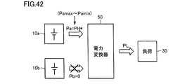
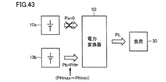
- the power converter is controlled so as to charge the DC power supply by making the sum of output powers from other DC power supplies excluding the DC power supply that has reached the constraint value higher than the required power of the load.
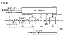
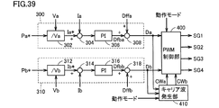
- the control device calculates the total input / output power from the first and second DC power supplies to the power line based on the deviation between the voltage detection value of the power line and the voltage command value, and changes the operation mode. Accordingly, the power distribution ratio between the first and second DC power supplies is switched. Further, the control device sets the first power command value of the first DC power source and the second power command value of the second DC power source according to the overall input / output power and the power distribution ratio, and also sets the first power Based on the deviation of the detected current value of the first DC power supply with respect to the first current command value obtained by dividing the command value by the output voltage of the first DC power supply, a first for controlling the output from the first DC power supply.
- the second duty ratio for controlling the output from the DC power source is calculated.
- the control device includes first and second obtained respectively according to the comparison of the first carrier wave and the first duty ratio, and the pulse width modulation by the comparison of the second carrier wave and the second duty ratio, respectively. On-off control signals for the first to fourth switching elements are generated based on the control pulse signal.
- the power distribution ratio is variably set in accordance with the operating state of the first and second DC power supplies in the first mode, while the first and second DC power supplies in the second mode. Fixed to a voltage based ratio.
- the control device calculates the first and second duty ratios for the first and second DC power supplies by current feedback control based on the first current command value, and In the second mode, current feedback control based on the second current command value is executed in one of the first and second DC power supplies, while current feedback control is performed in the other of the first and second DC power supplies.
- the first and second duty ratios are calculated by executing feedforward control based on the output voltage of the DC power supply and the voltage command value without executing the above.
- the control device in each of the first and second modes, the first control pulse signal obtained by comparing the first duty ratio and the first carrier wave, the second duty ratio and the second On-off control signals for the first to fourth switching elements are generated based on the second control pulse signal obtained by comparing the carrier waves. Further, in each of the first and second modes, the phase difference between the first carrier wave and the second carrier wave is determined by the pulse transition timing of the first control pulse signal and the pulse of the second control pulse signal. In accordance with the calculated first and second duty ratios, the control is variably controlled so as to match the transition timing of the first and second.
- the plurality of operation modes further include a fourth mode.
- the power converter performs DC voltage conversion between one DC power source of the first and second DC power sources and the power line by on / off control of the first to fourth switching elements.
- the first operation mode is the fourth mode
- the second operation mode is the first mode.
- the power distribution ratio is variably set according to the operating states of the first and second DC power supplies, whereas in the fourth mode, the total input / output power is determined only by the output from one of the power supplies. Is set to be secured.
- the control device sets a circulating power value for charging / discharging between the first DC power source and the second DC power source in the first mode.
- the first power command value is set so as to be limited within the power range set according to the operating state of the first DC power supply, according to the total input / output power, the power distribution ratio, and the circulating power value.
- the second power command value is set by subtracting the first power command value from the total input / output power.
- a power supply system including a power converter connected between a plurality of DC power supplies and a power line common to the plurality of DC power supplies, the efficiency of the entire system is improved, each DC power supply is overcharged,
- the operation mode of the power converter can be selected so as to achieve both protection from overdischarge.
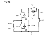
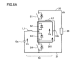
- FIG. 6 is a first circuit diagram illustrating a first circuit operation in a PB mode. It is a 2nd circuit diagram explaining the 1st circuit operation in PB mode.
- FIG. 10 is a first circuit diagram illustrating a second circuit operation in the PB mode.
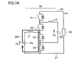
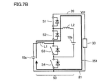
- FIG. 6 is a first circuit diagram illustrating DC / DC conversion (step-up operation) for the first DC power supply in the PB mode. It is a 2nd circuit diagram explaining DC / DC conversion (boost operation) with respect to the 1st direct-current power supply in PB mode.
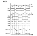
- FIG. 6 is a first circuit diagram illustrating DC / DC conversion (step-up operation) for a second DC power supply in the PB mode. It is a 2nd circuit diagram explaining the DC / DC conversion (step-up operation) with respect to the 2nd DC power supply in PB mode. It is a wave form diagram which shows the control operation example of the switching element of the power converter in PB mode.
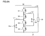
- FIG. 6 is a first circuit diagram illustrating a circuit operation in SB mode. It is a 2nd circuit diagram explaining the circuit operation
- FIG. 6 is a first circuit diagram illustrating DC / DC conversion (step-up operation) in the SB mode.
- FIG. 6 is a second circuit diagram illustrating DC / DC conversion (step-up operation) in the SB mode. It is a wave form diagram which shows the example of control operation of the switching element of the power converter in SB mode. It is a chart for explaining a logical operation expression for setting a control signal of each switching element in the SB mode.
- FIG. 4 is a chart for comparing the controllability of the power distribution ratio between the DC power sources in each operation mode shown in FIG. 3 and the settable range of the output voltage. It is a conceptual diagram for demonstrating the definition of the voltage range of a load request voltage. It is a chart for explaining selection of an operation mode in each voltage range. It is a functional block diagram which shows the control structure for the operation mode selection in the power converter in the power supply system according to Embodiment 1 of this invention. It is a 1st functional block diagram for demonstrating the function of an operation mode selection part. It is a conceptual diagram explaining the comparison between the operation modes of the converter loss estimated by the structure of FIG. It is a conceptual diagram explaining the comparison between the operation modes of the whole system loss estimated by the structure of FIG.
- FIG. It is a wave form diagram for demonstrating the operation example of the operation mode correction part shown in FIG. It is a graph which shows correction of the operation mode selection by the operation mode correction part in each voltage range. It is a conceptual diagram for demonstrating the 1st example of correction
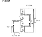
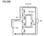
- FIG. 28 is a first circuit diagram illustrating a current path in a predetermined period of FIG. 27.
- FIG. 28 is a second circuit diagram illustrating a current path in a predetermined period of FIG. 27.
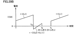
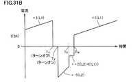
- FIG. 28 is a first current waveform diagram of the switching element at the current phase shown in FIG. 27.
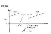
- FIG. 31 is a first current waveform diagram of the switching element at the current phase shown in FIG. 30.
- FIG. 31 is a second current waveform diagram of the switching element at the current phase shown in FIG. 30.
- FIG. 11 is a first block diagram for illustrating power converter control according to the second embodiment.
- FIG. 11 is a second block diagram for illustrating power converter control according to the second embodiment.
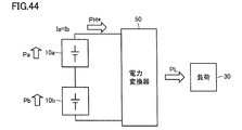
- FIG. 2 It is a conceptual diagram for demonstrating the power flow in the power supply system in the PB mode by the power converter control according to Embodiment 2.
- FIG. It is a table explaining the setting of control signals and control data in each operation mode belonging to the boost mode.
- It is a conceptual diagram for demonstrating the power flow in the power supply system in the aB mode by the power converter control according to Embodiment 2.
- FIG. It is a conceptual diagram for demonstrating the power flow in the power supply system in bB mode by the power converter control according to Embodiment 2.
- FIG. It is a conceptual diagram for demonstrating the power flow in the power supply system in SB mode by power converter control according to Embodiment 2.
- 46 is a chart for explaining a plurality of operation modes of the power converter shown in FIG. 45 and setting of control signals and control data in each operation mode.
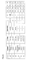
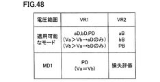
- 10 is a diagram for illustrating selection of an operation mode in each voltage range in the power supply system according to the third embodiment.
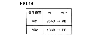
- 12 is a chart showing correction of operation mode selection by an operation mode correction unit in each voltage range in the power supply system according to the third embodiment.
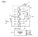
- FIG. 1 is a circuit diagram showing a configuration of a power supply system including a power converter according to the first embodiment of the present invention.
- power supply system 5 includes a plurality of DC power supplies 10a and 10b, a load 30, and a power converter 50.
- each of DC power supplies 10a and 10b is a secondary battery such as a lithium ion secondary battery or a nickel metal hydride battery, or a DC voltage excellent in output characteristics such as an electric double layer capacitor or a lithium ion capacitor. Consists of source elements.
- the DC power supply 10a and the DC power supply 10b correspond to a “first DC power supply” and a “second DC power supply”, respectively.
- DC power supplies 10a and 10b can be configured by DC power supplies of the same type and the same capacity, and can also be configured by DC power supplies having different characteristics and / or capacities.
- the power converter 50 is connected between the DC power supplies 10 a and 10 b and the power line 20.
- Power converter 50 controls a DC voltage (hereinafter also referred to as output voltage VH) on power line 20 connected to load 30 in accordance with voltage command value VH *. That is, the power line 20 is provided in common for the DC power supplies 10a and 10b.
- the load 30 operates by receiving the output voltage VH of the power converter 50.
- Voltage command value VH * is set to a voltage suitable for the operation of load 30.
- Voltage command value VH * may be variably set according to the operating state of load 30.
- the load 30 may be configured to be able to generate charging power for the DC power supplies 10a and 10b by regenerative power generation or the like.
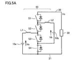
- the power converter 50 has a boost chopper circuit corresponding to each of the DC power supply 10a and the DC power supply 10b. That is, for DC power supply 10a, a current bidirectional first step-up chopper circuit having switching elements S1 and S2 as upper arm elements and switching elements S3 and S4 as lower arm elements is configured. Similarly, for the DC power supply 10b, a current bidirectional second step-up chopper circuit is configured with the switching elements S1 and S4 as upper arm elements and the switching elements S2 and S3 as lower arm elements. .
- the control device 40 generates control signals SG1 to SG4 for controlling on / off of the switching elements S1 to S4 in order to control the output voltage VH to the load 30.
- Va voltage
- Ia current
- Vb voltage
- Ib current
- Ib output voltage
- Ta and Tb detectors
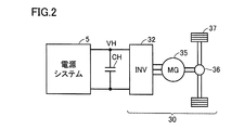
- FIG. 2 is a schematic diagram illustrating a configuration example of the load 30.
- load 30 is configured to include, for example, a traveling motor for an electric vehicle.
- Load 30 includes a smoothing capacitor CH, an inverter 32, a motor generator 35, a power transmission gear 36, and drive wheels 37.
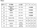
- PB mode a “parallel boost mode” in which DC / DC conversion is performed in parallel between DC power supplies 10 a and 10 b and power line 20, DC power supplies 10 a and 10 b and power line 20 connected in series are performed.
- SB mode series boost mode for performing DC / DC conversion with the.
- the PB mode corresponds to the “parallel connection mode” in Patent Document 3
- the SB mode corresponds to the “series connection mode” in Patent Document 3.
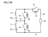
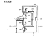
- direct connection mode of DC power supply 10a (hereinafter referred to as aD mode)” in which only DC power supply 10a is electrically connected to power line 20 and only DC power supply 10b is electrically connected to power line 20 “ "Direct connection mode (hereinafter referred to as bD mode) of DC power supply 10b”.
- the switching elements S1 and S4 are fixed on, while the switching elements S2 and S3 are fixed off.
- the DC power supply 10a is not used because it is kept disconnected from the power line 20.
- Va> Vb a short-circuit current is generated from the DC power supplies 10a to 10b via the diode D2. For this reason, Vb> Va is a necessary condition for applying the bD mode.
- the output voltage VH of the power line 20 is determined depending on the voltages Va and Vb of the DC power supplies 10a and 10b, and therefore must be directly controlled. Can not be. For this reason, in each mode included in the direct connection mode, the output voltage VH cannot be set to a voltage suitable for the operation of the load 30, so that the power loss in the load 30 may increase.
- the operating point 101 can be dealt with mainly by the output from the high-power DC power supply 10b.
- the operating point 102 can be dealt with mainly by the output from the high-capacity DC power supply 10a.
- DC power supplies 10a and 10b can be connected in parallel to power line 20 by turning on switching element S4 or S2.
- the equivalent circuit differs depending on the level of the voltage Va of the DC power supply 10a and the voltage Vb of the DC power supply 10b.
- the ON period and the OFF period of the lower arm element can be alternately formed by the ON / OFF control of the switching element S3.
- the ON and OFF periods of the lower arm element of the step-up chopper circuit can be alternately formed by controlling the switching elements S2 and S3 in common.
- the switching element S1 operates as a switch that controls regeneration from the load 30.
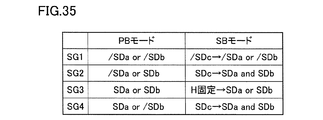
- the control signal SG3 of the switching element S3 is generated by the logical sum of the control pulse signals SDa and SDb.
- the switching element S3 functions as both the lower arm element of the boost chopper circuit (DC power supply 10a) of FIGS. 7A and 7B and the lower arm element of the boost chopper circuit (DC power supply 10b) of FIGS. 8A and 8B.
- On / off control is performed so as to realize
- the DC / DC conversion for inputting / outputting the DC power in parallel between the DC power supplies 10a, 10b and the power line 20 is executed, and then the output voltage VH is controlled to the voltage command value VH *. be able to. Furthermore, the input / output power of the DC power supply can be controlled according to the current command value of the DC power supply that is the target of current control.
- the DC power supply 10b is not used by the switching operation shown in FIGS. 7A and 7B, while bidirectional DC / DC conversion is performed between the DC power supply 10a and the power line 20 (load 30).
- the DC power supply 10a is not used by the switching operation shown in FIGS. 8A and 8B, while bidirectional DC / DC conversion is performed between the DC power supply 10b and the power line 20 (load 30). Is executed. Therefore, in the bB mode, switching elements S1 to S4 are controlled in accordance with control pulse signal SDb based on duty ratio Db for controlling the output of DC power supply 10b.
- FIG. 13 shows a waveform diagram for explaining an example of the control operation of the switching element in the SB mode.
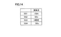
- control signals SG1 to SG4 can be set based on the logical operation of the control pulse signal SDc (/ SDc).
- the control pulse signal SDc is used as the control signals SG2 and SG4 of the pair of switching elements S2 and S4 constituting the lower arm element of the boost chopper circuit.
- control signal SG1 of switching element S1 constituting the upper arm element of the boost chopper circuit is obtained by control pulse signal / SDc.
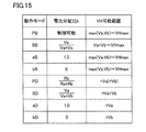
- FIG. 15 shows whether the power distribution ratio (k) can be controlled between the DC power supplies 10a and 10b in each operation mode shown in FIG. 3, and the settable range of the output voltage VH.
- the power distribution ratio k between DC power supplies 10a and 10b can be controlled by setting a current command value in a DC power supply that is a current control target.
- the output voltage VH can be controlled within a range from max (Va, Vb) which is the maximum value of the voltages Va and Vb to an upper limit voltage VHmax which is the control upper limit value of the output voltage VH.
- the output powers Pa and Pb of the DC power supplies 10a and 10b can be controlled independently. Can not. Further, the output voltage VH cannot be set lower than (Va + Vb). In the SB mode, the output voltage VH can be controlled within a range from (Va + Vb) to the upper limit voltage VHmax (Va + Vb ⁇ VH ⁇ VHmax).
- the range of the output voltage VH that can be output by the power converter 50 is different in each operation mode.
- the DC power supply can be controlled, while in other SB mode, SD mode, aB mode, bB mode, aD mode, bD mode, and PD mode, the DC power supply can be controlled.
- the power distribution between 10a and 10b cannot be arbitrarily controlled.
- the output voltage VH supplied to the load 30 needs to be set to a certain voltage or higher according to the operating state of the load 30.
- the output voltage VH corresponding to the DC link side voltage of the inverter 32 is a coil winding (not shown) of the motor generator 35. It is necessary to be higher than the induced voltage generated in (1).
- the torque range that can be output by the motor generator 35 changes according to the output voltage VH. Specifically, when the output voltage VH is increased, the torque that can be output also increases. Therefore, for example, output voltage VH needs to be within a voltage range in which motor generator 35 can output a torque corresponding to a torque command value determined by running control of the electric vehicle.
- the load minimum voltage corresponding to the minimum value of the output voltage VH for operating the load 30 according to the operating state of the load 30 (in the configuration example of FIG. 2, the torque and the rotational speed of the motor generator 35).
- VHmin can be predetermined. Therefore, the required load voltage VHrq can be determined in correspondence with the minimum load voltage VHmin.
- the current phase when the same torque is output varies depending on the DC link voltage (output voltage VH) of the inverter 32. Further, the ratio of the output torque to the current amplitude in the motor generator 35, that is, the motor efficiency changes according to the current phase. Therefore, when the torque command value of motor generator 35 is set, the optimum current phase at which the efficiency at motor generator 35 is maximized, that is, the power loss at motor generator 35 is minimized, corresponding to the torque command value. And an output voltage VH for realizing the optimum current phase can be determined. In the present embodiment, it is preferable that load request voltage VHrq is determined in consideration of the efficiency at load 30.
- the load request voltage VHrq related to the output voltage VH is set according to the operating state (for example, torque and rotation speed) of the load 30.
- the operating state for example, torque and rotation speed
- VH VHrq
- loss at the load 30 can be suppressed.
- the operating state of the load 30 it is also possible to set the load request voltage VHrq using the operating state (vehicle speed, accelerator opening, etc.) of the electric vehicle on which the motor generator 35 is mounted.
- VH ⁇ VHrq can be realized, that is, applicable operation modes differ depending on the range of the load request voltage VHrq set according to the operation state of the load 30.
- FIG. 16 shows the definition of the voltage range VR1 to VR3 of the load request voltage VHrq.
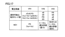
- FIG. 17 shows a chart for explaining the selection of the operation mode in each voltage range.
- load request voltage VHrq is in any of voltage ranges VR1 (VHrq ⁇ max (Va, Vb), VR2 (max (Va, Vb) ⁇ VHrq ⁇ Va + Vb), and VR3 (Va + Vb ⁇ VHrq ⁇ VHmax)). Is set.
- power converter 50 cannot output a voltage lower than max (Va, Vb). Therefore, when load request voltage VHrq is within voltage range VR1, output voltage VH is requested to be a load request. It cannot be matched with the voltage VHrq. Therefore, in the voltage range VR1, VH is brought as close to VHrq as possible in the range of VH ⁇ VHrq, and the aD mode, bD mode, and PD mode are selected as “applicable operation mode groups”.
- the output voltage VH can be controlled according to the voltage command value VH * as long as it is within the range of max (Va, Vb) to VHmax.
- the output voltage VH cannot be controlled lower than (Va + Vb). That is, the output voltage VH can be controlled according to the voltage command value VH * as long as it is within the range of (Va + Vb) to VHmax.
- the aB mode, bB mode, and PB mode are selected as applicable operation mode groups.
- the aD mode, bD mode, and PD mode cannot be applied.
- the SD mode satisfies the condition of VH ⁇ VHrq, it can be applied in the voltage range VR2.
- the SD mode can also be included in the applicable operation mode group in the voltage range VR2.
- the SB mode the difference between the output voltage VH and the load request voltage VHrq and the loss in the power converter 50 are larger than in the SD mode. Therefore, the applicable operation mode group in the voltage range VR2 Therefore, the SB mode is excluded.
- the PB mode, SB mode, aB mode, bB mode, and PB mode are selected as applicable operation mode groups in light of the controllable range of the output voltage VH in each operation mode described above.
- the PB mode, SB mode, aB mode, bB mode, and PB mode are selected as applicable operation mode groups in light of the controllable range of the output voltage VH in each operation mode described above.
- VH * VHrq.
- each direct connection mode (aD mode, bD mode, PD mode, and SB mode) cannot be applied.
- FIG. 18 is a functional block diagram showing a control configuration for selecting an operation mode in power converter 50 in the power supply system according to the first embodiment of the present invention.
- each block described in the following functional block diagrams including FIG. 18 are realized by software processing by the control device 40 by executing a predetermined program and / or hardware processing by operation of a dedicated electronic circuit. Shall be.
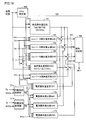
- operation mode control unit 150 for controlling operation mode selection in power converter 50 includes an operation mode selection unit 160 and an operation mode correction unit 170.
- the operation mode selection unit 160 minimizes the loss of the entire power supply system 5 based on the load request voltage VHrq determined according to the operation state of the load 30 and the operation states (power supply states) of the DC power supplies 10a and 10b.
- the operation mode (hereinafter referred to as “efficiency priority mode”) is selected, and the mode selection signal MD1 according to the selection result is generated. That is, the mode selection signal MD1 is a signal indicating which of the eight modes shown in FIG. 15 is selected as the “efficiency priority mode”.
- the power supply state includes, for example, voltages Va and Vb, currents Ia and Ib, temperatures Ta and Tb, and the like. Further, the output powers Pa and Pb of the DC power supplies 10a and 10b can be obtained from the total power PH and the power distribution ratio k. Thus, the efficiency priority mode corresponds to the “first operation mode”.
- the total power PH can be calculated in accordance with the power for ascending / descending determined according to the voltage difference between the output voltage VH of the power line 20 and the voltage command value VH *.
- the total power PH can be calculated by adding the load power PL consumed by the load 30.
- the load power PL can be estimated based on the operation state (rotation speed and torque) of the motor generator 35. Note that PL ⁇ 0 is indicated when the load 30 generates power (when the motor generator 35 is regenerated).
- the operation mode correction unit 170 is a mode selection instruction signal indicating a final operation mode selection result based on the mode selection signal MD1 from the operation mode selection unit 160 and the operation states and limit values of the DC power supplies 10a and 10b. MD * is generated.
- the mode selection instruction signal MD * is a signal indicating which of the eight modes shown in FIG. 15 has been selected as the final operation.
- Power converter 50 is applied with an operation mode according to mode selection instruction signal MD *, and performs DC / DC conversion between DC power supplies 10 a and / or 10 b and power line 20.
- the constraint values (power constraint values) of the DC power supplies 10a and 10b are the power upper limit value Pamax and the power lower limit value Pamin of the DC power supply 10a, the power upper limit value Pbmax and the power lower limit value Pbmin of the DC power supply 10b, and the DC power supplies 10a and 10b.
- SOCmax indicating the SOC upper limit value
- SOCmin indicating the SOC lower limit value.
- SOCmax and SOCmin are values common to DC power supplies 10a and 10b, but the SOC upper and lower limit values may be determined separately for each DC power supply.
- Each power upper limit value indicates the upper limit value of the discharge power, and is set to 0 or positive.
- each power lower limit value indicates the upper limit value of the charging power, and is set to 0 or negative.
- the power lower limit value is set to 0, it means that charging of the DC power supply is prohibited.
- the power upper limit Pamax and the power lower limit Pamin are set based on the SOC (State of Charge) and / or the temperature Ta of the DC power supply 10a.
- power upper limit Pbmax and power lower limit Pbmin can be set for DC power supply 10b.
- the load power PL needs to be limited within the range of PHmax to PHmin. That is, the operation command value for the load 30 to perform the regenerative operation or the power running operation is generated by limiting the load power PL within a range where PHmin ⁇ PL ⁇ PHmax.
- the load power PL by the motor generator 35 is determined by the product of the torque and the rotational speed, so that the torque command value is limited as necessary.
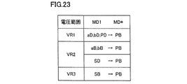
- the operation mode correction unit 170 cancels the selection of the operation mode (efficiency priority mode) by the mode selection signal MD1 when the SOC and / or output power reaches the power supply constraint value in at least one of the DC power supplies 10a and 10b.
- the mode selection instruction signal MD * is generated so as to select an operation mode (PB mode) capable of controlling the power distribution between the DC power supplies 10a and 10b. That is, MD * ⁇ MD1.
- operation mode correction unit 170 maintains selection of an operation mode (efficiency priority mode) based on mode selection signal MD1 when the SOC and output power have not reached the power supply constraint values.
- mode selection instruction signal MD * MD1
- MD * MD1
- the operation mode selected by the operation mode correction unit 170 instead of the efficiency priority mode corresponds to the “second operation mode”.
- FIG. 19 is a functional block diagram for explaining the function of the operation mode selection unit 160 in the voltage range VR2.
- operation mode selection unit 160 includes load loss estimation units 161 and 165, converter loss estimation units 162 to 164, 166, internal resistance estimation units 171a and 171b, and power supply loss estimation units 172 to 174. 176, and a loss comparison unit 168.
- the VHrq setting unit 190 sets the load request voltage VHrq according to the operating state of the load 30.
- the load request voltage VHrq can be determined based on the rotation speed and torque of the motor generator 35.
- the output voltage VH needs to be controlled to be equal to or higher than the load request voltage VHrq.
- the VHrq setting unit 190 corresponds to a “required voltage setting unit”.
- the aB mode, bB mode, PB mode, and SD mode are included in the applicable operation mode group.
- the operation mode selection unit 160 selects an efficiency priority mode from these operation mode groups.
- the output voltage VH is (Va + Vb), which is higher than the load request voltage VHrq.
- Converter loss estimation unit 162 estimates converter loss Plcv in power converter 50 when the aB mode is applied.
- Converter loss estimation unit 163 estimates converter loss Plcv in power converter 50 when the bB mode is applied.
- VHrq VH in bB mode
- PH Pb in bB mode
- an estimated value of converter loss Plcv in the bB mode is calculated according to an arithmetic expression.
- Converter loss estimation unit 164 estimates converter loss Plcv in power converter 50 when the PB mode is applied.
- the output powers Pa and Pb can be obtained from the total power PH and the power distribution ratio k.
- the power distribution ratio k at this time is, for example, a map created in advance based on the state of the DC power supplies 10a and 10b (for example, SOC balance or upper / lower limit power balance), output power level (PH), or the like. It can be decided by referring to.
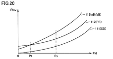
- FIG. 20 is a schematic diagram for explaining comparison between converter loss operation modes.
- the converter loss in the voltage range VR2 estimated by the configuration of FIG. 19 is compared.
- the horizontal axis indicates the total power PH
- the vertical axis indicates the converter loss Plcv.
- the converter loss Plcv increases as the total power PH increases, but the characteristics differ between the operation modes. Changes in converter loss Plcv in the SD mode, PB mode, and aB or bB mode with respect to changes in total power PH are indicated by characteristic lines 111 to 113, respectively.
- the magnitude of the converter loss Plcv changes according to the level of the total power PH. Except for the low load region (region of PH ⁇ Pt in FIG. 20), the current in the DC / DC conversion by each of the DC power sources 10a and 10b, which has been described with reference to FIGS. In the mode, the converter loss Plcv tends to be smaller than that in the aB / bB mode.
- iron loss occurs in both reactors L1 and L2
- the aB / bB mode iron loss occurs in only one of reactors L1 and L2. For this reason, in the low load region, the influence of the iron loss of the reactor on the total power PH becomes large, and therefore the converter loss Plcv tends to be smaller in the aB / bB mode than in the PB mode.
- the converter loss Plcv in each operation mode can be estimated based on the voltages Va and Vb of the DC power supplies 10a and 10b, the output voltage VH (VHrq), and the total power PH.
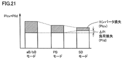
- FIG. 21 is a schematic diagram for comparing the sum of converter loss and load loss between operation modes.
- the converter loss Plcv is minimized in the SD mode. For this reason, when the increase amount ⁇ Plld of the load loss due to the application of the SD mode exceeds the decrease amount of the converter loss Plcv, the sum of the converter loss Plcv and the load loss Plld becomes the minimum in the SD mode. As a result, in the example of FIG. 21, the SD mode is effective as the efficiency priority mode.
- the converter loss Plcv and the load loss Plld change due to changes in the operating state of the load 30 and the DC power supplies 10a and 10b, so that the efficiency operation mode in which the sum of these losses is minimized also changes. . Therefore, in order to accurately select the efficiency priority mode, it is preferable to estimate the converter loss Plcv and the load loss Plld for each operation mode according to the current operation state, as shown in FIG. Even if the total power PH is the same, the loss (power loss) caused by the internal resistance in the DC power supplies 10a and 10b changes according to the operation mode selection. In particular, in the PB mode, it can be expected that the power loss is reduced due to the dispersion effect of the currents Ia and Ib. For this reason, it is preferable to estimate the power loss Plps for each operation mode according to the current operation state.
- internal resistance estimating unit 171a estimates internal resistance value Ra of DC power supply 10a according to temperature Ta and SOCa indicating the state of DC power supply 10a.
- internal resistance estimation unit 171b estimates internal resistance value Rb of DC power supply 10b according to temperature Tb and SOCb indicating the state of DC power supply 10b.
- the functions of the internal resistance estimation units 171a and 171b can be realized by creating in advance a map that reflects the characteristic relationship between the temperature and SOC and the internal resistance value, which is obtained by actual machine experiments or the like.
- the power loss estimation unit 176 estimates power loss Plps when the SD mode is applied.
- the estimated value of the power loss Plps in the SD mode can be calculated according to a preset map or arithmetic expression as a function of the estimated internal resistance values Ra, Rb (Ra + Rb), the total power PH, and the voltage (Va + Vb).
- the power loss estimation unit 172 estimates power loss Plps when the aB mode is applied.
- the power loss estimation unit 173 estimates the power loss Plps when the bB mode is applied.
- the power loss estimator 174 estimates the power loss Plps when the PB mode is applied.
- the estimated value of the power supply loss Plps in the PB mode is calculated according to a preset map or arithmetic expression as a function of the estimated internal resistance values Ra and Rb and the output powers Pa and Pb calculated from PH and k. be able to.
- the aB mode is selected. A total loss Ptl is estimated.
- the load loss Plld calculated by the load loss estimator 161, the converter loss Plcv estimated by the converter loss estimator 163, and the power loss Plps calculated by the power loss estimator 173 are used to calculate the bB mode. A total loss Ptl at the time of selection is estimated.
- the PB mode selection is performed based on the sum of the load loss Plld estimated by the load loss estimation unit 161, the converter loss Plcv estimated by the converter loss estimation unit 164, and the power loss Plps calculated by the power loss estimation unit 174. The total loss Ptl at the time is calculated. Further, the SD mode selection is performed based on the sum of the load loss Plld estimated by the load loss estimation unit 165, the converter loss Plcv estimated by the converter loss estimation unit 166, and the power loss Plps calculated by the power loss estimation unit 176. The total loss Ptl at the time is calculated.
- the loss comparison unit 168 compares the estimated total loss Ptl in each of the ab mode, bB mode, PB mode, and SD mode as the efficiency priority mode. select. Further, the loss comparison unit 168 generates a mode selection signal MD1 for indicating the efficiency priority mode.
- operation mode selection unit 160 selects the efficiency priority mode according to the total loss evaluation by the configuration shown in FIG. 17 again, in voltage range VR2, operation mode selection unit 160 selects the efficiency priority mode according to the total loss evaluation by the configuration shown in FIG. 17 again, in voltage range VR2, operation mode selection unit 160 selects the efficiency priority mode according to the total loss evaluation by the configuration shown in FIG. 17 again, in voltage range VR2, operation mode selection unit 160 selects the efficiency priority mode according to the total loss evaluation by the configuration shown in FIG.
- the operation mode control unit 150 selects an operation mode from the aD mode, bD mode, and PD mode included in the applicable operation mode group.
- the aD mode when Va> Vb
- the bD mode when Vb> Va
- the operation mode is designated by the mode selection instruction signal MD *.
- the SB mode can be selected as the efficiency priority mode from among the PB mode, SB mode, aB mode, and bB mode included in the applicable operation mode group.
- the power loss Plps may be suppressed by the dispersion effect of the currents Ia and Ib, which exceeds the current reduction effect of the SB mode. Therefore, it is preferable to estimate the total loss Ptl for each operation mode in the voltage range VR3 according to the current operation state.
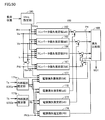
- FIG. 50 is a functional block diagram for explaining the function of the operation mode selection unit 160 in the voltage range VR3.
- operation mode selection unit 160 includes converter loss estimation units 162 to 164, 167, internal resistance estimation units 171a and 171b, power supply loss estimation units 172 to 174, 177, and loss comparison unit 168. including.
- Converter loss estimation unit 162 to 164 similar to FIG. 19 estimates converter loss Plcv when aB mode, bB mode, and PB mode are applied based on a preset map or arithmetic expression based on the current operating state.
- Converter loss estimation unit 167 calculates an estimated value of converter loss Plcv in the SB mode according to a preset map or arithmetic expression as a function of voltage Va + Vb, load request voltage VHrq, and total power PH.
- the power loss estimator 177 estimates the converter loss Plcv in the SB mode as a function of the estimated internal resistance Ra, Rb (Ra + Rb), voltage Va + Vb and total power PH according to a preset map or arithmetic expression. Is calculated.
- the total loss Ptl when the aB mode is selected is estimated by the sum of the converter loss Plcv calculated by the converter loss estimation unit 162 and the power supply loss Plps calculated by the power supply loss estimation unit 172.
- the total loss Ptl when the bB mode is selected is estimated based on the sum of the converter loss Plcv estimated by the converter loss estimation unit 163 and the power supply loss Plps calculated by the power supply loss estimation unit 173.
- the total loss Ptl when the PB mode is selected is calculated based on the sum of the converter loss Plcv estimated by the converter loss estimation unit 164 and the power supply loss Plps calculated by the power supply loss estimation unit 174.
- the total loss Ptl at the time of selecting the SB mode is calculated by the sum of the converter loss Plcv estimated by the converter loss estimation unit 167 and the power supply loss Plps calculated by the power supply loss estimation unit 177.
- the loss comparison unit 168 sets the operation mode that minimizes the total loss Ptl as the efficiency priority mode by comparing the total loss Ptl in the ab mode, bB mode, PB mode, and SB mode estimated in this way.
- a mode selection signal MD1 for indicating the selected efficiency priority mode is generated.
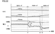
- FIG. 22 is a waveform diagram showing an operation example of the operation mode correction unit 170.
- FIG. 22 shows an operation example in the voltage range VR3.
- SB mode selected as the efficiency priority mode in voltage range VR3 is applied, and power converter 50 operates.
- the power Pa, Pb (Pa> 0, Pb> 0) is output from the DC power supplies 10a, 10b at a constant rate according to the power distribution ratio k uniquely determined by the voltages Va, Vb. Power is supplied to 30.
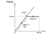
- the output power Pa of the DC power supply 10a has a sufficient margin with respect to the power upper limit Pamax.
- FIG. 22 shows an operation when the full charge capacity of the DC power supply 10b is smaller than the full charge capacity of the DC power supply 10b. For this reason, while the output powers Pa and Pb are substantially equal, the SOC (SOCb) of the DC power supply 10b decreases at a faster rate than the SOC (SOCa) of the DC power supply 10a.
- SOCb reaches the SOC lower limit value SOCmin, which is one of the power supply constraint values. For this reason, from the viewpoint of power supply protection, it is necessary to stop the discharge from the DC power supply 10b.
- the operation mode correction unit 170 changes the mode selection instruction signal MD * so as to select the PB mode that can control the power distribution between the DC power supplies 10a and 10b, instead of the SB mode that is the efficiency priority mode. Set.
- the DC power supply 10b whose SOC has reached the power supply constraint value is charged by the surplus of Pa with respect to the load power PL. (Pb ⁇ 0).
- Pb ⁇ 0
- such an operation can be realized by setting a current command value of a DC power source that is an object of current control.
- SOCa continues to decrease gradually, while SOCb starts to increase.
- the operating state of the load 30 changes, and regenerative power from the load 30 is supplied to the power line 20.
- regenerative power generation is started by operating the brake pedal in the electric vehicle on which the motor generator 35 is mounted.
- both DC power supplies 10a and 10b are charged.
- the distribution of the charging power of the DC power supplies 10a and 10b at this time can also be controlled in the PB mode.
- the correction of the operation mode selection by the operation mode correction unit 170 is completed at time t3.
- the SB mode that is the efficiency priority mode is selected again, and the power converter 50 operates.
- the operation mode selection is completed, it is preferable to prevent the occurrence of so-called chattering in which the operation mode is switched to the PB mode again immediately after returning to the efficiency priority mode. For example, immediately after returning to the efficiency priority mode (SB mode), when the output power reaches the power supply limit value on at least one of the DC power supplies 10a and 10b, the PB mode is selected again for power supply protection. Causes chattering.
- SB mode efficiency priority mode
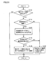
- FIG. 51 is a flowchart for explaining the control process when the correction of the operation mode selection is finished. For example, when the control device 40 executes a program stored in advance, a series of control processing according to the flowchart is executed by the operation mode correction unit 170 for each control cycle.
- control device 40 (operation mode correction unit 170) performs the following steps S110 to S150 to prevent chattering during correction of operation mode selection (when YES is determined in S100). Execute.
- the operation mode correction unit 170 maintains the correction of the operation mode in step S150. Then, the PB mode is selected. Furthermore, even if the DC power supplies 10a and 10b are restored from the state where the DC power supplies 10a and 10b are applied to the power supply constraint values (when YES is determined in S110), the operation mode correction unit 170 is the power command values Pa * and Pb when the efficiency priority mode is applied. When the estimated value of * has reached the power supply constraint value (NO in S130), the process proceeds to step S150, and the correction of the operation mode is maintained. In this case, when the correction of the operation mode selection is finished and the efficiency priority mode is applied, the operation mode is corrected again for power supply protection, and chattering occurs.
- the operation mode correction unit 170 operates when the operation mode correction ends by controlling whether to end the operation mode correction and return to the efficiency priority mode according to the flowchart shown in FIG. It is possible to prevent the mode from chattering.
- the aD mode, the bD mode, or the PD mode has the voltages Va and Vb.
- the efficiency priority mode is selected.
- operation mode correction unit 170 generates mode selection instruction signal MD * so as to select the PB mode.
- the efficiency priority mode is selected in accordance with the total loss evaluation described with reference to FIGS.
- the SOC and / or input / output power of the DC power supply 10a reaches the power supply restriction value when the aB mode is selected, or the SOC and / or input / output power of the DC power supply 10b becomes the power supply restriction value when the bB mode is selected.
- the operation mode correction unit 170 If it has been reached, the operation mode correction unit 170 generates a mode selection instruction signal MD * so as to select the PB mode.
- the SB mode is selected as the efficiency priority mode. Then, when the SOC and / or the output power reaches the power supply constraint value in any of DC power supplies 10a and 10b when the SB mode is selected, operation mode correction unit 170 selects mode selection instruction signal MD so as to select the PB mode. * Is generated.
- the operation mode correction unit 170 corrects the operation mode selection so as to select the PB mode instead of the efficiency priority mode. As a result, it is possible to supply the total power PH even in the range of PH> Pamax while maintaining Pa ⁇ Pamax, that is, while protecting the DC power supply 10a from overpower.
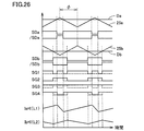
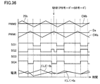
- FIG. 26 shows an example of control operation in the PB mode when a phase difference is intentionally provided between the carrier waves CWa and CWb.
- the control signals SG1 to SG4 in FIG. 26 have waveforms different from the control signals SG1 to SG4 in FIG. From the comparison between FIG. 9 and FIG. 26, it is understood that the phase relationship (current phase) between the current I (L1) and the current I (L2) changes by changing the phase difference ⁇ between the carrier waves CWa and CWb. Is done.
- the switching loss of the switching elements S1 to S4 is reduced by carrier phase control that appropriately adjusts the phase difference ⁇ between the carrier waves CWa and CWb.
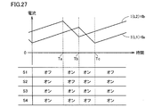
- the switching element S2 is turned off, so that the lower arm element of the step-up chopper circuit is turned off with respect to the DC power supply 10b. Therefore, the current I (L2) starts to decrease. Instead of switching off the switching element S2, the switching element S1 is turned on.
- the current phase that is, the phase difference ⁇ between the carrier waves CWa and CWb is set so that the falling start timing (maximum point) of the current I (L1) and the rising timing (minimum point) of the current I (L2) overlap. adjust.
- switching element S2 is turned on and switching element S4 is turned off.
- switching element S1 is turned off and switching element S4 is turned on.
- the lower arm element of the step-up chopper circuit is turned on for each of the DC power supplies 10a and 10b.
- both currents I (L1) and I (L2) rise.
- I (S4) I (L1) in the period up to time Ta and the period after time Tc.
- I (S4) ⁇ (I (L2) ⁇ I (L1)).
- I (S4) 0.
- both the currents I (L1) and I (L2) increase.
- the switching element S4 is turned off at time Tx, whereby the current I (L1) starts to decrease.
- the switching element S1 is turned on instead of the switching element S4 being turned off.
- I (S2) ⁇ (I (L1) ⁇ I (L2)).
- I (S2) ⁇ I (L1).
- phase difference ⁇ between the carrier waves CWa and CWb
- loss in the switching elements S1 to S4 can be reduced.
- the current I (L1) starts to fall (maximum point) and the current I (L2) rises (minimum point).
- the phase difference ⁇ so that they overlap, that is, the turn-on timing of the switching element S2 and the turn-off timing of the switching element S4 coincide with each other, loss in the switching elements S1 to S4 is suppressed.
- phase difference ⁇ the falling timing (or rising timing) of the control pulse signal SDa and the rising timing (or falling timing) of the control pulse signal SDb overlap.
- the pulse transition timing of the control pulse signal SDa matches the pulse transition timing of the control pulse signal SDb.
- the transition timing indicates the timing at which the H level / L level of the pulse is switched.
- phase difference ⁇ at which the current phase as shown in FIG. 27 can be realized that is, the phase difference ⁇ by the carrier phase control is also determined according to the duty ratios Da and Db.
- phase difference map the relationship between the duty ratios Da and Db and the phase difference ⁇ by the carrier phase control is obtained in advance, and the corresponding relationship is preliminarily mapped (hereinafter also referred to as “phase difference map”) or a function equation (hereinafter referred to as “level” It can be stored in the control device 40 as a “phase difference calculation formula”.
- the phase difference ⁇ for carrier phase control can be calculated based on the calculated duty ratios Da and Db. Then, by generating the carrier waves CWa and CWb so as to have the calculated phase difference ⁇ , high-efficiency DC / DC conversion with suppressed loss in the switching elements S1 to S4 can be realized.
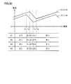
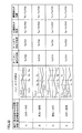
- FIG. 32 is a chart for explaining carrier phase control according to the first embodiment of the present invention in each operation state of the DC power supply.
- the DC power supply 10a is in a power running state, while the DC power supply 10b is in a regenerative state.
- the carrier wave has a current phase such that the rising timing (minimum point) of the current I (L1) and the rising timing (maximum point) of the current I (L2) overlap at Tc in the figure. Adjust the phase difference ⁇ .
- the turn-on loss of the switching element S1 and the turn-off loss of the switching element S3 at Tc can be reduced.
- the conduction loss of the switching element S1 during the period Tb to Tc and the conduction loss of the switching element S3 during the period Tc to Ta can be reduced.
- the loss in the switching elements S1 to S4 can be reduced.
- the phase difference ⁇ for reducing the loss in the switching elements S1 to S4 differs depending on the combination of the power running / regenerative state of the DC power supplies 10a and 10b. Therefore, it is preferable to set the above-described phase difference map or phase difference calculation formula for each power running / regenerative state combination (states A to D in FIG. 32).
- the above-described carrier phase control can be combined in the DC / DC conversion in the PB mode for controlling the output voltage VH to the voltage command value VH *.
- the loss of the switching elements S1 to S4 can be reduced by maximally enjoying the effect of canceling out the currents in the DC / DC conversion by the DC power sources 10a and 10b described with reference to FIGS. 7A to 8B.
- highly efficient DC / DC conversion can be performed.
- the positions of the carrier waves CWa and CWb are such that the falling timing of the control pulse signal SDa and the rising timing of the control pulse signal SDb, or the rising timing of the control pulse signal SDa and the falling timing of the control pulse signal SDb overlap.
- the phase difference ⁇ By setting the phase difference ⁇ , the rising timing (minimum point) and falling timing (maximum point) between the currents I (L1) and I (L2) shown in the states A and B of FIG. The current phase at the same timing is realized.
- control signal SG3 in the PB mode is generated based on the logical sum of control pulse signals SDa and SDb. Therefore, when the phase difference ⁇ is set so that the falling (or rising) timing of the control pulse signal SDa and the rising (or falling) timing of the control pulse signal SDb overlap, when VH> (Va + Vb) is satisfied, It is understood that the ratio of the H level period of the control signal SG3 in the PB mode exceeds 1.0. That is, when VH> (Va + Vb), the control signal SG3 is fixed to the H level also by PWM control common to the PB mode with the duty ratios Da and Db.
- the control signal SG1 in the PB mode is generated based on the logical sum of the control pulse signals / SDa and / SDb.
- the phase difference ⁇ is set as described above, the rising timing of the control pulse signal / SDa and the rising timing of the control pulse signal / SDb overlap. Therefore, the duty ratio DSG1 of the control signal SG1 is represented by (1 ⁇ Da) + (1 ⁇ Db). That is, DSG1 is expressed by the following equation (7).
- control signals SG2 and SG4 in the SB mode are inverted signals of the control signal SG1.
- the logical operation result of not (/ SDb or / SDa) is the logical product (SDb and SDa) of SDa and SDb. Therefore, control signals SG2 and SG4 to be set according to control pulse signal SDc can also be generated based on the logical operation of control pulse signals SDa and SDb.
- control signals SG1 to SG4 to be set based on the duty ratio Dc in the SB mode are It can be generated from the control pulse signals SDa and SDb based on the duty ratios Da and Db.
- control signal SG3 is a signal fixed at the H level by the logical sum of the control pulse signals SDa and SDb.
- Control signal SG1 can be generated to have a duty equivalent to that of PWM control based on duty ratio Dc by the logical sum of control pulse signals / SDa and / SDb.
- the control signals SG2 and SG4 set complementarily to the control signal SG1 can also be generated by the logical product of the control pulse signals SDa and SDb.
- phase difference ⁇ in the SB mode also follows a preset phase difference map or phase difference calculation formula that stores the relationship between the duty ratios Da and Db and the phase difference ⁇ , as in the carrier phase control in the PB mode. , And can be calculated based on the duty ratios Da and Db calculated in the SB mode.
- FIG. 36 shows a waveform diagram showing an operation example of the PB mode and the SB mode in the power converter control according to the modification of the first embodiment.
- a switch command from the PB mode to the SB is issued at the peak of the carrier wave CWa.
- control signals SG1 to SG4 are generated based on the duty ratios Da and Db calculated by the current control of the DC power supplies 10a and 10b.
- the control signal in the SB mode is immediately calculated based on the control pulse signals SDa and SDb at that time without newly calculating the duty ratio Dc according to the logical operation expression shown in FIG. SG1 to SG4 can be generated.
- control signals SG1 to SG4 in the SB mode can be generated using the duty ratios Da and Db in common with other operation modes belonging to the boost mode including the PB mode.
- the switching process between the PB mode and the SB mode can be executed without causing a control delay.
- FIG. 37 is a diagram illustrating a basic concept of power converter control according to the second embodiment.
- output voltage VH increases in a state where total power PH is larger than load power PL (PH> PL), but decreases in a state where PH ⁇ PL. Therefore, in the power converter control according to the second embodiment, the command value of total power PH is set according to voltage deviation ⁇ VH with respect to voltage command value VH * of output voltage VH. Further, by distributing the total power PH between the output powers Pa and Pb, the outputs of the DC power supplies 10a and 10b are subjected to power control (current control).
- FIG. 38 and 39 are block diagrams for illustrating power converter control according to the first embodiment.
- FIG. 38 shows a configuration for a control calculation for setting the power command value of each DC power supply
- FIG. 39 shows a control calculation for controlling the output of each DC power supply in accordance with the set power command value. The configuration of is shown.
- control device 40 includes a voltage control unit 200 and a power management unit 290.
- the power management unit 290 determines the power upper limit value PHmax and the power lower limit value PHmin related to the total power PH, the power upper limit value Pamax and the power lower limit value of the DC power supply 10a based on the operating state of the DC power supplies 10a and 10b and / or the load 30. Pamin and power distribution ratio k between DC power supplies 10a and 10b are set.
- the power distribution ratio k in the PB mode, can be set to an arbitrary value of 0 ⁇ k ⁇ 1.0. As described above, the power distribution ratio k can be determined based on, for example, the state of the DC power supplies 10a and 10b (for example, SOC balance or upper / lower limit power balance), output power level (PH), or the like. . As will be described in detail later, the power distribution ratio k is switched according to the operation mode.
- the power management unit 290 further sets a circulating power value Pr for charging / discharging between the DC power supplies 10a and 10b.
- the circulating power value Pr corresponds to the output power from the DC power supply 10a for charging the DC power supply 10b.
- the DC power supply 10b can be charged while the total power PH is supplied to the power line 20 by the output power of the DC power supply 10a.
- the DC power supply 10a can be charged while the total power PH is supplied to the power line 20 by the output power of the DC power supply 10b.
- the power management unit 290 sets the circulating power value Pr so as to promote the charging of the DC power supply on the low SOC side.
- the voltage controller 200 sets the power command values Pa * and Pb * of the DC power supplies 10a and 10b based on the voltage deviation of the output voltage VH.
- the voltage control unit 200 includes a deviation calculation unit 210, a control calculation unit 220, a limiter 230, a power distribution unit 240, a circulating power addition unit 250, a limiter 260, and a subtraction unit 270.
- the control calculation unit 220 calculates the total power PHr required for voltage control based on the voltage deviation ⁇ VH. For example, the control calculation unit 220 sets PHr according to the following equation (10) by PI calculation.
- Kp Kp ⁇ ⁇ VH + ⁇ (Ki ⁇ ⁇ VH) (10)
- Ki is an integral control gain.
- the load power PL can be predicted from the operating state of the load 30, it is also possible to set the total power PHr required according to the equation (11) by further reflecting this predicted value PL *. In this way, the output voltage VH can be controlled in a form that feeds forward power consumption at the load 30.
- the power distribution unit 240 calculates the output power k ⁇ PH * that the DC power supply 10a should share based on the total power command value PH * and the power distribution ratio k.
- FIG. 40 is a conceptual diagram for explaining the power flow in the power supply system according to the power command value set according to FIG.
- the DC power supply 10b is charged by the output power from the DC power supply 10a (Pr> 0), or the DC power supply 10a is charged by the output power from the DC power supply 10b (Pr ⁇ 0). )can do.
- the DC power supply 10a can be protected from overpower. That is, overcharge and overdischarge of the DC power supply 10a can be prevented.
- the load power PL is limited within the range of PHmin to PHmax, and the total power command value PH * is surely limited within the range of PHmax to PHmin by the limiter 230, so that the DC power supply 10b is also protected from overpower. Can protect. That is, overcharge and overdischarge of the DC power supply 10b can be prevented.
- control device 40 controls current control unit 300, current control unit 310, PWM (Pulse Width Modulation) for controlling the output from DC power supplies 10a, 10b in accordance with power command values Pa *, Pb *. )
- Control unit 400 and carrier wave generation unit 410 controls the output of the DC power supply 10a by current control.
- the current control unit 310 controls the output of the DC power supply 10a by current control.
- the current controller 300 includes a current command generator 302, a deviation calculator 304, a control calculator 306, and an FF adder 308.
- the control calculation unit 306 calculates a control amount Dfba for current feedback control based on the current deviation ⁇ Ia. For example, the control calculation unit 306 calculates the control amount Dfba according to the following equation (12) by PI calculation.
- the FF adder 308 calculates the duty ratio Da related to the output control of the DC power supply 10a by adding the FB control amount Dfba and the FF control amount Dffa.
- the duty ratio Da is the lower arm element of the step-up chopper circuit (FIG. 7A, FIG. 7B) when performing DC / DC conversion between the voltage Va of the DC power supply 10a and the output voltage VH, as in the equation (1). This corresponds to the duty ratio during which the switching elements S3 and S4 are turned on.
- the current control unit 310 corresponding to the DC power supply 10b includes a current command generation unit 312, a deviation calculation unit 314, a control calculation unit 316, and an FF addition unit 318.
- the control calculation unit 316 calculates a control amount Dfbb for current feedback control based on the current deviation ⁇ Ib. For example, the control calculation unit 316 calculates the control amount Dfbb according to the following equation (14) by PI calculation.
- voltage command value VH * may be a detected value of output voltage VH.
- the FF adder 318 calculates the duty ratio Db related to the output control of the DC power supply 10b by adding the FB control amount Dfbb and the FF control amount Dffb.
- the duty ratio Db corresponds to the duty ratio during the period when the lower arm elements (switching elements S2 and S3) of the boost chopper circuit (FIGS. 8A and 8B) are turned on, as in Expression (2).
- the PWM control unit 400 controls the switching elements S1 to S4 by pulse width modulation control based on the duty ratios Da and Db set by the current control units 300 and 310 and the carrier waves CWa and CWb from the carrier wave generation unit 410.
- Control signals SG1 to SG4 are generated. Since pulse width modulation control and generation of control signals SG1 to SG4 by PWM control unit 400 are performed in the same manner as described with reference to FIGS. 9 and 10, detailed description thereof will not be repeated.
- Carrier wave generation unit 410 preferably generates carrier waves CWa and CWb by applying the carrier phase control described in the modification of the first embodiment.
- the power converter control according to the second embodiment in the DC / DC conversion in the PB mode, the voltage deviation of the output voltage VH is converted into the power command value, and the output of each DC power supply 10a, 10b. , The output voltage VH can be controlled to the voltage command value VH *. Thereby, each DC power supply 10a, 10b can be reliably protected from overpower on an output power basis. Further, it is possible to easily control the power distribution ratio k and the circulating power value Pr between the DC power supplies 10a and 10b.
- the power command value can be directly limited to one of the DC power supplies 10a and 10b. 12A and 12B, the limiter 260 can reliably limit the power command value Pa * of the DC power supply 10a within the range of Pamin ⁇ Pa * ⁇ Pamax. Thereby, the overpower of DC power supply 10a can be prevented strictly.
- the total power command value PH * is limited to within the range of PHmin to PHmax to set the power command value Pb * of the DC power supply 10b, and the load power PL is limited to within the range of PHmin to PHmax.
- the power supply 10b can also be indirectly protected from overpower.
- the DC power supply 10a in which the power command value Pa * is directly limited by the limiter 260 is more strictly protected from overpower than the DC power supply 10b. Therefore, it is preferable that the limiter 260 directly limit the power command value of the DC power source that requires more strict protection from overpower.
- FIG. 41 is a chart for explaining the setting of control signals and control data in each operation mode belonging to the boost mode.
- control configurations shown in FIGS. 38 and 39 are shared in each operation mode in the boost mode. Then, by changing the power distribution ratio k, the DC power source to be subjected to the current feedback control, and the arithmetic logic of the control signals SG1 to SG4, the difference in the operation mode is dealt with.
- the power distribution ratio k can be arbitrarily set within the range of 0 ⁇ k ⁇ 1.0, and the circulating power value Pr is also set to an arbitrary value in terms of control. can do.
- both currents Ia and Ib of DC power supplies 10a and 10b are controlled according to current command values Ia * and Ib * set based on a power command value for controlling output voltage VH. Is done.
- the DC power supply 10b is not used by the boost chopper circuit formed by the switching elements S1 to S4 by the switching operation shown in FIGS. 7A and 7B, while the DC power supply 10a and the power line 20 (load 30) are not used. Bidirectional DC / DC conversion is performed between them. Therefore, in the aB mode, switching elements S1 to S4 are controlled in accordance with control pulse signal SDa based on duty ratio Da for controlling the output of DC power supply 10a. Specifically, switching elements S3 and S4 constituting the lower arm element of the step-up chopper circuit shown in FIGS. 7A and 7B are commonly turned on / off in accordance with control pulse signal SDa. Similarly, switching elements S1 and S2 constituting the upper arm element of the step-up chopper circuit are commonly turned on / off in accordance with control pulse signal / SDa.
- the total power command value is calculated based on the voltage deviation ⁇ VH of the output voltage VH by the deviation calculating unit 210, the control calculating unit 220, and the limiter 230 in the same manner as in the PB mode.
- PH * is set. Since DC power supply 10b is not used, power upper limit PHmax and power lower limit PHmin given to limiter 230 can be set equal to power upper limit Pamax and power lower limit Pamin of DC power supply 10a.
- the operation command value of the load 30 is generated while being limited to a range satisfying Pamin ⁇ PL ⁇ Pamax.
- the limiter 260 can also protect the power command value Pa * from being out of the range of Pamax to Pamin, that is, prevent the DC power supply 10a from being overpowered. Therefore, in the aB mode, one of limiters 230 and 260 can be deactivated.
- the control pulse signal SDb is unnecessary as described above, so that the operation of the current control unit 310 can be stopped. That is, the calculation of the duty ratio Db is stopped.
- power command value PH * for controlling output voltage VH to voltage command value VH * is all distributed to DC power supply 10a. That is, the load power PL is covered only by the DC power supply 10a. Further, since the circulating power value Pr is fixed at 0, charging / discharging between the DC power supplies 10a and 10b does not occur.
- the power command value Pa * is reliably limited within the range of Pamax to Pamin by the limiters 260 and / or 290. For this reason, the direct-current power supply 10a used alone can be protected from overpower. Further, in the aB mode, by calculating the duty ratio Da by feedback control of the current Ia of the DC power supply 10a, the voltage deviation ⁇ VH can be quickly compared with the control for calculating the duty ratio Da by feedback control of the output power VH. Can be resolved.
- the DC power supply 10a is not used by the boost chopper circuit formed by the switching elements S1 to S4 by the switching operation shown in FIGS. 8A and 8B, while the DC power supply 10b and the power line 20 (load 30) are not used. Bidirectional DC / DC conversion is performed between them. Therefore, in the bB mode, switching elements S1 to S4 are controlled in accordance with control pulse signal SDb based on duty ratio Db for controlling the output of DC power supply 10b. Specifically, switching elements S2 and S3 constituting the lower arm element of the step-up chopper circuit shown in FIGS. 8A and 8B are commonly turned on / off according to control pulse signal SDb. Similarly, switching elements S1 and S4 constituting the upper arm element of the step-up chopper circuit are commonly turned on / off in accordance with control pulse signal / SDb.
- the limiter 260 does not need to be restricted. That is, in the bB mode, the limiter 230 can directly protect the DC power supply 10b from overpower.
- FIG. 43 shows a conceptual diagram for explaining the power flow in the power supply system in the bB mode.
- power command value PH * necessary for controlling output voltage VH to voltage command value VH * is all distributed to DC power supply 10b. That is, the load power PL is covered only by the DC power supply 10b. Further, since the circulating power value Pr is fixed at 0, charging / discharging between the DC power supplies 10a and 10b does not occur.
- the power upper limit value PHmax and the power lower limit value PHmin given to the limiter 230 can be set equal to the power upper limit value Pbmax and the power lower limit value Pbmin of the DC power supply 10b.
- power command value Pb * is reliably limited within the range of Pbmax to Pbmin.
- the operation command value of the load 30 is generated while being limited within the range of Pbmin ⁇ PL ⁇ Pbmax.
- the DC power supply 10b that is used alone can be protected from overpower.
- the generated voltage deviation ⁇ VH can be quickly eliminated as compared with the control in which the DC voltage VH is canceled by direct feedback control.
- FIG. 44 is a conceptual diagram for explaining the power flow in the power supply system in the SB mode.
- the power distribution ratio k is the current values (detected values) of the voltages Va and Vb of the DC power supplies 10a and 10b according to the equation (16) obtained along the equation (4). Is set based on
- the total power command value PH * is set based on the voltage deviation ⁇ VH of the output voltage VH, as in the SB mode.
- Total power command value PH * can be set within the range of PHmax to PHmin by limiter 230.
- the total power command value PH * becomes the power command value Pa * and Distributed to Pb *.
- the limiter 260 limits the power command value Pa * within the range of Pamax to Pamin.
- the current control unit 300 is based on the current deviation between the current command value Ia * set according to the power command value Pa * and the detected value of the current Ia (12).
- the FF control amount Dffb can be set according to the equation (15).
- the PWM control unit 400 controls the switching elements S1 to S4 by pulse width modulation control based on the duty ratios Da and Db set by the current control units 300 and 310 and the carrier waves CWa and CWb from the carrier wave generation unit 410.
- Control signals SG1 to SG4 are generated.
- the control pulse signals SDa (/ SDa) and SDb (/ SDb) are used by combining the carrier phase difference control described in the modification of the first embodiment (FIG. 35). , Control signals SG1 to SG4 in the SB mode can be generated.
- each operation belonging to the boost mode for controlling output voltage VH to voltage command value VH * is belonging to the boost mode for controlling output voltage VH to voltage command value VH *.
- the control configuration shown in FIGS. 38 and 39 can be shared between the modes.
- the duty ratio Da can be calculated by the current feedback control of the DC power supply 10a
- the voltage deviation ⁇ VH in the SB mode can be quickly compared with the control for calculating the duty ratio (Dc) by the voltage feedback control of the output voltage VH. Can be resolved. Further, by sharing the control calculation among the operation modes, the operation modes can be smoothly switched, so that the controllability can be further improved.
- FIG. 45 is a circuit diagram showing a configuration example of a power supply system 5 # according to the third embodiment of the present invention.
- power supply system 5 # according to the third embodiment of the present invention includes power converter 50 # in place of power converter 50, as compared with power supply system 5 according to the first embodiment. It is different. Since other configuration of power supply system 5 # is similar to that of power supply system 5, detailed description thereof will not be repeated.
- Power converter 50 # includes boost chopper circuits 6 and 7.
- the step-up chopper circuit 6 performs bidirectional DC / DC conversion between the DC power supply 10 a and the power line 20 connected to the load 30.
- Boost chopper circuit 6 includes switching elements S5 and S6 and a reactor L1.
- the step-up chopper circuit 7 performs bidirectional DC / DC conversion between the DC power supply 10b and the DC power supply 10a and the common power line 20.
- Boost chopper circuit 7 includes switching elements S7 and S8 and a reactor L2.
- power converter 50 # differs from power converter 50 according to the present embodiment in that boost chopper circuits 6 and 7 are provided independently for each of DC power supplies 10a and 10b. Yes. Boost chopper circuits 6 and 7 can be controlled independently.
- converter loss Plcv in PB mode is greater than that of power converter 50 particularly when the load power is large. Tend to increase.
- selection of the operation mode is controlled by the configuration shown in FIG. 18 as in the first embodiment.
- boosting by power converter 50 # is required, so the aB mode, bB mode and PB mode belonging to the boosting mode are selected as applicable operation mode groups. Is done. On the other hand, the aD mode, bD mode, and PD mode cannot be applied.
Landscapes
- Engineering & Computer Science (AREA)
- Power Engineering (AREA)
- Transportation (AREA)
- Mechanical Engineering (AREA)
- Life Sciences & Earth Sciences (AREA)
- Sustainable Development (AREA)
- Sustainable Energy (AREA)
- Dc-Dc Converters (AREA)
Abstract
Description
(電力変換器の回路構成)
図1は、本発明の実施の形態1に従う電力変換器を含む電源システムの構成を示す回路図である。
図2を参照して、負荷30は、たとえば電動車両の走行用電動機を含むように構成される。負荷30は、平滑コンデンサCHと、インバータ32と、モータジェネレータ35と、動力伝達ギヤ36と、駆動輪37とを含む。
電力変換器50は、直流電源10a,10bと電力線20との間での直流電力変換の態様が異なる複数の動作モードを有する。
図3を参照して、動作モードは、スイッチング素子S1~S4の周期的なオンオフ制御に伴って直流電源10aおよび/または10bの出力電圧を昇圧する「昇圧モード(B)」と、スイッチング素子S1~S4のオンオフを固定して直流電源10aおよび/または10bを電力線20と電気的に接続する「直結モード(D)」とに大別される。
次に、各動作モードにおける電力変換器50の回路動作を説明する。まず、直流電源10aおよび10bと電力線20との間で並列なDC/DC変換を行なうPBモードでの回路動作について、図5A~図8Bを用いて説明する。
図5A~図6Bに示されるように、スイッチング素子S4またはS2をオンすることによって、直流電源10aおよび10bを電力線20に対して並列に接続することができる。ここで、並列接続モードでは、直流電源10aの電圧Vaと直流電源10bの電圧Vbとの高低に応じて等価回路が異なってくる。
図8A,図8Bには、PBモードにおける直流電源10bに対するDC/DC変換(昇圧動作)が示される。
また、図7A~図8Bから理解されるように、PBモードでは、スイッチング素子S1~S4に、直流電源10aと電力線20との間のDC/DC変換による電流と、直流電源10bおよび電力線20の間でのDC/DC変換による電流との両方が流れる。
直流電源10a,10bの一方のみを用いる昇圧モード(aBモード,bBモード)における回路動作は、図7A~図8Bにおける回路動作と共通する。
直結モードでは、図3に従ってスイッチング素子S1~S4のオンオフを固定することによって、PDモード、SDモード、aDモードおよびbDモードのいずれかが実現されることが理解される。
次に、SBモードでの回路動作を、図11A~図12Bを用いて説明する。
ただし、VaおよびVbが異なるときや、リアクトルL1,L2のインダクタンスが異なるときには、図12Aの動作終了時におけるリアクトルL1,L2の電流値がそれぞれ異なる。したがって、図12Bの動作への移行直後には、リアクトルL1の電流の方が大きいときには電流経路373を介して差分の電流が流れる。一方、リアクトルL2の電流の方が大きいときには電流経路374を介して、差分の電流が流れる。
なお、直流電源10a,10bからの出力電力の和(Pa+Pb)によって負荷30へ入出力される供給されることは、PBモードと同様である。
次に本実施の形態1に従う電力変換器制御における制御モードの選択処理について詳細に説明する。
実施の形態1の変形例では、直流電源10a,10bの両方を使用するPBモードおよびSBモードでのパルス幅変調制御におけるキャリア波の位相制御(以下、キャリア位相制御)について説明する。
図33に示されるように、SBモードでは直流電源10aおよび10bが直列に接続されるので、直流電源10aおよび10bの両方が力行となる状態(図32での状態A)および直流電源10aおよび10bの両方が回生となる状態(図32の状態B)のいずれかの状態しか存在しない。
同様に、式(2)を変形することにより、Dbについて下記(6)式が得られる。
図10に示されるように、PBモードにおける制御信号SG3は、制御パルス信号SDaおよびSDbの論理和に基づいて生成される。したがって、制御パルス信号SDaの立下り(または立上り)タイミングと、制御パルス信号SDbの立上り(または立下り)タイミングとが重なるように位相差φを設定すると、VH>(Va+Vb)が成立するとき、PBモードにおける制御信号SG3のHレベル期間の比率が1.0を超えることが理解される。すなわち、VH>(Va+Vb)のときには、デューティ比Da,DbによるPBモードと共通のPWM制御によっても、制御信号SG3がHレベルに固定される。
一方で、デューティ比Dcは、式(3)を変形することにより、下記(8)式で示される。
したがって、図35のSBモードでの論理演算に従って、SG1=/SGcとすると、制御信号SG1のデューティ比DSG1は、下記(9)式で示される。
このように、上述のキャリア位相制御に従って位相差φを設定した場合には、デューティ比Da,Dbによる制御パルス信号SDa,SDbに基づく論理演算、具体的には、/SDaおよび/SDbの論理和によって、デューティ比Dcに基づく制御パルス信号/SDcとデューティ比が等しい信号を生成することができる。すなわち、制御パルス信号SDa,SDbに基づいて、SBモードにおける制御信号SG1を生成することができる。
実施の形態2では、直流電源10a,10bの出力を制御するための電力変換器制御について説明する。実施の形態2による。以下の説明で明らかになるように、各動作モードにおいて共通の制御演算が適用される点が、本実施の形態2に従う電力変換器制御の特徴の1つである。
図37を参照して、出力電圧VHは、総電力PHが負荷電力PLよりも大きい状態(PH>PL)では上昇する一方で、PH<PLの状態では低下する。したがって、本実施の形態2に従う電力変換器制御では、出力電圧VHの電圧指令値VH*に対する電圧偏差ΔVHに応じて総電力PHの指令値を設定する。さらに、総電力PHを出力電力PaおよびPbの間で分配することにより、各直流電源10a,10bの出力を電力制御(電流制御)する。
まず、PBモードでの制御動作について説明を進める。
式(10)中のKpは比例制御ゲインであり、Kiは積分制御ゲインである。これらの制御ゲインには、平滑コンデンサCHの容量値も反映される。式(10)に従って総電力PHrを設定することにより、電圧偏差ΔVHを低減するためのフィードバック制御を実現できる。
リミッタ230は、パワー管理部290によって設定されたPHmax~PHminの範囲内となるように、電力指令値PH*を制限する。もし、PHr>PHmaxのときには、リミッタ230によりPH*=PHmaxに設定される。同様に、PHr<PHmimのときには、リミッタ230は、PH*=PHminに設定する。また、PHmax≧PHr≧PHminのときには、そのままPH*=PHrに設定される。これにより、総電力指令値PH*が確定する。
式(12)中のKpは比例制御ゲインであり、Kiは積分制御ゲインである。これらの制御ゲインは、式(10)とは別個に設定される。
FF加算部308は、FB制御量DfbaおよびFF制御量Dffaを加算することによって、直流電源10aの出力制御に関するデューティ比Daを算出する。デューティ比Daは、式(1)と同様に、直流電源10aの電圧Vaと出力電圧VHとの間でDC/DC変換を行なう際の、昇圧チョッパ回路(図7A,図7B)の下アーム素子(スイッチング素子S3,S4)がオンされる期間のデューティ比に相当する。
式(8)中のKpは比例制御ゲインであり、Kiは積分制御ゲインである。これらの制御ゲインは、式(10)および式(12)とは別個に設定される。
FF加算部318は、FB制御量DfbbおよびFF制御量Dffbを加算することによって、直流電源10bの出力制御に関するデューティ比Dbを算出する。デューティ比Dbは、式(2)と同様に、昇圧チョッパ回路(図8A,図8B)の下アーム素子(スイッチング素子S2,S3)がオンされる期間のデューティ比に相当する。
図3に示したように、出力電圧VHが電圧指令値VH*へ制御される昇圧モードとして、PBモードの他にも、aBモード、bBモードおよびSBモードが存在する。aBモード、bBモードおよびSBモードについても、図38および図39に従う制御構成を共有して、出力電圧VHが電圧指令値VH*へ制御される。
図44には、SBモードでの電源システム内のパワーフローを説明するための概念図が示される。
また、SBモードでは、直流電源10a,10b間での充放電はできないので、循環電力値Pr=0に設定される。
実施の形態3では、図1とは異なる構成の電力変換器に対する電力変換器制御の適用について説明する。
図46を参照して、電力変換器50♯では、電力変換器50におけるSBモードおよびSDモードを除く、他の昇圧モードおよび直結モードを選択することができる。すなわち、電力変換器50♯の動作モードは、昇圧モードに属するPBモード、aBモードおよびbBモード、ならびに、直結モードに属するPDモード、aDモードおよびbDモードを有する。
図48を参照して、電力変換器50♯においても、電力変換器50と同様に、出力電圧VHをmax(Va,Vb)よりも低い電圧に制御することができない。このため負荷要求電圧VHrqが電圧範囲VR1内であるときには、出力電圧VHを負荷要求電圧VHrqと一致させることができない。
Claims (17)
- 電源システムであって、
負荷と、
前記負荷に接続された電力線と、
複数の直流電源と、
前記複数の直流電源および前記電力線の間に接続された電力変換器と、
前記電力変換器の動作を制御するための制御装置とを備え、
前記電力変換器は、複数のスイッチング素子を含み、かつ、前記複数の直流電源と前記電力線との間での電力変換の態様が異なる複数の動作モードのうちの1つの動作モードを適用されて動作するように構成され、
前記制御装置は、
前記負荷の動作状態に応じて、前記電力変換器が前記電力線に出力する出力電圧についての要求電圧を設定するための要求電圧設定部と、
前記複数の動作モードのうちの前記要求電圧以上の出力電圧を前記電力変換器が出力可能である動作モード群のうちから、前記電源システムの電力損失が最小となる第1の動作モードを選択するための動作モード選択部と、
前記複数の直流電源のうちのいずれかの直流電源のSOCおよび入出力電力の少なくとも一方が制約値に達している場合に、前記動作モード群のうちから、前記第1の動作モードに代えて、前記複数の直流電源の間での電力配分を制御可能である第2の動作モードを選択するための動作モード修正部とを含む、電源システム。 - 前記動作モード修正部が前記第2の動作モードを選択した場合における前記第1の動作モードは、前記複数の直流電源の間での電力配分を任意には制御できない動作モードである、請求項1記載の電源システム。
- 前記第1の動作モードは、前記複数の動作モードのうちの、前記複数のスイッチング素子のオンオフ制御によって、前記複数の直流電源のうちの1つの直流電源と前記電力線との間で直流電圧変換を実行するとともにその他の直流電源が前記電力線から電気的に切り離された状態を維持する動作モードを含み、
前記第2の動作モードは、前記複数の動作モードのうちの、前記複数のスイッチング素子のオンオフ制御によって、前記複数の直流電源のうちの複数個の直流電源が前記電力線との間で並列に直流電圧変換を実行する動作モードを含む、請求項1または2に記載の電源システム。 - 前記複数の直流電源は、第1および第2の直流電源によって構成され、
前記電力線は、高電圧側の第1の電力線および低電圧側の第2の電力線を含み、
前記複数のスイッチング素子は、
第1のノードおよび前記第1の電力線の間に電気的に接続された第1のスイッチング素子と、
第2のノードおよび前記第1のノードの間に電気的に接続された第2のスイッチング素子と、
前記第2の直流電源の負極端子と電気的に接続された第3のノードおよび前記第2のノードの間に電気的に接続された第3のスイッチング素子と、
前記第3のノードおよび前記第1の直流電源の負極端子と電気的に接続された前記第2の電力線の間に電気的に接続された第4のスイッチング素子とを含み、
前記電力変換器は、
前記第2のノードおよび前記第2の電力線の間に前記第1の直流電源と直列に電気的に接続された第1のリアクトルと、
前記第1のノードおよび前記第3のノードの間に前記第2の直流電源と直列に電気的に接続された第2のリアクトルとをさらに含む、請求項1記載の電源システム。 - 前記複数の動作モードは、
前記第1から第4のスイッチング素子のオンオフ制御によって、前記第1および第2の直流電源が前記第1および第2の電力線との間で並列に直流電圧変換を実行する第1のモードと、
前記第3のスイッチング素子をオン固定するとともに前記第1、第2および第4のスイッチング素子をオンオフ制御することによって、前記第1および前記第2の直流電源が直列接続された状態で前記第1および第2の電力線との間で直流電圧変換を実行する第2のモードとを含み、
前記要求電圧が前記第1および第2の直流電源の出力電圧の和よりも高いときに、前記第1の動作モードは、前記第2のモードであり、前記第2の動作モードは、前記第1のモードである、請求項4記載の電源システム。 - 前記複数の動作モードは、
前記第1から第4のスイッチング素子のオンオフ制御によって、前記第1および第2の直流電源が前記第1および第2の電力線との間で並列に直流電圧変換を実行する第1のモードと、
前記第3のスイッチング素子をオン固定するとともに前記第1、第2および第4のスイッチング素子をオンオフ制御することによって、前記第1および第2の直流電源が直列接続された状態で前記第1および前記第2の電力線との間で直流電圧変換を実行する第2のモードと、
前記第1から第4のスイッチング素子のオンオフを固定して、前記第1および第2の電力線に対して前記第1および第2の直流電源が直列に接続された状態を維持する第3のモードとを含み、
前記要求電圧が前記第1および第2の直流電源の出力電圧の和以下のときに、前記第1の動作モードは、前記第3のモードであり、前記第2の動作モードは、前記第1のモードである、請求項4記載の電源システム。 - 前記複数の動作モードは、
前記第1から第4のスイッチング素子のオンオフ制御によって、前記第1および第2の直流電源の一方の直流電源と前記電力線との間で直流電圧変換を実行する第4のモードをさらに含み、
前記要求電圧が前記第1および第2の直流電源の出力電圧の高い方の電圧よりも高いときに、前記第1の動作モードは、前記第4のモードであり、前記第2の動作モードは、前記第1のモードである、請求項6に記載の電源システム。 - 前記複数の動作モードは、
前記第1から第4のスイッチング素子のオンオフを固定して、前記第1および第2の直流電源の一方が前記第1および第2の電力線に電気的に接続される一方で、前記第1および第2の直流電源の他方が前記第1および第2の電力線から電気的に切り離された状態を維持する第5のモードと、
前記第1から第4のスイッチング素子のオンオフを固定して、前記第1および第2の電力線に対して前記第1および第2の直流電源が並列に接続された状態を維持する第6のモードとをさらに含み、
前記要求電圧が前記第1および第2の直流電源の出力電圧の高い方の電圧よりも低いときに、前記第1の動作モードは、前記第5または第6のモードであり、前記第2の動作モードは、前記第1のモードである、請求項7記載の電源システム。 - 前記制御装置は、
前記第1の直流電源からの出力を制御するための第1のデューティ比および前記第2の直流電源からの出力を制御するための第2のデューティ比を演算するとともに、
第1のキャリア波および前記第1のデューティ比の比較、ならびに、第2のキャリア波および前記第2のデューティ比の比較によるパルス幅変調に従ってそれぞれ得られた第1および第2の制御パルス信号に基づいて、前記第1から第4のスイッチング素子のオンオフ制御信号を生成し、
前記第1のキャリア波と前記第2のキャリア波との位相差は、前記第1の制御パルス信号のパルスの遷移タイミングと前記第2の制御パルス信号のパルスの遷移タイミングとを合わせるように、前記第1および第2のデューティ比に応じて可変に制御される、請求項5~7のいずれか1項に記載の電源システム。 - 前記電源システムは、車両駆動力を発生するためのエンジンおよび電動機を備えたハイブリッド自動車に搭載され、
前記ハイブリッド自動車は、前記複数の直流電源の蓄積エネルギの使用効率を最優先する所定の運転モードをユーザが選択できるように構成され、
前記負荷は、前記電力線に対して電気的に接続された前記電動機を含み、
前記制御装置は、前記動作モード選択部によって前記第2のモードが前記第1の動作モードに選択されており、かつ、前記所定の運転モードが選択されている場合に、前記複数の直流電源のうちのいずれかの直流電源の入出力電力が制約値に達したときには、前記第1の動作モードの選択を維持するとともに、各前記直流電源の入出力電力が前記制約値よりも小さくなるように前記電動機の出力を制限する、請求項5記載の電源システム。 - 前記電源システムは、車両駆動力を発生するためのエンジンおよび電動機を備えたハイブリッド自動車に搭載され、
前記ハイブリッド自動車は、前記複数の直流電源の蓄積エネルギの使用効率を最優先する所定の運転モードをユーザが選択できるように構成され、
前記負荷は、前記電力線に対して電気的に接続された前記電動機を含み、
前記制御装置は、前記動作モード選択部によって前記第3のモードが前記第1の動作モードに選択されており、かつ、前記所定の運転モードが選択されている場合において、前記複数の直流電源のうちのいずれかの直流電源の入出力電力が制約値に達したときに、前記第1の動作モードの選択を維持するとともに、各前記直流電源の入出力電力が前記制約値よりも小さくなるように前記電動機の出力を制限する、請求項6記載の電源システム。 - 前記動作モード修正部は、前記第2の動作モードの選択中に、各前記直流電源の前記SOCおよび前記入出力電力が前記制約値よりも小さくなると、前記第2の動作モードに代えて第1の動作モードを適用したときの各前記直流電源の入出力電力の予測値を算出するともに、各前記直流電源の前記予測値が前記制約値に達していないときには、前記第1の動作モードへの復帰を指示する一方で、前記複数の直流電源のいずれかにおいて前記予測値が前記制約値に達しているときには、前記第2の動作モードの選択を維持するように構成される、請求項1、2および4~8のいずれか1項に記載の電源システム。
- 前記制御装置は、前記複数の直流電源のうちのいずれかの直流電源のSOCが前記制約値に達したことにより前記動作モード修正部によって第2の動作モードが選択されている場合に、SOCが前記制約値に達した当該直流電源を除く他の直流電源からの出力電力の和を、前記負荷の要求電力よりも高くすることによって当該直流電源を充電するように前記電力変換器を制御する、請求項1、2および4~8のいずれか1項に記載の電源システム。
- 前記制御装置は、
前記電力線の電圧検出値と電圧指令値との偏差に基づいて、前記第1および第2の直流電源全体から電力線への全体入出力電力を算出し、
前記動作モードの変更に応じて前記第1および第2の直流電源間での電力分配比を切替えるとともに、前記全体入出力電力および前記電力分配比に従って、前記第1の直流電源の第1の電力指令値および前記第2の直流電源の第2の電力指令値を設定し、
前記第1の電力指令値を前記第1の直流電源の出力電圧で除算した第1の電流指令値に対する前記第1の直流電源の電流検出値の偏差に基づいて、前記第1の直流電源からの出力を制御するための第1のデューティ比を演算し、
前記第2の電力指令値を前記第2の直流電源の出力電圧で除算した第2の電流指令値に対する前記第2の直流電源の電流検出値の偏差に基づいて、前記第2の直流電源からの出力を制御するための第2のデューティ比を演算し、
第1のキャリア波および前記第1のデューティ比の比較、ならびに、第2のキャリア波および前記第2のデューティ比の比較によるパルス幅変調制御に従ってそれぞれ得られた第1および第2の制御パルス信号に基づいて、前記第1から第4のスイッチング素子のオンオフ制御信号を生成する、請求項5または6に記載の電源システム。 - 前記電力分配比は、前記第1のモードでは前記第1および第2の直流電源の動作状態に応じて可変に設定される一方で、前記第2のモードでは前記第1および第2の直流電源の電圧に基づく比率に固定される、請求項14記載の電源システム。
- 前記制御装置は、
前記第1のモードでは、前記第1および第2の直流電源について、前記第1の電流指令値に基づく電流フィードバック制御によって第1および第2のデューティ比を演算し、
前記第2のモードでは、前記第1および第2の直流電源の一方の直流電源において前記第2の電流指令値に基づく電流フィードバック制御を実行する一方で、前記第1および第2の直流電源の他方では前記電流フィードバック制御を非実行として当該直流電源の出力電圧および前記電圧指令値に基づくフィードフォワード制御を実行することによって、前記第1および第2のデューティ比を演算し、かつ、
前記第1および第2のモードの各々において、前記第1のデューティ比および第1のキャリア波の比較によって得られる第1の制御パルス信号と、前記第2のデューティ比および第2のキャリア波の比較によって得られる第2の制御パルス信号とに基づいて前記第1から第4のスイッチング素子の前記オンオフ制御信号を生成し、
前記第1および第2のモードの各々において、前記第1のキャリア波と前記第2のキャリア波との位相差は、前記第1の制御パルス信号のパルスの遷移タイミングと前記第2の制御パルス信号のパルスの遷移タイミングとを合わせるように、演算された前記第1および第2のデューティ比に応じて可変に制御される、請求項14記載の電源システム。 - 前記制御装置は、前記第1のモードにおいて、前記第1の直流電源および前記第2の直流電源の間での充放電する循環電力値をさらに設定し、かつ、
前記全体入出力電力および前記電力分配比と前記循環電力値とに従って、前記第1の電力指令値を、前記第1の直流電源の動作状態に応じて設定された電力範囲内に制限するとともに、前記全体入出力電力から前記第1の電力指令値を減算することによって前記第2の電力指令値を設定する、請求項14記載の電源システム。
Priority Applications (3)
| Application Number | Priority Date | Filing Date | Title |
|---|---|---|---|
| CN201480016734.7A CN105144560B (zh) | 2013-03-28 | 2014-03-27 | 电源系统 |
| DE112014001669.1T DE112014001669T5 (de) | 2013-03-28 | 2014-03-27 | Leistungsversorgungssystem |
| US14/766,546 US9849789B2 (en) | 2013-03-28 | 2014-03-27 | Power supply system |
Applications Claiming Priority (2)
| Application Number | Priority Date | Filing Date | Title |
|---|---|---|---|
| JP2013069410A JP5872502B2 (ja) | 2013-03-28 | 2013-03-28 | 電源システム |
| JP2013-069410 | 2013-03-28 |
Publications (1)
| Publication Number | Publication Date |
|---|---|
| WO2014157442A1 true WO2014157442A1 (ja) | 2014-10-02 |
Family
ID=51624404
Family Applications (1)
| Application Number | Title | Priority Date | Filing Date |
|---|---|---|---|
| PCT/JP2014/058726 Ceased WO2014157442A1 (ja) | 2013-03-28 | 2014-03-27 | 電源システム |
Country Status (5)
| Country | Link |
|---|---|
| US (1) | US9849789B2 (ja) |
| JP (1) | JP5872502B2 (ja) |
| CN (1) | CN105144560B (ja) |
| DE (1) | DE112014001669T5 (ja) |
| WO (1) | WO2014157442A1 (ja) |
Cited By (3)
| Publication number | Priority date | Publication date | Assignee | Title |
|---|---|---|---|---|
| CN106067754A (zh) * | 2015-04-21 | 2016-11-02 | 丰田自动车株式会社 | 电力变换系统 |
| WO2017038842A1 (ja) * | 2015-09-01 | 2017-03-09 | 株式会社豊田中央研究所 | 電源システム |
| CN113037079A (zh) * | 2019-12-24 | 2021-06-25 | 丰田自动车株式会社 | 多相转换器的控制装置、多相转换器系统以及电源系统 |
Families Citing this family (18)
| Publication number | Priority date | Publication date | Assignee | Title |
|---|---|---|---|---|
| JP5878495B2 (ja) | 2013-06-11 | 2016-03-08 | 株式会社豊田中央研究所 | 電動車両の電源システム |
| JP5624176B1 (ja) * | 2013-06-13 | 2014-11-12 | 株式会社豊田中央研究所 | 電源システム |
| JP6504832B2 (ja) | 2014-01-28 | 2019-04-24 | ゼネラル・エレクトリック・カンパニイ | 統合された取り付けおよび冷却の装置、電子装置、および車両 |
| JP6011587B2 (ja) * | 2014-08-07 | 2016-10-19 | トヨタ自動車株式会社 | 車両の走行制御装置 |
| JP6128094B2 (ja) * | 2014-10-17 | 2017-05-17 | トヨタ自動車株式会社 | 電源システム |
| US10073512B2 (en) * | 2014-11-19 | 2018-09-11 | General Electric Company | System and method for full range control of dual active bridge |
| JP6452578B2 (ja) * | 2015-09-01 | 2019-01-16 | 株式会社豊田中央研究所 | 電源システム |
| JP2017085754A (ja) * | 2015-10-27 | 2017-05-18 | 本田技研工業株式会社 | 蓄電装置、輸送機器及び制御方法 |
| JP2018166367A (ja) * | 2017-03-28 | 2018-10-25 | トヨタ自動車株式会社 | モータ制御装置 |
| JP6708156B2 (ja) * | 2017-03-31 | 2020-06-10 | 株式会社オートネットワーク技術研究所 | 車両用電源装置 |
| KR102403353B1 (ko) | 2017-09-22 | 2022-06-02 | 현대자동차주식회사 | 차량 및 전력 관리 장치 |
| DE102017221033A1 (de) | 2017-11-24 | 2019-05-29 | Audi Ag | Verfahren zum Betreiben einer elektrischen Energiespeichereinrichtung für ein Kraftfahrzeug sowie entsprechende Energiespeichereinrichtung |
| EP3753201B1 (en) * | 2018-02-12 | 2023-08-23 | CommScope Technologies LLC | Electronic subsystem having multiple powered devices prioritized for providing power to the subsystem |
| US11233388B2 (en) | 2018-07-12 | 2022-01-25 | Ovh | Method and power distribution unit for limiting a total delivered power |
| DE102019205218A1 (de) * | 2019-04-11 | 2020-10-15 | Robert Bosch Gmbh | Verfahren zum Betrieb eines Antriebssystems eines Elektrofahrzeugs und Antriebssystem für ein Elektrofahrzeug |
| CN112448562B (zh) * | 2019-08-30 | 2022-05-13 | 比亚迪股份有限公司 | Dc-dc变换器及其控制方法 |
| JP7151686B2 (ja) * | 2019-10-15 | 2022-10-12 | トヨタ自動車株式会社 | 電力変換器の制御装置及び燃料電池システム |
| WO2025224860A1 (ja) * | 2024-04-24 | 2025-10-30 | 三菱電機株式会社 | 電力変換装置および駆動システム |
Citations (4)
| Publication number | Priority date | Publication date | Assignee | Title |
|---|---|---|---|---|
| JP2011078194A (ja) * | 2009-09-30 | 2011-04-14 | Mitsubishi Electric Corp | 電子回路装置 |
| JP2013013234A (ja) * | 2011-06-29 | 2013-01-17 | Toyota Central R&D Labs Inc | 電源システム |
| JP2013093923A (ja) * | 2011-10-24 | 2013-05-16 | Toyota Central R&D Labs Inc | 電力変換器の制御装置および制御方法 |
| JP2013102595A (ja) * | 2011-11-08 | 2013-05-23 | Toyota Central R&D Labs Inc | 電源システム |
Family Cites Families (11)
| Publication number | Priority date | Publication date | Assignee | Title |
|---|---|---|---|---|
| JP3599773B2 (ja) * | 1994-02-24 | 2004-12-08 | 株式会社エクォス・リサーチ | ハイブリッド電源装置 |
| JP4433671B2 (ja) * | 2002-12-17 | 2010-03-17 | トヨタ自動車株式会社 | 2次電池を有する燃料電池システム |
| JP4816347B2 (ja) | 2006-09-08 | 2011-11-16 | 富士電機株式会社 | 電気推進装置の推進制御方法および装置 |
| JP4678697B2 (ja) | 2008-01-21 | 2011-04-27 | 本田技研工業株式会社 | ハイブリッド電源車両及びその第1電力装置側での断線時制御方法 |
| JP2009207328A (ja) | 2008-02-29 | 2009-09-10 | Daikin Ind Ltd | 電源装置 |
| JP5169436B2 (ja) | 2008-04-23 | 2013-03-27 | 富士電機株式会社 | 船舶電気推進システムの制御方式 |
| JP5182504B2 (ja) | 2008-08-28 | 2013-04-17 | 日産自動車株式会社 | 電力供給装置およびその制御方法 |
| JP5492040B2 (ja) | 2010-09-22 | 2014-05-14 | 株式会社豊田中央研究所 | 電源システム |
| CN102431550B (zh) * | 2011-10-17 | 2013-12-25 | 大连理工大学 | 一种混合动力汽车控制方法 |
| US9673732B2 (en) * | 2012-01-24 | 2017-06-06 | Infineon Technologies Austria Ag | Power converter circuit |
| CN102729991B (zh) * | 2012-06-20 | 2014-11-19 | 浙江大学 | 一种混合动力公交车能量分配方法 |
-
2013
- 2013-03-28 JP JP2013069410A patent/JP5872502B2/ja active Active
-
2014
- 2014-03-27 WO PCT/JP2014/058726 patent/WO2014157442A1/ja not_active Ceased
- 2014-03-27 US US14/766,546 patent/US9849789B2/en active Active
- 2014-03-27 DE DE112014001669.1T patent/DE112014001669T5/de not_active Ceased
- 2014-03-27 CN CN201480016734.7A patent/CN105144560B/zh active Active
Patent Citations (4)
| Publication number | Priority date | Publication date | Assignee | Title |
|---|---|---|---|---|
| JP2011078194A (ja) * | 2009-09-30 | 2011-04-14 | Mitsubishi Electric Corp | 電子回路装置 |
| JP2013013234A (ja) * | 2011-06-29 | 2013-01-17 | Toyota Central R&D Labs Inc | 電源システム |
| JP2013093923A (ja) * | 2011-10-24 | 2013-05-16 | Toyota Central R&D Labs Inc | 電力変換器の制御装置および制御方法 |
| JP2013102595A (ja) * | 2011-11-08 | 2013-05-23 | Toyota Central R&D Labs Inc | 電源システム |
Cited By (5)
| Publication number | Priority date | Publication date | Assignee | Title |
|---|---|---|---|---|
| CN106067754A (zh) * | 2015-04-21 | 2016-11-02 | 丰田自动车株式会社 | 电力变换系统 |
| WO2017038842A1 (ja) * | 2015-09-01 | 2017-03-09 | 株式会社豊田中央研究所 | 電源システム |
| JP2017050962A (ja) * | 2015-09-01 | 2017-03-09 | 株式会社豊田中央研究所 | 電源システム |
| CN113037079A (zh) * | 2019-12-24 | 2021-06-25 | 丰田自动车株式会社 | 多相转换器的控制装置、多相转换器系统以及电源系统 |
| CN113037079B (zh) * | 2019-12-24 | 2023-11-28 | 丰田自动车株式会社 | 多相转换器的控制装置、多相转换器系统以及电源系统 |
Also Published As
| Publication number | Publication date |
|---|---|
| CN105144560B (zh) | 2017-09-08 |
| US20160001660A1 (en) | 2016-01-07 |
| CN105144560A (zh) | 2015-12-09 |
| DE112014001669T5 (de) | 2015-12-24 |
| US9849789B2 (en) | 2017-12-26 |
| JP2014193090A (ja) | 2014-10-06 |
| JP5872502B2 (ja) | 2016-03-01 |
Similar Documents
| Publication | Publication Date | Title |
|---|---|---|
| JP5872502B2 (ja) | 電源システム | |
| JP5878495B2 (ja) | 電動車両の電源システム | |
| JP5624176B1 (ja) | 電源システム | |
| KR101850415B1 (ko) | 전원 시스템 | |
| JP6102841B2 (ja) | 電源システム | |
| JP2016029874A (ja) | 電源システム | |
| US9935548B2 (en) | Power supply system having two DC power supplies | |
| JP6181475B2 (ja) | 電源システム | |
| JP6055352B2 (ja) | 電力変換器の制御装置 | |
| JP6040965B2 (ja) | 電源システム | |
| JP6096071B2 (ja) | 電源システム | |
| WO2017038842A1 (ja) | 電源システム | |
| JP2016048990A (ja) | 電源システム | |
| JP2016073173A (ja) | 電源システム |
Legal Events
| Date | Code | Title | Description |
|---|---|---|---|
| WWE | Wipo information: entry into national phase |
Ref document number: 201480016734.7 Country of ref document: CN |
|
| 121 | Ep: the epo has been informed by wipo that ep was designated in this application |
Ref document number: 14776014 Country of ref document: EP Kind code of ref document: A1 |
|
| WWE | Wipo information: entry into national phase |
Ref document number: 14766546 Country of ref document: US |
|
| WWE | Wipo information: entry into national phase |
Ref document number: 1120140016691 Country of ref document: DE Ref document number: 112014001669 Country of ref document: DE |
|
| 122 | Ep: pct application non-entry in european phase |
Ref document number: 14776014 Country of ref document: EP Kind code of ref document: A1 |