WO2014156380A1 - アニール被処理体の製造方法、レーザアニール基台およびレーザアニール処理装置 - Google Patents
アニール被処理体の製造方法、レーザアニール基台およびレーザアニール処理装置 Download PDFInfo
- Publication number
- WO2014156380A1 WO2014156380A1 PCT/JP2014/053936 JP2014053936W WO2014156380A1 WO 2014156380 A1 WO2014156380 A1 WO 2014156380A1 JP 2014053936 W JP2014053936 W JP 2014053936W WO 2014156380 A1 WO2014156380 A1 WO 2014156380A1
- Authority
- WO
- WIPO (PCT)
- Prior art keywords
- support
- laser
- irradiation
- processed
- laser light
- Prior art date
- Legal status (The legal status is an assumption and is not a legal conclusion. Google has not performed a legal analysis and makes no representation as to the accuracy of the status listed.)
- Ceased
Links
Images




Classifications
-
- H—ELECTRICITY
- H10—SEMICONDUCTOR DEVICES; ELECTRIC SOLID-STATE DEVICES NOT OTHERWISE PROVIDED FOR
- H10P—GENERIC PROCESSES OR APPARATUS FOR THE MANUFACTURE OR TREATMENT OF DEVICES COVERED BY CLASS H10
- H10P72/00—Handling or holding of wafers, substrates or devices during manufacture or treatment thereof
- H10P72/70—Handling or holding of wafers, substrates or devices during manufacture or treatment thereof for supporting or gripping
- H10P72/76—Handling or holding of wafers, substrates or devices during manufacture or treatment thereof for supporting or gripping using mechanical means, e.g. clamps or pinches
- H10P72/7604—Handling or holding of wafers, substrates or devices during manufacture or treatment thereof for supporting or gripping using mechanical means, e.g. clamps or pinches the wafers being placed on a susceptor, stage or support
- H10P72/7614—Handling or holding of wafers, substrates or devices during manufacture or treatment thereof for supporting or gripping using mechanical means, e.g. clamps or pinches the wafers being placed on a susceptor, stage or support characterised by a plurality of individual support members, e.g. support posts or protrusions
-
- H—ELECTRICITY
- H10—SEMICONDUCTOR DEVICES; ELECTRIC SOLID-STATE DEVICES NOT OTHERWISE PROVIDED FOR
- H10P—GENERIC PROCESSES OR APPARATUS FOR THE MANUFACTURE OR TREATMENT OF DEVICES COVERED BY CLASS H10
- H10P34/00—Irradiation with electromagnetic or particle radiation of wafers, substrates or parts of devices
- H10P34/40—Irradiation with electromagnetic or particle radiation of wafers, substrates or parts of devices with high-energy radiation
- H10P34/42—Irradiation with electromagnetic or particle radiation of wafers, substrates or parts of devices with high-energy radiation with electromagnetic radiation, e.g. laser annealing
-
- H—ELECTRICITY
- H10—SEMICONDUCTOR DEVICES; ELECTRIC SOLID-STATE DEVICES NOT OTHERWISE PROVIDED FOR
- H10P—GENERIC PROCESSES OR APPARATUS FOR THE MANUFACTURE OR TREATMENT OF DEVICES COVERED BY CLASS H10
- H10P72/00—Handling or holding of wafers, substrates or devices during manufacture or treatment thereof
-
- H—ELECTRICITY
- H10—SEMICONDUCTOR DEVICES; ELECTRIC SOLID-STATE DEVICES NOT OTHERWISE PROVIDED FOR
- H10P—GENERIC PROCESSES OR APPARATUS FOR THE MANUFACTURE OR TREATMENT OF DEVICES COVERED BY CLASS H10
- H10P72/00—Handling or holding of wafers, substrates or devices during manufacture or treatment thereof
- H10P72/04—Apparatus for manufacture or treatment
- H10P72/0431—Apparatus for thermal treatment
- H10P72/0436—Apparatus for thermal treatment mainly by radiation
-
- H—ELECTRICITY
- H10—SEMICONDUCTOR DEVICES; ELECTRIC SOLID-STATE DEVICES NOT OTHERWISE PROVIDED FOR
- H10P—GENERIC PROCESSES OR APPARATUS FOR THE MANUFACTURE OR TREATMENT OF DEVICES COVERED BY CLASS H10
- H10P72/00—Handling or holding of wafers, substrates or devices during manufacture or treatment thereof
- H10P72/70—Handling or holding of wafers, substrates or devices during manufacture or treatment thereof for supporting or gripping
-
- H—ELECTRICITY
- H10—SEMICONDUCTOR DEVICES; ELECTRIC SOLID-STATE DEVICES NOT OTHERWISE PROVIDED FOR
- H10P—GENERIC PROCESSES OR APPARATUS FOR THE MANUFACTURE OR TREATMENT OF DEVICES COVERED BY CLASS H10
- H10P95/00—Generic processes or apparatus for manufacture or treatments not covered by the other groups of this subclass
- H10P95/90—Thermal treatments, e.g. annealing or sintering
Definitions
- the present invention relates to a method for manufacturing an annealed object that has been annealed by laser light irradiation, a laser annealing base on which the object is supported, and a laser annealing apparatus that performs laser annealing on the object. It is.
- a device using a laser annealing apparatus using laser light has been put into practical use for manufacturing a polycrystalline or single crystal semiconductor film of a thin film transistor used in a pixel switch or a drive circuit of a liquid crystal display or an organic EL display (for example, Patent Documents) 1).
- this laser annealing apparatus for example, an unprocessed semiconductor substrate to be annealed is placed on a mounting table, and the mounting table is moved so that the laser irradiation portion is positioned at the irradiation start point of the semiconductor substrate. Thereafter, the laser beam is scanned by moving the mounting table while irradiating the surface of the semiconductor substrate with the laser beam. Thereby, the semiconductor substrate is crystallized.
- the semiconductor substrate transported by the robot's hand or the like is supported horizontally on a pusher pin or the like that is projected from the upper surface of the movable mounting table and then received horizontally, and then the pusher pin is subjected to a immersing operation to perform laser operation.
- a structure that performs irradiation and pushes out a pusher pin after completion of processing see Patent Document 2
- Patent Document 3 a mechanism that adsorbs and fixes a semiconductor substrate on the upper surface of the mounting table
- the semiconductor substrate is placed on the sample stage and the non-irradiated object is processed.
- the mounting table is provided with holes for pusher pins used for loading / unloading the substrate as described above, grooves for adsorbing the semiconductor substrate, and the like. Irradiation of laser light to the region of the semiconductor substrate located above the hole or groove changes the irradiation result compared to the case of irradiating the laser light to the region of the semiconductor substrate where the hole or groove is not located. There is a problem that occurs. This is due to the thermal effect and light reflection effect when the laser beam is irradiated on the semiconductor substrate positioned above the hole or groove and when the laser beam is irradiated on the semiconductor substrate not positioned above the hole or groove. This is because they are different.
- This invention was made to solve the problems of the prior art as described above, by supporting the object to be processed at a plurality of locations, and by partially releasing the support when irradiating the laser beam,
- An object is to provide a method and an apparatus capable of preventing a partial change in the result of laser light irradiation.
- the first invention of the present invention is an annealed object to be annealed by irradiating the object to be processed while relatively scanning the laser beam.
- the manufacturing method of The object to be processed is supported at a plurality of locations, and with the relative scanning of the laser light, the support for the partial area of the object to be processed including the irradiation area of the laser light is sequentially released and the irradiation is performed. With the movement of the region, the irradiation with the laser beam is completed, and the partial support in which the support is released is sequentially re-supported.
- the method for manufacturing an annealed object of the second aspect of the present invention is characterized in that, in the first aspect of the present invention, in releasing the support, the working portion of the support is detached from the object to be processed from the partial region.
- the method for manufacturing an annealed object to be processed according to the third aspect of the present invention is characterized in that, in the first or second aspect of the present invention, the object to be processed is a non-single crystal semiconductor substrate.
- a method for manufacturing an annealed object according to a fourth aspect of the present invention is characterized in that, in the third aspect of the present invention, the non-single crystal semiconductor substrate is a non-single crystal silicon substrate.
- a method for manufacturing an annealed object according to any one of the first to fourth aspects of the present invention, wherein the laser beam is a pulsed laser beam and has a uniform intensity in the beam cross-sectional shape in the scanning direction. It has a flat part.
- the method for manufacturing an annealed object according to any one of the first to fifth aspects of the present invention, wherein the support is provided on the front side in the scanning direction of the irradiation region when the laser beam is irradiated.
- the position of the object to be processed in the laser light irradiation direction is detected in the released partial area, and the laser light in the laser light irradiation direction with respect to the detection position is detected based on the detection result.
- the irradiation position is adjusted.
- a laser annealing base of the seventh aspect of the present invention includes a plurality of support portions that support a target object irradiated from the upper surface side while being relatively scanned with laser light at a plurality of locations on the lower surface side of the target object.
- the plurality of support portions are configured to be capable of individually switching between the support and the release of the support when irradiating the laser light while performing relative scanning.
- the laser annealing base according to the seventh aspect of the present invention, wherein the support portion has a movable portion that can move in a vertical direction, and the movable portion is raised when the object to be processed is supported.
- the movable portion is configured to descend when releasing the support for the object to be processed.
- the support part has a suction part at an upper end, and the support part is supported by suction of the suction part. It is configured to adsorb to the object to be processed and to stop the suction of the suction part when releasing the support for the object to be processed.
- a laser annealing base includes a control unit that controls a switching operation of the support part according to any of the seventh to ninth aspects of the present invention, and the control unit includes According to the irradiation position of the laser beam in the surface direction, the switching operation of the support portion between the support and the support release is controlled.
- the laser annealing base according to the tenth aspect, wherein the control unit is irradiated with the laser beam as the laser beam is irradiated while being relatively scanned.
- the support part supporting the partial region of the semiconductor substrate including the region is sequentially released and the irradiated part including the irradiated region where the irradiation of the laser beam is completed is partially released.
- the region is controlled to be switched so as to be sequentially supported by the support portion.
- a laser annealing treatment apparatus is the laser annealing base according to any one of the seventh to ninth aspects of the present invention,
- a laser light source for outputting laser light;
- An optical system for guiding the laser beam and irradiating the object to be processed supported by the laser annealing base;
- a scanning device that scans the laser light relative to the object to be processed.
- the laser annealing treatment apparatus of the thirteenth aspect of the present invention is characterized in that, in the twelfth aspect of the present invention, the laser annealing treatment apparatus further comprises a control unit that controls the scanning operation of the scanning device and the switching operation of the support unit.
- a laser annealing apparatus is the apparatus according to the thirteenth aspect of the present invention, wherein the target object in the laser light irradiation direction is in front of the scanning direction of the irradiation area of the target object when the laser beam is irradiated.
- a position detection unit that detects the position of the laser beam, and an irradiation position adjustment unit that adjusts the irradiation position in the laser beam irradiation direction of the laser beam,
- the control unit receives a detection result from the position detection unit, and adjusts the irradiation position of the laser light irradiated to the detection position by the irradiation position adjustment unit according to the detection result.
- the laser annealing treatment apparatus of the fifteenth aspect of the present invention is characterized in that, in the fourteenth aspect of the present invention, the irradiation position adjustment unit has a mechanism for adjusting a focal position of the laser beam in the optical system.
- the laser beam when irradiating a laser beam to the object to be processed, the laser beam is irradiated in a state where the support of a partial area of the object to be processed including the laser beam irradiation area is released. Therefore, it is possible to eliminate the influence based on different thermal effects and light reflection effects due to the configuration for supporting the object to be processed, and to perform the uniform annealing process on the object to be processed.
- the laser processing apparatus 1 includes a processing chamber 2, and a scanning device 3 is provided in the processing chamber 2.
- the scanning device 3 includes a scanning direction moving unit 30 that can move in the X direction (scanning direction), and a support unit 4 that moves together with the scanning direction moving unit 30 is provided on the scanning direction moving unit 30. .
- the scanning direction moving unit 30 is movable along a guide 31 that extends in the X direction on the base of the processing chamber 2, and is driven by a motor (not shown) to move the support unit 4 in the scanning direction. Can be moved.
- the scanning device 3 including the scanning direction moving unit 30 and the guide 31 and the support unit 4 constitute an annealing base of the present invention.
- the processing chamber 2 is provided with an introduction window 6 for introducing a line beam from the outside.
- a semiconductor substrate 100 in which an amorphous silicon film 100b or the like is formed on a glass substrate 100a or the like is installed at the center of the scanning direction moving unit 30.
- the semiconductor substrate 100 corresponds to an object to be processed.
- the processing apparatus of the present embodiment is described as related to laser annealing for crystallizing an amorphous film by laser processing, the present invention is not limited to this, and for example, A non-single-crystal semiconductor film may be single-crystallized or a crystalline semiconductor film may be modified. Moreover, it may be related to other processes, and the object to be processed is not limited to a specific one.
- a laser light source 10 is installed outside the processing chamber 2.
- the laser light source 10 may output either a pulsed laser beam or a continuous wave laser beam, and the present invention is not limited to either one. However, it is more preferable that the present invention uses a pulsed laser beam having a higher energy density.
- the pulsed laser light 15 output from the laser light source 10 is adjusted in energy density by an attenuator 11 as necessary, and is subjected to a line beam by an optical system 12 including a reflection mirror 12a, a condensing lens 12b, a reflection mirror 12c, and the like. Shaping or deflecting the shape is performed.
- the optical member which comprises the optical system 12 is not limited to the above, Various lenses, a mirror, a waveguide part, etc. can be provided.
- the beam cross-sectional shape of the laser light 15 is described as a line beam shape.
- the present invention is not limited to this, and may appropriately include a spot shape, a circular shape, a rectangular shape, and the like. It can be made into the shape.
- the laser processing apparatus 1 includes a scanning device 3, a support unit 4, and a control unit 7 that controls the laser light source 10.
- the control unit 7 includes a CPU, a program for operating the CPU, a storage unit, and the like.
- the support unit 4 has a configuration in which support pins 40 are provided on a fixed cylinder 41 vertically and horizontally spaced from each other on the scanning direction moving unit 30 so as to be movable up and down.
- the support pins 40 can be moved up and down independently of each other.
- the support pin 40 corresponds to a movable part.
- the upper part of the support pin 40 corresponds to the action part.
- the support pins 40 are lifted and lowered by a driving device (not shown), and the lift is controlled by the control unit 7.
- the support pins 40 can be moved up and down in synchronization with the irradiation position of the laser beam 15.
- the driving device can be provided in the scanning direction moving unit 30 or the like, for example.
- the pulsed laser light source 10 pulse oscillation is performed at a predetermined repetition frequency under the control of the control unit 7, and the laser beam 15 is output with a predetermined output.
- the laser beam 15 include those having a wavelength of 400 nm or less and a pulse half width of 200 nsec or less.
- the present invention is not limited to these.
- the pulse energy density of the laser beam 15 is adjusted by the attenuator 11 controlled by the control unit 7.
- the attenuator 11 is set to a predetermined attenuation rate, and the attenuation rate is adjusted so that an irradiation pulse energy density optimum for crystallization can be obtained on the irradiation surface of the silicon film 100b.
- the energy density can be adjusted to 250 to 500 mJ / cm 2 on the irradiated surface.
- the laser beam 15 that has passed through the attenuator 11 is shaped into a line beam shape by the optical system 12 and the short axis width is condensed, and is introduced into the introduction window 6 provided in the processing chamber 2 as the line beam laser beam 150.
- the line beam is shaped to have a length of 370 to 1300 mm on the long axis side and a length of 100 ⁇ m to 500 ⁇ m on the short axis side.
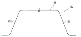
- the line beam laser beam 150 has a flat portion 151 that is 96% or more of the maximum energy intensity, and is located at both ends in the major axis direction and has an energy intensity smaller than that of the flat portion 151. And a steepness portion 152 in which the energy intensity gradually decreases toward the outside.
- the steepness portion is an area in the range of 10% to 90% of the maximum strength.
- the scanning device 3 controlled by the control unit 7 By moving the silicon film 100 b at a predetermined scanning speed by the scanning device 3 controlled by the control unit 7, it is possible to irradiate the semiconductor substrate 100 while scanning the line beam laser light 150 relative to the semiconductor substrate 100. it can.
- the scanning speed at this time is, for example, in the range of 1 to 100 mm / second.
- the scanning speed is not limited to a specific one.
- the scanning pitch is not limited to a specific numerical value, but can be in the range of 5 to 15 ⁇ m, for example.
- the operation of the support unit 4 when the line beam laser beam 150 is irradiated will be described.
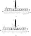
- the semiconductor substrate 100 is moved by moving the scanning direction moving unit 30 by the scanning device 3, and as a result, the line beam laser light 150 is scanned relative to the semiconductor substrate 100. .
- the raising and lowering of the support pins 40 in the support portion 4 is controlled according to the irradiation position of the line beam laser beam 150.
- the support of the support pins 40 corresponding to the partial region 111 of the semiconductor substrate 100 including the irradiation region 110 irradiated with the line beam laser beam 150 is released.
- the line beam laser beam is described as being irradiated.
- the present invention is not limited to the line beam shape of the laser beam irradiated to the object to be processed. It may be laser light on a spot. However, the effect of the present invention becomes more prominent in line beam laser light that irradiates a large area at a time.
- the support pin 40 of P6 corresponding to the partial region 111 is lowered to release the support of the semiconductor substrate 100, and from the lower surface of the semiconductor substrate 100. Leave downwards. Other support pins support the semiconductor substrate 100.
- the range of the partial region 111 can be appropriately set as a range in which the influence of the support is considered to occur when the line beam laser beam 150 is irradiated. It is also possible to limit the partial area 111 to the irradiation area.
- the scanning direction moving unit 30 moves in the relative scanning of the line beam laser beam 150
- the irradiation position of the line beam laser beam 150 with respect to the semiconductor substrate 100 relatively moves, whereby the irradiation region 110 and the partial region 111 are also moved. It moves relative to the semiconductor substrate 100.
- the partial region 111 hits the P7 of the adjacent support pin 40
- the support pin 40 of the P7 is lowered, and the P6 of the partial region 112 that has been released from the support in the irradiated region outside the partial region 111 is released.
- the support pins 40 are raised to support the semiconductor substrate 100 again.
- the support pins 40 along the direction intersecting the scanning direction are moved up and down in synchronization. Further, the support pins 40 along the direction intersecting the scanning direction may be moved up and down at the same time by being connected by a connecting member or the like in addition to moving up and down in synchronization with each other.
- FIG. 2A the example in which the support pins 40 are arranged vertically and horizontally as shown in FIG. 2A has been described.
- a plurality of long fixed cylinders 43 along the direction intersecting the scanning direction of the line beam are arranged so as to be arranged at intervals in the scanning direction, and the long support pieces 42 are arranged on the fixed cylinder 43. Is provided so that it can be raised and lowered.
- the fixed cylinder 43 and the support piece 42 constitute a support part, and the support piece 42 constitutes a movable part.
- the upper part of the support piece 42 constitutes an operating part.
- the semiconductor substrate 100 is supported by the support piece 42.
- the support piece 42 can be moved up and down along the direction intersecting the scanning direction, and a complicated mechanism is used for releasing the support of the support portion and performing the subsequent re-support with the scanning of the line beam-shaped line beam laser beam 150. Can be done without having.
- the support part having the movable part can be moved so that a robot hand for carrying in and out the object to be processed passes through, and does not require a pusher pin used in the past, and eliminates the time for raising and lowering the pusher pin. Productivity can be improved.
- FIG. 5A shows an annealing base of this form
- FIG. 5B shows an enlarged view of the support adsorption cylinder 50 provided on the annealing base.
- the annealing base has support adsorption cylinders 50 arranged vertically and horizontally at predetermined intervals on the scanning direction moving unit 30.
- the support adsorption cylinder 50 constitutes a support part of the present invention.
- a suction line 51 and an open line 53 are connected to a suction hole 50 a configured by a cylindrical hole, a suction pump 52 is connected to the suction line 51, and an open valve 54 is connected to the open line 53. Is connected.
- a negative pressure lower than the atmospheric pressure is generated in the suction hole 50 a of the support suction cylinder 50 through the suction line 51 by the operation of the suction pump 52, so that the back surface of the semiconductor substrate 100 above the support suction cylinder 50 is placed.
- the semiconductor substrate 100 is supported by adsorption.
- the release valve 54 is closed.
- the upper part of the support adsorption cylinder 50 constitutes an adsorption part.
- the operation of the suction pump 52 is stopped and the release valve 54 is opened so that the air flows into the suction hole 50a through the release valve 54 and the release line 53, and is supported by the support suction cylinder 50.
- the adsorption of the semiconductor substrate 100 is released.
- the adsorption and release of adsorption in the support adsorption cylinder 50 are switched according to the irradiation position of the line beam laser beam 150, so that the support adsorption cylinder 50 is located in and around the irradiation region of the line beam laser beam 150 as in the above embodiments. Annealing treatment can be performed so as not to cause the influence of support by the above.
- the adsorption of the support adsorption cylinder 50 corresponding to a partial area of the semiconductor substrate 100 including the irradiation area irradiated with the laser light is released.
- the range of the partial region can be appropriately set as a range that is considered to be affected by the support when the line beam laser beam 150 is irradiated.
- the scanning direction moving unit 30 moves in the relative scanning of the line beam laser beam 150, the irradiation position of the line beam laser beam 150 with respect to the semiconductor substrate 100 relatively moves, whereby the irradiation region and part of the region are also in the semiconductor substrate. Since it moves relative to 100, when a partial area is applied to the adjacent support adsorption cylinder 50, the adsorption of the support adsorption cylinder 50 is released, and the support that has been released from the partial area and has been previously desorbed. The adsorption is started again by the adsorption cylinder 50 and the semiconductor substrate 100 is supported.
- the support by the support adsorption cylinder 50 does not affect the annealing when the line beam laser beam 150 is irradiated. Can do.
- the support adsorption cylinders 50 along the direction intersecting the scanning direction are synchronously adsorbed and desorbed. Further, the support suction cylinder 50 along the direction intersecting the scanning direction is not only suctioned and released from suction in synchronization with each other, but also connected to a suction line and an open line so that suction and suction can be released simultaneously. Good. *
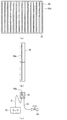
- a plurality of elongate support suction blocks 60 along the intersecting direction can be arranged in a row at a predetermined interval in the scanning direction.
- the support suction block 60 has substantially the same length as the width in the scanning direction crossing direction of the scanning direction moving unit 30, and has a suction groove 60 a on the upper surface along the longitudinal direction of the support suction block 60.
- the suction grooves 60a reach the vicinity of both ends in the longitudinal direction of the support suction block 60 and have a length that does not reach both ends in the longitudinal direction.
- the support suction block 60 has a suction line 61 and an open line 63 connected to the suction groove 60a, a suction pump 62 connected to the suction line 61, and an open valve 64 connected to the open line 63.
- a negative pressure lower than the atmospheric pressure is generated in the suction groove 60 a of the support suction block 60 through the suction line 61 by the operation of the suction pump 62, so that the back surface of the semiconductor substrate 100 above the support suction block 60 is formed.
- the semiconductor substrate 100 is supported by adsorption.
- the release valve 64 is closed.
- the upper part of the support adsorption block 60 constitutes a suction part.
- the operation of the suction pump 62 is stopped and the release valve 64 is opened so that the atmosphere flows into the suction groove 60a through the release valve 64 and the release line 63.
- the adsorption of the semiconductor substrate 100 is released.
- the support adsorption block is used in the irradiation area of the line beam laser beam 150 and its surroundings in the same manner as in the above embodiments. Annealing treatment can be performed so that the influence of support by 60 does not occur.
- the suction of the support suction block 60 corresponding to a partial region of the semiconductor substrate 100 including the irradiation region irradiated with the laser light is released.
- the range of the partial region can be appropriately set as a range that is considered to be affected by the support when the line beam laser beam 150 is irradiated.
- the support adsorption cylinder 50 and the support adsorption block 60 it has been described that the support and the release of the support are performed by the adsorption and the cancellation of the adsorption.
- the support adsorption cylinder 50 and the support suction block 60 may be moved up and down with suction and release of suction. That is, when adsorbing, these members are raised and brought into contact with the back side of the semiconductor substrate or have a very small gap, and when releasing the adsorbing, these members are lowered and the back side of the semiconductor substrate is placed. And a sufficient interval. It should be noted that it is desirable that the height of the surface of the object to be processed does not change when the support part is moved up and down relative to the object to be processed.
- the spacing between the support pins, the support pieces, the support suction cylinders, the support suction blocks, and the like is such that the amount of deflection of the semiconductor substrate partially falls within a predetermined range when the support is released by any member. It is desirable to set The predetermined range of the deflection amount can be determined as appropriate, for example, from the viewpoint that no trouble occurs in the annealing process, or from the viewpoint that it can be handled by adjusting the optical system or the like. Below, the structure which adjusts the irradiation position in the irradiation direction of a laser beam according to the bending etc. of a semiconductor substrate is demonstrated.
- the laser processing apparatus 1 a shown in FIG. 7 includes a processing chamber 2, a scanning device 3, a scanning direction moving unit 30, a support unit 4, and an introduction window 6, similar to the laser processing device 1. Includes a laser light source 10, an optical system 12, and a control unit 7. These configurations are the same as those of the laser processing apparatus 1, and detailed description thereof is omitted here.
- the laser processing apparatus 1 a includes a height measuring device 8 that measures the distance from the surface of the semiconductor substrate 100 at a position on the front side in the scanning direction of the line beam laser beam 150.
- the height measuring device 8 is fixed at a fixed position and can continuously or intermittently measure the surface height of the semiconductor substrate 100 that moves with scanning.
- the height measuring device 8 corresponds to a position detection unit. In the configuration in which the laser beam irradiated to the object to be processed moves, it is desirable to move the height measuring device in the same manner.
- the output of the height measuring device 8 is configured to be sent to the control unit 7, and the control unit 7 can calculate the height amount of the semiconductor substrate 100 based on the measurement result.
- the condenser lens 12 b can be moved along the optical axis direction by a driving device (not shown), and the driving device is controlled by the control unit 7. That is, the irradiation position in the irradiation direction can be adjusted by laser light irradiation corresponding to the measurement position based on the measurement result.
- the adjustment of the irradiation position is performed by adjusting the position of the condenser lens 12b in the optical axis direction so that the focal position becomes a fixed position with respect to the surface of the semiconductor substrate 100.
- the driving device for the condenser lens 12b and the control unit 7 cooperate to constitute an irradiation position adjusting unit.
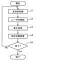
- step s1 the support of the support portion corresponding to the partial region including the irradiation region of the line beam laser beam 150 is released (step s1).
- step s2 laser light is irradiated (step s2)
- step s3 the control unit 7
- the control unit 7 adjusts the condensing lens 12b so that the focal point is fixed with respect to the surface of the semiconductor substrate 100 when the line beam laser beam 150 is irradiated at the measurement position.
- a control signal is sent by the driving device for the condenser lens 12b so as to obtain the adjustment amount, and the irradiation position in the irradiation direction is adjusted (step s4).
- the measurement position is grasped in advance by the control unit 7, and the control unit 7 performs control so that adjustment is performed after a predetermined time in relation to the scanning speed.
- step s5 it is determined whether the process is finished (step s5). If the process is finished (step s5, Yes), the process is finished. If the process is not finished (step s5, No), the process returns to step s1 and the process is continued. . Note that in the case where laser beam irradiation has already been started, in step s1, the support portion that is out of the partial region including the laser beam irradiation region performs a process of supporting the semiconductor substrate again.
- annealing treatment can be performed on a desired surface (for example, the entire surface) of the semiconductor substrate.
- the adjustment of the laser light irradiation position based on the above height measurement can be adjusted according to the bending of the semiconductor substrate, and can also be adjusted in the case where an inclination occurs with the movement of the base.
- Processing can be performed uniformly on the entire processing surface. For example, when a result is obtained as an annealing treatment, a uniform crystal can be obtained.
- the present invention can be suitably used in the field of manufacturing high-performance displays such as OLEDs and high-definition LCDs, and can also meet high requirements for unevenness after irradiation.
- the present invention even if the substrate size is further increased, the overall size of the mounting table and the like is not changed, but it is easy to cope by adding a support portion, and the weight and flatness of the mounting table due to the increase in size are increased. Can solve the problem of degree.
- the present invention has been described based on the above embodiment, but the present invention is not limited to the content of the above embodiment, and can be appropriately changed without departing from the scope of the present invention. .
Landscapes
- Recrystallisation Techniques (AREA)
- Container, Conveyance, Adherence, Positioning, Of Wafer (AREA)
Abstract
Description
このレーザアニール装置では、例えばアニール処理を行う未処理の半導体基板を載置台の上に載置し、レーザ照射部分が半導体基板の照射スタート点に位置するように載置台を移動させる。その後、レーザ光を半導体基板の表面に照射しつつ載置台を移動することでレーザ光を走査する。これにより、半導体基板が結晶化される。
なお、レーザアニール装置では、ロボットのハンドなどで搬送してきた半導体基板を、移動載置台上面から突出作動させたプッシャピンなどの上に支持して水平に受け取り、その後、プッシャピンに没入作動を与えてレーザ照射を行い、処理完了後はプッシャピンを突き出して搬出を行う構成(特許文献2参照)や、載置台上面で半導体基板を吸着して固定する機構(特許文献3参照)などを有するものが知られている。
この穴や溝の上に位置する半導体基板の領域にレーザ光を照射すると、穴や溝が位置していない半導体基板の領域にレーザ光を照射した場合と比較して照射結果が変わり、照射ムラが発生するという問題がある。これは、穴や溝の上に位置する半導体基板にレーザ光を照射した場合と、穴や溝の上に位置していない半導体基板にレーザ光を照射した場合とで、熱効果や光反射効果が異なるためである。
前記被処理体を複数箇所で支持し、前記レーザ光の相対的な走査に伴って、前記レーザ光の照射領域を含む前記被処理体の一部領域に対する支持を順次、解除するとともに、前記照射領域の移動に伴って、前記レーザ光の照射が完了し、前記支持が解除されている一部領域に対し順次、再支持することを特徴とする。
レーザ光を出力するレーザ光源と、
前記レーザ光を導いて前記レーザアニール基台で支持されている被処理体に前記レーザ光を照射する光学系と、
前記レーザ光を前記被処理体に対し相対的に走査する走査装置と、を備えることを特徴とする。
前記制御部は、前記位置検知部による検知結果を受け、該検知結果に応じて、前記照射位置調整部によって前記検知位置に照射される前記レーザ光の前記照射位置を調整することを特徴とする。
レーザ処理装置1は、処理室2を備えており、処理室2内に走査装置3が設けられている。走査装置3はX方向(走査方向)に移動可能な走査方向移動部30を有しており、該走査方向移動部30上に、走査方向移動部30とともに移動する支持部4が設けられている。
走査方向移動部30は、処理室2の基盤上にX方向に伸張して設けられたガイド31に沿って移動可能とされており、図示しないモータなどによって駆動され、支持部4を走査方向に移動させることができる。
上記した走査方向移動部30およびガイド31を備える走査装置3、支持部4は本発明のアニール基台を構成する。
また、処理室2には、外部からラインビームを導入する導入窓6が設けられている。
なお、本実施形態の処理装置は、非晶質膜をレーザ処理により結晶化するレーザアニール処理に関するものとして説明するが、本願発明としてはレーザ処理の内容がこれに限定されるものではなく、例えば、非単結晶の半導体膜を単結晶化したり、結晶半導体膜の改質を行うものであってよい。また、その他の処理に関わるものであってもよく、被処理体が特定のものに限定されるものではない。
該レーザ光源10において出力されるパルス状のレーザ光15は、必要に応じてアテニュエータ11でエネルギー密度が調整され、反射ミラー12a、集光レンズ12b、反射ミラー12cなどを含む光学系12でラインビーム形状などへの整形や偏向などがなされる。なお、光学系12を構成する光学部材は上記に限定されるものではなく、各種レンズ、ミラー、導波部などを備えることができる。
また、本実施形態では、レーザ光15のビーム断面形状はラインビーム形状であるものとして説明するが、本発明としてはこれに限定されるものではなく、スポット状、円形状、長方形状など、適宜の形状とすることができる。
支持部4は、図2(a)に示すように、走査方向移動部30上に互いに間隔を置いて縦横に設置された固定筒41に支持ピン40が昇降可能に設けられた構成を有しており、各支持ピン40は、互いに独立して昇降が可能になっている。支持ピン40は、可動部に相当する。また、支持ピン40の上部は、作用部に相当する。
各支持ピン40の昇降は、図示しない駆動装置に行われ、該昇降は制御部7によって制御される。制御部7では、レーザ光15の照射位置に同期させて、各支持ピン40の昇降を行うことができる。なお、上記駆動装置は、例えば走査方向移動部30などに設けることができる。
パルス発振レーザ光源10において、制御部7の制御によって所定の繰り返し周波数でパルス発振されて、所定出力でレーザ光15が出力される。レーザ光15は、例えば、波長400nm以下、パルス半値幅が200n秒以下のものが例示される。ただし、本発明としてはこれらに限定されるものではない。
レーザ光15は、制御部7により制御されるアテニュエータ11でパルスエネルギー密度が調整される。アテニュエータ11は所定の減衰率に設定されており、シリコン膜100bへの照射面上で結晶化に最適な照射パルスエネルギー密度が得られるように、減衰率が調整される。例えば非晶質のシリコン膜100bを結晶化するなどの場合、その照射面上において、エネルギー密度が250~500mJ/cm2となるように調整することができる。
ラインビームは、例えば、長軸側の長さが370~1300mm、短軸側の長さが100μm~500μmのものに整形される。
走査ピッチは、特定の数値に限定されるものではないが、例えば5~15μmの範囲を挙げることができる。
上記したように、レーザ処理に際しては、走査装置3によって走査方向移動部30が移動することで半導体基板100が移動し、結果としてラインビームレーザ光150が半導体基板100に対し相対的に走査される。この際に、ラインビームレーザ光150の照射位置に従って、支持部4における支持ピン40の昇降が制御される。具体的には、ラインビームレーザ光150が照射されている照射領域110を含む半導体基板100の一部領域111に対応する支持ピン40の支持が解除される。なお、この実施形態では、ラインビームレーザ光を照射するものとして説明しているが、本願発明としては被処理体に照射されるレーザ光のビーム形状がラインビームに限定されるものではなく、例えばスポット上のレーザ光などであってもよい。ただし、一度に広い面積を照射するラインビームレーザ光において本願発明の効果はより顕著になる。
半導体基板100は、支持片42で支持される。この支持片42は、走査方向と交差する方向に沿って昇降することができ、ラインビーム形状のラインビームレーザ光150の走査に伴って支持部の支持解除、その後の再支持を複雑な機構を有することなく行うことができる。
上記可動部を有する支持部は、被処理体の搬入及び搬出のためのロボットのハンドが通るように可動することができ、従来用いられているプッシャピンを不要にし、また、プッシャピンの上げ下げ時間をなくすことで生産性を向上させることができる。
図5(a)にこの形態のアニール基台を示し、図5(b)に、アニール基台に設けられた支持吸着筒50を拡大して示す。
アニール基台では、走査方向移動部30上に、所定の間隔で縦横に配置される支持吸着筒50を有している。支持吸着筒50は、本発明の支持部を構成する。支持吸着筒50は、筒穴で構成された吸着穴50aに吸引ライン51と開放ライン53とが接続されており、吸引ライン51には吸引ポンプ52が接続され、開放ライン53には開放弁54が接続されている。各支持吸着筒50では、吸引ポンプ52の動作によって吸引ライン51を通して支持吸着筒50の吸着穴50a内に大気圧よりも低い負圧を生じさせて支持吸着筒50上方の半導体基板100の裏面を吸着して半導体基板100を支持する。この際には開放弁54は閉じておく。支持吸着筒50の上部は吸着部を構成する。
支持吸着筒50における吸着および吸着の解除は、ラインビームレーザ光150の照射位置に応じて切り替えることで、前記各実施形態と同様にラインビームレーザ光150の照射領域とその周辺で支持吸着筒50による支持の影響が生じないようにしてアニール処理を行うことができる。
具体的には、レーザ光が照射されている照射領域を含む半導体基板100の一部領域に対応する支持吸着筒50の吸着が解除される。なお、一部領域の範囲は、ラインビームレーザ光150が照射された際に、支持による影響が生じると考えられる範囲を適宜設定することができる。
支持吸着ブロック60は、走査方向移動部30の走査方向交差方向幅と略同じ長さを有し、上面には、支持吸着ブロック60の長尺方向に沿って吸着溝60aを有している。吸着溝60aは、支持吸着ブロック60の長尺方向両端付近に至り、長尺方向両端には至らない長さを有している。
支持吸着ブロック60における吸着と吸着の解除とを、ラインビームレーザ光150の照射位置に応じて切り替えることで、前記各実施形態と同様にラインビームレーザ光150の照射領域とその周辺で支持吸着ブロック60による支持の影響が生じないようにアニール処理を行うことができる。
具体的には、レーザ光が照射されている照射領域を含む半導体基板100の一部領域に対応する支持吸着ブロック60の吸着が解除される。なお、一部領域の範囲は、ラインビームレーザ光150が照射された際に、支持による影響が生じると考えられる範囲を適宜設定することができる。
なお、被処理体に対する支持部の昇降では、昇降に際し被処理体の表面の高さの変化が起きないようにするのが望ましい。
高さ測定器8の出力は、制御部7に送出されるように構成されており、制御部7では、測定結果を受けて半導体基板100の高さ量を算出することができる。また、光学系12では、集光レンズ12bが図示しない駆動装置によって光軸方向に沿って移動可能になっており、その駆動装置は制御部7によって制御される。すなわち、測定結果に基づいて測定位置に対応するレーザ光照射で照射方向における照射位置を調整することができる。照射位置の調整は、集光レンズ12bの光軸方向における位置を調整して焦点位置が半導体基板100の表面に対し一定の位置になるようにすることで行う。上記集光レンズ12bの駆動装置と制御部7とは協働して照射位置調整部を構成する。
処理開始に伴って、ラインビームレーザ光150の照射領域を含む一部領域に対応する支持部の支持を解除する(ステップs1)。次いでレーザ光を照射し(ステップs2)、照射位置の走査方向前方で半導体基板100の表面高さを高さ測定器8で測定し、測定結果を制御部7に送出する(ステップs3)。測定結果を受けた制御部7では、測定位置においてラインビームレーザ光150が照射される際に、その焦点が半導体基板100の表面に対し一定の位置になるように、集光レンズ12bの調整量を算出し、該調整量が得られるように集光レンズ12bに対する駆動装置で制御信号を送出し、照射方向における照射位置を調整する(ステップs4)。なお、測定位置は、予め制御部7で把握されており、制御部7は、走査速度との関係で所定の時間後に調整がなされるように制御する。
本発明は、OLEDや高精細LCDなどの高性能のディスプレイの製造分野に好適に使用することができ、照射後のムラに対する高い要求仕様にも対応することができる。
また、本発明では、基板サイズがさらに大型化されても載置台など全体のサイズを変えるのではなく、支持部を追加することにより、対応が容易であり、大型化による載置台の重さや平坦度の問題を解決することができる。
1a レーザ処理装置
2 処理室
3 走査装置
4 支持部
6 挿入窓
7 制御部
10 レーザ光源
12 光学系
12b 集光レンズ
40 支持ピン
42 支持片
50 支持吸着筒
60 支持吸着ブロック
100 半導体基板
Claims (15)
- 被処理体にレーザ光を相対的に走査しつつ照射して前記被処理体のアニールを行うアニール被処理体の製造方法において、
前記被処理体を複数箇所で支持し、前記レーザ光の相対的な走査に伴って、前記レーザ光の照射領域を含む前記被処理体の一部領域に対する支持を順次、解除するとともに、前記照射領域の移動に伴って、前記レーザ光の照射が完了し、前記支持が解除されている一部領域に対し順次、再支持することを特徴とするアニール被処理体の製造方法。 - 前記支持の解除では、前記一部領域から前記支持の作用部を前記被処理体から離脱させることを特徴とする請求項1記載のアニール被処理体の製造方法。
- 前記被処理体が非単結晶半導体基板であることを特徴とする請求項1または2に記載のアニール被処理体の製造方法。
- 前記非単結晶半導体基板が非単結晶シリコン基板であることを特徴とする請求項3記載のアニール被処理体の製造方法。
- 前記レーザ光がパルスレーザ光であり、前記走査方向のビーム断面形状に強度の均一な平坦部を有することを特徴とする請求項1~4のいずれかに記載のアニール被処理体の製造方法。
- 前記レーザ光の照射の際に、前記照射領域の走査方向前方側で前記支持が解除されている前記一部領域内において、前記レーザ光の照射方向における前記被処理体の位置を検知し、該検知の結果に基づいて、検知位置に対する、前記レーザ光の照射方向における前記レーザ光の照射位置を調整することを特徴とする請求項1~5のいずれかに記載のアニール被処理体の製造方法。
- レーザ光が相対的に走査されつつ上面側から照射される被処理体を前記被処理体の下面側の複数箇所で支持する複数の支持部を備え、
前記複数の支持部は、前記レーザ光を相対的な走査をしつつ照射している際に、それぞれが個別に前記支持と前記支持の解除の切り替え動作が可能に構成されていることを特徴とするレーザアニール基台。 - 前記支持部が上下方向に移動可能な可動部を有しており、前記被処理体の支持に際し前記可動部が上昇し、前記被処理体に対する支持の解除に際し前記可動部が下降するように構成されていることを特徴とする請求項7に記載のレーザアニール基台。
- 前記支持部が上端に吸引部を有しており、前記被処理体の支持に際し前記吸引部の吸引によって前記被処理体に吸着し、前記被処理体に対する支持の解除に際し前記吸引部の吸引停止を行うように構成されていることを特徴とする請求項7または8に記載のレーザアニール基台。
- 前記支持部の切り替え動作を制御する制御部を備え、該制御部は、前記被処理体の面方向における前記レーザ光の照射位置に応じて、前記支持部の前記支持と前記支持解除の切り替え動作を制御することを特徴とする請求項7~9のいずれかに記載のレーザアニール基台。
- 前記制御部は、前記レーザ光が相対的に走査されつつ照射されるのに従って、前記レーザ光が照射されている照射領域を含む前記半導体基板の一部領域を支持している前記支持部の支持を順次、解除するとともに、前記レーザ光の照射が完了した照射済み領域を含み、前記支持が解除されている一部領域に対し前記支持部による支持を順次、行うように切り替え制御することを特徴とする請求項10記載のレーザアニール基台。
- 請求項7~9のいずれかに記載のレーザアニール基台と、
レーザ光を出力するレーザ光源と、
前記レーザ光を導いて前記レーザアニール基台で支持されている被処理体に前記レーザ光を照射する光学系と、
前記レーザ光を前記被処理体に対し相対的に走査する走査装置と、を備えることを特徴とするレーザアニール処理装置。 - 前記走査装置の走査動作と、前記支持部の切り替え動作とを制御する制御部を備えることを特徴とする請求項12記載のレーザアニール処理装置。
- 前記レーザ光が照射されている際に、被処理体の照射領域の走査方向前方でレーザ光照射方向における被処理体の位置を検知する位置検知部と、前記レーザ光におけるレーザ光照射方向における照射位置を調整する照射位置調整部とを備え、
前記制御部は、前記位置検知部による検知結果を受け、該検知結果に応じて、前記照射位置調整部によって前記検知位置に照射される前記レーザ光の前記照射位置を調整することを特徴とする請求項13記載のレーザアニール処理装置。 - 前記照射位置調整部が、前記光学系において前記レーザ光の焦点位置を調整する機構を有することを特徴とする請求項14記載のレーザアニール処理装置。
Priority Applications (2)
| Application Number | Priority Date | Filing Date | Title |
|---|---|---|---|
| KR1020147033513A KR101583535B1 (ko) | 2013-03-26 | 2014-02-19 | 어닐 피처리체의 제조 방법, 레이저 어닐 지지대 및 레이저 어닐 처리 장치 |
| CN201480001793.7A CN104412366B (zh) | 2013-03-26 | 2014-02-19 | 退火被处理体的制造方法、激光退火基台及激光退火处理装置 |
Applications Claiming Priority (2)
| Application Number | Priority Date | Filing Date | Title |
|---|---|---|---|
| JP2013065173A JP5858438B2 (ja) | 2013-03-26 | 2013-03-26 | アニール被処理体の製造方法、レーザアニール基台およびレーザアニール装置 |
| JP2013-065173 | 2013-03-26 |
Publications (1)
| Publication Number | Publication Date |
|---|---|
| WO2014156380A1 true WO2014156380A1 (ja) | 2014-10-02 |
Family
ID=51623381
Family Applications (1)
| Application Number | Title | Priority Date | Filing Date |
|---|---|---|---|
| PCT/JP2014/053936 Ceased WO2014156380A1 (ja) | 2013-03-26 | 2014-02-19 | アニール被処理体の製造方法、レーザアニール基台およびレーザアニール処理装置 |
Country Status (4)
| Country | Link |
|---|---|
| JP (1) | JP5858438B2 (ja) |
| KR (1) | KR101583535B1 (ja) |
| CN (1) | CN104412366B (ja) |
| WO (1) | WO2014156380A1 (ja) |
Cited By (2)
| Publication number | Priority date | Publication date | Assignee | Title |
|---|---|---|---|---|
| US20190255650A1 (en) * | 2016-10-20 | 2019-08-22 | The Japan Steel Works, Ltd. | Annealed workpiece manufacturing method, laser anneal base stage, and laser anneal processing apparatus |
| US11264259B2 (en) | 2015-10-27 | 2022-03-01 | The Japan Steel Works, Ltd. | Workpiece conveyance apparatus, semiconductor manufacturing apparatus, and workpiece conveyance method |
Families Citing this family (4)
| Publication number | Priority date | Publication date | Assignee | Title |
|---|---|---|---|---|
| JP6829118B2 (ja) * | 2017-03-16 | 2021-02-10 | 株式会社日本製鋼所 | レーザ照射装置、レーザ照射方法、及び半導体装置の製造方法 |
| CN109887876B (zh) * | 2017-12-06 | 2020-02-21 | 上海微电子装备(集团)股份有限公司 | 真空吸盘、基底吸附方法、激光退火装置和方法 |
| CN108226166A (zh) * | 2017-12-29 | 2018-06-29 | 信利(惠州)智能显示有限公司 | 一种自动光学检测扫描方法 |
| JP7336369B2 (ja) * | 2019-11-25 | 2023-08-31 | 株式会社Screenホールディングス | 基板支持装置、熱処理装置、基板支持方法、熱処理方法 |
Citations (6)
| Publication number | Priority date | Publication date | Assignee | Title |
|---|---|---|---|---|
| JPS6390386A (ja) * | 1986-10-02 | 1988-04-21 | Mitsubishi Electric Corp | レ−ザ−加工用被加工物固定装置 |
| JP2004247340A (ja) * | 2003-02-10 | 2004-09-02 | Dainippon Screen Mfg Co Ltd | 熱処理装置および熱処理方法 |
| JP2005197548A (ja) * | 2004-01-09 | 2005-07-21 | Japan Steel Works Ltd:The | 基板の位置決め方法及びその装置 |
| JP2008210965A (ja) * | 2007-02-26 | 2008-09-11 | Sumitomo Heavy Ind Ltd | 基板保持装置及びレーザアニール装置 |
| JP2009010161A (ja) * | 2007-06-28 | 2009-01-15 | Sumitomo Heavy Ind Ltd | レーザ加工装置、及び、レーザ加工方法 |
| JP2009252796A (ja) * | 2008-04-01 | 2009-10-29 | Semiconductor Energy Lab Co Ltd | 半導体装置及びその作製方法 |
Family Cites Families (4)
| Publication number | Priority date | Publication date | Assignee | Title |
|---|---|---|---|---|
| JPH10135149A (ja) | 1996-11-01 | 1998-05-22 | Japan Steel Works Ltd:The | レーザーアニール処理装置 |
| JP2005019914A (ja) | 2003-06-30 | 2005-01-20 | Japan Steel Works Ltd:The | 基板の授受装置 |
| JP2007331031A (ja) | 2006-06-12 | 2007-12-27 | Japan Steel Works Ltd:The | ワーク支持装置 |
| JP2008016543A (ja) * | 2006-07-04 | 2008-01-24 | Dainippon Screen Mfg Co Ltd | 基板処理装置 |
-
2013
- 2013-03-26 JP JP2013065173A patent/JP5858438B2/ja active Active
-
2014
- 2014-02-19 WO PCT/JP2014/053936 patent/WO2014156380A1/ja not_active Ceased
- 2014-02-19 CN CN201480001793.7A patent/CN104412366B/zh active Active
- 2014-02-19 KR KR1020147033513A patent/KR101583535B1/ko active Active
Patent Citations (6)
| Publication number | Priority date | Publication date | Assignee | Title |
|---|---|---|---|---|
| JPS6390386A (ja) * | 1986-10-02 | 1988-04-21 | Mitsubishi Electric Corp | レ−ザ−加工用被加工物固定装置 |
| JP2004247340A (ja) * | 2003-02-10 | 2004-09-02 | Dainippon Screen Mfg Co Ltd | 熱処理装置および熱処理方法 |
| JP2005197548A (ja) * | 2004-01-09 | 2005-07-21 | Japan Steel Works Ltd:The | 基板の位置決め方法及びその装置 |
| JP2008210965A (ja) * | 2007-02-26 | 2008-09-11 | Sumitomo Heavy Ind Ltd | 基板保持装置及びレーザアニール装置 |
| JP2009010161A (ja) * | 2007-06-28 | 2009-01-15 | Sumitomo Heavy Ind Ltd | レーザ加工装置、及び、レーザ加工方法 |
| JP2009252796A (ja) * | 2008-04-01 | 2009-10-29 | Semiconductor Energy Lab Co Ltd | 半導体装置及びその作製方法 |
Cited By (3)
| Publication number | Priority date | Publication date | Assignee | Title |
|---|---|---|---|---|
| US11264259B2 (en) | 2015-10-27 | 2022-03-01 | The Japan Steel Works, Ltd. | Workpiece conveyance apparatus, semiconductor manufacturing apparatus, and workpiece conveyance method |
| US20190255650A1 (en) * | 2016-10-20 | 2019-08-22 | The Japan Steel Works, Ltd. | Annealed workpiece manufacturing method, laser anneal base stage, and laser anneal processing apparatus |
| US11938563B2 (en) * | 2016-10-20 | 2024-03-26 | Jsw Aktina System Co., Ltd. | Annealed workpiece manufacturing method, laser anneal base stage, and laser anneal processing apparatus |
Also Published As
| Publication number | Publication date |
|---|---|
| CN104412366B (zh) | 2016-04-27 |
| JP5858438B2 (ja) | 2016-02-10 |
| CN104412366A (zh) | 2015-03-11 |
| JP2014192267A (ja) | 2014-10-06 |
| KR101583535B1 (ko) | 2016-01-08 |
| KR20140143852A (ko) | 2014-12-17 |
Similar Documents
| Publication | Publication Date | Title |
|---|---|---|
| JP5858438B2 (ja) | アニール被処理体の製造方法、レーザアニール基台およびレーザアニール装置 | |
| US9610653B2 (en) | Method and apparatus for separation of workpieces and articles produced thereby | |
| KR100297314B1 (ko) | 반도체디바이스의레이저처리방법 | |
| TWI508144B (zh) | 雷射回火處理裝置以及雷射回火處理方法 | |
| CN108352347B (zh) | 被处理体搬送装置、半导体制造装置及被处理体搬送方法 | |
| JP2012508985A (ja) | 薄膜の結晶化のためのシステムおよび方法 | |
| CN109863577B (zh) | 退火被处理体的制造方法、激光退火基台和激光退火处理装置 | |
| KR102189427B1 (ko) | 어닐 처리 반도체 기판의 제조 방법, 주사 장치 및 레이저 처리 장치 | |
| WO2010001727A1 (ja) | レーザアニール装置 | |
| JP2002280321A (ja) | レーザアニール装置 | |
| WO2011142154A1 (ja) | レーザアニール処理装置、レーザアニール処理体の製造方法およびレーザアニール処理プログラム | |
| JP2021015931A (ja) | 基板浮上型レーザ処理装置及び浮上量の測定方法 | |
| TWI633589B (zh) | 一種雷射退火裝置及雷射退火方法 | |
| JPH0888196A (ja) | レーザー処理方法 | |
| CN104821278A (zh) | 低温多晶硅的制造方法及装置、多晶硅 | |
| JPH11340160A (ja) | レーザアニーリング装置及び方法 | |
| KR102238080B1 (ko) | 레이저 어닐 장치 및 방법 | |
| JP7058907B2 (ja) | 加熱処理装置、アニール装置及び加熱処理方法 | |
| JP3413484B2 (ja) | レーザアニーリング装置 | |
| JP2008153261A (ja) | レーザアニール装置 | |
| JP4946093B2 (ja) | レーザアニール装置のレーザ光のエネルギー決定方法、レーザアニール装置のレーザ光のエネルギー決定装置及びレーザアニール装置及び薄膜トランジスタの製造方法 | |
| JP2004303792A (ja) | フラッシュランプの照射装置 | |
| KR100316272B1 (ko) | 레이저 어닐링 장비 | |
| JP4094093B2 (ja) | レーザアニール装置 | |
| JP2010194594A (ja) | マーキング方法及びマーキング装置 |
Legal Events
| Date | Code | Title | Description |
|---|---|---|---|
| WWE | Wipo information: entry into national phase |
Ref document number: 201480001793.7 Country of ref document: CN |
|
| 121 | Ep: the epo has been informed by wipo that ep was designated in this application |
Ref document number: 14773462 Country of ref document: EP Kind code of ref document: A1 |
|
| ENP | Entry into the national phase |
Ref document number: 20147033513 Country of ref document: KR Kind code of ref document: A |
|
| NENP | Non-entry into the national phase |
Ref country code: DE |
|
| 122 | Ep: pct application non-entry in european phase |
Ref document number: 14773462 Country of ref document: EP Kind code of ref document: A1 |