WO2014156364A1 - タッチパネル及び表示装置 - Google Patents
タッチパネル及び表示装置 Download PDFInfo
- Publication number
- WO2014156364A1 WO2014156364A1 PCT/JP2014/053585 JP2014053585W WO2014156364A1 WO 2014156364 A1 WO2014156364 A1 WO 2014156364A1 JP 2014053585 W JP2014053585 W JP 2014053585W WO 2014156364 A1 WO2014156364 A1 WO 2014156364A1
- Authority
- WO
- WIPO (PCT)
- Prior art keywords
- touch panel
- electrode
- meth
- less
- acrylate
- Prior art date
- Legal status (The legal status is an assumption and is not a legal conclusion. Google has not performed a legal analysis and makes no representation as to the accuracy of the status listed.)
- Ceased
Links
Images




Classifications
-
- G—PHYSICS
- G06—COMPUTING OR CALCULATING; COUNTING
- G06F—ELECTRIC DIGITAL DATA PROCESSING
- G06F3/00—Input arrangements for transferring data to be processed into a form capable of being handled by the computer; Output arrangements for transferring data from processing unit to output unit, e.g. interface arrangements
- G06F3/01—Input arrangements or combined input and output arrangements for interaction between user and computer
- G06F3/03—Arrangements for converting the position or the displacement of a member into a coded form
- G06F3/041—Digitisers, e.g. for touch screens or touch pads, characterised by the transducing means
- G06F3/044—Digitisers, e.g. for touch screens or touch pads, characterised by the transducing means by capacitive means
- G06F3/0446—Digitisers, e.g. for touch screens or touch pads, characterised by the transducing means by capacitive means using a grid-like structure of electrodes in at least two directions, e.g. using row and column electrodes
-
- G—PHYSICS
- G06—COMPUTING OR CALCULATING; COUNTING
- G06F—ELECTRIC DIGITAL DATA PROCESSING
- G06F3/00—Input arrangements for transferring data to be processed into a form capable of being handled by the computer; Output arrangements for transferring data from processing unit to output unit, e.g. interface arrangements
- G06F3/01—Input arrangements or combined input and output arrangements for interaction between user and computer
- G06F3/03—Arrangements for converting the position or the displacement of a member into a coded form
- G06F3/041—Digitisers, e.g. for touch screens or touch pads, characterised by the transducing means
-
- G—PHYSICS
- G06—COMPUTING OR CALCULATING; COUNTING
- G06F—ELECTRIC DIGITAL DATA PROCESSING
- G06F3/00—Input arrangements for transferring data to be processed into a form capable of being handled by the computer; Output arrangements for transferring data from processing unit to output unit, e.g. interface arrangements
- G06F3/01—Input arrangements or combined input and output arrangements for interaction between user and computer
- G06F3/03—Arrangements for converting the position or the displacement of a member into a coded form
- G06F3/041—Digitisers, e.g. for touch screens or touch pads, characterised by the transducing means
- G06F3/0412—Digitisers structurally integrated in a display
-
- G—PHYSICS
- G06—COMPUTING OR CALCULATING; COUNTING
- G06F—ELECTRIC DIGITAL DATA PROCESSING
- G06F3/00—Input arrangements for transferring data to be processed into a form capable of being handled by the computer; Output arrangements for transferring data from processing unit to output unit, e.g. interface arrangements
- G06F3/01—Input arrangements or combined input and output arrangements for interaction between user and computer
- G06F3/03—Arrangements for converting the position or the displacement of a member into a coded form
- G06F3/041—Digitisers, e.g. for touch screens or touch pads, characterised by the transducing means
- G06F3/044—Digitisers, e.g. for touch screens or touch pads, characterised by the transducing means by capacitive means
- G06F3/0445—Digitisers, e.g. for touch screens or touch pads, characterised by the transducing means by capacitive means using two or more layers of sensing electrodes, e.g. using two layers of electrodes separated by a dielectric layer
-
- G—PHYSICS
- G06—COMPUTING OR CALCULATING; COUNTING
- G06F—ELECTRIC DIGITAL DATA PROCESSING
- G06F3/00—Input arrangements for transferring data to be processed into a form capable of being handled by the computer; Output arrangements for transferring data from processing unit to output unit, e.g. interface arrangements
- G06F3/01—Input arrangements or combined input and output arrangements for interaction between user and computer
- G06F3/03—Arrangements for converting the position or the displacement of a member into a coded form
- G06F3/041—Digitisers, e.g. for touch screens or touch pads, characterised by the transducing means
- G06F3/047—Digitisers, e.g. for touch screens or touch pads, characterised by the transducing means using sets of wires, e.g. crossed wires
-
- G—PHYSICS
- G06—COMPUTING OR CALCULATING; COUNTING
- G06F—ELECTRIC DIGITAL DATA PROCESSING
- G06F2203/00—Indexing scheme relating to G06F3/00 - G06F3/048
- G06F2203/041—Indexing scheme relating to G06F3/041 - G06F3/045
- G06F2203/04103—Manufacturing, i.e. details related to manufacturing processes specially suited for touch sensitive devices
-
- G—PHYSICS
- G06—COMPUTING OR CALCULATING; COUNTING
- G06F—ELECTRIC DIGITAL DATA PROCESSING
- G06F2203/00—Indexing scheme relating to G06F3/00 - G06F3/048
- G06F2203/041—Indexing scheme relating to G06F3/041 - G06F3/045
- G06F2203/04112—Electrode mesh in capacitive digitiser: electrode for touch sensing is formed of a mesh of very fine, normally metallic, interconnected lines that are almost invisible to see. This provides a quite large but transparent electrode surface, without need for ITO or similar transparent conductive material
Definitions
- the present invention relates to a touch panel and a display device, and more particularly, to a touch panel and a display device including electrodes including cells having a parallelogram shape by crossing thin silver wires.
- the touch panel includes a sensor for detecting the pressed position when the surface is pressed from an object (for example, a finger).
- the sensor includes a first electrode and a second electrode that extend in directions orthogonal to each other.
- an insulating layer is interposed between the first electrode and the second electrode.
- the first electrode and the second electrode are made of a mesh formed by intersecting thin metal wires so as to be orthogonal to each other (refer to Japanese Unexamined Patent Publication No. 2011-517355).
- the space surrounded by the intersecting fine metal wires is also called a cell. Since the fine metal wires intersect so as to be orthogonal to each other, the cell has a square shape.
- a silver (Ag) fine wire is frequently used from the balance of electrical conductivity, cost, color, and the like.
- the first electrode layer including the first electrode configured as described above or the second electrode layer including the second electrode is formed by an optical adhesive (OCA) as described in JP2011-074308A. Affixed to a display device, a substrate, an optical sheet, or the like. Since the first electrode layer or the second electrode layer is convex with respect to the insulating layer as the base material, a step is formed between the insulating layer and the first electrode layer or the second electrode layer. The OCA is required to be able to satisfactorily cover both the insulating layer and the first electrode layer or the second electrode layer regardless of the step (good step following ability).
- OCA optical adhesive
- the main object of the present invention is to provide a touch panel that employs OCA that has a good penetration into the acute angle portion of the cell, and can avoid the occurrence of ion migration in the silver thin wire.
- Another object of the present invention is to provide a display device having the above touch panel.
- a touch panel having a first electrode layer and a second electrode layer facing each other through an insulating layer
- first electrode layer a plurality of first electrodes extending along a first direction are juxtaposed along a second direction orthogonal to the first direction
- second electrode layer a plurality of second electrodes extending along the second direction are juxtaposed along the first direction
- At least one of the first electrode and the second electrode is made of a mesh formed of silver thin wires having a width direction dimension of 4 ⁇ m or less
- the mesh includes a plurality of cells formed by crossing the silver thin wires, At least one of the cells has a parallelogram shape having an obtuse angle and an acute angle formed by the intersection of the silver thin wires, and an acute angle
- At least one of the first electrode and the second electrode made of the mesh and the insulating layer have a loss coefficient tan ⁇ at 140 ° C. and 1 Hz of 0.13 or more, and a storage elasticity at 25 ° C. and 1 Hz.
- an adhesive having predetermined physical properties is adopted. Since this OCA is excellent in penetration into an acute angle portion and the cell forms a parallelogram having an acute angle, the electrode is satisfactorily covered. Therefore, a gap is hardly generated between the electrode and the OCA. Therefore, it can be avoided that moisture enters between the two. For this reason, it can prevent that the silver which makes a silver thin wire raise
- the resistance value of the silver fine wire tends to change significantly due to ion migration. According to the above, even when the electrode is formed with such an extra fine wire, it is possible to prevent the resistance value of the electrode from changing.
- intersection angle between the silver thin wires is 70 ° or less in the acute diagonal in the cell having the parallelogram shape.
- the cell which makes a parallelogram shape is a rhombus shape.
- the interval between adjacent cells in other words, the cell pitch is 300 ⁇ m or less.
- the width direction dimension of the silver thin wire is preferably 2 ⁇ m or less.
- the pressure-sensitive adhesive include those containing the components shown in the following (A) to (C).
- the adhesive may contain a migration inhibitor composed of a phenolic compound.
- An electrode made of a mesh in the first electrode or the second electrode can be formed by a microcontact printing patterning method or a silver salt method.
- the present invention is a display device including the touch panel described above.
- the touch panel since an adhesive having a predetermined physical property is used, in the touch panel, it is possible to avoid occurrence of ion migration in silver of a silver fine wire forming an electrode having excellent visibility. It is possible to provide a touch panel that can suppress a change in resistance value and that has excellent visibility.
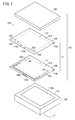
- FIG. 1 is an exploded perspective view of a main part of the touch panel according to the present embodiment.
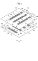
- FIG. 2 is an exploded perspective view of a main part of the laminated conductive sheet constituting the touch panel.
- FIG. 3 is a schematic longitudinal sectional view of the laminated conductive sheet.
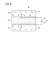
- FIG. 4 is a schematic plan view showing cells of the first electrode formed on the laminated conductive sheet.
- FIG. 5 is a schematic longitudinal sectional view of a laminated conductive sheet according to another embodiment different from FIG.
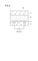
- FIG. 6 is a schematic longitudinal sectional view of a V-mode evaluation base material.
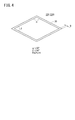
- FIG. 7 is a schematic plan view of a V-mode evaluation base material.
- FIG. 8 is a schematic plan view of an H-mode evaluation base material.
- FIG. 9 is a schematic longitudinal cross-sectional view of an H-mode evaluation base material.
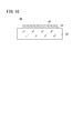
- FIG. 10 is a schematic side view of a base material for a whitening evaluation test.
- FIG. 1 is an exploded perspective view of a main part of a touch panel 100 according to the present embodiment.
- the touch panel 100 includes a sensor body 102 and a control circuit (IC circuit or the like) (not shown).
- the sensor body 102 includes a laminated conductive sheet 12 formed by laminating the first conductive sheet 10A and the second conductive sheet 10B, and a protective layer 106 laminated on the first conductive sheet 10A.
- the sensor main body 102 (the laminated conductive sheet 12 and the protective layer 106) is disposed on the display panel 110 in the display device 108 such as a liquid crystal display, for example.
- the sensor main body 102 includes a sensor unit 112 at a touch position arranged in a region corresponding to the display screen 110 a of the display panel 110 and a terminal arranged in a region corresponding to the outer peripheral portion of the display panel 110.
- a wiring portion 114 (so-called frame).
- the laminated conductive sheet 12 is configured by laminating a first conductive sheet 10A and a second conductive sheet 10B as shown in FIG.
- the first conductive sheet 10A has a first conductive portion 16A as a first electrode layer formed on one main surface of the first transparent base 14A (see FIG. 3), which is an insulating layer.
- a second conductive portion 16B (second) formed on one main surface of the second transparent base 14B (see FIG. 3), which is an insulating layer. Electrode layer).
- the thickness of the first transparent substrate 14A and the second transparent substrate 14B is preferably 50 to 350 ⁇ m or less, more preferably 80 to 250 ⁇ m, and particularly preferably 100 to 200 ⁇ m.
- Examples of the first transparent substrate 14A and the second transparent substrate 14B include a plastic film, a plastic plate, and a glass plate.
- polyesters such as polyethylene terephthalate (PET) and polyethylene naphthalate (PEN); polyolefins such as polyethylene (PE), polypropylene (PP), polystyrene, and EVA; Resin;
- polycarbonate (PC) polyamide, polyimide, acrylic resin, triacetyl cellulose (TAC) and the like can be used.
- PET melting point: 258 ° C.
- PEN melting point: 269 ° C.
- PE melting point: 135 ° C.
- PP melting point: 163 ° C.
- polystyrene melting point: 230 ° C.
- polyvinyl chloride melting point: 180 ° C.
- polyvinylidene chloride melting point: 212 ° C.
- TAC melting point: 290 ° C.
- PET is preferable from the viewpoints of light transmittance and processability. Since the conductive films such as the first conductive sheet 10A and the second conductive sheet 10B used for the laminated conductive sheet 12 are required to be transparent, the transparency of the first transparent base 14A and the second transparent base 14B is high. Is preferred.
- one first conductive portion 16A has a plurality of strip-shaped first conductive patterns 18A (first electrodes) each extending in the first direction (x direction).
- the plurality of first conductive patterns 18A are arranged along a second direction (direction orthogonal to the first direction: y direction).
- Each of the first conductive patterns 18A is formed by the silver thin wires 20 intersecting each other. Along with this intersection, a space (opening) surrounded by the thin silver wire 20, that is, a cell 22A is formed.
- At least one of the cells 22A has a parallelogram shape as shown in FIG. 4, but preferably has a rhombus shape in which the lengths of the four sides are equal.
- the width direction dimension (line width) W of the silver thin wire 20 is 4 ⁇ m or less, and more preferably 2 ⁇ m or less. Thereby, the moire of the conductive pattern by the silver thin wire 20 and the silver thin wire appearance are improved, and the visibility is improved.
- the width direction dimension W of the silver fine wire 20 is 0.5 micrometer or more.
- the rhombus cell 22A shown in FIG. 4 has two obtuse angles and two acute angles.
- the obtuse crossing angle ⁇ in a diagonal relationship is the same angle exceeding 90 °
- the acute crossing angle ⁇ is the same angle less than 90 °.
- the acute angle ⁇ is preferably 70 ° or less. In this case, it is effective in reducing moire. However, moire tends to occur even when ⁇ is excessively small. In order to avoid this, ⁇ is preferably in the range of 30 ° to 70 °, more preferably in the range of 45 ° to 70 °.
- the distance between adjacent cells 22A is preferably 300 ⁇ m or less. This case is also effective in reducing the appearance of moire and silver thin lines.
- each first conductive pattern 18A is electrically connected to a first terminal wiring pattern 42a formed by silver thin wires 20 via a first connection portion 40a.
- the second conductive portions 16B formed on one main surface of the second transparent substrate 14B (see FIG. 3) constituting the second conductive sheet 10B are each in the second direction (y direction) as shown in FIG. ) Extending in a plurality of strip-like second conductive patterns 18B (second electrodes).
- the plurality of second conductive patterns 18B are arranged along the first direction (x direction). That is, in the laminated conductive sheet 12, as shown in FIG. 3, the first conductive pattern 18A and the second conductive pattern 18B face each other through the first transparent base 14A that is an insulating layer.
- Each second conductive pattern 18B is also formed by crossing the silver thin wires 20 in the same manner as described above. Along with this intersection, a cell 22B surrounded by the thin silver wire 20 is formed.
- At least one of the cells 22B is a parallelogram like the cell 22A, and preferably has a rhombus shape in which the lengths of the four sides are equal (see FIG. 4).
- Preferred numerical ranges such as the width direction dimension W of the silver thin wire 20 in the cell 22B, the crossing angle ⁇ , and the cell pitch are the same as those in the cell 22A, and therefore detailed description thereof is omitted.
- each second conductive pattern 18B is electrically connected to the second terminal wiring pattern 42b by the silver thin wire 20 through the second connection portion 40b.
- the first conductive sheet 10 ⁇ / b> A applied to the touch panel 100 has a large number of the first conductive patterns 18 ⁇ / b> A arranged at portions corresponding to the sensor portions 112.
- a plurality of first terminal wiring patterns 42a by the silver thin wires 20 led out from the connection portion 40a are arranged.
- the outer shape of the first conductive sheet 10A has a rectangular shape when viewed from above, and the outer shape of the sensor unit 112 also has a rectangular shape.
- a plurality of first terminals 116a are arranged in the lengthwise central portion at the peripheral portion on the one long side of the first conductive sheet 10A in the length direction of the one long side. Is formed.
- a plurality of first connection portions 40a are linearly arranged along one long side of sensor portion 112 (long side closest to one long side of first conductive sheet 10A: y direction).
- the first terminal wiring pattern 42a led out from each first connection portion 40a is routed toward a substantially central portion on one long side of the first conductive sheet 10A, and is electrically connected to the corresponding first terminal 116a. It is connected.
- the first terminal wiring patterns 42a connected to the first connection portions 40a corresponding to both sides of one long side of the sensor unit 112 are routed with substantially the same length. Thereby, the delay of local signal transmission can be suppressed. This leads to an increase in response speed.
- a large number of second conductive patterns 18B are arranged in a portion corresponding to the sensor portion 112, and the terminal wiring portion 114 is led out from each second connection portion 40b.
- a plurality of second terminal wiring patterns 42b are arranged.
- a plurality of second terminals 116 b are arranged on the one long side of the second conductive sheet 10 ⁇ / b> B at the central portion in the longitudinal direction.
- An array is formed in the length direction of the side.
- a plurality of second connection portions 40b (for example, odd-numbered second connection portions 40b) along one short side of the sensor unit 112 (short side closest to one short side of the second conductive sheet 10B: x direction).
- Second connection portions 40b (for example, even-numbered ones) along the other short side of sensor portion 112 (short side closest to the other short side of second conductive sheet 10B: x direction) Are connected in a straight line.
- odd-numbered second conductive patterns 18B are connected to the corresponding odd-numbered second connection portions 40b, and even-numbered second conductive patterns 18B are respectively corresponding even-numbered even numbers. It is connected to the second second connection part 40b.
- the second terminal wiring pattern 42b derived from the odd-numbered second connection portion 40b and the second terminal wiring pattern 42b derived from the even-numbered second connection portion 40b are arranged on one long side of the second conductive sheet 10B. They are routed toward the substantially central portion and are electrically connected to the corresponding second terminals 116b. Accordingly, for example, the first and second second terminal wiring patterns 42b are routed with substantially the same length.
- the 2n-1th and 2nth second terminal wiring patterns 42b are , Each will be routed with approximately the same length.
- the second terminal 116b in the central portion in the length direction of one long side of the second conductive sheet 10B, it is possible to suppress a local signal transmission delay as described above. This also contributes to an increase in response speed.
- the derivation form of the first terminal wiring pattern 42a may be the same as the second terminal wiring pattern 42b described above. Conversely, the derivation form of the second terminal wiring pattern 42b is the same as the first terminal wiring pattern 42a described above. The same may be applied.
- the protective layer 106 is formed on the first conductive sheet 10A, and the first terminals derived from the multiple first conductive patterns 18A of the first conductive sheet 10A.
- the wiring pattern 42a and the second terminal wiring pattern 42b derived from the multiple second conductive patterns 18B of the second conductive sheet 10B are connected to, for example, a control circuit that controls scanning.
- a self-capacitance method or a mutual capacitance method can be preferably employed. That is, in the case of the self-capacitance method, voltage signals for touch position detection are sequentially supplied to the first conductive pattern 18A, and voltage signals for touch position detection are sequentially supplied to the second conductive pattern 18B. Supply. Since the fingertip is in contact with or close to the upper surface of the protective layer 106, the capacitance between the first conductive pattern 18A and the second conductive pattern 18B facing the touch position and the GND (ground) increases, so that the first conductive pattern The waveforms of the transmission signals from 18A and the second conductive pattern 18B are different from the waveforms of the transmission signals from the other conductive patterns. Therefore, the control circuit calculates the touch position based on the transmission signal supplied from the first conductive pattern 18A and the second conductive pattern 18B.
- a voltage signal for touch position detection is sequentially supplied to the first conductive pattern 18A, and sensing (detection of a transmission signal) is sequentially performed on the second conductive pattern 18B.
- sensing detection of a transmission signal
- the stray capacitance of the finger is added in parallel to the parasitic capacitance between the first conductive pattern 18A and the second conductive pattern 18B facing the touch position.
- the waveform of the transmission signal from the second conductive pattern 18B is different from the waveform of the transmission signal from the other second conductive pattern 18B. Therefore, in the control circuit, the touch position is calculated based on the order of the first conductive pattern 18A that supplies the voltage signal and the transmission signal from the supplied second conductive pattern 18B.
- the first conductive pattern 18A and the second conductive pattern 18B can be preferably formed by a microcontact printing patterning method or a silver salt method in order to obtain a pattern having a narrow line width. In order to repeatedly obtain a large amount of random patterns, a silver salt method that does not use a worn stamp is more preferable.
- the microcontact printing patterning method is a method for obtaining a pattern having a narrow line width by using the microcontact printing method.
- the microcontact printing method is a method for producing a monomolecular film pattern by using an elastic polydimethylsiloxane stamp and bringing a thiol solution into contact with a gold base material as an ink (Whitedesed, Angew. Chem. Int. Ed., 1998, volume 37, page 550).
- a typical process of the microcontact printing patterning method is, for example, as follows. That is, first, the substrate is coated with a metal (eg, silver is sputter coated onto a PET substrate).
- a metal eg, silver is sputter coated onto a PET substrate.
- the masking of the monomolecular film is stamped using a microcontact printing method on a metal-coated substrate. Thereafter, the metal coated on the substrate is removed by etching except for the pattern under masking.
- a pattern of silver fine wires 20 having a mesh shape is obtained by exposing and developing a photosensitive material having a photosensitive silver salt-containing layer.
- the specific work and the like are described in detail in paragraphs [0163] to [0241] of Japanese Patent Laid-Open No. 2009-4348.
- the upper end surface of the second conductive sheet 10B that is, on the second conductive pattern 18B and the second transparent substrate 14B
- the upper end surface of the first conductive sheet 10A that is, the first conductive sheet 18B
- the OCA 30 as an adhesive is disposed by being attached as an adhesive sheet.
- This OCA30 has a loss coefficient tan ⁇ of 0.13 or more at 140 ° C. and 1 Hz.
- a loss coefficient is calculated
- Loss coefficient (tan ⁇ ) loss elastic modulus / storage elastic modulus ... (1)
- the storage elastic modulus of OCA30 at 25 ° C. and 1 Hz is 8.9 ⁇ 10 4 Pa or less.
- Such dynamic viscoelastic properties are important from the viewpoint of soaking into the acute angle part of the cell and following the uneven surface (step following ability).
- tan ⁇ which is an index of stress relaxation
- the OCA 30 is excellent in stress relaxation, and the OCA 30 penetrates into the acute angle portion of the cell following the acute angle shape of the cell.
- a more preferable tan ⁇ is 0.15 or more, more preferably 0.20 or more.
- tan ⁇ is preferably 0.60 or less.
- the storage elastic modulus is an index of the residual stress (initial residual stress) of the OCA 30 that is deformed when bonded. If this value is 8.9 ⁇ 10 4 Pa or less, it is possible to improve the followability (step followability) to the uneven surface. For example, even when bonded with a fine silver cell line with an acute cell shape pattern having an uneven surface of about 1 ⁇ m through the OCA 30, it is possible to completely soak into the acute angle part of the cell and prevent water from entering from the outside air. It becomes possible to suppress ion migration.
- a more preferable storage elastic modulus is 8.0 ⁇ 10 4 Pa or less.
- the storage elastic modulus decreases, the adhesiveness of the OCA 30 tends to decrease.
- the storage elastic modulus is preferably 2.5 ⁇ 10 4 Pa or more.
- Particularly preferred dynamic viscoelastic properties of OCA30 are tan ⁇ of 0.20 or more and 0.60 or less, and a storage elastic modulus of 2.5 ⁇ 10 4 Pa or more and 8.0 ⁇ 10 4 Pa or less. By setting within this range, it is possible to enhance the penetration of OCA 30 at the acute angle portion of the cell, the followability to the concavo-convex shape surface (step followability), and the adhesion, and the ion migration preventing effect can be further enhanced.
- the component (A) that is, the alkyl (meth) acrylate monomer having an alkyl group having 4 to 18 carbon atoms, from the viewpoint of imparting sufficient tackiness (flexibility) to the OCA 30 with the component (A) alone.
- the glass transition temperature of the polymer composed of one or a plurality of monomers is preferably 25 ° C. or lower. Specifically, monomers having a homopolymer glass transition temperature of 25 ° C.
- n-butyl acrylate such as isobutyl acrylate, isobutyl acrylate, isoamyl acrylate, hexyl acrylate, cyclohexyl acrylate, 2-ethylhexyl (meth) acrylate, isooctyl (meth) Acrylate, isononyl (meth) acrylate, n-decyl (meth) acrylate, isodecyl (meth) acrylate, lauryl (meth) acrylate, isomyristyl (meth) acrylate, isocetyl (meth) acrylate, 2-octyldecyl (meth) acrylate, Alkyl (meth) acrylates such as isostearyl (meth) acrylate and 2-methylbutyl acrylate, and mixtures thereof can be used.
- the preferred component (A) is an alkyl acrylate because it has excellent polymerizability in both thermal polymerization and photopolymerization methods, and specifically includes n-butyl acrylate, isobutyl acrylate, 2-ethylhexyl.
- examples include acrylate, isooctyl acrylate, isononyl acrylate, isodecyl acrylate, lauryl acrylate, isomyristyl acrylate, isocetyl acrylate, 2-octyl decyl acrylate, isostearyl acrylate, 2-methylbutyl acrylate, and the like. From the viewpoint of tackiness, 2-ethylhexyl acrylate, isooctyl acrylate, and 2-methylbutyl acrylate are particularly preferable.
- the “glass transition temperature (Tg)” of the homopolymer is a value measured according to JIS K 7121. That is, when the polymer melted by heating is cooled under a certain condition, it becomes a glass state through a supercooled liquid, which means a temperature at which this state changes.
- the component (B) that is, an ester of a (meth) acrylate monomer having a glass transition point Tg exceeding 25 ° C., methyl (meth) acrylate, ethyl (meth) acrylate, t-butyl (meth) acrylate, n -Linear or branched alkyl (meth) acrylates such as butyl methacrylate and isobutyl methacrylate, cyclohexyl methacrylate, alicyclic alkyl (meth) acrylates such as 4-t-butylcyclohexyl (meth) acrylate, isobornyl (meth) acrylate, etc. .
- methyl (meth) acrylate, ethyl (meth) acrylate, and isobornyl (meth) acrylate are particularly preferable.
- the component (C) is a component that improves the cohesive strength of the OCA 30 and imparts adhesiveness. That is, in the touch panel 100, foaming and peeling particularly at high temperatures are prevented.
- Examples of this type of monomer include 2-hydroxyethyl (meth) acrylate, 3-hydroxypropyl (meth) acrylate, N, N-dimethyl (meth) acrylamide, N, N-diethyl (meth) acrylamide, and NT.
- the tan ⁇ and storage elastic modulus of OCA30 can be adjusted by appropriately changing the type, molecular weight, and composition of each monomer component. For example, when a large amount of the component (C) is used, the storage elastic modulus increases, and when the amount of the component (A) and the component (B) is increased, the storage elastic modulus can be decreased. Moreover, when the molecular weight in the copolymer of the monomer containing (A) component, (B) component, and (C) component is raised, there exists a tendency for a storage elastic modulus to become high. In general, the proportion of component (A) is 45 to 95 parts by weight, component (B) is 20 to 50 parts by weight, and component (C) is 1 to 40 parts by weight. This is preferable in terms of compatibility with whitening prevention.
- tan ⁇ of OCA 30 can be adjusted by the amount of a crosslinking agent described later. Specifically, when the amount of the crosslinking agent is increased, the value of tan ⁇ is decreased, and when the amount of the crosslinking agent is decreased, the value of tan ⁇ is increased.
- OCA30 having the above-described physical properties has good penetration into the acute angle portion of the cell, concave step following property and adhesiveness. Accordingly, since the first conductive pattern 18A and the second conductive pattern 18B are satisfactorily covered, it is difficult for a gap to be formed between the OCA 30 and the first conductive pattern 18A and the second conductive pattern 18B.
- the cell pitch is small, the width direction dimension W of the silver thin wire 20 is small, and the cells 22A and 22B have a rhombus shape having acute corners. Even in this case, it is possible to effectively prevent the resistance value of the silver thin wire 20 from changing or being disconnected.
- the OCA 30 may further contain a migration inhibitor composed of a phenolic compound. In this case, silver migration can be further prevented.
- the phenol compound means a compound containing a phenol group in the molecule. This compound suppresses ion migration by reducing silver ions to metallic silver.
- the phenolic compound preferably has an oxidation-reduction potential of 0.40 to 1.30 V, and more preferably 0.50 to 1.20 V in terms of more excellent ion migration suppression ability.
- a voltage of 55 to 1.1 V is more preferable, and a voltage of 0.55 to 1.0 V is particularly preferable.
- the redox potential of the reducing compound is less than 0.40 V or more than 1.30 V, the ion migration suppressing ability is poor.
- the type of the phenolic compound is not particularly limited, but is preferably one having an oxidation-reduction potential of 0.1 to 1.0 V, more preferably 0.1 to 0.9 V in terms of more excellent ion migration suppressing ability. More preferred is 0.15 to 0.7V.
- the oxidation-reduction potential can be measured by methods described in many documents.
- a value measured by the following method is defined as the oxidation-reduction potential.
- phenolic compound examples include compounds represented by the following formulas (1) to (3).
- R 11 to R 15 each independently represents a hydrogen atom, a hydroxyl group, or a hydrocarbon group having 1 to 20 carbon atoms which may contain a hetero atom.
- R 31 represents a hydrocarbon group having 1 to 20 carbon atoms which may contain a hetero atom. When there are a plurality of —O—R 31 , they may be the same or different.
- the number of carbon atoms of the hydrocarbon group is preferably 1 to 12 and more preferably 1 to 10 in terms of excellent compatibility with the insulating resin.
- examples of the hydrocarbon group include an aliphatic hydrocarbon group, an aromatic hydrocarbon group, and a group obtained by combining these.
- the aliphatic hydrocarbon group may be linear, branched or cyclic.
- the total molecular weight of each group of R 11 to R 15 is 21 or more. Especially, 35 or more are preferable.
- the upper limit is not particularly limited, but is preferably 1000 or less, more preferably 500 or less, and even more preferably 300 or less.
- any two of R 11 to R 15 may be bonded to each other to form a ring.
- two adjacent groups such as R 11 and R 12 , R 12 and R 13 , R 13 and R 14 , or R 14 and R 15 may be bonded to form a ring.
- the type of ring formed is not particularly limited, and examples thereof include a 5- to 6-membered ring structure.
- R 16 to R 23 each independently represents a hydrogen atom, a hydroxyl group, or a hydrocarbon group having 1 to 20 carbon atoms which may contain a hetero atom.
- the preferred range of the hydrocarbon group represented by R 16 to R 23 is synonymous with the preferred range of the hydrocarbon group represented by R 11 to R 15 described above.
- the total molecular weight of each group of R 16 to R 23 is 24 or more. Especially, 35 or more are preferable.
- the upper limit is not particularly limited, but is preferably 1000 or less, more preferably 500 or less, and even more preferably 300 or less. Further, any two of R 16 to R 23 may be bonded to each other to form a ring.
- R 24 represents a hydrogen atom or a hydrocarbon group having 1 to 20 carbon atoms which may contain a hetero atom.
- R 25 to R 28 each independently represent a hydrogen atom, a hydroxyl group, or a hydrocarbon group having 1 to 20 carbon atoms that may contain a hetero atom.
- the preferred range of the hydrocarbon group represented by R 25 to R 28 is the same as the preferred range of the hydrocarbon group represented by R 11 to R 15 described above.
- the total molecular weight of each group of R 25 to R 28 is 40 or more. Especially, 50 or more are preferable.
- the upper limit is not particularly limited, but is preferably 1000 or less, more preferably 500 or less, and even more preferably 300 or less.
- any two of R 25 to R 28 may be bonded to each other to form a ring.
- L represents a divalent or trivalent hydrocarbon group which may have a hetero atom, —S—, or a group obtained by combining these.
- the number of carbon atoms of the divalent hydrocarbon group is preferably 1 to 12 and more preferably 1 to 10 in terms of excellent compatibility with the insulating resin.
- m represents an integer of 2 or 3.
- R 13 in formula (1), R 18 and R 21 in formula (2) includes a group represented by formula (4).
- R 34 represents a hydrogen atom or a hydrocarbon group having 1 to 19 carbon atoms.
- the number of carbon atoms of the hydrocarbon group represented by R 34 is preferably 1 to 12 and more preferably 1 to 10 in terms of excellent compatibility with the insulating resin. * Represents a bonding position.
- a compound represented by the formula (5) is mentioned in that the ion migration suppressing ability is more excellent.
- R 50 and R 51 each independently represent a hydrogen atom, a hydroxyl group, an aliphatic hydrocarbon group that may contain an oxygen atom, or an aromatic hydrocarbon group that may contain an oxygen atom.
- R 50 and R 51 is an alkyl group containing a tertiary or quaternary carbon atom.
- the number of carbon atoms contained in the aliphatic hydrocarbon group or aromatic hydrocarbon group is not particularly limited, but is preferably 1-20.
- R 50 is preferably an alkyl group having 1 to 5 carbon atoms
- R 51 is preferably an alkyl group having 10 to 20 carbon atoms.
- the total molecular weight of the hydrocarbon groups contained in each group of R 50 and R 51 is preferably 30 or more, and more preferably 50 or more. If the total number of carbon atoms is in this range, the silver ion migration suppressing ability is further improved.
- Examples of the phenol compound include the following compounds.
- the OCA 30 may include a heterocyclic compound having a mercapto group (—SH) group (SH group-containing heterocyclic compound) as a migration inhibitor.
- the heterocyclic compound captures silver ions by a hetero atom contained in a mercapto group and a heterocyclic portion, thereby suppressing ion migration.
- the heterocyclic compound is a cyclic compound having at least one hetero atom.
- a heteroatom means an atom other than a carbon atom and a hydrogen atom.
- a heteroatom means only those atoms that form part of a heterocyclic ring system, either external to the ring system, separated from the ring system by at least one non-conjugated single bond, Atoms that are part of a further substituent of are not meant.
- the upper limit of the number of heteroatoms is not particularly limited, but is preferably 10 or less, more preferably 6 or less, and particularly preferably 4 or less.
- Any SH group-containing heterocyclic compound satisfying these requirements may be used, and preferably a hetero atom, a nitrogen atom, a sulfur atom, an oxygen atom, a selenium atom, a tellurium atom, a phosphorus atom, a silicon atom or a boron atom More preferably a nitrogen atom, a sulfur atom or an oxygen atom, and particularly preferably a nitrogen atom or a sulfur atom.
- the number of members of the heterocyclic ring is not particularly limited, but is preferably a 4 to 10 membered ring, more preferably a 5 to 9 membered ring, and further preferably a 5 to 6 membered ring.
- the heterocyclic ring may be either aromatic or non-aromatic, but is preferably an aromatic heterocyclic ring.
- the constitution of the heterocyclic ring may be either a monocyclic ring or a condensed ring, but is preferably a monocyclic ring or a heterocyclic ring composed of two aromatic rings.
- heterocyclic rings include pyrrole ring, thiophene ring, furan ring, imidazole ring, pyrazole ring, thiazole ring, isothiazole ring, oxazole ring, isoxazole ring, pyridine ring, pyrazine ring, pyrimidine ring, pyridazine ring.
- Indolizine ring triazole ring, oxadiazole ring, thiadiazole ring, triazaindene ring, tetraazaindene ring, pentaazaindene ring, hexaazaindene ring, purine ring, tetrazole ring, pyrazolotriazole ring, pyrrolotriazole ring Benzo-fused indole, benzofuran, benzothiophene, isobenzofuran, quinolidine, quinoline, phthalazine, quinoxaline, isoquinoline, carbazole, phenanthridine, phenanthroline Down ring, acridine ring, benzotriazole ring, and a pyrrolidine ring to which they are saturated in part or whole pyrroline ring, but imidazoline ring, and the like, but is not limited thereto.
- the SH group-containing heterocyclic compound has a mercapto group.
- Mercapto groups are highly reactive to form covalent bonds with silver. This mercapto group is bonded to the heterocyclic moiety.
- the amount of the mercapto group in the SH group-containing heterocyclic compound is not particularly limited, but the mercapto group has a higher dispersibility in the insulating resin of the SH group-containing heterocyclic compound than in the total molecular weight of the compound.
- the proportion of the total atomic weight is preferably 50% or less, particularly preferably 40% or less.
- the mercapto group may contain not only one but multiple.
- the SH group-containing heterocyclic compound may have a substituent other than a mercapto group.
- substituents include halogen atoms, alkyl groups, alkenyl groups, alkynyl groups, aryl groups, cyano groups, hydroxyl groups, nitro groups, carboxyl groups, alkoxy groups, aryloxy groups, silyloxy groups, acyloxy groups, Carbamoyloxy group, alkoxycarbonyloxy group, aryloxycarbonyloxy group, amino group, ammonio group, acylamino group, aminocarbonylamino group, alkoxycarbonylamino group, aryloxycarbonylamino group, sulfamoylamino group, alkyl and arylsulfonyl Amino group, mercapto group, alkylthio group, arylthio group, sulfamoyl group, sulfo group, alkyl and arylsulfony
- the present invention is not particularly limited to the above-described embodiment, and various modifications can be made without departing from the gist of the present invention.
- the laminated conductive sheet 12 has a first conductive portion 16A formed on one main surface of the first transparent base 14A and a second conductive surface formed on one main surface of the second transparent base 14B.
- the portion 16B is formed and laminated, as shown in FIG. 5, the first conductive portion 16A is formed on one main surface of the first transparent substrate 14A, and the first transparent substrate 14A is formed on the other main surface.
- Two conductive portions 16B may be formed.
- the second transparent base 14B does not exist, the first transparent base 14A is stacked on the second conductive portion 16B, and the first conductive portion 16A is stacked on the first transparent base 14A.
- first conductive sheet 10A and the second conductive sheet 10B may be present between the first conductive sheet 10A and the second conductive sheet 10B, so that the first conductive portion 16A and the second conductive portion 16B are kept insulated.
- first conductive portion 16A and the second conductive portion 16B may be kept insulated.
- they may be arranged to face each other.
- the cells 22A and 22B are not limited to the rhombus shape, and may be a parallelogram. Of course, also in this case, in the cells 22A and 22B, there are a diagonal where the crossing angle of the silver thin wires 20 is an obtuse angle and a diagonal which is an acute angle.
- Irgacure 651 (trademark of 2,2-dimethoxy-2-phenylacetophenone manufactured by Ciba Japan Co., Ltd., hereinafter referred to as “Irg651”) is used as each main component and photopolymerization initiator. .04 parts by weight, thoroughly mixed in a glass container, and after replacing the dissolved oxygen with nitrogen gas, irradiated with ultraviolet light for several minutes with a low-pressure mercury lamp to partially polymerize a viscous liquid having a viscosity of about 1500 cP Obtained. To the obtained composition, 0.15 part by mass of an additional polymerization initiator (Irg651) was added and sufficiently stirred.
- Irg651 additional polymerization initiator
- This mixture is vacuum degassed and then applied onto a 50 ⁇ m-thick polyester film (peeled film) that has been subjected to a release treatment so that the film thickness after drying becomes 100 ⁇ m, thereby removing oxygen that inhibits polymerization.
- peeling film was further covered, and a low-pressure mercury lamp was irradiated from both sides for about 4 minutes to obtain a transparent adhesive sheet.
- tan ⁇ and storage elastic modulus of the obtained sheet were measured. The measurement results are shown in Table 1.
- Table 1 summarizes the specific substance names of the main component, initiator or cross-linking agent, and migration inhibitor, their blending ratio, loss coefficient tan ⁇ , and storage modulus.
- 2EHA, IOA, BA, ICA, IBXA, AA, DAAM, V # 190, HEA, HPA are respectively 2-ethylhexyl acrylate, isooctyl acrylate, n-butyl acrylate, isocetyl acrylate, isobornyl acrylate, Represents acrylic acid, diacetone acrylamide, ethoxyethoxyethyl acrylate, 2-hydroxyethyl acrylate, 2-hydroxypropyl acrylate.
- Irg651 and V-65 are polymerization initiators manufactured by BASF Japan and Wako Pure Chemical Industries, Ltd.
- HDDA (1,6-hexanediol acrylate) and L-45 (isocyanate) are crosslinking agents.
- compound a is DL- ⁇ -tocopherol, and its reduction potential is 0.56V.
- Compound b and compound c are substances whose structural formulas are represented by the following formulas (6) and (7), respectively, and the reduction potentials are 1.09 V and 1.17 V, respectively.
- a long mesh is formed on each of the PET substrates 50 and 52 shown in FIG. 6 by patterning silver fine lines by a microcontact printing patterning method according to the procedure described in paragraph [0104] of JP-T-2012-519329.
- a shaped anode 54 and cathode 56 were formed, and conductive sheets 58 and 60 were produced.
- the cell was diamond shaped.
- the synthesis example No. shown in Table 1 is used for one main surface of the conductive sheet 58 (surface on which the cathode 56 is formed).
- the conductive sheet 60 was placed on the OCA 62 so that the cathode 56 and the anode 54 face each other in a state of being orthogonal to each other, as shown in FIG. This obtained the base material 64 for V mode evaluation.
- a negative electrode 68 and a positive electrode 70 of a DC power supply 66 (voltage 15 V) were electrically connected to the cathode 56 and the anode 54, respectively.
- the silver fine lines are patterned by the microcontact printing patterning method according to the procedure described in paragraph [0104] of JP-T-2012-519329, so that they are long and parallel to each other.
- a mesh-like anode 54, dummy electrode 74, and cathode 56 arranged in parallel were formed, and a conductive sheet 76 was produced.
- the cell was diamond shaped. Further, the width direction dimension of the anode 54 and the cathode 56 is 3 mm, the width direction dimension of the dummy electrode 74 is 2 mm, the clearance (space interval) between the anode 54 and the dummy electrode 74, and the space between the dummy electrode 74 and the cathode 56.
- the clearance (space interval) was 50 ⁇ m.
- FIG. 1-No With respect to one main surface of the conductive sheet 76 (surface on which the anode 54, the dummy electrode 74, and the cathode 56 are formed), as shown in FIG. 1-No.
- a PET substrate 78 was placed on the OCA 62. This obtained the base material 80 for H mode evaluation.
- the negative electrode 68 and the positive electrode 70 of the DC power source 66 (voltage 15V) were electrically connected to the cathode 56 and the anode 54, respectively.
- the evaluation substrate is prepared by the microcontact printing patterning method, but it can also be prepared by the silver salt method. That is, Example 36 to be described later was obtained in the same manner as Example 30 except that the mesh electrode was produced by the silver salt method.
- the degree of silver migration was evaluated by the change in the resistance value between the cathode 56 and the anode 54. Specifically, the time until the resistance value decreases to 1 ⁇ 10 5 ⁇ in an environment of 80 ° C., relative humidity of 85%, and 1 atmosphere is measured. Those not less than 40 hours and not more than 40 hours were evaluated as acceptable (B), and those less than 30 hours were evaluated as insufficient (C).
- the degree of silver migration was evaluated by the resistance change rate of the anode 54. That is, the resistance change rate of the anode 54 is measured when 100 hours have elapsed after the H-mode evaluation base material 80 is driven in an environment of 80 ° C., relative humidity 85%, and 1 atm. Those with less than 5% were evaluated as good (A), those with 5% or more but less than 10% were acceptable (B), and those with 10% or more were evaluated as insufficient (C).
- the synthesis example No. 1 in Table 1 is formed on one main surface of the glass substrate 82.
- a base material 86 for whitening evaluation test was obtained by placing a PET substrate 84 having a thickness of 50 ⁇ m through one of the 24 OCA 62. Thereafter, the film was exposed to an environment of 65 ° C. and a relative humidity of 95% for 72 hours, further exposed to an environment of 23 ° C. and a relative humidity of 50%, and the time until the haze reached 3% or less was measured. For this measurement, HR-100 manufactured by Murakami Color Research Laboratory was used.
- haze (%) peels off the peeling PET film on one side of the transparent double-sided pressure-sensitive adhesive sheet obtained as described above, and the optical PET film (Toray Cosmo Shine) on one surface showing adhesiveness After peeling off the other peeled PET film and pasting it onto glass (EAGLE XG manufactured by Dow Corning), after exposing it to 50 ° C. and 5 atm for 30 minutes, it was allowed to stand at 25 ° C. and 50% for 24 hours. The measurement was performed using a haze meter MODEL TC-H3 manufactured by Tokyo Denshoku.
- Table 4 shows the evaluation results when only the cell pitch is changed (Examples 23 to 26), and Table 5 shows the evaluation results when only the line width is changed (Examples 27 to 29). From these Table 4 and Table 5, even in the range where the cell pitch excellent in visibility is 300 ⁇ m or less, and in the range where the line width excellent in visibility is 2 ⁇ m or less, the migration, visibility and whitening are good or acceptable. It turns out that a certain touch panel is obtained.
- Table 6 shows the evaluation results of Examples 30 to 36 in which OCA 62 further contains a migration inhibitor composed of a phenolic compound and the acute angle, cell pitch, and line width are variously changed. From Table 6, it is clear that the use of OCA62 containing a migration inhibitor made of a phenolic compound can provide a touch panel having a particularly high migration prevention effect and excellent visibility.
- Example 36 it is clear that even when the mesh electrode is formed by the silver salt method, the same effect as that obtained by the microcontact printing patterning method can be obtained.
Landscapes
- Engineering & Computer Science (AREA)
- General Engineering & Computer Science (AREA)
- Theoretical Computer Science (AREA)
- Human Computer Interaction (AREA)
- Physics & Mathematics (AREA)
- General Physics & Mathematics (AREA)
- Position Input By Displaying (AREA)
Abstract
本発明は、タッチパネル(100)及び表示装置(108)に関する。第1電極(18A)又は第2電極(18B)となる銀細線(20)同士が交差することで形成されるセル(22A)又はセル(22B)は、交差角度αが鈍角である対角と、交差角度βが鋭角である対角とを有する平行四辺形(好適には菱形)形状をなす。第1電極(18A)又は第2電極(18B)の少なくともいずれか一方には、140℃、1Hzでの損失係数tanδが0.13以上であり、且つ25℃、1Hzでの貯蔵弾性率が8.9×10⁴Pa以下である粘着剤(OCA)(30)が配置される。
Description
本発明は、タッチパネル及び表示装置に関し、一層詳細には、銀細線同士が交差することによって平行四辺形形状をなすセルを含む電極を具備するタッチパネル及び表示装置に関する。
タッチパネルは、その表面が物体(例えば、指)から押圧された際に、その押圧位置を検出するためのセンサを備えて構成される。このセンサには、互いに直交する方向に延在する第1電極及び第2電極が含まれる。周知の通り、これら第1電極と第2電極の間には、絶縁層が介在する。
これら第1電極及び第2電極は、金属細線同士を互いが直交するように交差させることで形成されたメッシュからなる(特表2011-517355号公報参照)。交差した金属細線によって囲繞される空間は、セルとも呼称される。金属細線同士が直交するように交差しているため、セルは正方形形状をなす。なお、金属細線としては、電気伝導性、コスト、色味等の兼ね合いから、銀(Ag)細線が多用される。
このように構成される第1電極を含む第1電極層、又は第2電極を含む第2電極層は、特開2011-074308号公報に記載されるように、光学粘着剤(OCA)によって、表示装置や基板、光学シート等に貼付される。第1電極層ないし第2電極層は基材である絶縁層に対して凸であるため、絶縁層と第1電極層ないし第2電極層とで段差が形成される。OCAには、この段差に関わらず、絶縁層と第1電極層ないし第2電極層の双方を良好に被覆し得る(段差追従性が良好である)ことが求められる。
特表2011-517355号公報に記載された銀メッシュ透明電極をタッチパネルに用いた場合、メッシュ視認性や透過率等を良好にし、且つモアレを低減することによってタッチパネルを高画質化するためには、セルピッチを小さくしたり、銀細線の幅方向寸法を小さくしたりすることや、銀細線を液晶ディスプレイ等の画素配列に対して斜めに配置して、セル形状を、鋭角な角度を持つ菱形又は平行四辺形としたりすることが有効である。
しかし、鋭角な角度を持つ菱形又は平行四辺形のセル形状を持つ銀メッシュ透明導電膜にOCAを貼り合せたとき、セルの鋭角部にOCAが十分に進入しない、いわゆる染み込み不良が発生し、このために鋭角部ではOCAが接着せずに隙間ができてしまうという新たな課題が生じた。
その結果、セルの鋭角部の隙間から水が浸入してイオンマイグレーションを引き起こし、第1電極層ないし第2電極層の抵抗値が変化したり、ショートしたりする不良の原因であることが分かった。近時、タッチパネルの視認性を向上させるべく、銀細線の幅方向寸法を可及的に小さく、銀細線の幅方向寸法を4μm以下とした時、このようなイオンマイグレーションよる不良が現れることが判明した。
本発明の主たる目的は、セルの鋭角部への染み込みが良好なOCAを採用し、このため、銀細線に、イオンマイグレーションが生じることを回避し得るタッチパネルを提供することにある。
本発明の別の目的は、上記のタッチパネルを具備する表示装置を提供することにある。
上記の目的は、以下の[1]の構成により達成される。
[1] 絶縁層を介して対向する第1電極層と第2電極層を有するタッチパネルにおいて、
上記第1電極層では、第1の方向に沿って延在する第1電極が、上記第1の方向に対して直交する第2の方向に沿って複数個並列され、
上記第2電極層では、上記第2の方向に沿って延在する第2電極が、上記第1の方向に沿って複数個並列され、
上記第1電極又は上記第2電極の少なくともいずれか一方は、幅方向寸法が4μm以下である銀細線から形成されたメッシュからなり、
上記メッシュは、上記銀細線同士が交差することで形成されるセルを複数個含み、
上記セルの少なくとも1つは、上記銀細線同士の交差によって形成される交差角度が鈍角である対角と、鋭角である対角とを有する平行四辺形形状をなし、
上記メッシュからなる上記第1電極又は上記第2電極の少なくともいずれか一方及び上記絶縁層に、140℃、1Hzでの損失係数tanδが0.13以上であり、且つ25℃、1Hzでの貯蔵弾性率が8.9×10⁴Pa以下である粘着剤が配置されていることを特徴とするタッチパネル。
上記第1電極層では、第1の方向に沿って延在する第1電極が、上記第1の方向に対して直交する第2の方向に沿って複数個並列され、
上記第2電極層では、上記第2の方向に沿って延在する第2電極が、上記第1の方向に沿って複数個並列され、
上記第1電極又は上記第2電極の少なくともいずれか一方は、幅方向寸法が4μm以下である銀細線から形成されたメッシュからなり、
上記メッシュは、上記銀細線同士が交差することで形成されるセルを複数個含み、
上記セルの少なくとも1つは、上記銀細線同士の交差によって形成される交差角度が鈍角である対角と、鋭角である対角とを有する平行四辺形形状をなし、
上記メッシュからなる上記第1電極又は上記第2電極の少なくともいずれか一方及び上記絶縁層に、140℃、1Hzでの損失係数tanδが0.13以上であり、且つ25℃、1Hzでの貯蔵弾性率が8.9×10⁴Pa以下である粘着剤が配置されていることを特徴とするタッチパネル。
このタッチパネルにおいては、所定の物性を有する粘着剤(OCA)が採用される。このOCAが鋭角部への染み込み性に優れ、セルが鋭角を持つ平行四辺形形状をなす上記電極を良好に被覆するため、該電極とOCAとの間に間隙が生じ難い。従って、両者の間に水分が進入することを回避し得る。このため、銀細線をなす銀がイオンマイグレーションを起こすことを防止することができる。
特に、視認性がとりわけ優れている銀細線の幅方向寸法が2μm以下であるときには、イオンマイグレーションによって銀細線(電極)の抵抗値が顕著に変化する傾向があるが、上記のOCAを用いる本発明によれば、このような極細線で電極を形成した場合であっても、電極の抵抗値が変化することを防止することができる。
[2] 平行四辺形形状をなすセルでの鋭角な対角では、銀細線同士の交差角度が70°以下であることが好ましい。
[3] また、平行四辺形形状をなすセルは、菱形形状であることが好ましい。
[4] さらに、隣接するセル同士の間隔、換言すれば、セルピッチが300μm以下であることが好ましい。
[5] 銀細線の幅方向寸法は、2μm以下であることが好ましい。
[6] 粘着剤の好適な具体例としては、下記の(A)~(C)に示される成分を含むものが挙げられる。
(A):ガラス転移点Tgが25℃以下であるアルキル(メタ)アクリレートモノマー(ただし、アルキル基は4~18個の炭素原子を有する)
(B):ガラス転移点Tgが25℃を超える(メタ)アクリレートモノマーのエステル
(C):ヒドロキシアルキル(メタ)アクリレート、非置換(メタ)アクリルアミド、N-アルキル置換(メタ)アクリルアミド、N,N-ジアルキル置換(メタ)アクリルアミド、尿素官能基を有するモノマー、ラクタム官能基、三級アミン、脂環式アミン、芳香族アミン、及びこれらの組み合わせを有するモノマーの群から選択されるモノマー
(A):ガラス転移点Tgが25℃以下であるアルキル(メタ)アクリレートモノマー(ただし、アルキル基は4~18個の炭素原子を有する)
(B):ガラス転移点Tgが25℃を超える(メタ)アクリレートモノマーのエステル
(C):ヒドロキシアルキル(メタ)アクリレート、非置換(メタ)アクリルアミド、N-アルキル置換(メタ)アクリルアミド、N,N-ジアルキル置換(メタ)アクリルアミド、尿素官能基を有するモノマー、ラクタム官能基、三級アミン、脂環式アミン、芳香族アミン、及びこれらの組み合わせを有するモノマーの群から選択されるモノマー
[7] 粘着剤には、フェノール系化合物からなるマイグレーション防止剤を含めるようにしてもよい。
[8] 第1電極又は第2電極の中のメッシュからなる電極は、マイクロコンタクト印刷パターニング法又は銀塩法によって形成することが可能である。
また、本発明は、上記したタッチパネルを含む表示装置である。
本発明によれば、所定の物性を示す粘着剤を用いるようにしているので、タッチパネルにおいて、視認性に優れた電極をなす銀細線の銀にイオンマイグレーションが起こることを回避することができ、電極の抵抗値変化が抑制でき、且つ視認性に優れたタッチパネルが提供できる。
添付した図面と協同する次の好適な実施の形態例の説明から、上記の目的及び他の目的、特徴及び利点がより明らかになるであろう。
以下、本発明に係るタッチパネルにつき好適な実施の形態を挙げ、添付の図面を参照して詳細に説明する。なお、本明細書において数値範囲を示す「~」は、その前後に記載される数値を下限値及び上限値として含む意味として使用される。
図1は、本実施の形態に係るタッチパネル100の要部分解斜視図である。このタッチパネル100は、センサ本体102と、図示しない制御回路(IC回路等)とを有する。
センサ本体102は、第1導電シート10Aと第2導電シート10Bとが積層されて構成された積層導電シート12と、第1導電シート10A上に積層された保護層106とを有する。センサ本体102(積層導電シート12及び保護層106)は、例えば、液晶ディスプレイ等の表示装置108における表示パネル110上に配置される。センサ本体102は、上面から見たときに、表示パネル110の表示画面110aに対応した領域に配されたタッチ位置のセンサ部112と、表示パネル110の外周部分に対応する領域に配された端子配線部114(いわゆる額縁)とを有する。
積層導電シート12は、図2に示すように、第1導電シート10Aと第2導電シート10Bとが積層されて構成されている。
第1導電シート10Aは、絶縁層である第1透明基体14A(図3参照)の一主面上に形成された第1電極層としての第1導電部16Aを有する。第2導電シート10Bも同様に、図2及び図3に示すように、絶縁層である第2透明基体14B(図3参照)の一主面上に形成された第2導電部16B(第2電極層)を有する。
この中、第1透明基体14A及び第2透明基体14Bの厚みは50~350μm以下が好ましく、80~250μmが一層好ましく、100~200μmが特に好ましい。
第1透明基体14A及び第2透明基体14Bとしては、プラスチックフイルム、プラスチック板、ガラス板等を挙げることができる。
上記プラスチックフイルム及びプラスチック板の原料としては、例えば、ポリエチレンテレフタレート(PET)、ポリエチレンナフタレート(PEN)等のポリエステル類;ポリエチレン(PE)、ポリプロピレン(PP)、ポリスチレン、EVA等のポリオレフィン類;ビニル系樹脂;その他、ポリカーボネート(PC)、ポリアミド、ポリイミド、アクリル樹脂、トリアセチルセルロース(TAC)等を用いることができる。
第1透明基体14A及び第2透明基体14Bとしては、PET(融点:258℃)、PEN(融点:269℃)、PE(融点:135℃)、PP(融点:163℃)、ポリスチレン(融点:230℃)、ポリ塩化ビニル(融点:180℃)、ポリ塩化ビニリデン(融点:212℃)やTAC(融点:290℃)等の融点が約290℃以下であるプラスチックフイルム、又はプラスチック板が好ましく、特に、光透過性や加工性等の観点から、PETが好ましい。積層導電シート12に使用される第1導電シート10A及び第2導電シート10Bのような導電性フイルムは透明性が要求されるため、第1透明基体14A及び第2透明基体14Bの透明度は高いことが好ましい。
一方の第1導電部16Aは、図2に示すように、それぞれ第1方向(x方向)に延びる複数の帯状の第1導電パターン18A(第1電極)を有する。これら複数の第1導電パターン18Aは、第2方向(第1方向と直交する方向:y方向)に沿って配列されている。
各第1導電パターン18Aは、銀細線20同士が交差することにより形成される。この交差に伴って、銀細線20によって囲繞される空間(開口部)、すなわち、セル22Aが形成される。
この場合、セル22Aの少なくとも1つは、図4に示すように平行四辺形であるが、特に4辺の長さが等しい菱形形状をなすことが好ましい。銀細線20の幅方向寸法(線幅)Wは4μm以下であり、一層好ましくは2μm以下に設定される。これにより銀細線20による導電パターンのモアレ及び銀細線見えが改善され、視認性が良好となる。なお、タッチパネル100の検出感度を確保するべく、銀細線20の幅方向寸法Wは0.5μm以上であることが好ましい。
また、図4に示す菱形セル22Aでは、2つの鈍角と、2つの鋭角とを有する。勿論、対角関係にある鈍角の交差角度αは90°超の同一角度であり、鋭角の交差角度βは90°未満の同一角度である。
鋭角である交差角度βは、70°以下であることが好ましい。この場合、モアレを低減するのに有効である。ただし、βが過度に小さい場合にもモアレが発生し易くなる。これを回避するべく、βは、30°~70°の範囲内、さらには45°~70°の範囲内とすることが好ましい。
さらに、隣接するセル22A同士の間隔、すなわち、セルピッチ(隣接セルの重心間距離)は、300μm以下であることが好ましい。この場合も、モアレ及び銀細線見えを低減するのに有効である。
図2に示すように、各第1導電パターン18Aの一方の端部は、第1結線部40aを介して銀細線20による第1端子配線パターン42aに電気的に接続されている。
一方、第2導電シート10Bを構成する第2透明基体14B(図3参照)の一主面上に形成された第2導電部16Bは、図2に示すように、それぞれ第2方向(y方向)に延びる複数の帯状の第2導電パターン18B(第2電極)を有する。これら複数の第2導電パターン18Bは、第1方向(x方向)に沿って配列されている。すなわち、積層導電シート12では、図3に示すように、絶縁層である第1透明基体14Aを介して第1導電パターン18Aと第2導電パターン18Bが対向する。
各第2導電パターン18Bも上記と同様に、銀細線20同士が交差することにより形成される。この交差に伴って、銀細線20によって囲繞されるセル22Bが形成される。
この場合、セル22Bの少なくとも1つは、セル22Aと同様に平行四辺形であり、特に4辺の長さが等しい菱形形状をなすことが好ましい(図4参照)。セル22Bにおける銀細線20の幅方向寸法W、交差角度β、セルピッチ等の好ましい数値範囲はセル22Aと同様であり、従って、その詳細な説明は省略する。
図2に示すように、各第2導電パターン18Bの一方の端部は、第2結線部40bを介して銀細線20による第2端子配線パターン42bに電気的に接続されている。
タッチパネル100に適用した第1導電シート10Aは、図2に示すように、センサ部112に対応した部分に、上述した多数の第1導電パターン18Aが配列され、端子配線部114には各第1結線部40aから導出された銀細線20による複数の第1端子配線パターン42aが配列されている。
図1の例では、第1導電シート10Aの外形は、上面から見て長方形状を有し、センサ部112の外形も長方形状を有する。端子配線部114のうち、第1導電シート10Aの一方の長辺側の周縁部には、その長さ方向中央部分に、複数の第1端子116aが前記一方の長辺の長さ方向に配列形成されている。また、センサ部112の一方の長辺(第1導電シート10Aの一方の長辺に最も近い長辺:y方向)に沿って複数の第1結線部40aが直線状に配列されている。各第1結線部40aから導出された第1端子配線パターン42aは、第1導電シート10Aの一方の長辺における略中央部に向かって引き回され、それぞれ対応する第1端子116aに電気的に接続されている。
従って、センサ部112における一方の長辺の両側に対応する各第1結線部40aに接続された第1端子配線パターン42aは、略同じ長さにて引き回されることになる。これにより、局所的な信号伝達の遅延を抑制することができる。これは、応答速度の高速化につながる。
第2導電シート10Bにおいては、図2に示すように、センサ部112に対応した部分に多数の第2導電パターン18Bが配列され、端子配線部114には各第2結線部40bから導出された複数の第2端子配線パターン42bが配列されている。
図1に示すように、端子配線部114のうち、第2導電シート10Bの一方の長辺側の周縁部には、その長さ方向中央部分に、複数の第2端子116bが前記一方の長辺の長さ方向に配列形成されている。また、センサ部112の一方の短辺(第2導電シート10Bの一方の短辺に最も近い短辺:x方向)に沿って複数の第2結線部40b(例えば奇数番目の第2結線部40b)が直線状に配列され、センサ部112の他方の短辺(第2導電シート10Bの他方の短辺に最も近い短辺:x方向)に沿って複数の第2結線部40b(例えば偶数番目の第2結線部40b)が直線状に配列されている。
複数の第2導電パターン18Bのうち、例えば奇数番目の第2導電パターン18Bが、それぞれ対応する奇数番目の第2結線部40bに接続され、偶数番目の第2導電パターン18Bが、それぞれ対応する偶数番目の第2結線部40bに接続されている。奇数番目の第2結線部40bから導出された第2端子配線パターン42b並びに偶数番目の第2結線部40bから導出された第2端子配線パターン42bは、第2導電シート10Bの一方の長辺における略中央部に向かって引き回され、それぞれ対応する第2端子116bに電気的に接続されている。従って、例えば第1番目と第2番目の第2端子配線パターン42bは、略同じ長さにて引き回され、以下同様に、第2n-1番目と第2n番目の第2端子配線パターン42bは、それぞれ略同じ長さにて引き回されることになる。このように、第2導電シート10Bの一方の長辺の長さ方向中央部分に第2端子116bを形成することで、上記と同様に局所的な信号伝達の遅延を抑制することができる。このことも、応答速度の高速化に寄与する。
なお、第1端子配線パターン42aの導出形態を上述した第2端子配線パターン42bと同様にしてもよいし、逆に、第2端子配線パターン42bの導出形態を上述した第1端子配線パターン42aと同様にしてもよい。
そして、この積層導電シート12をタッチパネル100として使用する場合は、第1導電シート10A上に保護層106を形成し、第1導電シート10Aの多数の第1導電パターン18Aから導出された第1端子配線パターン42aと、第2導電シート10Bの多数の第2導電パターン18Bから導出された第2端子配線パターン42bとを、例えば、スキャンをコントロールする制御回路に接続する。
タッチ位置の検出方式としては、自己容量方式や相互容量方式を好ましく採用することができる。すなわち、自己容量方式であれば、第1導電パターン18Aに対して順番にタッチ位置検出のための電圧信号を供給し、第2導電パターン18Bに対して順番にタッチ位置検出のための電圧信号を供給する。指先が保護層106の上面に接触又は近接させることで、タッチ位置に対向する第1導電パターン18A及び第2導電パターン18BとGND(グランド)間の容量が増加することから、当該第1導電パターン18A及び第2導電パターン18Bからの伝達信号の波形が他の導電パターンからの伝達信号の波形と異なった波形となる。従って、制御回路では、第1導電パターン18A及び第2導電パターン18Bから供給された伝達信号に基づいてタッチ位置を演算する。
一方、相互容量方式の場合は、例えば第1導電パターン18Aに対して順番にタッチ位置検出のための電圧信号を供給し、第2導電パターン18Bに対して順番にセンシング(伝達信号の検出)を行う。指先が保護層106の上面に接触又は近接させることで、タッチ位置に対向する第1導電パターン18Aと第2導電パターン18B間の寄生容量に対して並列に指の浮遊容量が加わることから、当該第2導電パターン18Bからの伝達信号の波形が他の第2導電パターン18Bからの伝達信号の波形と異なった波形となる。従って、制御回路では、電圧信号を供給している第1導電パターン18Aの順番と、供給された第2導電パターン18Bからの伝達信号に基づいてタッチ位置を演算する。
このような自己容量方式又は相互容量方式のタッチ位置の検出方法を採用することで、保護層106の上面に同時に2つの指先を接触又は近接させても、各タッチ位置を検出することが可能となる。なお、投影型静電容量方式の検出回路に関する先行技術文献として、米国特許第4,582,955号明細書、米国特許第4,686,332号明細書、米国特許第4,733,222号明細書、米国特許第5,374,787号明細書、米国特許第5,543,588号明細書、米国特許第7,030,860号明細書、米国特許出願公開第2004/0155871号明細書等がある。
第1導電パターン18A及び第2導電パターン18Bは、線幅の狭いパターンを得るために、好適にはマイクロコンタクト印刷パターニング法又は銀塩法によって形成することができる。大量のランダムパターンを繰り返し得るためには、消耗するスタンプを用いない銀塩法がより好ましい。
マイクロコンタクト印刷パターニング法とは、マイクロコンタクト印刷法を利用して線幅が狭いパターンを得る方法である。ここで、マイクロコンタクト印刷法は、弾力性のあるポリジメチルシロキサンのスタンプを用い、チオール溶液をインキとして金基材に接触させて単分子膜のパターンを作製する方法である(Whitesedes著、Angew.Chem.Int.Ed.,1998年第37巻第550頁参照)。
マイクロコンタクト印刷パターニング法の代表的なプロセスは、例えば、以下の通りである。すなわち、先ず、基材に金属がコーティングされる(例えば、銀が、PET基材にスパッタコーティングされる)。
次に、単分子膜のマスキングが、金属がコーティングされた基材にマイクロコンタクト印刷法を用いてスタンピングされる。その後、マスキング下のパターンを除いて、基材にコーティングされた金属がエッチングにより除去される。
以上につき、その具体的な作業等は、特表2012-519329号公報の段落[0104]に詳述されている。
一方、銀塩法は、感光性銀塩含有層を有する感光材料を露光・現像することにより、メッシュ状をなす銀細線20のパターンを得るものである。その具体的な作業等は、特開2009-4348号公報の段落[0163]~[0241]に詳述されている。
ここで、図3に示すように、第2導電シート10Bの上端面(すなわち、第2導電パターン18B及び第2透明基体14B上)、及び、第1導電シート10Aの上端面(すなわち、第1導電パターン18A及び第1透明基体14A上)には、粘着剤としてのOCA30が粘着シートとして貼付することで配置される。
このOCA30は、140℃、1Hzでの損失係数tanδが0.13以上であるものである。なお、損失係数は、損失弾性率と貯蔵弾性率の比で求められる。すなわち、下記の式(1)が成り立つ。
損失係数(tanδ)=損失弾性率/貯蔵弾性率 …(1)
また、OCA30の25℃、1Hzでの貯蔵弾性率は、8.9×10⁴Pa以下である。
このような動的粘弾性特性は、セルの鋭角部への染み込み、凹凸形状面への追随性(段差追従性)の観点から重要である。
応力緩和性の指標であるtanδが0.13以上であれば、OCA30は応力緩和性に優れ、セルの鋭角形状に追従して、OCA30がセルの鋭角部に染み込むようになる。一層好ましいtanδは0.15以上、さらに好ましくは0.20以上である。一方、tanδの値が過度に大きくなると、OCA30の高温における接着性が低下する傾向がある。これを回避すべく、tanδは0.60以下とすることが好ましい。
また、貯蔵弾性率は、貼り合せたときに変形したOCA30の残留応力(初期残留応力)の指標である。この値が8.9×10⁴Pa以下であれば、凹凸形状面への追随性(段差追従性)を良くすることができる。例えば、OCA30を介して1μm程度の凹凸形状面を有する鋭角なセル形状パターンの銀細線と貼り合せた場合でも、セルの鋭角部にも完全に染み込み、外気からの水の浸入を防止できるので、イオンマイグレーションを抑制することが可能となる。一層好ましい貯蔵弾性率は8.0×10⁴Pa以下である。
一方、貯蔵弾性率が小さくなると、OCA30の接着性が低下する傾向がある。これを回避すべく、貯蔵弾性率は2.5×10⁴Pa以上とすることが好ましい。
特に好ましいOCA30の動的粘弾性特性は、tanδが0.20以上0.60以下であり、且つ貯蔵弾性率が2.5×10⁴Pa以上8.0×10⁴Pa以下である。この範囲に設定することにより、セルの鋭角部のOCA30の染み込み性、凹凸形状面への追随性(段差追従性)及び接着性を強化でき、イオンマイグレーション防止効果をさらに強化できる。
このような物性を有するOCA30としては、下記の(A)~(C)に示される成分を含むものが、イオンマイグレーション防止効果と白化防止との両立という点で好ましい。
(A):ガラス転移点Tgが25℃以下であるアルキル(メタ)アクリレートモノマー(ただし、アルキル基は4~18個の炭素原子を有する)
(B):ガラス転移点Tgが25℃を超える(メタ)アクリレートモノマーのエステル
(C):ヒドロキシアルキル(メタ)アクリレート、非置換(メタ)アクリルアミド、N-アルキル置換(メタ)アクリルアミド、N,N-ジアルキル置換(メタ)アクリルアミド、尿素官能基を有するモノマー、ラクタム官能基、三級アミン、脂環式アミン、芳香族アミン、及びこれらの組み合わせを有するモノマーの群から選択されるモノマー
(A):ガラス転移点Tgが25℃以下であるアルキル(メタ)アクリレートモノマー(ただし、アルキル基は4~18個の炭素原子を有する)
(B):ガラス転移点Tgが25℃を超える(メタ)アクリレートモノマーのエステル
(C):ヒドロキシアルキル(メタ)アクリレート、非置換(メタ)アクリルアミド、N-アルキル置換(メタ)アクリルアミド、N,N-ジアルキル置換(メタ)アクリルアミド、尿素官能基を有するモノマー、ラクタム官能基、三級アミン、脂環式アミン、芳香族アミン、及びこれらの組み合わせを有するモノマーの群から選択されるモノマー
(A)成分、すなわち、アルキル基の炭素数が4~18であるアルキル(メタ)アクリレートモノマーとしては、当該(A)成分単独でOCA30に十分な粘着性(柔軟性)を付与するという観点から、1種又は複数種のモノマーからなるポリマーのガラス転移温度は25℃以下であることが好ましい。具体的には、ホモポリマーのガラス転移温度が25℃以下であるモノマー、例えば、n-ブチルアクリレート、イソブチルアクリレート、イソアミルアクリレート、ヘキシルアクリレート、シクロヘキシルアクリレート、2-エチルヘキシル(メタ)アクリレート、イソオクチル(メタ)アクリレート、イソノニル(メタ)アクリレート、n-デシル(メタ)アクリレート、イソデシル(メタ)アクリレート、ラウリル(メタ)アクリレート、イソミリスチル(メタ)アクリレート、イソセチル(メタ)アクリレート、2-オクチルデシル(メタ)アクリレート、イソステアリル(メタ)アクリレート、2-メチルブチルアクリレート等のアルキル(メタ)アクリレート、及びこれらの混合物を使用することができる。
これらの中でも好ましい(A)成分は、熱重合及び光重合いずれの重合方法においても優れた重合性を有する点からアルキルアクリレートであり、具体的には、n-ブチルアクリレート、イソブチルアクリレート、2-エチルヘキシルアクリレート、イソオクチルアクリレート、イソノニルアクリレート、イソデシルアクリレート、ラウリルアクリレート、イソミリスチルアクリレート、イソセチルアクリレート、2-オクチルデシルアクリレート、イソステアリルアクリレート、2-メチルブチルアクリレート等が含まれる。また、粘着性の観点から、2-エチルヘキシルアクリレート、イソオクチルアクリレート、2-メチルブチルアクリレートが特に好ましい。
ここで、ホモポリマーの「ガラス転移温度(Tg)」とは、JIS K 7121により測定される値である。すなわち、加熱融解したポリマーをある条件下で冷却していくと過冷却液体を経てガラス状態となるが、この状態が変化する際の温度を意味する。
次に、(B)成分、すなわち、ガラス転移点Tgが25℃を超える(メタ)アクリレートモノマーのエステルとしては、メチル(メタ)アクリレート、エチル(メタ)アクリレート、t-ブチル(メタ)アクリレート、n-ブチルメタクリレート、イソブチルメタクリレート等の直鎖又は分岐アルキル(メタ)アクリレート、シクロヘキシルメタクリレート、4-t-ブチルシクロヘキシル(メタ)アクリレート、イソボルニル(メタ)アクリレート等の脂環アルキル(メタ)アクリレート等が挙げられる。これらの中でも、メチル(メタ)アクリレート、エチル(メタ)アクリレート、イソボルニル(メタ)アクリレートが特に好ましい。
次に、(C)成分は、OCA30の凝集力を向上させ、接着性を付与する成分である。すなわち、タッチパネル100において、特に高温下における発泡、剥がれが防止される。
この種のモノマーとしては、例えば、2-ヒドロキシエチル(メタ)アクリレート、3-ヒドロキシプロピル(メタ)アクリレート、N,N-ジメチル(メタ)アクリルアミド、N,N-ジエチル(メタ)アクリルアミド、N-T-ブチル(メタ)アクリルアミド、N,N-イソプロピル(メタ)アクリルアミド、N-T-オクチル(メタ)アクリルアミド、N,N-ジメチルアミノエチル(メタ)アクリルアミド、N,N-ジメチルアミノプロピル(メタ)アクリルアミド、ダイアセトンアクリルアミド等の置換アクリルアミド、N-ビニルピロリドン、N-ビニルカプロラクタム等のビニルモノマー等が挙げられる。これらの中でも、2-ヒドロキシエチル(メタ)アクリレート、3-ヒドロキシプロピル(メタ)アクリレートが特に好ましい。
OCA30のtanδ及び貯蔵弾性率は、上記各モノマー成分の種類、分子量、組成を適宜変更することによって調整することができる。例えば、(C)成分を多く用いると貯蔵弾性率は高くなり、(A)成分及び(B)成分の量を多くすると貯蔵弾性率を低くすることができる。また、(A)成分、(B)成分及び(C)成分を含むモノマーの共重合体における分子量を上げると、貯蔵弾性率が高くなる傾向がある。一般的には、(A)成分を45~95重量部、(B)成分を20~50重量部、(C)成分を1~40重量部の割合とすることが、特にイオンマイグレーション防止効果と白化防止との両立という点で好ましい。
また、OCA30のtanδは、後述する架橋剤の量によって調整することもできる。具体的には、架橋剤量を増やせばtanδの値が小さくなり、架橋剤量を少なくすればtanδの値は大きくなる。
上記したような物性を有するOCA30は、セルの鋭角部への染み込み性、凹段差追従性及び接着性が良好である。従って、第1導電パターン18A及び第2導電パターン18Bを良好に被覆するので、OCA30と、これら第1導電パターン18A及び第2導電パターン18Bとの間に間隙が生じ難い。
従って、第1導電パターン18A、又は第2導電パターン18BとOCA30との間に、水分が進入することが困難である。このため、銀のマイグレーションが起こることが困難であり、従って、上記のようにセルピッチが小さく、且つ銀細線20の幅方向寸法Wが小さく、しかも、セル22A、22Bが鋭角部を持つ菱形形状をなす場合であっても、銀細線20の抵抗値が変化したり、断線したりすることが有効に防止される。
OCA30には、フェノール系化合物からなるマイグレーション防止剤がさらに含まれていてもよい。この場合、銀のマイグレーションが起こることを一層防止することができる。
フェノール系化合物とは、フェノール基を分子中に含む化合物を意味する。この化合物は、銀イオンを金属銀に還元することにより、イオンマイグレーションを抑制する。
フェノール系化合物は、酸化還元電位が0.40~1.30Vであるものが好ましく、中でも、イオンマイグレーション抑制能がより優れる点で、0.50~1.20Vであるものがより好ましく、0.55~1.1Vであるものがさらに好ましく、0.55~1.0Vであるものが特に好ましい。還元性化合物の酸化還元電位が0.40V未満ま又は1.30V超の場合、イオンマイグレーション抑制能に劣る。
フェノール系化合物の種類としては特に制限されないが、イオンマイグレーション抑制能がより優れる点で、酸化還元電位が0.1~1.0Vであるものが好ましく、0.1~0.9Vであるものがより好ましく、0.15~0.7Vであるものがさらに好ましい。
酸化還元電位は、多くの文献に記載された方法で測定することができるが、本発明においては、以下の方法で測定した値を酸化還元電位と定義する。
すなわち、還元性化合物1mM、支持電解質として過塩素酸テトラブチルアンモニウム0.1Mのジメチルホルムアミド(DMF)溶液に5分間Arバブリングを行った後、ポテンショスタット(ビー・エー・エス株式会社 ALS-604A)にて、サイクリックボルタンメトリー測定を行う。作用極:Glassy Carbon、対極:Pt、参照電極:飽和カロメル電極を用いたときの酸化還元電位を測定する。
フェノール系化合物の好適な具体例としては、以下の式(1)~式(3)で表される化合物が挙げられる。

式(1)中、R11~R15は、各々独立に、水素原子、水酸基、又はヘテロ原子を含んでもよい炭素数1~20の炭化水素基を表す。
炭化水素基の好適例としては、例えば、-O-R31が挙げられる。R31は、ヘテロ原子を含んでもよい炭素数1~20の炭化水素基を表す。-O-R31が複数ある場合は、それらは同一であっても異なっていてもよい。
炭化水素基の炭素数としては、絶縁樹脂との相溶性により優れる点で、1~12が好ましく、1~10がより好ましい。
炭化水素基としては、より具体的には、脂肪族炭化水素基、芳香族炭化水素基、又はこれらを組み合わせた基が挙げられる。脂肪族炭化水素基としては、直鎖状、分岐鎖状、環状のいずれであってもよい。
また、R11~R15の各基の分子量の合計は21以上である。なかでも、35以上が好ましい。なお、上限は特に制限されないが、1000以下が好ましく、500以下がより好ましく、300以下がさらに好ましい。
また、R11~R15は、任意の2つが互いに結合して環を形成してもよい。例えば、R11とR12、R12とR13、R13とR14、又はR14とR15等のように隣接する2つの基が、各々結合して環を形成してもよい。形成される環の種類は特に制限されないが、例えば、5~6員環構造を挙げることができる。
式(2)中、R16~R23は、各々独立に、水素原子、水酸基、又はヘテロ原子を含んでもよい炭素数1~20の炭化水素基を表す。
R16~R23で表される炭化水素基の好適範囲は、上述したR11~R15で表される炭化水素基の好適範囲と同義である。
また、R16~R23の各基の分子量の合計は24以上である。なかでも、35以上が好ましい。なお、上限は特に制限されないが、1000以下が好ましく、500以下がより好ましく、300以下がさらに好ましい。また、R16~R23は、任意の2つが互いに結合して環を形成してもよい。
R24は、水素原子又はヘテロ原子を含んでもよい炭素数1~20の炭化水素基を表す。
式(3)中、R25~R28は、各々独立に、水素原子、水酸基、又はヘテロ原子を含んでもよい炭素数1~20の炭化水素基を表す。
R25~R28で表される炭化水素基の好適範囲は、上述したR11~R15で表される炭化水素基の好適範囲と同義である。
また、R25~R28の各基の分子量の合計は40以上である。なかでも、50以上が好ましい。なお、上限は特に制限されないが、1000以下が好ましく、500以下がより好ましく、300以下がさらに好ましい。
また、R25~R28は、任意の2つが互いに結合して環を形成してもよい。
Lは、ヘテロ原子を有していてもよい2価若しくは3価の炭化水素基、-S-、又は、これらを組み合わせた基を表す。2価の炭化水素基の炭素数は、絶縁樹脂との相溶性により優れる点で、1~12が好ましく、1~10がより好ましい。
mは、2又は3の整数を表す。
mは、2又は3の整数を表す。
式(1)中のR13、式(2)中のR18及びR21の好適態様として、式(4)で表される基が挙げられる。
式(4) *-CH2-R34
式(4) *-CH2-R34
R34は、水素原子又は炭素数1~19の炭化水素基を表す。R34で表される炭化水素基の炭素数は、絶縁樹脂との相溶性により優れる点で、1~12が好ましく、1~10がより好ましい。*は結合位置を表す。
フェノール系化合物の好適態様として、イオンマイグレーション抑制能がより優れる点で、式(5)で表される化合物が挙げられる。

式(5)中、R50及びR51は、各々独立に、水素原子、水酸基、酸素原子を含んでもよい脂肪族炭化水素基、酸素原子を含んでもよい芳香族炭化水素基を表す。なかでも、イオンマイグレーション抑制能がより優れる点で、少なくともR50及びR51のいずれか一方が3級あるいは4級炭素原子を含むアルキル基であることが好ましい。
脂肪族炭化水素基又は芳香族炭化水素基に含まれる炭素原子の数は特に制限されないが、1~20がより好ましい。特に、R50が炭素原子数1~5個のアルキル基で、R51が炭素原子数10~20個のアルキル基であることが好ましい。
また、R50及びR51の各基中に含まれる炭化水素基の分子量の合計は30以上が好ましく、50以上がより好ましい。炭素原子の合計数が該範囲であれば、銀のイオンマイグレーション抑制能がより向上する。
フェノール系化合物としては、例えば、以下の化合物が挙げられる。

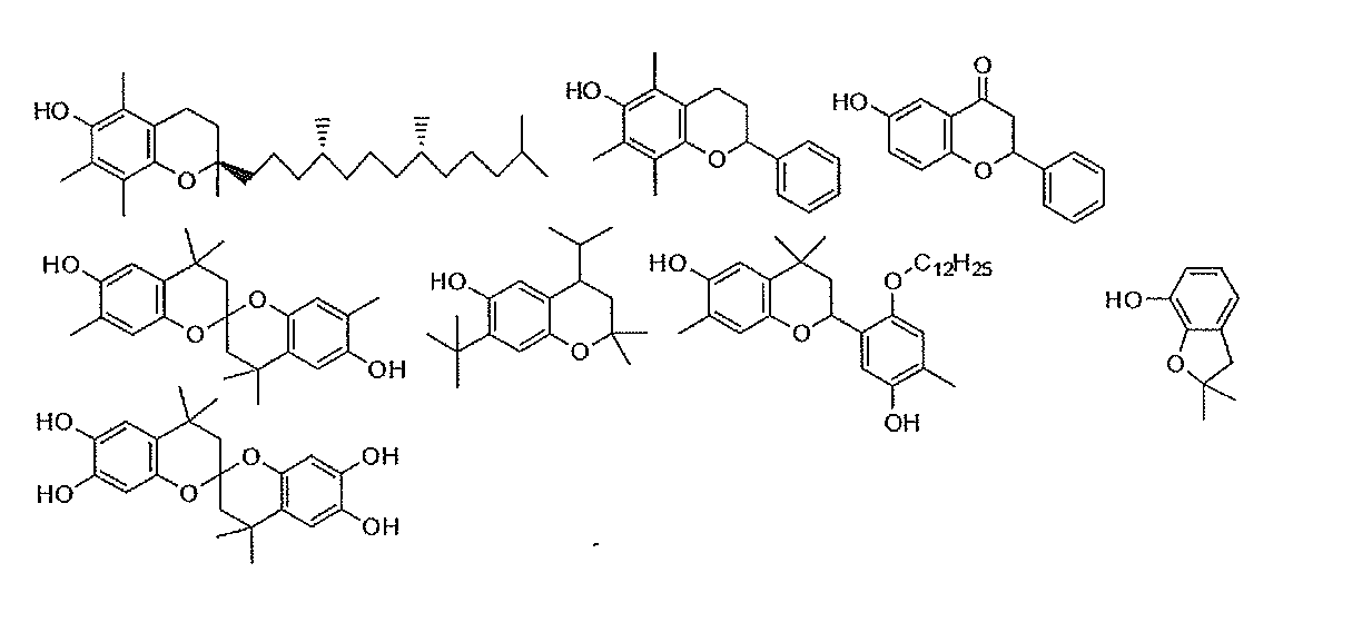
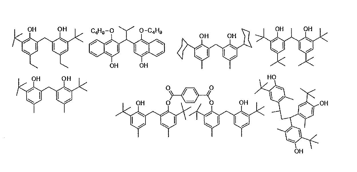
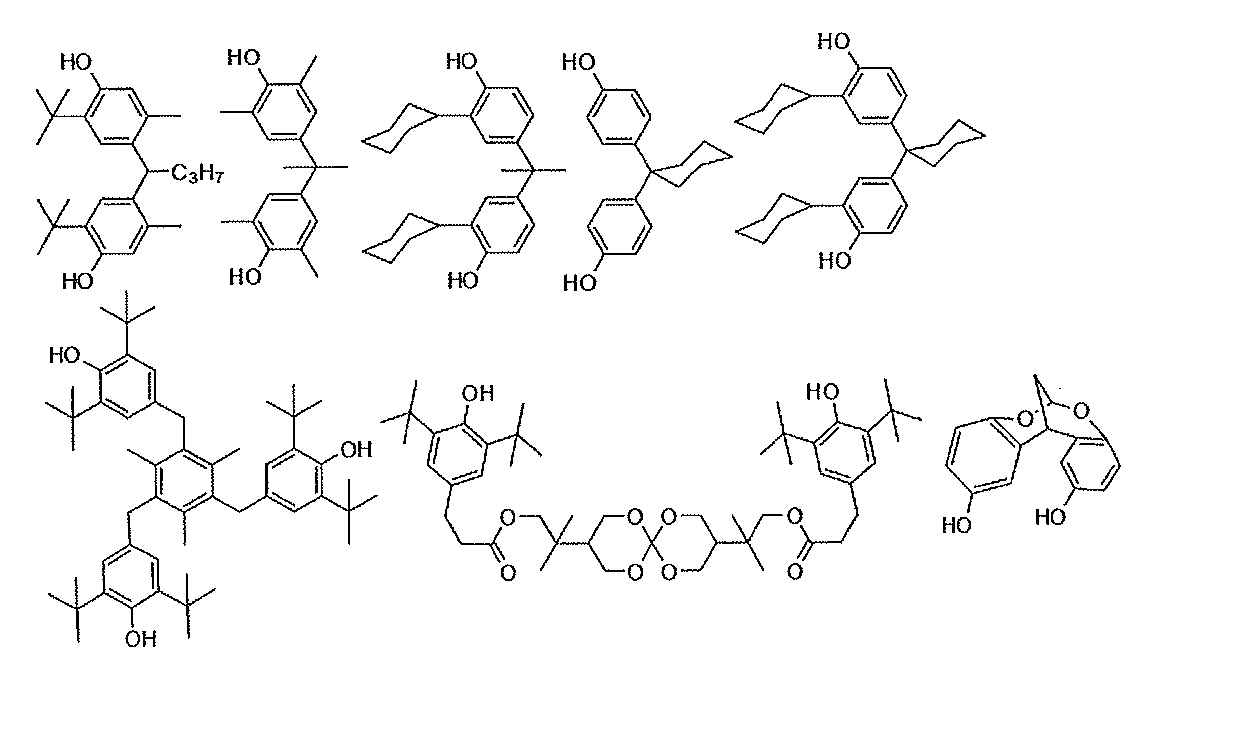
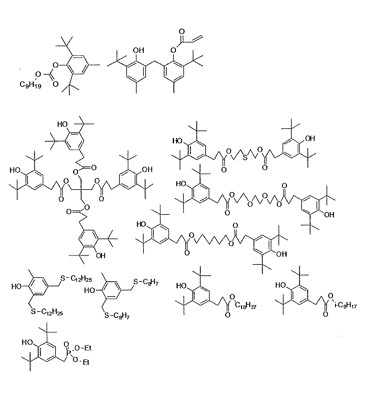
OCA30には、フェノール系化合物に加え、又はフェノール系化合物に代え、メルカプト基(-SH)基を有する複素環化合物(SH基含有複素環化合物)をマイグレーション防止剤として含めるようにしてもよい。該複素環化合物は、メルカプト基及び複素環部に含まれるヘテロ原子によって銀イオンを捕獲して、イオンマイグレーションを抑制する。
複素環化合物は、ヘテロ原子を少なくとも一つ持つ環状化合物である。ヘテロ原子とは、炭素原子及び水素原子以外の原子を意味する。ヘテロ原子は複素環の環系の構成部分を形成する原子のみを意味し、環系に対して外部に位置していたり、少なくとも一つの非共役単結合により環系から分離していたり、環系のさらなる置換基の一部分であるような原子は意味しない。ヘテロ原子の数の上限は特にないが、好ましくは10個以下であり、さらに好ましくは6個以下、特に好ましくは4個以下である。
これらの要件を満たす、いかなるSH基含有複素環化合物を用いてもよいが、ヘテロ原子として好ましくは、窒素原子、硫黄原子、酸素原子、セレン原子、テルル原子、リン原子、ケイ素原子又はホウ素原子であり、さらに好ましくは、窒素原子、硫黄原子又は酸素原子であり、特に好ましくは窒素原子又は硫黄原子である。
複素環の環員数は特に制限されないが、好ましくは4~10員環であり、より好ましくは5~9員環であり、さらに好ましくは5~6員環である。
複素環としては、芳香族及び非芳香族のいずれでもよいが、好ましくは芳香族複素環である。
複素環の構成は単環及び縮環のいずれでもよいが、好ましくは単環又は2個の芳香環からなる複素環である。
これらの複素環として具体的には、ピロール環、チオフェン環、フラン環、イミダゾール環、ピラゾール環、チアゾール環、イソチアゾール環、オキサゾール環、イソオキサゾール環、ピリジン環、ピラジン環、ピリミジン環、ピリダジン環、インドリジン環、トリアゾール環、オキサジアゾール環、チアジアゾール環、トリアザインデン環、テトラアザインデン環、ペンタアザインデン環、ヘキサアザインデン環、プリン環、テトラゾール環、ピラゾロトリアゾール環、ピロロトリアゾール環、及び、これらにベンゾ縮環したインドール環、ベンゾフラン環、ベンゾチオフェン環、イソベンゾフラン環、キノリジン環、キノリン環、フタラジン環、キノキサリン環、イソキノリン環、カルバゾール環、フェナントリジン環、フェナントロリン環、アクリジン環、ベンゾトリアゾール環、及び、これらが一部又は全部飽和したピロリジン環、ピロリン環、イミダゾリン環等が挙げられるが、これらに限定されるものではない。
SH基含有複素環化合物は、メルカプト基を有する。メルカプト基は銀と共有結合を生成する反応性に富む。このメルカプト基は、上記複素環部に結合する。
SH基含有複素環化合物中におけるメルカプト基の量は特に制限されないが、SH基含有複素環化合物の絶縁樹脂中での分散性がより良好である点より、化合物全分子量中に対してメルカプト基の原子量総量が占める割合が50%以下であることが好ましく、特に40%以下が好ましい。
なお、メルカプト基は、一つだけなく、複数含まれていてもよい。
SH基含有複素環化合物は、メルカプト基以外の置換基を有していてもよい。そのような置換基としては、例えば、ハロゲン原子、アルキル基、アルケニル基、アルキニル基、アリール基、シアノ基、ヒドロキシル基、ニトロ基、カルボキシル基、アルコキシ基、アリールオキシ基、シリルオキシ基、アシルオキシ基、カルバモイルオキシ基、アルコキシカルボニルオキシ基、アリールオキシカルボニルオキシ基、アミノ基、アンモニオ基、アシルアミノ基、アミノカルボニルアミノ基、アルコキシカルボニルアミノ基、アリールオキシカルボニルアミノ基、スルファモイルアミノ基、アルキル及びアリールスルホニルアミノ基、メルカプト基、アルキルチオ基、アリールチオ基、スルファモイル基、スルホ基、アルキル及びアリールスルフィニル基、アルキル及びアリールスルホニル基、アシル基、アリールオキシカルボニル基、アルコキシカルボニル基、カルバモイル基、イミド基、ホスフィノ基、ホスフィニル基、ホスフィニルオキシ基、ホスフィニルアミノ基、ホスホノ基、シリル基、ヒドラジノ基、ウレイド基、ボロン酸基(-B(OH)2)、ホスファト基(-OPO(OH) 2)、スルファト基(-OSO3H)等が挙げられる。
本発明は、上記した実施の形態に特に限定されるものではなく、本発明の主旨を逸脱しない範囲で種々の変更が可能である。
例えば、積層導電シート12は、図2及び図3に示すように、第1透明基体14Aの一主面に第1導電部16Aを形成し、第2透明基体14Bの一主面に第2導電部16Bを形成して積層するようにしたが、図5に示すように、第1透明基体14Aの一主面に第1導電部16Aを形成し、第1透明基体14Aの他主面に第2導電部16Bを形成するようにしてもよい。この場合、第2透明基体14Bが存在せず、第2導電部16B上に第1透明基体14Aが積層され、第1透明基体14A上に第1導電部16Aが積層された形態となる。
また、第1導電シート10Aと第2導電シート10Bとの間に他の層が存在してもよく、第1導電部16Aと第2導電部16Bとが絶縁を保たれた状態となるように絶縁層を介在させた態様の場合には、それらが対向して配置されてもよい。
さらに、セル22A、22Bは菱形形状に限定されるものではなく、平行四辺形であってもよい。勿論、この場合にも、セル22A、22Bには、銀細線20の交差角度が鈍角である対角と、鋭角である対角とが存在する。
以下、本発明につき実施例を挙げてさらに具体的に説明する。なお、以下の実施例に示される材料、使用量、割合、処理内容、処理手順等は、本発明の趣旨を逸脱しない限り適宜変更することができる。従って、本発明の範囲は以下に示す具体例により限定的に解釈されるべきものではない。
[OCA]
[OCA]
表1の記載に従い、各主成分、及び光重合開始剤として、イルガキュア651(チバ・ジャパン社製の2,2-ジメトキシ-2-フェニルアセトフェノンの商標。以下、「Irg651」と表記する)を0.04質量部秤量してガラス容器中でよく混合し、窒素ガスにて溶存酸素を置換した後、低圧水銀ランプで数分間紫外線を照射して部分的に重合させ、粘度1500cP程度の粘性液体を得た。得られた組成物に追加の重合開始剤(Irg651)0.15質量部を加え、十分に撹拌した。この混合物を真空脱泡した後、剥離処理をした50μm厚のポリエステルフイルム(剥離フイルム)の上に、乾燥後の膜厚が100μm厚となるように塗工し、重合を阻害する酸素を除去するためにさらに上記剥離フイルムを被せ、両面から低圧水銀ランプを約4分間照射し、透明粘着シートを得た。下記方法に従い、得られたシートのtanδ、貯蔵弾性率を測定した。測定結果を表1に示す。

[貯蔵弾性率及びtanδ(損失正接)(動的粘弾性特性)の測定方法]
(サンプルの作成)
上記方法で作製した透明粘着シートを積層した約3mm厚のシートを7.9mmφの抜き刃で打ち抜いて、円柱状のサンプルを得た。
(サンプルの作成)
上記方法で作製した透明粘着シートを積層した約3mm厚のシートを7.9mmφの抜き刃で打ち抜いて、円柱状のサンプルを得た。
(測定)
動的粘弾性特性は、Rheometric Scientific社製Advanced Rheometric Expansion System (ARES)を用いた。サンプル固定用治具は、7.9mmφのパラレルプレートを用い、上記の方法で作製したサンプルをプレートの間に配し、テンションを調整した。動的粘弾性特性の測定は空気中で行い、せん断モード、周波数1.0Hzにおいて、-50~200℃で昇温速度5℃/分で測定し、25℃における貯蔵弾性率G’(Pa)、及び140℃におけるtanδ(損失正接)を求めた。
動的粘弾性特性は、Rheometric Scientific社製Advanced Rheometric Expansion System (ARES)を用いた。サンプル固定用治具は、7.9mmφのパラレルプレートを用い、上記の方法で作製したサンプルをプレートの間に配し、テンションを調整した。動的粘弾性特性の測定は空気中で行い、せん断モード、周波数1.0Hzにおいて、-50~200℃で昇温速度5℃/分で測定し、25℃における貯蔵弾性率G’(Pa)、及び140℃におけるtanδ(損失正接)を求めた。
主成分、開始剤ないし架橋剤、マイグレーション防止剤の各具体的物質名とその配合割合、損失係数tanδ及び貯蔵弾性率を表1に纏めて示す。
また、2EHA、IOA、BA、ICA、IBXA、AA、DAAM、V♯190、HEA、HPAは、それぞれ、2-エチルヘキシルアクリレート、イソオクチルアクリレート、n-ブチルアクリレート、イソセチルアクリレート、イソボルニルアクリレート、アクリル酸、ダイアセトンアクリルアミド、エトキシエトキシエチルアクリレート、2-ヒドロキシエチルアクリレート、2-ヒドロキシプロピルアクリレートを表す。また、Irg651、V-65は、BASFジャパン社製、和光純薬社製の重合開始剤であり、HDDA(1,6-ヘキサンジオールアクリレート)、L-45(イソシアネート系)は架橋剤である。
さらに、化合物aはDL-α-トコフェロールであり、その還元電位は0.56Vである。また、化合物b、化合物cは、それぞれ、構造式が以下の式(6)、式(7)に示される物質であり、各々の還元電位は、1.09V、1.17Vである。

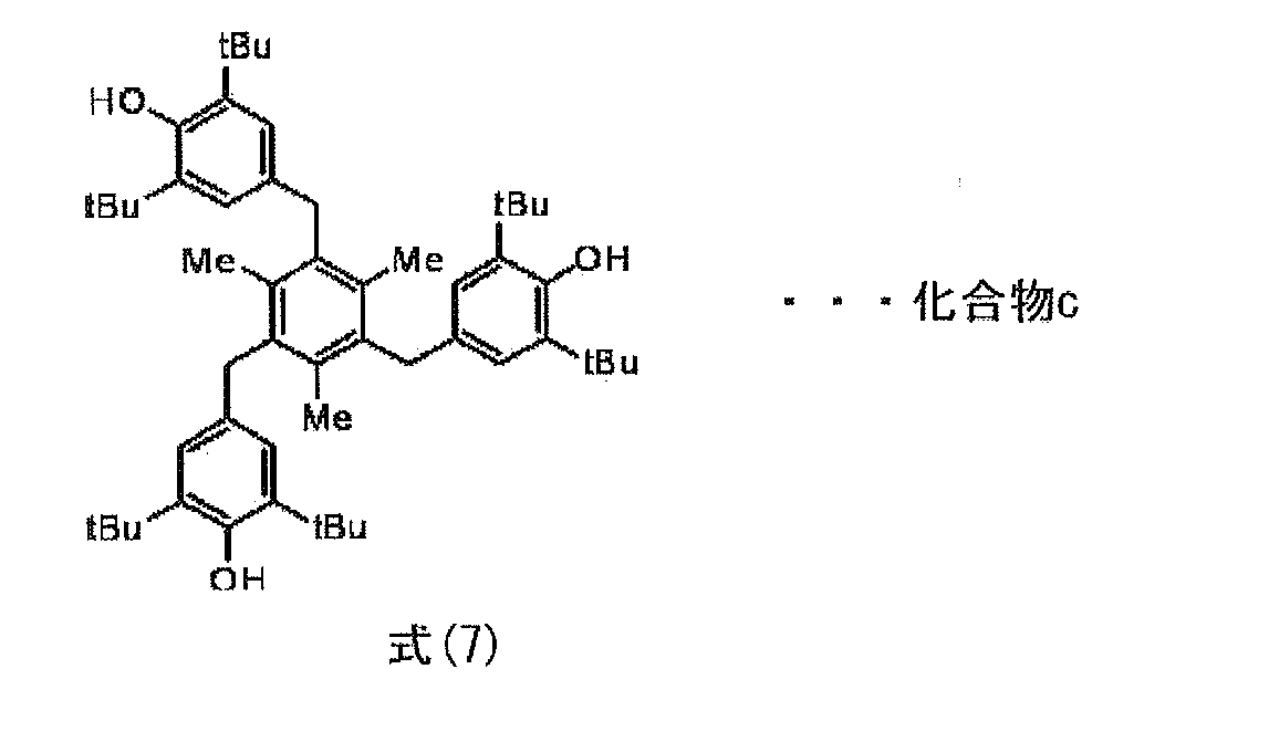
図6に示すPET基板50、52上のそれぞれに、特表2012-519329号公報の段落[0104]に記載された手順に従って、マイクロコンタクト印刷パターニング法によって銀細線をパターニングすることで長尺なメッシュ状の陽極54、陰極56を形成し、導電シート58、60を作製した。セルは菱形形状とした。
そして、導電シート58の一主面(陰極56が形成されている面)に対し、表1に示す合成例No.1~No.24のいずれかのOCA62を100μmで塗布した後、図7に示すように、陰極56と陽極54が互いに直交した状態で対向するようにして、OCA62上に導電シート60を載置した。これにより、Vモード評価用基材64を得た。なお、陰極56、陽極54には、それぞれ、直流電源66(電圧15V)の負極68、正極70を電気的に接続した。
陽極54と陰極56との交差箇所における重なり部分A(太線で囲繞した部分)の面積は、9mm2であった。
[評価用基材の作製2-Hモード]
[評価用基材の作製2-Hモード]
図8に示すPET基板72上に、特表2012-519329号公報の段落[0104]に記載された手順に従って、マイクロコンタクト印刷パターニング法によって銀細線をパターニングすることで、長尺で且つ互いに平行に並列配置されたメッシュ状の陽極54、ダミー電極74及び陰極56を形成し、導電シート76を作製した。セルは菱形形状とした。また、陽極54及び陰極56の幅方向寸法は3mm、ダミー電極74の幅方向寸法は2mm、陽極54とダミー電極74との間のクリアランス(スペース間隔)、及びダミー電極74と陰極56との間のクリアランス(スペース間隔)は50μmとした。
そして、該導電シート76の一主面(陽極54、ダミー電極74及び陰極56が形成されている面)に対し、図9に示すように、表1中の合成例No.1~No.24のいずれかの100μm厚のOCA62を貼り合わせた後、該OCA62上にPET基板78を載置した。これにより、Hモード評価用基材80を得た。Vモード評価用基材64と同様に、陰極56、陽極54には、それぞれ、直流電源66(電圧15V)の負極68、正極70を電気的に接続した。
なお、上記の例ではマイクロコンタクト印刷パターニング法で評価用基材を作製するようにしているが、銀塩法によって作製することも可能である。すなわち、後述する実施例36は、メッシュ電極を銀塩法によって作製したことを除いては実施例30と同様にして得られたものである。
[評価1-銀のマイグレーション]
Vモード評価用基材64については、陰極56と陽極54間の抵抗値の変化で銀のマイグレーションの度合いを評価した。具体的には、80℃、相対湿度85%、1気圧の環境下で該抵抗値が1×10⁵Ωに低下するまでの時間を測定し、40時間以上のものを良好(A)、30時間以上40時間未満のものを許容範囲(B)、30時間未満であったものを不足(C)と評価した。
Vモード評価用基材64については、陰極56と陽極54間の抵抗値の変化で銀のマイグレーションの度合いを評価した。具体的には、80℃、相対湿度85%、1気圧の環境下で該抵抗値が1×10⁵Ωに低下するまでの時間を測定し、40時間以上のものを良好(A)、30時間以上40時間未満のものを許容範囲(B)、30時間未満であったものを不足(C)と評価した。
一方、Hモード評価用基材80では、陽極54の抵抗変化率で銀のマイグレーションの度合いを評価した。すなわち、Hモード評価用基材80を80℃、相対湿度85%、1気圧の環境下で駆動して100時間経過した際の陽極54の抵抗変化率を測定し、初期からの抵抗変化率が5%未満であるものを良好(A)、5%以上10%未満であるものを許容範囲(B)、10%以上のものを不足(C)と評価した。
[評価2-視認性]
Hモード評価用基材80につき、上記に従って100時間駆動した後の電極の視認性に関する官能評価を行った。すなわち、線太り、交点太り、又はデンドライト発生に伴う電極形状の変化によって銀細線が見えるようになったものを不良(C)、銀細線がやや見えるようになったものを許容範囲(B)、銀細線が未だ見えないものを良好(A)と評価した。
Hモード評価用基材80につき、上記に従って100時間駆動した後の電極の視認性に関する官能評価を行った。すなわち、線太り、交点太り、又はデンドライト発生に伴う電極形状の変化によって銀細線が見えるようになったものを不良(C)、銀細線がやや見えるようになったものを許容範囲(B)、銀細線が未だ見えないものを良好(A)と評価した。
[評価3-白化]
図10に示すように、ガラス基板82の一主面上に、表1の合成例No.1~No.24のいずれかのOCA62を介して、厚み50μmのPET基板84を載置することで白化評価試験用基材86を得た。その後、65℃、相対湿度95%の環境下に72時間暴露し、さらに、23℃、相対湿度50%の環境下に暴露して、ヘイズが3%以下に達するまでの時間を測定した。この測定には、村上色彩技術研究所社製のHR-100を用いた。
図10に示すように、ガラス基板82の一主面上に、表1の合成例No.1~No.24のいずれかのOCA62を介して、厚み50μmのPET基板84を載置することで白化評価試験用基材86を得た。その後、65℃、相対湿度95%の環境下に72時間暴露し、さらに、23℃、相対湿度50%の環境下に暴露して、ヘイズが3%以下に達するまでの時間を測定した。この測定には、村上色彩技術研究所社製のHR-100を用いた。
なお、ヘイズ(%)は、上記のようにして得られた透明両面粘着シートの一方の片面上の剥離PETフイルムを剥がして、粘着性を示す一方の表面を光学PETフイルム(東レ製コスモシャイン)に張り合わせ、他方の剥離PETフイルムを剥がしてガラス(ダウコーニング製 EAGLE XG)に貼り合わせ、50℃、5気圧条件に30分曝した後、25℃、50%条件に24時間静置した後、東京電色社製ヘイズメーターMODEL TC-H3を用いて測定した。
そして、ヘイズが3%以下に達するまでの時間が6時間未満であるものを良好(A)、6~12時間の範囲内であるものを許容範囲(B)、12時間を超えるものを不良(C)と評価した。
[評価結果]
以上の評価結果を、菱形形状のセルの鋭角の角度、セルピッチ、線幅、用いたOCA62の合成例No.及び物性値とともに、実施例1~18及び比較例1~3として表2に一括して示す。この表2から、セルが菱形で線幅4μm以下のメッシュ電極と、損失係数(tanδ)が0.13以上であり、且つ貯蔵弾性率が8.9×10⁴Pa以下であるOCA62とを採用することにより、マイグレーションが起こることを防止することができるとともに、視認性に優れるタッチパネルが得られることが分かる。
以上の評価結果を、菱形形状のセルの鋭角の角度、セルピッチ、線幅、用いたOCA62の合成例No.及び物性値とともに、実施例1~18及び比較例1~3として表2に一括して示す。この表2から、セルが菱形で線幅4μm以下のメッシュ電極と、損失係数(tanδ)が0.13以上であり、且つ貯蔵弾性率が8.9×10⁴Pa以下であるOCA62とを採用することにより、マイグレーションが起こることを防止することができるとともに、視認性に優れるタッチパネルが得られることが分かる。
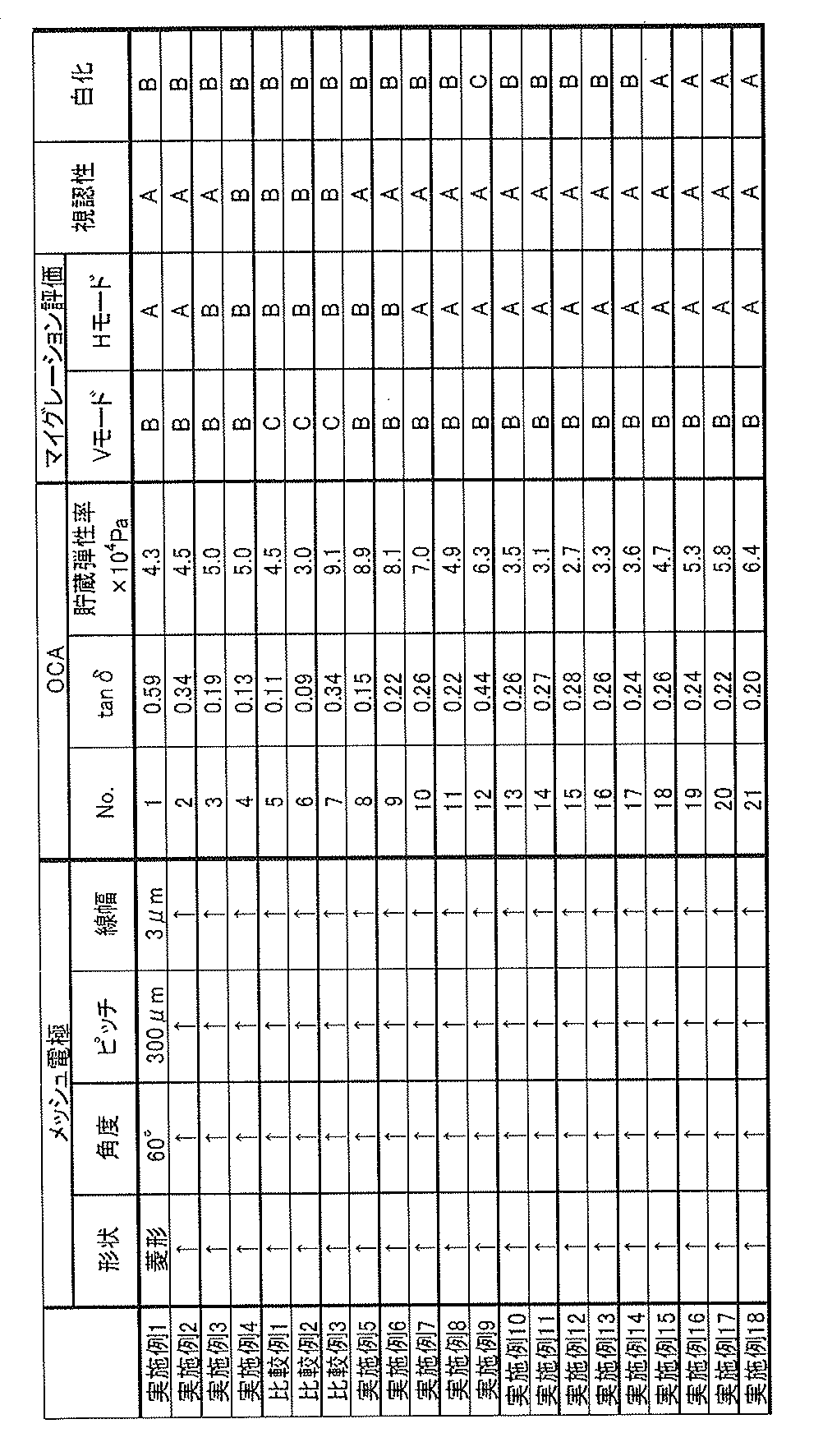
特に、OCA62が下記の(A)~(C)に示される成分を含むものである合成No.19、No.20、No.21である場合、白化特性も優れていることも分かる。
(A):ガラス転移点Tgが25℃以下であるアルキル(メタ)アクリレートモノマー(ただし、アルキル基は4~18個の炭素原子を有する)
(B):ガラス転移点Tgが25℃を超える(メタ)アクリレートモノマーのエステル
(C):ヒドロキシアルキル(メタ)アクリレート、非置換(メタ)アクリルアミド、N-アルキル置換(メタ)アクリルアミド、N,N-ジアルキル置換(メタ)アクリルアミド、尿素官能基を有するモノマー、ラクタム官能基、三級アミン、脂環式アミン、芳香族アミン、及びこれらの組み合わせを有するモノマーの群から選択されるモノマー
(A):ガラス転移点Tgが25℃以下であるアルキル(メタ)アクリレートモノマー(ただし、アルキル基は4~18個の炭素原子を有する)
(B):ガラス転移点Tgが25℃を超える(メタ)アクリレートモノマーのエステル
(C):ヒドロキシアルキル(メタ)アクリレート、非置換(メタ)アクリルアミド、N-アルキル置換(メタ)アクリルアミド、N,N-ジアルキル置換(メタ)アクリルアミド、尿素官能基を有するモノマー、ラクタム官能基、三級アミン、脂環式アミン、芳香族アミン、及びこれらの組み合わせを有するモノマーの群から選択されるモノマー
また、合成例No.20又はNo.8のOCA62を用いる一方で菱形形状のセルの鋭角の角度、セルピッチ、線幅等を種々変更し、上記の評価を行った。先ず、角度のみを変更した場合の評価結果を、実施例19~22として表3に示す。この表3から、セルの鋭角の角度が30°~70°の範囲内においても、マイグレーション、視認性及び白化の全てが良好又は許容範囲であるタッチパネルが得られることが分かる。

次に、表4はセルピッチのみを変更した場合(実施例23~26)の評価結果であり、表5は線幅のみを変更した場合(実施例27~29)の評価結果である。これら表4及び表5から、視認性に優れたセルピッチが300μm以下の範囲においても、また視認性に優れた線幅が2μm以下の範囲においてでも、マイグレーション、視認性及び白化が良好又は許容範囲であるタッチパネルが得られることが分かる。


表6に、OCA62にさらにフェノール系化合物からなるマイグレーション防止剤を含んだものを用いて、鋭角の角度、セルピッチ、線幅を種々変更した実施例30~36の評価結果を示す。この表6から、フェノール系化合物からなるマイグレーション防止剤を含んだOCA62を用いることにより、特にマイグレーション防止効果が高く、且つ視認性に優れるタッチパネルが得られることが明らかである。

最後に、実施例36より、メッシュ電極を銀塩法で形成した場合でも、マイクロコンタクト印刷パターニング法で形成したものと同様の効果が得られることが明らかである。
Claims (9)
- 絶縁層(14A)を介して対向する第1電極層(16A)と第2電極層(16B)を有するタッチパネル(100)において、
前記第1電極層(16A)では、第1の方向に沿って延在する第1電極(18A)が、前記第1の方向に対して直交する第2の方向に沿って複数個並列され、
前記第2電極層(16B)では、前記第2の方向に沿って延在する第2電極(18B)が、前記第1の方向に沿って複数個並列され、
前記第1電極(18A)又は前記第2電極(18B)の少なくともいずれか一方は、幅方向寸法が4μm以下である銀細線(20)から形成されたメッシュからなり、
前記メッシュは、前記銀細線(20)同士が交差することで形成されるセル(22A、22B)を複数個含み、
前記セル(22A、22B)の少なくとも1つは、前記銀細線(20)同士の交差によって形成される交差角度が鈍角である対角と、鋭角である対角とを有する平行四辺形形状をなし、
前記メッシュからなる前記第1電極(18A)又は前記第2電極(18B)の少なくともいずれか一方及び前記絶縁層(14A)に、140℃、1Hzでの損失係数tanδが0.13以上であり、且つ25℃、1Hzでの貯蔵弾性率が8.9×10⁴Pa以下である粘着剤(30)が配置されていることを特徴とするタッチパネル(100)。 - 請求項1記載のタッチパネル(100)において、平行四辺形形状をなす前記セル(22A、22B)での前記鋭角な対角では、前記銀細線(20)同士の交差角度が70°以下であることを特徴とするタッチパネル(100)。
- 請求項1記載のタッチパネル(100)において、平行四辺形形状をなす前記セル(22A、22B)が菱形形状であることを特徴とするタッチパネル(100)。
- 請求項1記載のタッチパネル(100)において、セルピッチが300μm以下であることを特徴とするタッチパネル(100)。
- 請求項1記載のタッチパネル(100)において、前記銀細線(20)の幅方向寸法が2μm以下であることを特徴とするタッチパネル(100)。
- 請求項1記載のタッチパネル(100)において、前記粘着剤(30)が下記の(A)~(C)に示される成分を含むものであることを特徴とするタッチパネル(100)。
(A):ガラス転移点Tgが25℃以下であるアルキル(メタ)アクリレートモノマー(ただし、アルキル基は4~18個の炭素原子を有する)
(B):ガラス転移点Tgが25℃を超える(メタ)アクリレートモノマーのエステル
(C):ヒドロキシアルキル(メタ)アクリレート、非置換(メタ)アクリルアミド、N-アルキル置換(メタ)アクリルアミド、N,N-ジアルキル置換(メタ)アクリルアミド、尿素官能基を有するモノマー、ラクタム官能基、三級アミン、脂環式アミン、芳香族アミン、及びこれらの組み合わせを有するモノマーの群から選択されるモノマー - 請求項1記載のタッチパネル(100)において、前記粘着剤(30)が、フェノール系化合物からなるマイグレーション防止剤をさらに含むことを特徴とするタッチパネル(100)。
- 請求項1記載のタッチパネル(100)において、前記メッシュからなる前記第1電極(18A)又は前記第2電極(18B)の少なくともいずれか一方が、マイクロコンタクト印刷パターニング法又は銀塩法によって形成されたものであることを特徴とするタッチパネル(100)。
- 請求項1に記載したタッチパネル(100)を含むことを特徴とする表示装置(108)。
Priority Applications (2)
| Application Number | Priority Date | Filing Date | Title |
|---|---|---|---|
| CN201480017837.5A CN105074636B (zh) | 2013-03-26 | 2014-02-17 | 触摸屏及显示装置 |
| US14/864,872 US9395863B2 (en) | 2013-03-26 | 2015-09-25 | Touch panel and display device |
Applications Claiming Priority (2)
| Application Number | Priority Date | Filing Date | Title |
|---|---|---|---|
| JP2013064316A JP5805127B2 (ja) | 2013-03-26 | 2013-03-26 | タッチパネル及び表示装置 |
| JP2013-064316 | 2013-03-26 |
Related Child Applications (1)
| Application Number | Title | Priority Date | Filing Date |
|---|---|---|---|
| US14/864,872 Continuation US9395863B2 (en) | 2013-03-26 | 2015-09-25 | Touch panel and display device |
Publications (1)
| Publication Number | Publication Date |
|---|---|
| WO2014156364A1 true WO2014156364A1 (ja) | 2014-10-02 |
Family
ID=51623365
Family Applications (1)
| Application Number | Title | Priority Date | Filing Date |
|---|---|---|---|
| PCT/JP2014/053585 Ceased WO2014156364A1 (ja) | 2013-03-26 | 2014-02-17 | タッチパネル及び表示装置 |
Country Status (5)
| Country | Link |
|---|---|
| US (1) | US9395863B2 (ja) |
| JP (1) | JP5805127B2 (ja) |
| CN (1) | CN105074636B (ja) |
| TW (1) | TWI601041B (ja) |
| WO (1) | WO2014156364A1 (ja) |
Cited By (3)
| Publication number | Priority date | Publication date | Assignee | Title |
|---|---|---|---|---|
| EP3026536A1 (en) * | 2014-11-25 | 2016-06-01 | LG Innotek Co., Ltd. | Touch window comprising mesh electrode |
| WO2016170943A1 (ja) * | 2015-04-21 | 2016-10-27 | 東レ株式会社 | 積層部材及びタッチパネル |
| WO2018029750A1 (ja) * | 2016-08-08 | 2018-02-15 | 東レ株式会社 | 積層部材及びタッチパネル |
Families Citing this family (14)
| Publication number | Priority date | Publication date | Assignee | Title |
|---|---|---|---|---|
| JP2016126480A (ja) * | 2014-12-26 | 2016-07-11 | 大日本印刷株式会社 | タッチパネルセンサ |
| CN104656987A (zh) * | 2015-01-21 | 2015-05-27 | 业成光电(深圳)有限公司 | 具有金属网格的透明导电结构 |
| WO2016136971A1 (ja) * | 2015-02-27 | 2016-09-01 | 株式会社フジクラ | タッチセンサ用配線体、タッチセンサ用配線基板及びタッチセンサ |
| CN107924247B (zh) * | 2015-10-07 | 2021-08-03 | 积水化学工业株式会社 | 触控面板用层间填充材料及触控面板层叠体 |
| KR20240125695A (ko) | 2015-10-07 | 2024-08-19 | 세키스이가가쿠 고교가부시키가이샤 | 터치 패널용 층간 충전 재료 및 터치 패널 적층체 |
| US20170269728A1 (en) * | 2016-03-15 | 2017-09-21 | Microsoft Technology Licensing, Llc | Rhombic mesh electrode matrix having periodic electrodes |
| WO2018047608A1 (ja) * | 2016-09-08 | 2018-03-15 | 富士フイルム株式会社 | 導電性フィルムの製造方法、導電性フィルム、タッチパネルセンサー、アンテナ、指紋認証部、および、タッチパネル |
| JP6888077B2 (ja) * | 2017-03-06 | 2021-06-16 | 富士フイルム株式会社 | 導電性部材およびタッチパネル |
| KR102419557B1 (ko) * | 2017-08-28 | 2022-07-08 | 엘지디스플레이 주식회사 | 터치 스크린 패널 및 이를 포함하는 표시 장치 |
| CN110751902B (zh) | 2018-07-24 | 2021-01-26 | 京东方科技集团股份有限公司 | 显示装置及其制备方法 |
| CN109375801B (zh) * | 2018-09-27 | 2021-06-22 | 广西中沛光电科技有限公司 | 一种触摸屏的贴合方法 |
| US11762517B2 (en) * | 2019-06-19 | 2023-09-19 | Nissha Co., Ltd. | Touch panel |
| US11603343B2 (en) | 2020-09-02 | 2023-03-14 | Ankh Life Sciences Limited | Inhibition of DYRK1A kinase |
| US11327619B2 (en) * | 2020-09-22 | 2022-05-10 | Elo Touch Solutions, Inc. | Touchscreen device with non-orthogonal electrodes |
Citations (1)
| Publication number | Priority date | Publication date | Assignee | Title |
|---|---|---|---|---|
| WO2013008827A1 (ja) * | 2011-07-11 | 2013-01-17 | 富士フイルム株式会社 | 導電性積層体、タッチパネル及び表示装置 |
Family Cites Families (11)
| Publication number | Priority date | Publication date | Assignee | Title |
|---|---|---|---|---|
| WO2009108758A2 (en) | 2008-02-28 | 2009-09-03 | 3M Innovative Properties Company | Touch screen sensor with low visibility conductors |
| TWI490303B (zh) * | 2008-12-01 | 2015-07-01 | Furukawa Electric Co Ltd | Wafer adhesive tape and wafer processing methods |
| US20100156811A1 (en) * | 2008-12-22 | 2010-06-24 | Ding Hua Long | New pattern design for a capacitive touch screen |
| JP2011074308A (ja) | 2009-10-01 | 2011-04-14 | Three M Innovative Properties Co | 透明粘着シート及びそれを含む画像表示装置 |
| JP5740124B2 (ja) * | 2010-09-29 | 2015-06-24 | リンテック株式会社 | 両面粘着テープ及びタッチパネル付き表示装置 |
| TWI567912B (zh) * | 2011-02-18 | 2017-01-21 | 富士軟片股份有限公司 | 導電片以及觸控面板 |
| WO2012141131A1 (ja) * | 2011-04-11 | 2012-10-18 | グンゼ株式会社 | タッチパネル装置 |
| JP5779535B2 (ja) * | 2012-03-30 | 2015-09-16 | 富士フイルム株式会社 | 導電性フイルム、それを備える表示装置及び導電性フイルムのパターンの決定方法 |
| US20140041999A1 (en) * | 2012-08-13 | 2014-02-13 | Samsung Electro-Mechanics Co., Ltd. | Touch panel |
| CN202854787U (zh) * | 2012-10-15 | 2013-04-03 | 深圳市帝晶光电股份有限公司 | 单面双层菱形结构电容式触摸屏 |
| JP2014191445A (ja) * | 2013-03-26 | 2014-10-06 | Fujifilm Corp | タッチパネル及び表示装置 |
-
2013
- 2013-03-26 JP JP2013064316A patent/JP5805127B2/ja active Active
-
2014
- 2014-02-17 WO PCT/JP2014/053585 patent/WO2014156364A1/ja not_active Ceased
- 2014-02-17 CN CN201480017837.5A patent/CN105074636B/zh active Active
- 2014-02-21 TW TW103105755A patent/TWI601041B/zh not_active IP Right Cessation
-
2015
- 2015-09-25 US US14/864,872 patent/US9395863B2/en active Active
Patent Citations (1)
| Publication number | Priority date | Publication date | Assignee | Title |
|---|---|---|---|---|
| WO2013008827A1 (ja) * | 2011-07-11 | 2013-01-17 | 富士フイルム株式会社 | 導電性積層体、タッチパネル及び表示装置 |
Cited By (8)
| Publication number | Priority date | Publication date | Assignee | Title |
|---|---|---|---|---|
| EP3026536A1 (en) * | 2014-11-25 | 2016-06-01 | LG Innotek Co., Ltd. | Touch window comprising mesh electrode |
| US9891769B2 (en) | 2014-11-25 | 2018-02-13 | Lg Innotek Co., Ltd. | Touch window |
| US10139980B2 (en) | 2014-11-25 | 2018-11-27 | Lg Innotek Co., Ltd. | Touch window |
| US10474305B2 (en) | 2014-11-25 | 2019-11-12 | Lg Innotek Co., Ltd. | Touch window |
| WO2016170943A1 (ja) * | 2015-04-21 | 2016-10-27 | 東レ株式会社 | 積層部材及びタッチパネル |
| JP6090537B1 (ja) * | 2015-04-21 | 2017-03-08 | 東レ株式会社 | 積層部材及びタッチパネル |
| US10275104B2 (en) | 2015-04-21 | 2019-04-30 | Toray Industries, Inc. | Laminate member and touch panel |
| WO2018029750A1 (ja) * | 2016-08-08 | 2018-02-15 | 東レ株式会社 | 積層部材及びタッチパネル |
Also Published As
| Publication number | Publication date |
|---|---|
| JP5805127B2 (ja) | 2015-11-04 |
| US9395863B2 (en) | 2016-07-19 |
| JP2014191441A (ja) | 2014-10-06 |
| TW201443737A (zh) | 2014-11-16 |
| CN105074636B (zh) | 2016-11-09 |
| US20160018932A1 (en) | 2016-01-21 |
| CN105074636A (zh) | 2015-11-18 |
| TWI601041B (zh) | 2017-10-01 |
Similar Documents
| Publication | Publication Date | Title |
|---|---|---|
| JP5805127B2 (ja) | タッチパネル及び表示装置 | |
| CN105122189B (zh) | 触摸屏及显示装置 | |
| US10464290B2 (en) | Pressure-sensitive adhesive sheet for touch panel, laminate for touch panel, and capacitance-type touch panel | |
| KR102528043B1 (ko) | 코팅층이 형성된 편광 필름, 점착제층이 형성된 편광 필름, 및 화상 표시 장치 | |
| CN102510888B (zh) | 双面粘合片、带剥离片的双面粘合片、其制造方法以及透明层叠体 | |
| JP5540847B2 (ja) | アクリル系粘着剤組成物および粘着フィルム | |
| CN104046309A (zh) | 粘合剂、粘合剂层、粘合片以及触控面板 | |
| CN109415612B (zh) | 粘附膜、包括其的光学构件和包括其的光学显示装置 | |
| CN103619977A (zh) | 粘合剂组合物、粘合剂层以及粘合片 | |
| CN102884147A (zh) | 光学薄膜用粘合剂层、粘合型光学薄膜及图像显示装置 | |
| JP6511659B2 (ja) | 光学フィルム用粘着剤層、及び光学フィルム用粘着フィルム | |
| CN108495903A (zh) | 用于制造无色且抗老化的基于聚丙烯酸酯的压敏胶粘剂配混物的方法 | |
| TWI636713B (zh) | 配線基板 | |
| CN103038305B (zh) | 结晶性金属氧化物导电膜用粘合剂以及使用该粘合剂的结晶性金属氧化物导电膜用粘合片 | |
| KR20160104613A (ko) | 광학용 점착제, 광학용 점착 테이프 및 적층체 | |
| CN103703089B (zh) | 用于电子纸显示装置的介电结合膜 | |
| JP2019038947A (ja) | 粘着剤組成物、粘着シートおよび積層体 | |
| JP6424180B2 (ja) | タッチパネル及び表示装置 | |
| CN103455191A (zh) | 复合式胶片结构及具有复合式胶片结构的触控面板 | |
| TWM434990U (en) | Composite plastic film structure and touch panel comprising such structure | |
| TW202338043A (zh) | 雙面黏著片、積層體及積層體的製造方法 | |
| JP2017200974A (ja) | 粘着シート及び積層体 |
Legal Events
| Date | Code | Title | Description |
|---|---|---|---|
| WWE | Wipo information: entry into national phase |
Ref document number: 201480017837.5 Country of ref document: CN |
|
| 121 | Ep: the epo has been informed by wipo that ep was designated in this application |
Ref document number: 14773091 Country of ref document: EP Kind code of ref document: A1 |
|
| NENP | Non-entry into the national phase |
Ref country code: DE |
|
| 122 | Ep: pct application non-entry in european phase |
Ref document number: 14773091 Country of ref document: EP Kind code of ref document: A1 |