WO2014155565A1 - 縦型半導体装置 - Google Patents
縦型半導体装置 Download PDFInfo
- Publication number
- WO2014155565A1 WO2014155565A1 PCT/JP2013/059023 JP2013059023W WO2014155565A1 WO 2014155565 A1 WO2014155565 A1 WO 2014155565A1 JP 2013059023 W JP2013059023 W JP 2013059023W WO 2014155565 A1 WO2014155565 A1 WO 2014155565A1
- Authority
- WO
- WIPO (PCT)
- Prior art keywords
- region
- impurity concentration
- semiconductor substrate
- channel stop
- electrode
- Prior art date
- Legal status (The legal status is an assumption and is not a legal conclusion. Google has not performed a legal analysis and makes no representation as to the accuracy of the status listed.)
- Ceased
Links
Images



Classifications
-
- H—ELECTRICITY
- H10—SEMICONDUCTOR DEVICES; ELECTRIC SOLID-STATE DEVICES NOT OTHERWISE PROVIDED FOR
- H10D—INORGANIC ELECTRIC SEMICONDUCTOR DEVICES
- H10D12/00—Bipolar devices controlled by the field effect, e.g. insulated-gate bipolar transistors [IGBT]
- H10D12/411—Insulated-gate bipolar transistors [IGBT]
- H10D12/441—Vertical IGBTs
-
- H—ELECTRICITY
- H10—SEMICONDUCTOR DEVICES; ELECTRIC SOLID-STATE DEVICES NOT OTHERWISE PROVIDED FOR
- H10D—INORGANIC ELECTRIC SEMICONDUCTOR DEVICES
- H10D30/00—Field-effect transistors [FET]
- H10D30/60—Insulated-gate field-effect transistors [IGFET]
-
- H—ELECTRICITY
- H10—SEMICONDUCTOR DEVICES; ELECTRIC SOLID-STATE DEVICES NOT OTHERWISE PROVIDED FOR
- H10D—INORGANIC ELECTRIC SEMICONDUCTOR DEVICES
- H10D30/00—Field-effect transistors [FET]
- H10D30/60—Insulated-gate field-effect transistors [IGFET]
- H10D30/63—Vertical IGFETs
-
- H—ELECTRICITY
- H10—SEMICONDUCTOR DEVICES; ELECTRIC SOLID-STATE DEVICES NOT OTHERWISE PROVIDED FOR
- H10D—INORGANIC ELECTRIC SEMICONDUCTOR DEVICES
- H10D30/00—Field-effect transistors [FET]
- H10D30/60—Insulated-gate field-effect transistors [IGFET]
- H10D30/64—Double-diffused metal-oxide semiconductor [DMOS] FETs
- H10D30/66—Vertical DMOS [VDMOS] FETs
- H10D30/665—Vertical DMOS [VDMOS] FETs having edge termination structures
-
- H—ELECTRICITY
- H10—SEMICONDUCTOR DEVICES; ELECTRIC SOLID-STATE DEVICES NOT OTHERWISE PROVIDED FOR
- H10D—INORGANIC ELECTRIC SEMICONDUCTOR DEVICES
- H10D62/00—Semiconductor bodies, or regions thereof, of devices having potential barriers
- H10D62/10—Shapes, relative sizes or dispositions of the regions of the semiconductor bodies; Shapes of the semiconductor bodies
- H10D62/102—Constructional design considerations for preventing surface leakage or controlling electric field concentration
- H10D62/103—Constructional design considerations for preventing surface leakage or controlling electric field concentration for increasing or controlling the breakdown voltage of reverse-biased devices
- H10D62/105—Constructional design considerations for preventing surface leakage or controlling electric field concentration for increasing or controlling the breakdown voltage of reverse-biased devices by having particular doping profiles, shapes or arrangements of PN junctions; by having supplementary regions, e.g. junction termination extension [JTE]
-
- H—ELECTRICITY
- H10—SEMICONDUCTOR DEVICES; ELECTRIC SOLID-STATE DEVICES NOT OTHERWISE PROVIDED FOR
- H10D—INORGANIC ELECTRIC SEMICONDUCTOR DEVICES
- H10D62/00—Semiconductor bodies, or regions thereof, of devices having potential barriers
- H10D62/10—Shapes, relative sizes or dispositions of the regions of the semiconductor bodies; Shapes of the semiconductor bodies
- H10D62/102—Constructional design considerations for preventing surface leakage or controlling electric field concentration
- H10D62/103—Constructional design considerations for preventing surface leakage or controlling electric field concentration for increasing or controlling the breakdown voltage of reverse-biased devices
- H10D62/105—Constructional design considerations for preventing surface leakage or controlling electric field concentration for increasing or controlling the breakdown voltage of reverse-biased devices by having particular doping profiles, shapes or arrangements of PN junctions; by having supplementary regions, e.g. junction termination extension [JTE]
- H10D62/106—Constructional design considerations for preventing surface leakage or controlling electric field concentration for increasing or controlling the breakdown voltage of reverse-biased devices by having particular doping profiles, shapes or arrangements of PN junctions; by having supplementary regions, e.g. junction termination extension [JTE] having supplementary regions doped oppositely to or in rectifying contact with regions of the semiconductor bodies, e.g. guard rings with PN or Schottky junctions
-
- H—ELECTRICITY
- H10—SEMICONDUCTOR DEVICES; ELECTRIC SOLID-STATE DEVICES NOT OTHERWISE PROVIDED FOR
- H10D—INORGANIC ELECTRIC SEMICONDUCTOR DEVICES
- H10D62/00—Semiconductor bodies, or regions thereof, of devices having potential barriers
- H10D62/10—Shapes, relative sizes or dispositions of the regions of the semiconductor bodies; Shapes of the semiconductor bodies
- H10D62/102—Constructional design considerations for preventing surface leakage or controlling electric field concentration
- H10D62/103—Constructional design considerations for preventing surface leakage or controlling electric field concentration for increasing or controlling the breakdown voltage of reverse-biased devices
- H10D62/105—Constructional design considerations for preventing surface leakage or controlling electric field concentration for increasing or controlling the breakdown voltage of reverse-biased devices by having particular doping profiles, shapes or arrangements of PN junctions; by having supplementary regions, e.g. junction termination extension [JTE]
- H10D62/109—Reduced surface field [RESURF] PN junction structures
-
- H—ELECTRICITY
- H10—SEMICONDUCTOR DEVICES; ELECTRIC SOLID-STATE DEVICES NOT OTHERWISE PROVIDED FOR
- H10D—INORGANIC ELECTRIC SEMICONDUCTOR DEVICES
- H10D62/00—Semiconductor bodies, or regions thereof, of devices having potential barriers
- H10D62/10—Shapes, relative sizes or dispositions of the regions of the semiconductor bodies; Shapes of the semiconductor bodies
- H10D62/102—Constructional design considerations for preventing surface leakage or controlling electric field concentration
- H10D62/112—Constructional design considerations for preventing surface leakage or controlling electric field concentration for preventing surface leakage due to surface inversion layers, e.g. by using channel stoppers
-
- H—ELECTRICITY
- H10—SEMICONDUCTOR DEVICES; ELECTRIC SOLID-STATE DEVICES NOT OTHERWISE PROVIDED FOR
- H10D—INORGANIC ELECTRIC SEMICONDUCTOR DEVICES
- H10D62/00—Semiconductor bodies, or regions thereof, of devices having potential barriers
- H10D62/60—Impurity distributions or concentrations
-
- H—ELECTRICITY
- H10—SEMICONDUCTOR DEVICES; ELECTRIC SOLID-STATE DEVICES NOT OTHERWISE PROVIDED FOR
- H10D—INORGANIC ELECTRIC SEMICONDUCTOR DEVICES
- H10D64/00—Electrodes of devices having potential barriers
- H10D64/111—Field plates
-
- H—ELECTRICITY
- H10—SEMICONDUCTOR DEVICES; ELECTRIC SOLID-STATE DEVICES NOT OTHERWISE PROVIDED FOR
- H10D—INORGANIC ELECTRIC SEMICONDUCTOR DEVICES
- H10D62/00—Semiconductor bodies, or regions thereof, of devices having potential barriers
- H10D62/10—Shapes, relative sizes or dispositions of the regions of the semiconductor bodies; Shapes of the semiconductor bodies
- H10D62/102—Constructional design considerations for preventing surface leakage or controlling electric field concentration
- H10D62/103—Constructional design considerations for preventing surface leakage or controlling electric field concentration for increasing or controlling the breakdown voltage of reverse-biased devices
- H10D62/105—Constructional design considerations for preventing surface leakage or controlling electric field concentration for increasing or controlling the breakdown voltage of reverse-biased devices by having particular doping profiles, shapes or arrangements of PN junctions; by having supplementary regions, e.g. junction termination extension [JTE]
- H10D62/106—Constructional design considerations for preventing surface leakage or controlling electric field concentration for increasing or controlling the breakdown voltage of reverse-biased devices by having particular doping profiles, shapes or arrangements of PN junctions; by having supplementary regions, e.g. junction termination extension [JTE] having supplementary regions doped oppositely to or in rectifying contact with regions of the semiconductor bodies, e.g. guard rings with PN or Schottky junctions
- H10D62/107—Buried supplementary regions, e.g. buried guard rings
-
- H—ELECTRICITY
- H10—SEMICONDUCTOR DEVICES; ELECTRIC SOLID-STATE DEVICES NOT OTHERWISE PROVIDED FOR
- H10D—INORGANIC ELECTRIC SEMICONDUCTOR DEVICES
- H10D8/00—Diodes
Definitions
- the resistance between the front surface electrode formed on the surface of the semiconductor substrate and the back surface electrode formed on the back surface changes, and the current flows between the front surface electrode and the back surface electrode.
- a vertical semiconductor device that can be switched between non-off states.
- Patent Document 1 discloses the above vertical semiconductor device.
- the vertical semiconductor device disclosed in Patent Document 1 includes a gate electrode, and is switched between an on state and an off state by a voltage applied to the gate electrode. In the case of a diode, it is turned on when a forward voltage is applied and turned off when a reverse voltage is applied. In the vertical semiconductor device used for power control, the voltage difference applied between the front electrode and the back electrode is large. When the semiconductor device is off, the front electrode and the back electrode are turned off against the large voltage difference. It is necessary to keep (insulate).
- the semiconductor device is formed on a semiconductor substrate having a finite size, and when the voltage difference applied between the front electrode and the back electrode becomes large, the front electrode and the back electrode are interposed through the peripheral region of the semiconductor substrate. A phenomenon occurs in which current flows between them. Therefore, a semiconductor structure that actively switches on / off using a gate electrode or a semiconductor structure that performs rectifying operation using a PN junction or the like is arranged in the center of a semiconductor substrate, and a region that goes around the semiconductor (that is, a semiconductor) A technique in which a pressure-resistant structure is arranged in a region extending along the periphery of the substrate is widespread.
- the breakdown voltage structure here refers to a structure that suppresses current from flowing between the front electrode and the back electrode even when a large voltage difference is applied between the front electrode and the back electrode while the semiconductor device is in the off state. It is.
- the peripheral breakdown voltage structure of Patent Document 1 includes a guard ring that makes a round around the outer periphery of the central region 28 of the semiconductor substrate 12 and a channel stop region that makes a round around the outer circumference of the guard ring.
- a five-fold guard ring 14 is used (in FIG. 7, two outer guard rings 14d and 14e out of the five guard rings 14 are shown), and the impurity concentrations are different.
- a channel stop region 10 is formed by the regions 10g and 10h.
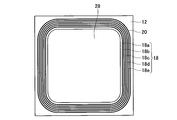
- Field electrodes 18 a to 18 e are disposed along the guard rings 14 a to 14 e, and a stopper electrode 20 is disposed along the channel stop region 10.
- FIG. 6 five-fold field electrodes 18a to 18e and a single stopper electrode 20 are shown.
- an IGBT is formed in the central region 28.
- reference numeral 2 is a back surface electrode (collector electrode) formed on the back surface of the semiconductor substrate 12
- reference number 4 is a p-type collector region
- reference number 8 is an n-type drift region.
- an n-type emitter region (not shown), a p-type body region that separates the n-type emitter region and the n-type drift region 8, and a gate insulating film interposed between the p-type body region.
- a surface electrode (emitter electrode) formed on the surface of the semiconductor substrate 12 and conducting to the emitter region.
- Reference numeral 16 is an insulating film which insulates the gate electrode and the emitter electrode, insulates the emitter electrode and the field electrode 18a, insulates between adjacent field electrodes, and insulates the field electrode 18e and the stopper electrode 20 from each other. is doing.
- the depletion layer spreads toward the outer peripheral side surface 12a of the semiconductor substrate 12 while the IGBT is off.
- the withstand voltage increases.
- the depletion layer reaches the outer peripheral side surface 12 a of the semiconductor substrate 12, the withstand voltage decreases.
- the n-type channel stop region 10 and the stopper electrode 20 prevent the depletion layer from reaching the outer peripheral side surface 12 a of the semiconductor substrate 12.
- the depletion layer is expanded toward the outer peripheral side surface 12a of the semiconductor substrate 12 by the p-type guard rings 14a to 14e and the field electrodes 18a to 18e, and the depletion is performed by the n-type channel stop region 10 and the stopper electrode 20.
- the layer is prevented from reaching the outer peripheral side surface 12 a of the semiconductor substrate 12.
- the technique of Patent Document 1 does not disclose the purpose of forming the channel stop region 10 by two regions 10g and 10h having different impurity concentrations, the impurity concentration is high in a local range in the region 10g having a low impurity concentration.
- Region 10h is formed. That is, not only the high impurity concentration region 10h is included in the low impurity concentration region 10g when the semiconductor substrate is viewed in plan, but also when the semiconductor substrate is viewed in cross section, the high impurity concentration region 10h is the low impurity concentration region 10g. Contained within. That is, the high impurity concentration region 10 h remains in a shallower range than the low impurity concentration region 10 g, and the high impurity concentration region 10 h does not contact the drift region 8.
- the depletion layer expanded toward the outer peripheral side surface 12a of the semiconductor substrate 12 by the guard rings 14a to 14e and the field electrodes 18a to 18e can be prevented from reaching the outer peripheral side surface 12a of the semiconductor substrate 12.
- the technique of Patent Document 1 there remains a problem that the interval between equipotential lines becomes narrow in the vicinity of the channel stop region 10 and the electric field strength increases.
- a problem remains that the interval between equipotential lines in the range 30 adjacent to the corner portion (corner portion when viewed in cross section) of the channel stop region 10 is narrowed, and the electric field strength is increased.
- a peripheral breakdown voltage structure is formed in the peripheral region of the semiconductor substrate.
- the peripheral breakdown voltage structure includes a channel stop region formed in a range facing the outer peripheral side surface of the semiconductor substrate and the surface continuing to the outer peripheral side surface. Inside the channel stop region, a structure such as a guard ring or a RESURF structure is formed that widens the depletion layer toward the outer peripheral side surface of the semiconductor substrate.
- the channel stop region satisfies the following relationship.
- a channel stop region is formed by a plurality of regions having different impurity concentrations, (2) The closer to the outer peripheral side of the semiconductor substrate, the higher the impurity concentration, (3) The depth of the high impurity concentration region is equal to or greater than the depth of the low impurity concentration region.
- “above” means that the depth of the high impurity concentration region is equal to the depth of the low impurity concentration region or deeper than the depth of the low impurity concentration region. That is, it means that the high impurity concentration region is not shallower than the low impurity concentration region. Since the impurity concentration is higher as the outer peripheral side of the semiconductor substrate is closer, the depth of the channel stop region near the outer peripheral side of the semiconductor substrate is more than the depth of the channel stop region far from the outer peripheral side of the semiconductor substrate Good.
- a channel stop region is formed by a plurality of regions having different impurity concentrations, (2) The closer to the outer peripheral side of the semiconductor substrate, the higher the impurity concentration, (3) If the high impurity concentration region is not shallower than the low impurity concentration region, the electric field strength in the range adjacent to the corner portion (corner portion when viewed in cross section) of the channel stop region is reduced, and the withstand voltage capability Can be improved.
- a channel stop region is formed by a plurality of regions having different impurity concentrations, (2) The relationship that the impurity concentration increases as it approaches the outer peripheral side surface of the semiconductor substrate is satisfied. However, the high impurity concentration region is formed shallower than the low impurity concentration region, and does not satisfy the relationship (3). (1) Even if the requirements of (2) are provided, if the relationship of (3) is lacking, the electric field strength of the drift layer in the range adjacent to the corner portion of the channel stop region (corner portion when viewed in cross section) is As a result, the pressure capacity cannot be improved.
- FIG. 2 is a diagram showing equipotential lines generated in the semiconductor substrate of FIG. 1.
- region The figure which looked at the peripheral part of the semiconductor substrate of 2nd Example in cross section.
- FIG. The figure which looked at the peripheral part of the semiconductor substrate of patent document 1 in cross section.
- FIG. 1 The figure which contrasts the phenomenon which arises in the peripheral part of the semiconductor substrate of 1st Example, and the peripheral part of the semiconductor substrate of patent document 1.
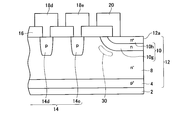
- FIG. 1 is a cross-sectional view of the periphery of the semiconductor substrate 12 of the first embodiment, showing the outer peripheral side surface 12a side of the outermost guard ring 14e.
- Multiple guard rings 14a to 14d are formed inside the outermost guard ring 14e, and a semiconductor structure that operates as an IGBT is formed inside thereof. These points are the same as those of the prior art, and redundant description is omitted.
- the IGBT described in Patent Document 1 uses a gate electrode extending along the surface of the semiconductor substrate, but may be an IGBT using a trench gate electrode.
- reference numeral 12 denotes a semiconductor substrate, and a back electrode (collector electrode) 2 is formed on the back surface of the semiconductor substrate 12.
- Reference number 4 is a p-type collector region
- reference number 6 is an n-type buffer region
- reference number 8 is an n-type drift region. Compared to the impurity concentration of the buffer region 6, the impurity concentration of the drift region 8 is low.
- the drift region 8 is composed of the semiconductor substrate 12 that remains without being processed, and may be called a bulk region.
- an n-type emitter region not shown, a p-type body region that separates the n-type emitter region and the n-type drift region 8, and a gate insulating film interposed in the body region And a surface electrode (emitter electrode) formed on the surface of the semiconductor substrate 12 and conducting to the emitter region.
- Reference numeral 16 is an insulating film, which insulates the gate electrode and the emitter electrode.
- Reference numeral 14e is the outermost guard ring, and reference numeral 18e is the outermost field electrode. The guard ring 14e and the field electrode 18e are electrically connected through an opening 16e formed in the insulating film 16.
- Guard rings 14a-14e are formed of p-type regions.
- Reference numeral 10 denotes a channel stop region, which is formed in a range facing the outer peripheral side surface 12a of the semiconductor substrate 12 and the surface 12b of the semiconductor substrate 12 following the outer peripheral side surface 12a.
- the channel stop region 10 is (1) It is formed of a plurality of n-type regions 10a, 10b, 10c, and 10d having different impurity concentrations, (2) The impurity concentration is higher as the outer peripheral side surface 12a of the semiconductor substrate 12 is approached. That is, the impurity concentration of the region 10a ⁇ the impurity concentration of the region 10b ⁇ the impurity concentration of the region 10c ⁇ the impurity concentration of the region 10d.
- the impurity concentration is higher than the impurity concentration in the drift region 8. That is, the impurity concentration of drift region 8 ⁇ the impurity concentration of region 10a.
- the region 10d is included in the region 10c
- the region 10c is included in the region 10b
- the region 10b is included in the region 10b
- the region 10b is included in the region 10b
- the region 10b is included in the region 10b
- the regions 10 b, 10 c, and 10 d do not contact the drift region 8, and only the region 10 a contacts the drift region 8.
- each of the regions 10a, 10b, 10c, and 10d is in contact with the drift region 8. become.
- the positions where the equipotential lines are concentrated and the electric field strength is likely to increase are dispersed at four locations indicated by reference numeral 30 in FIG. 1, and the electric field strength at each location is lowered.
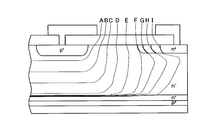
- FIG. 2 shows the distribution of equipotential lines A, B,... In a state where no on-voltage is applied to the gate electrode, the front electrode is grounded, and a positive voltage is applied to the back electrode.
- the equipotential lines are not dense even at the position indicated by the location 30 in FIG. 1, and the electric field strength at the location 30 is kept low.
- FIG. 3 shows the distribution of equipotential lines generated when the channel stop region 10p is formed in one region having the same concentration.
- the equipotential lines G1, H1, and I1 passing through the channel stop region 10p are densely arranged, and a high electric field strength is generated in the drift region 8 located around the channel stop region 10p.
- FIG. 2 and FIG. 3 are compared, when the channel stop region satisfies the relationships (1), (2), and (3), the maximum value of the electric field strength generated in the drift region 8 can be suppressed low. It is difficult to generate a phenomenon in which the electric field strength becomes too high and the insulation is broken.
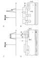
- FIG. 8 shows a comparison between phenomena occurring in the semiconductor device of the embodiment and a conventional semiconductor device.
- (2) of FIG. 8 shows a cross section of the semiconductor device of the embodiment shown in FIG. 1, and the electric field intensity distribution along the line (1)-(1) is a graph of (1) of FIG. (4) of FIG. 8 shows a cross section of the conventional semiconductor device shown in FIG. 7, and the electric field intensity distribution along the line (3)-(3) is a graph of (3) of FIG.
- (1) and (3) are compared, when the impurity concentration of the channel stop region 10 changes on the surface in contact with the drift region 8 as shown in (2), the position facing the portion where the concentration changes.
- the position where the impurity concentration changes from the drift region 8 having a low impurity concentration to the channel stop region 10a having a higher impurity concentration, and the region 10a having the lowest impurity concentration in the channel stop region 10 has a concentration lower than that.
- the position that changes from the area 10b to the area 10c that has a higher density, and the position that changes from the area 10c to the area 10d that has a higher density It is possible to prevent the phenomenon that the electric field concentration is dispersed and the electric field strength becomes too high and the insulation is broken.
- the area (value obtained by integrating the electric field strength along the distance) in the graph of (1) increases, and a high dielectric strength can be obtained.
- the impurity concentration of the channel stop region 10 on the surface in contact with the drift region 8 is uniform (the high impurity concentration region 10h is included in the low impurity concentration region 10g).
- the phenomenon of dispersing the electric field concentration can be obtained only around the position where the drift region 8 having a low impurity concentration changes to the channel stop region 10g having a higher impurity concentration than the drift region 8 having a low impurity concentration. It tends to occur when the insulation becomes too high.
- the electric field strength also decreases in the vicinity of the position where the region 10g having a low impurity concentration changes to the region 10h having a higher concentration than that, but since the change point of the impurity concentration does not face the drift region 8, the electric field concentration is dispersed. The effect is low, and the phenomenon that the maximum value of the electric field strength becomes too high cannot be suppressed. Moreover, the area in the graph of (3) is smaller than that of (1) and the dielectric strength is also low.
- the electric field concentration can be dispersed around the position where the electric field concentration becomes too high. Therefore, it is possible to prevent the maximum value of the electric field strength from becoming too large, and to secure a high dielectric strength by securing an area obtained by integrating the electric field strength distribution along the distance.
- FIG. 2 reflects the result and shows that equipotential lines around the channel stop region do not become too dense and a high dielectric strength can be obtained.
- the position where the region 10c is switched to the region 10d on the surface in contact with the drift region 8 is defined as a reference position
- the distance that the stopper electrode 20 extends from the reference position is defined as a
- the region 10a extends from the reference position.
- the relation of a ⁇ b is set, where b is the distance (the distance from the flat surface to the position where the bottom surface of the region 10a turns into a curved surface).
- the regions 10a, 10b, etc. extend in regions not covered with the stopper electrode 20. This also contributes to the distribution of the electric field concentration around the position where the electric field strength becomes too high. As a result, the maximum value of the electric field strength is prevented from becoming too large, and it is useful for securing a high dielectric strength by securing an area obtained by integrating the electric field strength distribution along the distance.
- the peripheral breakdown voltage structure may be configured by the RESURF layer 22 instead of the guard ring 14.
- the RESURF layer 22 can be used to extend the depletion layer toward the outer peripheral side surface of the semiconductor substrate.
- the case where the channel stop region 10 is constituted by a plurality of regions includes the case where the channel stop region 10 is a minimum of two regions. Even in this case, the relationship of the impurity concentration of the drift region 8 ⁇ the impurity concentration of the region 10e ⁇ the impurity concentration of the region 10f is satisfied, and the region 10f is not shallower than the region 10e and the region 10f is in contact with the drift region 8. If it is satisfied, the electric field concentration around the channel stop region 10 is relaxed, and a high withstand voltage can be ensured.
- a field plate 24 may be used in addition to the field electrode 18.
- This field plate can be formed of polysilicon or the like. In that case, the field electrode 18 and the field plate 24 are in ohmic contact with each other using the opening 16 f formed in the insulating film 16.
- the field plate 24 affects the electric field distribution in the semiconductor substrate 12 and spreads the depletion layer toward the outer peripheral side surface of the semiconductor substrate 12.
- a stop plate 26 may be used.
- the stop plate can be formed of polysilicon or the like. In that case, the stop electrode 20 and the stop plate 24 are in ohmic contact with each other using the opening 16 h formed in the insulating film 16.
- the stop plate 26 affects the electric field distribution in the semiconductor substrate 12 and prevents the electric field from concentrating around the channel stop region.
- a position where the region 10c is switched to the region 10d on the surface in contact with the drift region 8 is set as a reference position
- a distance where the stop plate 24 extends from the reference position is a
- a distance where the region 10a extends from the reference position is set.
- a relationship of a ⁇ b is set. This also contributes to the distribution of the electric field concentration around the position where the electric field strength becomes too high. As a result, the maximum value of the electric field strength is prevented from becoming too large, and it is useful for securing a high dielectric strength by securing an area obtained by integrating the electric field strength distribution along the distance.
- the IGBT is formed in the center of the semiconductor substrate.
- the peripheral withstand voltage structure disclosed in this specification is also useful when a MOS or a diode is formed in the center of the semiconductor substrate.
- an n-type semiconductor substrate is used for the drift region, but a p-type semiconductor substrate may be used for the drift region.
- the conductivity type can be reversed.
- the technical elements described in this specification or the drawings exhibit technical usefulness alone or in various combinations, and are not limited to the combinations described in the claims at the time of filing.
- the technology illustrated in the present specification or the drawings achieves a plurality of objects at the same time, and has technical utility by achieving one of the objects.
Landscapes
- Electrodes Of Semiconductors (AREA)
- Insulated Gate Type Field-Effect Transistor (AREA)
Abstract
Description
(1)不純物濃度が相違する複数個の領域でチャネルストップ領域が形成されており、
(2)半導体基板の外周側面に接近するほど不純物濃度が高く、
(3)不純物高濃度領域の深さは不純物低濃度領域の深さ以上である。
ここでいう「以上」は、不純物高濃度領域の深さが不純物低濃度領域の深さに等しいか、あるいは不純物低濃度領域の深さよりも深いことをいう。すなわち、不純物高濃度領域が不純物低濃度領域より浅くはないことを意味する。半導体基板の外周側面に接近するほど不純物濃度が高いことから、半導体基板の外周側面に近いチャネルストップ領域の深さは半導体基板の外周側面から遠いチャネルストップ領域の深さ以上であるといってもよい。
(2)半導体基板の外周側面に接近するほど不純物濃度が高く、
(3)不純物高濃度領域が不純物低濃度領域より浅くはない
という関係であると、チャネルストップ領域のコーナ部(断面視したときのコーナ部)に隣接する範囲における電界強度が低下し、耐圧能力を向上させることができる。
(1)不純物濃度が相違する複数個の領域でチャネルストップ領域が形成されており、
(2)半導体基板の外周側面に接近するほど不純物濃度が高くなる関係を満たしている。しかしながら、不純物高濃度領域のほうが不純物低濃度領域よりも浅く形成されており、前記した(3)の関係を満たしていない。(1)(2)の要件を備えていても(3)の関係を欠いていると、チャネルストップ領域のコーナ部(断面視したときのコーナ部)に隣接する範囲におけるドリフト層の電界強度が上昇してしまい、耐圧能力を向上させることができない。
図1は、第1実施例の半導体基板12の周辺部を断面視した図であり、最外周のガードリング14eよりも外周側面12a側を示している。最外周のガードリング14eの内側には多重のガードリング14a~14d(ただし図1では図示されていない)が形成されており、その内側にはIGBTとして動作する半導体構造が形成されている。これらの点は従来技術と同じであり、重複説明を省略する。なお特許文献1に記載されているIGBTは、半導体基板の表面に沿って延びるゲート電極を利用しているが、トレンチゲート電極を利用するIGBTであってもよい。
(1)不純物濃度が相違する複数個のn型の領域10a,10b,10c,10dで形成されており、
(2)半導体基板12の外周側面12aに接近するほど不純物濃度が高い。すなわち、領域10aの不純物濃度<領域10bの不純物濃度<領域10cの不純物濃度<領域10dの不純物濃度である。チャネルストップ領域10を形成する領域の中では最も不純物濃度が低い領域10aでも、その不純物濃度はドリフト領域8の不純物濃度より高い。すなわち、ドリフト領域8の不純物濃度<領域10aの不純物濃度である。
(3)不純物高濃度領域は不純物低濃度領域よりも浅くない。すなわち、領域10aの深さ≦領域10bの深さ≦領域10cの深さ≦領域10dの深さである。本実施例では、領域10aの深さ=領域10bの深さ=領域10cの深さ=領域10dの深さである。仮に、領域10aの深さ>領域10bの深さ>領域10cの深さ>領域10dの深さであるとすると、領域10dは領域10cに包含され、領域10cは領域10bに包含され、領域10bは領域10aに包含され、領域10b,10c,10dはドリフト領域8に接さず、領域10aのみがドリフト領域8に接することになる。本実施例では、領域10aの深さ≦領域10bの深さ≦領域10cの深さ≦領域10dの深さであることから、領域10a,10b,10c,10dのそれぞれがドリフト領域8に接することになる。この構造によると、等電位線が密集して電界強度が高くなりやすい位置が、図1の参照番号30に示す4か所に分散され、各箇所の電界強度が低下する。
(1)と(3)を比較すると明らかに、(2)に示すようにドリフト領域8に接する面においてチャネルストップ領域10の不純物濃度が変化していると、濃度が変化する部分に対向する位置の周辺における電界強度が低下する。(2)の場合、不純物濃度が低いドリフト領域8からそれよりは不純物濃度が高いチャネルストップ領域10aに変化する位置と、チャネルストップ領域10の中ではもっとも不純物濃度が低い領域10aからそれより濃度が高い領域10bに変化する位置と、領域10bからそれより濃度が高い領域10cに変化する位置と、領域10cからそれより濃度が高い領域10dに変化する位置の4か所に対向する位置の周辺における電界集中が分散され、電界強度が高くなりすぎて絶縁が破れる現象の発生を防止できる。同時に、(1)のグラフにおける面積(電界強度を距離に沿って積分した値)が増大し、高い絶縁耐量を得ることができる。それに対して、(4)に示すようにドリフト領域8に接する面におけるチャネルストップ領域10の不純物濃度が一様であると(不純物高濃度領域10hは不純物低濃度領域10gに包含されてしまっており、ドリフト領域8に接しない)、不純物濃度が低いドリフト領域8からそれよりは不純物濃度が高いチャネルストップ領域10gに変化する位置の周辺でしか電界集中を分散させる現象が得られず、電界強度が高くなりすぎて絶縁が敗れる現象が発生しやすい。不純物濃度が低い領域10gからそれより濃度が高い領域10hに変化する位置の周辺でも電界強度は低下するが、不純物濃度の変化点がドリフト領域8に面していないために、電界集中を分散させる効果が低く、電界強度の最大値が高くなりすぎる現象を抑制しきれない。しかも、(3)のグラフにおける面積は(1)よりも狭く、絶縁耐量も低い。
図4に示すように、ガードリング14に代えてリサーフ層22によって、周辺耐圧構造を構成してもよい。リサーフ層22を利用して空乏層を半導体基板の外周側面に向けて伸ばすことができる。また、チャネルストップ領域10を複数の領域で構成するという場合、最少2個の領域である場合を含む。この場合でも、ドリフト領域8の不純物濃度<領域10eの不純物濃度<領域10fの不純物濃度の関係であり、領域10fが領域10eよりも浅くなくて領域10fがドリフト領域8に接しているという条件を満たしていると、チャネルストップ領域10の周囲における電界集中が緩和され、高い耐圧耐量を確保することができる。
図5に示すように、フィールド電極18に加えてフィールドプレート24を利用してもよい。このフィールドプレートは、ポリシリコン等で形成することができる。その場合、絶縁膜16に形成した開孔16fを利用してフィールド電極18とフィールドプレート24をオーミックコンタクトさせておく。フィールドプレート24が半導体基板12内の電界分布に影響を与え、空乏層を半導体基板12の外周側面に向けて広げる。
例えば、実施例では半導体基板の中央にIGBTが形成されているが、本明細書で開示する周辺耐圧構造は、半導体基板の中央にMOSあるいはダイオードが形成されている場合にも有用である。また実施例では、n型の半導体基板をドリフト領域に利用しているが、p型の半導体基板をドリフト領域に利用してもよい。導電型を反転させることができる。
本明細書または図面に説明した技術要素は、単独であるいは各種の組み合わせによって技術的有用性を発揮するものであり、出願時請求項記載の組み合わせに限定されるものではない。また、本明細書または図面に例示した技術は複数目的を同時に達成するものであり、そのうちの一つの目的を達成すること自体で技術的有用性を持つものである。
4:コレクタ領域
6:バッファ領域
8:ドリフト領域、バルク領域
10:チャネルストップ領域
10a,10b,10c,10d:不純物濃度が異なる領域
10e,10f:不純物濃度が異なる領域
12:半導体基板
12a:外周側面
12b:表面
14:ガードリング
16:絶縁膜
18:フィールド電極
20:ストップ電極
22:リサーフ層
24:フィールドプレート
26:ストッププレート
28:中央領域
30:電界集中個所
Claims (3)
- 半導体基板と、
前記半導体基板の表面に形成されている表面電極と、
前記半導体基板の裏面に形成されている裏面電極を備えており、
前記半導体基板の中央領域に、前記表面電極と前記裏面電極の間を流れる電流を制御する電流制御用半導体構造が形成されており、
前記半導体基板の周辺領域に、前記表面電極と前記裏面電極の間を電流が流れない状態のときに、空乏層を半導体基板の外周側面に向けて伸ばす延伸構造と、外周側面に向けて伸びる空乏層が外周側面に達するのを阻止するチャネルストップ領域が形成されており、
そのチャネルストップ領域が、
(1)不純物濃度が相違する複数個の領域で形成されており、
(2)半導体基板の外周側面に接近するほど不純物濃度が高く、
(3)不純物高濃度領域の深さは不純物低濃度領域の深さ以上である
という関係を満たしている半導体装置。 - 前記不純物高濃度領域の深さが、前記不純物低濃度領域の深さに等しいことを特徴とする請求項1に記載の半導体装置。
- 半導体基板のバルク領域の不純物濃度<チャネルストップ領域を構成する不純物低濃度領域の不純物濃度<チャネルストップ領域を構成する不純物高濃度領域の不純物濃度であることを特徴とする請求項1に記載の半導体装置。
Priority Applications (5)
| Application Number | Priority Date | Filing Date | Title |
|---|---|---|---|
| CN201380075075.XA CN105051902A (zh) | 2013-03-27 | 2013-03-27 | 纵型半导体装置 |
| JP2015507772A JPWO2014155565A1 (ja) | 2013-03-27 | 2013-03-27 | 縦型半導体装置 |
| DE112013006871.0T DE112013006871T5 (de) | 2013-03-27 | 2013-03-27 | Vertikale Halbleitervorrichtung |
| US14/772,426 US20160013266A1 (en) | 2013-03-27 | 2013-03-27 | Vertical semiconductor device |
| PCT/JP2013/059023 WO2014155565A1 (ja) | 2013-03-27 | 2013-03-27 | 縦型半導体装置 |
Applications Claiming Priority (1)
| Application Number | Priority Date | Filing Date | Title |
|---|---|---|---|
| PCT/JP2013/059023 WO2014155565A1 (ja) | 2013-03-27 | 2013-03-27 | 縦型半導体装置 |
Publications (1)
| Publication Number | Publication Date |
|---|---|
| WO2014155565A1 true WO2014155565A1 (ja) | 2014-10-02 |
Family
ID=51622642
Family Applications (1)
| Application Number | Title | Priority Date | Filing Date |
|---|---|---|---|
| PCT/JP2013/059023 Ceased WO2014155565A1 (ja) | 2013-03-27 | 2013-03-27 | 縦型半導体装置 |
Country Status (5)
| Country | Link |
|---|---|
| US (1) | US20160013266A1 (ja) |
| JP (1) | JPWO2014155565A1 (ja) |
| CN (1) | CN105051902A (ja) |
| DE (1) | DE112013006871T5 (ja) |
| WO (1) | WO2014155565A1 (ja) |
Cited By (1)
| Publication number | Priority date | Publication date | Assignee | Title |
|---|---|---|---|---|
| JPWO2024247499A1 (ja) * | 2023-05-30 | 2024-12-05 |
Families Citing this family (3)
| Publication number | Priority date | Publication date | Assignee | Title |
|---|---|---|---|---|
| DE102016108125B4 (de) | 2016-05-02 | 2023-11-23 | Infineon Technologies Ag | Halbleitervorrichtung und Herstellung davon |
| CN108447896B (zh) * | 2018-04-08 | 2021-02-05 | 深圳市太赫兹科技创新研究院 | 碳化硅功率器件终端结构的制造方法 |
| CN114335147B (zh) * | 2021-12-31 | 2025-04-11 | 绍兴中芯集成电路制造股份有限公司 | 终端结构及其制造方法、半导体器件 |
Citations (3)
| Publication number | Priority date | Publication date | Assignee | Title |
|---|---|---|---|---|
| JP2000508122A (ja) * | 1997-01-17 | 2000-06-27 | コーニンクレッカ フィリップス エレクトロニクス エヌ ヴィ | 半導体デバイス |
| JP2000252456A (ja) * | 1999-03-02 | 2000-09-14 | Hitachi Ltd | 半導体装置並びにそれを用いた電力変換器 |
| JP2002507325A (ja) * | 1997-06-26 | 2002-03-05 | エービービー リサーチ リミテッド | pn接合を有するSiC半導体装置 |
Family Cites Families (24)
| Publication number | Priority date | Publication date | Assignee | Title |
|---|---|---|---|---|
| GB2011178B (en) * | 1977-12-15 | 1982-03-17 | Philips Electronic Associated | Fieldeffect devices |
| DE2846637A1 (de) * | 1978-10-11 | 1980-04-30 | Bbc Brown Boveri & Cie | Halbleiterbauelement mit mindestens einem planaren pn-uebergang und zonen- guard-ringen |
| JPS5955037A (ja) * | 1982-09-24 | 1984-03-29 | Hitachi Ltd | 半導体装置 |
| JP2585331B2 (ja) * | 1986-12-26 | 1997-02-26 | 株式会社東芝 | 高耐圧プレーナ素子 |
| US5041896A (en) * | 1989-07-06 | 1991-08-20 | General Electric Company | Symmetrical blocking high voltage semiconductor device and method of fabrication |
| JP2570022B2 (ja) * | 1991-09-20 | 1997-01-08 | 株式会社日立製作所 | 定電圧ダイオード及びそれを用いた電力変換装置並びに定電圧ダイオードの製造方法 |
| JP2850694B2 (ja) * | 1993-03-10 | 1999-01-27 | 株式会社日立製作所 | 高耐圧プレーナ型半導体装置 |
| EP0661753A1 (en) * | 1994-01-04 | 1995-07-05 | Motorola, Inc. | Semiconductor structure with field limiting ring and method for making |
| US5969400A (en) * | 1995-03-15 | 1999-10-19 | Kabushiki Kaisha Toshiba | High withstand voltage semiconductor device |
| US6002159A (en) * | 1996-07-16 | 1999-12-14 | Abb Research Ltd. | SiC semiconductor device comprising a pn junction with a voltage absorbing edge |
| US5801836A (en) * | 1996-07-16 | 1998-09-01 | Abb Research Ltd. | Depletion region stopper for PN junction in silicon carbide |
| JP3372176B2 (ja) * | 1996-12-06 | 2003-01-27 | 株式会社東芝 | 半導体装置とその製造方法 |
| SE9700156D0 (sv) * | 1997-01-21 | 1997-01-21 | Abb Research Ltd | Junction termination for Si C Schottky diode |
| EP0913872A1 (en) * | 1997-10-29 | 1999-05-06 | Motorola Semiconducteurs S.A. | Insulated gate bipolar transistor |
| FR2784801B1 (fr) * | 1998-10-19 | 2000-12-22 | St Microelectronics Sa | Composant de puissance portant des interconnexions |
| JP3545633B2 (ja) * | 1999-03-11 | 2004-07-21 | 株式会社東芝 | 高耐圧型半導体装置及びその製造方法 |
| JP2003347547A (ja) * | 2002-05-27 | 2003-12-05 | Mitsubishi Electric Corp | 電力用半導体装置及びその製造方法 |
| DE102005023668B3 (de) * | 2005-05-23 | 2006-11-09 | Infineon Technologies Ag | Halbleiterbauelement mit einer Randstruktur mit Spannungsdurchbruch im linearen Bereich |
| DE102005031908B3 (de) * | 2005-07-07 | 2006-10-19 | Infineon Technologies Ag | Halbleiterbauelement mit einer Kanalstoppzone |
| JP2008227239A (ja) * | 2007-03-14 | 2008-09-25 | Toyota Central R&D Labs Inc | 半導体装置 |
| US7897471B2 (en) * | 2008-06-19 | 2011-03-01 | Fairchild Semiconductor Corporation | Method and apparatus to improve the reliability of the breakdown voltage in high voltage devices |
| JP5223773B2 (ja) * | 2009-05-14 | 2013-06-26 | 三菱電機株式会社 | 炭化珪素半導体装置の製造方法 |
| JP5515922B2 (ja) * | 2010-03-24 | 2014-06-11 | 富士電機株式会社 | 半導体装置 |
| JP5435129B2 (ja) * | 2011-10-26 | 2014-03-05 | トヨタ自動車株式会社 | 半導体装置 |
-
2013
- 2013-03-27 US US14/772,426 patent/US20160013266A1/en not_active Abandoned
- 2013-03-27 DE DE112013006871.0T patent/DE112013006871T5/de not_active Withdrawn
- 2013-03-27 JP JP2015507772A patent/JPWO2014155565A1/ja active Pending
- 2013-03-27 CN CN201380075075.XA patent/CN105051902A/zh active Pending
- 2013-03-27 WO PCT/JP2013/059023 patent/WO2014155565A1/ja not_active Ceased
Patent Citations (3)
| Publication number | Priority date | Publication date | Assignee | Title |
|---|---|---|---|---|
| JP2000508122A (ja) * | 1997-01-17 | 2000-06-27 | コーニンクレッカ フィリップス エレクトロニクス エヌ ヴィ | 半導体デバイス |
| JP2002507325A (ja) * | 1997-06-26 | 2002-03-05 | エービービー リサーチ リミテッド | pn接合を有するSiC半導体装置 |
| JP2000252456A (ja) * | 1999-03-02 | 2000-09-14 | Hitachi Ltd | 半導体装置並びにそれを用いた電力変換器 |
Cited By (2)
| Publication number | Priority date | Publication date | Assignee | Title |
|---|---|---|---|---|
| JPWO2024247499A1 (ja) * | 2023-05-30 | 2024-12-05 | ||
| WO2024247499A1 (ja) * | 2023-05-30 | 2024-12-05 | 富士電機株式会社 | 半導体装置 |
Also Published As
| Publication number | Publication date |
|---|---|
| JPWO2014155565A1 (ja) | 2017-02-16 |
| US20160013266A1 (en) | 2016-01-14 |
| CN105051902A (zh) | 2015-11-11 |
| DE112013006871T5 (de) | 2015-12-10 |
Similar Documents
| Publication | Publication Date | Title |
|---|---|---|
| JP5900503B2 (ja) | 半導体装置 | |
| JP4265684B1 (ja) | 半導体装置 | |
| JP6077380B2 (ja) | 半導体装置 | |
| US9735149B2 (en) | Schottky barrier diode | |
| US10438946B2 (en) | Semiconductor device and electrical apparatus | |
| JP6146097B2 (ja) | 半導体装置 | |
| WO2014125584A1 (ja) | 半導体装置 | |
| US10777549B2 (en) | Semiconductor device | |
| JP2008227238A (ja) | 半導体装置 | |
| JP2018060984A (ja) | 半導体装置 | |
| JP2017139289A (ja) | ダイオード | |
| JP2017139293A (ja) | ダイオード | |
| JP5694285B2 (ja) | 半導体装置 | |
| JP2013161918A (ja) | 半導体装置 | |
| WO2014155565A1 (ja) | 縦型半導体装置 | |
| JP7052315B2 (ja) | 半導体装置 | |
| JP2016096307A (ja) | 半導体装置 | |
| JP5798517B2 (ja) | 半導体装置 | |
| JP7147510B2 (ja) | スイッチング素子 | |
| JP5375270B2 (ja) | 半導体装置 | |
| JP2016009728A (ja) | 半導体装置 | |
| JP7352151B2 (ja) | スイッチング素子 | |
| JP7263978B2 (ja) | 半導体装置 | |
| JP2018056380A (ja) | スイッチング素子 | |
| JP2024130276A (ja) | 半導体装置 |
Legal Events
| Date | Code | Title | Description |
|---|---|---|---|
| WWE | Wipo information: entry into national phase |
Ref document number: 201380075075.X Country of ref document: CN |
|
| 121 | Ep: the epo has been informed by wipo that ep was designated in this application |
Ref document number: 13879700 Country of ref document: EP Kind code of ref document: A1 |
|
| ENP | Entry into the national phase |
Ref document number: 2015507772 Country of ref document: JP Kind code of ref document: A |
|
| WWE | Wipo information: entry into national phase |
Ref document number: 14772426 Country of ref document: US |
|
| WWE | Wipo information: entry into national phase |
Ref document number: 1120130068710 Country of ref document: DE Ref document number: 112013006871 Country of ref document: DE |
|
| 122 | Ep: pct application non-entry in european phase |
Ref document number: 13879700 Country of ref document: EP Kind code of ref document: A1 |