JP2017139293A - ダイオード - Google Patents
ダイオード Download PDFInfo
- Publication number
- JP2017139293A JP2017139293A JP2016018117A JP2016018117A JP2017139293A JP 2017139293 A JP2017139293 A JP 2017139293A JP 2016018117 A JP2016018117 A JP 2016018117A JP 2016018117 A JP2016018117 A JP 2016018117A JP 2017139293 A JP2017139293 A JP 2017139293A
- Authority
- JP
- Japan
- Prior art keywords
- concentration layer
- layer
- electrode
- semiconductor substrate
- contact
- Prior art date
- Legal status (The legal status is an assumption and is not a legal conclusion. Google has not performed a legal analysis and makes no representation as to the accuracy of the status listed.)
- Pending
Links
- 239000004065 semiconductor Substances 0.000 claims abstract description 83
- 239000000758 substrate Substances 0.000 claims abstract description 55
- 239000012535 impurity Substances 0.000 claims abstract description 17
- 239000010410 layer Substances 0.000 claims description 191
- 239000011229 interlayer Substances 0.000 claims description 25
- 229910004298 SiO 2 Inorganic materials 0.000 claims description 4
- 230000015556 catabolic process Effects 0.000 abstract description 8
- 230000004888 barrier function Effects 0.000 abstract description 2
- 230000005684 electric field Effects 0.000 description 14
- 230000004048 modification Effects 0.000 description 9
- 238000012986 modification Methods 0.000 description 9
- 229910005191 Ga 2 O 3 Inorganic materials 0.000 description 4
- 230000001681 protective effect Effects 0.000 description 4
- 230000008859 change Effects 0.000 description 3
- 230000001788 irregular Effects 0.000 description 3
- 239000000463 material Substances 0.000 description 3
- 230000000694 effects Effects 0.000 description 2
- 238000000034 method Methods 0.000 description 2
- 239000004642 Polyimide Substances 0.000 description 1
- 230000000052 comparative effect Effects 0.000 description 1
- 238000009413 insulation Methods 0.000 description 1
- 238000004519 manufacturing process Methods 0.000 description 1
- 229920001721 polyimide Polymers 0.000 description 1
Images


Classifications
-
- H—ELECTRICITY
- H01—ELECTRIC ELEMENTS
- H01L—SEMICONDUCTOR DEVICES NOT COVERED BY CLASS H10
- H01L29/00—Semiconductor devices specially adapted for rectifying, amplifying, oscillating or switching and having potential barriers; Capacitors or resistors having potential barriers, e.g. a PN-junction depletion layer or carrier concentration layer; Details of semiconductor bodies or of electrodes thereof ; Multistep manufacturing processes therefor
- H01L29/66—Types of semiconductor device ; Multistep manufacturing processes therefor
- H01L29/86—Types of semiconductor device ; Multistep manufacturing processes therefor controllable only by variation of the electric current supplied, or only the electric potential applied, to one or more of the electrodes carrying the current to be rectified, amplified, oscillated or switched
- H01L29/861—Diodes
- H01L29/872—Schottky diodes
-
- H—ELECTRICITY
- H01—ELECTRIC ELEMENTS
- H01L—SEMICONDUCTOR DEVICES NOT COVERED BY CLASS H10
- H01L29/00—Semiconductor devices specially adapted for rectifying, amplifying, oscillating or switching and having potential barriers; Capacitors or resistors having potential barriers, e.g. a PN-junction depletion layer or carrier concentration layer; Details of semiconductor bodies or of electrodes thereof ; Multistep manufacturing processes therefor
- H01L29/02—Semiconductor bodies ; Multistep manufacturing processes therefor
- H01L29/06—Semiconductor bodies ; Multistep manufacturing processes therefor characterised by their shape; characterised by the shapes, relative sizes, or dispositions of the semiconductor regions ; characterised by the concentration or distribution of impurities within semiconductor regions
- H01L29/0603—Semiconductor bodies ; Multistep manufacturing processes therefor characterised by their shape; characterised by the shapes, relative sizes, or dispositions of the semiconductor regions ; characterised by the concentration or distribution of impurities within semiconductor regions characterised by particular constructional design considerations, e.g. for preventing surface leakage, for controlling electric field concentration or for internal isolations regions
- H01L29/0607—Semiconductor bodies ; Multistep manufacturing processes therefor characterised by their shape; characterised by the shapes, relative sizes, or dispositions of the semiconductor regions ; characterised by the concentration or distribution of impurities within semiconductor regions characterised by particular constructional design considerations, e.g. for preventing surface leakage, for controlling electric field concentration or for internal isolations regions for preventing surface leakage or controlling electric field concentration
- H01L29/0611—Semiconductor bodies ; Multistep manufacturing processes therefor characterised by their shape; characterised by the shapes, relative sizes, or dispositions of the semiconductor regions ; characterised by the concentration or distribution of impurities within semiconductor regions characterised by particular constructional design considerations, e.g. for preventing surface leakage, for controlling electric field concentration or for internal isolations regions for preventing surface leakage or controlling electric field concentration for increasing or controlling the breakdown voltage of reverse biased devices
-
- H—ELECTRICITY
- H01—ELECTRIC ELEMENTS
- H01L—SEMICONDUCTOR DEVICES NOT COVERED BY CLASS H10
- H01L29/00—Semiconductor devices specially adapted for rectifying, amplifying, oscillating or switching and having potential barriers; Capacitors or resistors having potential barriers, e.g. a PN-junction depletion layer or carrier concentration layer; Details of semiconductor bodies or of electrodes thereof ; Multistep manufacturing processes therefor
- H01L29/02—Semiconductor bodies ; Multistep manufacturing processes therefor
- H01L29/06—Semiconductor bodies ; Multistep manufacturing processes therefor characterised by their shape; characterised by the shapes, relative sizes, or dispositions of the semiconductor regions ; characterised by the concentration or distribution of impurities within semiconductor regions
- H01L29/0603—Semiconductor bodies ; Multistep manufacturing processes therefor characterised by their shape; characterised by the shapes, relative sizes, or dispositions of the semiconductor regions ; characterised by the concentration or distribution of impurities within semiconductor regions characterised by particular constructional design considerations, e.g. for preventing surface leakage, for controlling electric field concentration or for internal isolations regions
- H01L29/0642—Isolation within the component, i.e. internal isolation
- H01L29/0649—Dielectric regions, e.g. SiO2 regions, air gaps
-
- H—ELECTRICITY
- H01—ELECTRIC ELEMENTS
- H01L—SEMICONDUCTOR DEVICES NOT COVERED BY CLASS H10
- H01L29/00—Semiconductor devices specially adapted for rectifying, amplifying, oscillating or switching and having potential barriers; Capacitors or resistors having potential barriers, e.g. a PN-junction depletion layer or carrier concentration layer; Details of semiconductor bodies or of electrodes thereof ; Multistep manufacturing processes therefor
- H01L29/02—Semiconductor bodies ; Multistep manufacturing processes therefor
- H01L29/12—Semiconductor bodies ; Multistep manufacturing processes therefor characterised by the materials of which they are formed
- H01L29/24—Semiconductor bodies ; Multistep manufacturing processes therefor characterised by the materials of which they are formed including, apart from doping materials or other impurities, only semiconductor materials not provided for in groups H01L29/16, H01L29/18, H01L29/20, H01L29/22
-
- H—ELECTRICITY
- H01—ELECTRIC ELEMENTS
- H01L—SEMICONDUCTOR DEVICES NOT COVERED BY CLASS H10
- H01L29/00—Semiconductor devices specially adapted for rectifying, amplifying, oscillating or switching and having potential barriers; Capacitors or resistors having potential barriers, e.g. a PN-junction depletion layer or carrier concentration layer; Details of semiconductor bodies or of electrodes thereof ; Multistep manufacturing processes therefor
- H01L29/02—Semiconductor bodies ; Multistep manufacturing processes therefor
- H01L29/36—Semiconductor bodies ; Multistep manufacturing processes therefor characterised by the concentration or distribution of impurities in the bulk material
-
- H—ELECTRICITY
- H01—ELECTRIC ELEMENTS
- H01L—SEMICONDUCTOR DEVICES NOT COVERED BY CLASS H10
- H01L29/00—Semiconductor devices specially adapted for rectifying, amplifying, oscillating or switching and having potential barriers; Capacitors or resistors having potential barriers, e.g. a PN-junction depletion layer or carrier concentration layer; Details of semiconductor bodies or of electrodes thereof ; Multistep manufacturing processes therefor
- H01L29/40—Electrodes ; Multistep manufacturing processes therefor
- H01L29/402—Field plates
-
- H—ELECTRICITY
- H01—ELECTRIC ELEMENTS
- H01L—SEMICONDUCTOR DEVICES NOT COVERED BY CLASS H10
- H01L29/00—Semiconductor devices specially adapted for rectifying, amplifying, oscillating or switching and having potential barriers; Capacitors or resistors having potential barriers, e.g. a PN-junction depletion layer or carrier concentration layer; Details of semiconductor bodies or of electrodes thereof ; Multistep manufacturing processes therefor
- H01L29/02—Semiconductor bodies ; Multistep manufacturing processes therefor
- H01L29/12—Semiconductor bodies ; Multistep manufacturing processes therefor characterised by the materials of which they are formed
- H01L29/16—Semiconductor bodies ; Multistep manufacturing processes therefor characterised by the materials of which they are formed including, apart from doping materials or other impurities, only elements of Group IV of the Periodic Table
- H01L29/1608—Silicon carbide
-
- H—ELECTRICITY
- H01—ELECTRIC ELEMENTS
- H01L—SEMICONDUCTOR DEVICES NOT COVERED BY CLASS H10
- H01L29/00—Semiconductor devices specially adapted for rectifying, amplifying, oscillating or switching and having potential barriers; Capacitors or resistors having potential barriers, e.g. a PN-junction depletion layer or carrier concentration layer; Details of semiconductor bodies or of electrodes thereof ; Multistep manufacturing processes therefor
- H01L29/02—Semiconductor bodies ; Multistep manufacturing processes therefor
- H01L29/12—Semiconductor bodies ; Multistep manufacturing processes therefor characterised by the materials of which they are formed
- H01L29/20—Semiconductor bodies ; Multistep manufacturing processes therefor characterised by the materials of which they are formed including, apart from doping materials or other impurities, only AIIIBV compounds
- H01L29/2003—Nitride compounds
Landscapes
- Engineering & Computer Science (AREA)
- Microelectronics & Electronic Packaging (AREA)
- Power Engineering (AREA)
- Physics & Mathematics (AREA)
- Ceramic Engineering (AREA)
- Condensed Matter Physics & Semiconductors (AREA)
- General Physics & Mathematics (AREA)
- Computer Hardware Design (AREA)
- Electrodes Of Semiconductors (AREA)
Abstract
Description
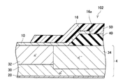
図1に示すように、本実施例のSBD2は、半導体基板4と、上面電極10と、下面電極20と、を有する。
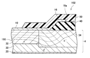
続いて、図3、図4を参照して、第2実施例のSBD102について、第1実施例と異なる点を中心に説明する。図3、図4では、第1実施例のSBD2と同様の要素は図1と同じ符号を用いて示し、詳細な説明を省略する。本実施例のSBD102は、層間絶縁膜40と、フィールドプレート電極16と、保護膜50とをさらに有する点で、第1実施例のSBD2とは異なる。
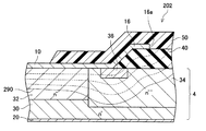
続いて、図5、図6を参照して、第3実施例のSBD202について、第2実施例と異なる点を中心に説明する。図5、図6でも、上記の各実施例のSBD2、102と同様の要素は同じ符号を用いて示し、詳細な説明を省略する。本実施例のSBD202は、低濃度層34内に、絶縁層36がさらに備えられている点が第2実施例のSBD102と異なる。
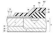
続いて、図7を参照して、第4実施例のSBD302について、第3実施例と異なる点を中心に説明する。図7でも、上記の各実施例のSBD2、102、202と同様の要素は同じ符号を用いて示し、詳細な説明を省略する。本実施例のSBD302では、上面電極10が、ショットキー電極膜12と積層電極膜14とを積層した構造を有する点が第3実施例とは異なる。
4:半導体基板
10:上面電極
12:ショットキー電極膜
14:積層電極膜
16:フィールドプレート電極
16a:端部
20:下面電極
30:高濃度層
32:中濃度層
34:低濃度層
36:絶縁層
40:層間絶縁膜
50:保護膜
90:空乏層
102:SBD
190:空乏層
202:SBD
290:空乏層
302:SBD
Claims (4)
- ダイオードであって、
半導体基板と、
前記半導体基板の上面の一部に接している上面電極と、
前記半導体基板の下面の少なくとも一部に接している下面電極を備えており、
前記半導体基板が、
前記下面電極にオーミック接触するn型の高濃度層と、
前記高濃度層上の一部に形成されており、前記高濃度層よりn型不純物濃度が低いn型の中濃度層と、
前記高濃度層上において前記中濃度層を一巡する範囲に形成されており、前記中濃度層よりn型不純物濃度が低いn型の低濃度層を備えており、
前記上面電極が、前記中濃度層の上面にショットキー接触しており、
前記上面電極と前記半導体基板が接している接触領域が、前記中濃度層を越えて前記低濃度層上に及んでいる、
ダイオード。 - 前記低濃度層内において前記中濃度層を一巡する範囲に形成されている絶縁層をさらに備えており、
前記接触領域の端部が、前記絶縁層上に位置している請求項1に記載のダイオード。 - 前記低濃度層に層間絶縁膜を介して対向するとともに前記上面電極に接続されているフィールドプレート電極をさらに備えており、
前記フィールドプレート電極の前記上面電極と反対側の端部が、前記低濃度層上に位置している、請求項1または2に記載のダイオード。 - 前記層間絶縁膜の比誘電率が、SiO2の比誘電率よりも大きい、請求項3に記載のダイオード。
Priority Applications (3)
| Application Number | Priority Date | Filing Date | Title |
|---|---|---|---|
| JP2016018117A JP2017139293A (ja) | 2016-02-02 | 2016-02-02 | ダイオード |
| US16/072,417 US20190035944A1 (en) | 2016-02-02 | 2017-01-31 | Schottky diode |
| PCT/IB2017/000049 WO2017134508A1 (en) | 2016-02-02 | 2017-01-31 | Schottky diode |
Applications Claiming Priority (1)
| Application Number | Priority Date | Filing Date | Title |
|---|---|---|---|
| JP2016018117A JP2017139293A (ja) | 2016-02-02 | 2016-02-02 | ダイオード |
Publications (2)
| Publication Number | Publication Date |
|---|---|
| JP2017139293A true JP2017139293A (ja) | 2017-08-10 |
| JP2017139293A5 JP2017139293A5 (ja) | 2018-05-17 |
Family
ID=58044102
Family Applications (1)
| Application Number | Title | Priority Date | Filing Date |
|---|---|---|---|
| JP2016018117A Pending JP2017139293A (ja) | 2016-02-02 | 2016-02-02 | ダイオード |
Country Status (3)
| Country | Link |
|---|---|
| US (1) | US20190035944A1 (ja) |
| JP (1) | JP2017139293A (ja) |
| WO (1) | WO2017134508A1 (ja) |
Cited By (1)
| Publication number | Priority date | Publication date | Assignee | Title |
|---|---|---|---|---|
| US10418494B2 (en) | 2017-02-23 | 2019-09-17 | Toyota Jidosha Kabushiki Kaisha | Method of manufacturing semiconductor device |
Families Citing this family (4)
| Publication number | Priority date | Publication date | Assignee | Title |
|---|---|---|---|---|
| JP6560141B2 (ja) * | 2016-02-26 | 2019-08-14 | トヨタ自動車株式会社 | スイッチング素子 |
| JP6560142B2 (ja) * | 2016-02-26 | 2019-08-14 | トヨタ自動車株式会社 | スイッチング素子 |
| JP2018137394A (ja) * | 2017-02-23 | 2018-08-30 | トヨタ自動車株式会社 | 半導体装置の製造方法 |
| CN110265486B (zh) * | 2019-06-20 | 2023-03-24 | 中国电子科技集团公司第十三研究所 | 氧化镓sbd终端结构及制备方法 |
Citations (4)
| Publication number | Priority date | Publication date | Assignee | Title |
|---|---|---|---|---|
| JPS5113580A (en) * | 1974-06-21 | 1976-02-03 | Westinghouse Electric Corp | Shotsutokiibarya daioodo |
| JPS554925A (en) * | 1978-06-26 | 1980-01-14 | Hitachi Ltd | Shot key barrier diode |
| JP2013102081A (ja) * | 2011-11-09 | 2013-05-23 | Tamura Seisakusho Co Ltd | ショットキーバリアダイオード |
| US20130161634A1 (en) * | 2011-12-22 | 2013-06-27 | Epowersoft, Inc. | Method and system for fabricating edge termination structures in gan materials |
Family Cites Families (2)
| Publication number | Priority date | Publication date | Assignee | Title |
|---|---|---|---|---|
| KR20130049919A (ko) * | 2011-11-07 | 2013-05-15 | 현대자동차주식회사 | 실리콘카바이드 쇼트키 배리어 다이오드 소자 및 이의 제조 방법 |
| JP6269276B2 (ja) * | 2014-04-11 | 2018-01-31 | 豊田合成株式会社 | 半導体装置、半導体装置の製造方法 |
-
2016
- 2016-02-02 JP JP2016018117A patent/JP2017139293A/ja active Pending
-
2017
- 2017-01-31 WO PCT/IB2017/000049 patent/WO2017134508A1/en active Application Filing
- 2017-01-31 US US16/072,417 patent/US20190035944A1/en not_active Abandoned
Patent Citations (4)
| Publication number | Priority date | Publication date | Assignee | Title |
|---|---|---|---|---|
| JPS5113580A (en) * | 1974-06-21 | 1976-02-03 | Westinghouse Electric Corp | Shotsutokiibarya daioodo |
| JPS554925A (en) * | 1978-06-26 | 1980-01-14 | Hitachi Ltd | Shot key barrier diode |
| JP2013102081A (ja) * | 2011-11-09 | 2013-05-23 | Tamura Seisakusho Co Ltd | ショットキーバリアダイオード |
| US20130161634A1 (en) * | 2011-12-22 | 2013-06-27 | Epowersoft, Inc. | Method and system for fabricating edge termination structures in gan materials |
Cited By (1)
| Publication number | Priority date | Publication date | Assignee | Title |
|---|---|---|---|---|
| US10418494B2 (en) | 2017-02-23 | 2019-09-17 | Toyota Jidosha Kabushiki Kaisha | Method of manufacturing semiconductor device |
Also Published As
| Publication number | Publication date |
|---|---|
| US20190035944A1 (en) | 2019-01-31 |
| WO2017134508A1 (en) | 2017-08-10 |
Similar Documents
| Publication | Publication Date | Title |
|---|---|---|
| TWI724160B (zh) | 溝槽式金氧半型肖特基二極體 | |
| JP5919033B2 (ja) | ショットキーバリアダイオード | |
| JP2017139293A (ja) | ダイオード | |
| JP2018049951A (ja) | 半導体装置 | |
| JP7012137B2 (ja) | 窒化物半導体装置 | |
| JP2014216410A (ja) | 半導体装置 | |
| JP2006318956A (ja) | ショットキーダイオードを有する半導体装置 | |
| TW201501328A (zh) | 蕭特基二極體結構 | |
| JP5655932B2 (ja) | 半導体装置 | |
| JP2017139289A (ja) | ダイオード | |
| JP2013161918A (ja) | 半導体装置 | |
| JP5547022B2 (ja) | 半導体装置 | |
| JP5406508B2 (ja) | 横型sbd半導体装置 | |
| JP2011009797A (ja) | ショットキーダイオードを有する半導体装置 | |
| JP2016207829A (ja) | 絶縁ゲート型スイッチング素子 | |
| JP7257912B2 (ja) | 半導体装置 | |
| US20110193099A1 (en) | Semiconductor device | |
| JP7147510B2 (ja) | スイッチング素子 | |
| JP2013175607A (ja) | ショットキーバリアダイオード | |
| TWI565084B (zh) | Ditch-type Schottky diodes | |
| JP2011023527A (ja) | 半導体装置 | |
| JP5358141B2 (ja) | 半導体装置 | |
| WO2014155565A1 (ja) | 縦型半導体装置 | |
| JP4322183B2 (ja) | ショットキーバリアダイオード | |
| JP7352151B2 (ja) | スイッチング素子 |
Legal Events
| Date | Code | Title | Description |
|---|---|---|---|
| A521 | Request for written amendment filed |
Free format text: JAPANESE INTERMEDIATE CODE: A523 Effective date: 20180328 |
|
| A621 | Written request for application examination |
Free format text: JAPANESE INTERMEDIATE CODE: A621 Effective date: 20180328 |
|
| A977 | Report on retrieval |
Free format text: JAPANESE INTERMEDIATE CODE: A971007 Effective date: 20190128 |
|
| A131 | Notification of reasons for refusal |
Free format text: JAPANESE INTERMEDIATE CODE: A131 Effective date: 20190205 |
|
| A02 | Decision of refusal |
Free format text: JAPANESE INTERMEDIATE CODE: A02 Effective date: 20190827 |