WO2014141975A1 - ボンディング用ワイヤ - Google Patents
ボンディング用ワイヤ Download PDFInfo
- Publication number
- WO2014141975A1 WO2014141975A1 PCT/JP2014/055669 JP2014055669W WO2014141975A1 WO 2014141975 A1 WO2014141975 A1 WO 2014141975A1 JP 2014055669 W JP2014055669 W JP 2014055669W WO 2014141975 A1 WO2014141975 A1 WO 2014141975A1
- Authority
- WO
- WIPO (PCT)
- Prior art keywords
- wire
- mass
- bonding
- less
- ball
- Prior art date
- Legal status (The legal status is an assumption and is not a legal conclusion. Google has not performed a legal analysis and makes no representation as to the accuracy of the status listed.)
- Ceased
Links
Images


Classifications
-
- H—ELECTRICITY
- H10—SEMICONDUCTOR DEVICES; ELECTRIC SOLID-STATE DEVICES NOT OTHERWISE PROVIDED FOR
- H10W—GENERIC PACKAGES, INTERCONNECTIONS, CONNECTORS OR OTHER CONSTRUCTIONAL DETAILS OF DEVICES COVERED BY CLASS H10
- H10W72/00—Interconnections or connectors in packages
- H10W72/01—Manufacture or treatment
- H10W72/015—Manufacture or treatment of bond wires
-
- C—CHEMISTRY; METALLURGY
- C22—METALLURGY; FERROUS OR NON-FERROUS ALLOYS; TREATMENT OF ALLOYS OR NON-FERROUS METALS
- C22C—ALLOYS
- C22C5/00—Alloys based on noble metals
- C22C5/06—Alloys based on silver
-
- H—ELECTRICITY
- H10—SEMICONDUCTOR DEVICES; ELECTRIC SOLID-STATE DEVICES NOT OTHERWISE PROVIDED FOR
- H10W—GENERIC PACKAGES, INTERCONNECTIONS, CONNECTORS OR OTHER CONSTRUCTIONAL DETAILS OF DEVICES COVERED BY CLASS H10
- H10W72/00—Interconnections or connectors in packages
- H10W72/50—Bond wires
-
- H—ELECTRICITY
- H10—SEMICONDUCTOR DEVICES; ELECTRIC SOLID-STATE DEVICES NOT OTHERWISE PROVIDED FOR
- H10W—GENERIC PACKAGES, INTERCONNECTIONS, CONNECTORS OR OTHER CONSTRUCTIONAL DETAILS OF DEVICES COVERED BY CLASS H10
- H10W72/00—Interconnections or connectors in packages
- H10W72/50—Bond wires
- H10W72/551—Materials of bond wires
- H10W72/555—Materials of bond wires of outermost layers of multilayered bond wires, e.g. material of a coating
-
- C—CHEMISTRY; METALLURGY
- C22—METALLURGY; FERROUS OR NON-FERROUS ALLOYS; TREATMENT OF ALLOYS OR NON-FERROUS METALS
- C22C—ALLOYS
- C22C5/00—Alloys based on noble metals
- C22C5/02—Alloys based on gold
-
- C—CHEMISTRY; METALLURGY
- C22—METALLURGY; FERROUS OR NON-FERROUS ALLOYS; TREATMENT OF ALLOYS OR NON-FERROUS METALS
- C22C—ALLOYS
- C22C9/00—Alloys based on copper
-
- H—ELECTRICITY
- H10—SEMICONDUCTOR DEVICES; ELECTRIC SOLID-STATE DEVICES NOT OTHERWISE PROVIDED FOR
- H10W—GENERIC PACKAGES, INTERCONNECTIONS, CONNECTORS OR OTHER CONSTRUCTIONAL DETAILS OF DEVICES COVERED BY CLASS H10
- H10W72/00—Interconnections or connectors in packages
- H10W72/01—Manufacture or treatment
- H10W72/015—Manufacture or treatment of bond wires
- H10W72/01565—Thermally treating
-
- H—ELECTRICITY
- H10—SEMICONDUCTOR DEVICES; ELECTRIC SOLID-STATE DEVICES NOT OTHERWISE PROVIDED FOR
- H10W—GENERIC PACKAGES, INTERCONNECTIONS, CONNECTORS OR OTHER CONSTRUCTIONAL DETAILS OF DEVICES COVERED BY CLASS H10
- H10W72/00—Interconnections or connectors in packages
- H10W72/071—Connecting or disconnecting
- H10W72/0711—Apparatus therefor
- H10W72/07141—Means for applying energy, e.g. ovens or lasers
-
- H—ELECTRICITY
- H10—SEMICONDUCTOR DEVICES; ELECTRIC SOLID-STATE DEVICES NOT OTHERWISE PROVIDED FOR
- H10W—GENERIC PACKAGES, INTERCONNECTIONS, CONNECTORS OR OTHER CONSTRUCTIONAL DETAILS OF DEVICES COVERED BY CLASS H10
- H10W72/00—Interconnections or connectors in packages
- H10W72/071—Connecting or disconnecting
- H10W72/075—Connecting or disconnecting of bond wires
-
- H—ELECTRICITY
- H10—SEMICONDUCTOR DEVICES; ELECTRIC SOLID-STATE DEVICES NOT OTHERWISE PROVIDED FOR
- H10W—GENERIC PACKAGES, INTERCONNECTIONS, CONNECTORS OR OTHER CONSTRUCTIONAL DETAILS OF DEVICES COVERED BY CLASS H10
- H10W72/00—Interconnections or connectors in packages
- H10W72/071—Connecting or disconnecting
- H10W72/075—Connecting or disconnecting of bond wires
- H10W72/07511—Treating the bonding area before connecting, e.g. by applying flux or cleaning
-
- H—ELECTRICITY
- H10—SEMICONDUCTOR DEVICES; ELECTRIC SOLID-STATE DEVICES NOT OTHERWISE PROVIDED FOR
- H10W—GENERIC PACKAGES, INTERCONNECTIONS, CONNECTORS OR OTHER CONSTRUCTIONAL DETAILS OF DEVICES COVERED BY CLASS H10
- H10W72/00—Interconnections or connectors in packages
- H10W72/071—Connecting or disconnecting
- H10W72/075—Connecting or disconnecting of bond wires
- H10W72/07521—Aligning
-
- H—ELECTRICITY
- H10—SEMICONDUCTOR DEVICES; ELECTRIC SOLID-STATE DEVICES NOT OTHERWISE PROVIDED FOR
- H10W—GENERIC PACKAGES, INTERCONNECTIONS, CONNECTORS OR OTHER CONSTRUCTIONAL DETAILS OF DEVICES COVERED BY CLASS H10
- H10W72/00—Interconnections or connectors in packages
- H10W72/071—Connecting or disconnecting
- H10W72/075—Connecting or disconnecting of bond wires
- H10W72/07531—Techniques
- H10W72/07532—Compression bonding, e.g. thermocompression bonding
- H10W72/07533—Ultrasonic bonding, e.g. thermosonic bonding
-
- H—ELECTRICITY
- H10—SEMICONDUCTOR DEVICES; ELECTRIC SOLID-STATE DEVICES NOT OTHERWISE PROVIDED FOR
- H10W—GENERIC PACKAGES, INTERCONNECTIONS, CONNECTORS OR OTHER CONSTRUCTIONAL DETAILS OF DEVICES COVERED BY CLASS H10
- H10W72/00—Interconnections or connectors in packages
- H10W72/071—Connecting or disconnecting
- H10W72/075—Connecting or disconnecting of bond wires
- H10W72/07551—Connecting or disconnecting of bond wires characterised by changes in properties of the bond wires during the connecting
- H10W72/07554—Connecting or disconnecting of bond wires characterised by changes in properties of the bond wires during the connecting changes in dispositions
-
- H—ELECTRICITY
- H10—SEMICONDUCTOR DEVICES; ELECTRIC SOLID-STATE DEVICES NOT OTHERWISE PROVIDED FOR
- H10W—GENERIC PACKAGES, INTERCONNECTIONS, CONNECTORS OR OTHER CONSTRUCTIONAL DETAILS OF DEVICES COVERED BY CLASS H10
- H10W72/00—Interconnections or connectors in packages
- H10W72/071—Connecting or disconnecting
- H10W72/075—Connecting or disconnecting of bond wires
- H10W72/07551—Connecting or disconnecting of bond wires characterised by changes in properties of the bond wires during the connecting
- H10W72/07555—Connecting or disconnecting of bond wires characterised by changes in properties of the bond wires during the connecting changes in materials
-
- H—ELECTRICITY
- H10—SEMICONDUCTOR DEVICES; ELECTRIC SOLID-STATE DEVICES NOT OTHERWISE PROVIDED FOR
- H10W—GENERIC PACKAGES, INTERCONNECTIONS, CONNECTORS OR OTHER CONSTRUCTIONAL DETAILS OF DEVICES COVERED BY CLASS H10
- H10W72/00—Interconnections or connectors in packages
- H10W72/50—Bond wires
- H10W72/521—Structures or relative sizes of bond wires
- H10W72/522—Multilayered bond wires, e.g. having a coating concentric around a core
-
- H—ELECTRICITY
- H10—SEMICONDUCTOR DEVICES; ELECTRIC SOLID-STATE DEVICES NOT OTHERWISE PROVIDED FOR
- H10W—GENERIC PACKAGES, INTERCONNECTIONS, CONNECTORS OR OTHER CONSTRUCTIONAL DETAILS OF DEVICES COVERED BY CLASS H10
- H10W72/00—Interconnections or connectors in packages
- H10W72/50—Bond wires
- H10W72/531—Shapes of wire connectors
- H10W72/536—Shapes of wire connectors the connected ends being ball-shaped
-
- H—ELECTRICITY
- H10—SEMICONDUCTOR DEVICES; ELECTRIC SOLID-STATE DEVICES NOT OTHERWISE PROVIDED FOR
- H10W—GENERIC PACKAGES, INTERCONNECTIONS, CONNECTORS OR OTHER CONSTRUCTIONAL DETAILS OF DEVICES COVERED BY CLASS H10
- H10W72/00—Interconnections or connectors in packages
- H10W72/50—Bond wires
- H10W72/531—Shapes of wire connectors
- H10W72/5363—Shapes of wire connectors the connected ends being wedge-shaped
-
- H—ELECTRICITY
- H10—SEMICONDUCTOR DEVICES; ELECTRIC SOLID-STATE DEVICES NOT OTHERWISE PROVIDED FOR
- H10W—GENERIC PACKAGES, INTERCONNECTIONS, CONNECTORS OR OTHER CONSTRUCTIONAL DETAILS OF DEVICES COVERED BY CLASS H10
- H10W72/00—Interconnections or connectors in packages
- H10W72/50—Bond wires
- H10W72/541—Dispositions of bond wires
- H10W72/5434—Dispositions of bond wires the connected ends being on auxiliary connecting means on bond pads, e.g. on other bond wires
-
- H—ELECTRICITY
- H10—SEMICONDUCTOR DEVICES; ELECTRIC SOLID-STATE DEVICES NOT OTHERWISE PROVIDED FOR
- H10W—GENERIC PACKAGES, INTERCONNECTIONS, CONNECTORS OR OTHER CONSTRUCTIONAL DETAILS OF DEVICES COVERED BY CLASS H10
- H10W72/00—Interconnections or connectors in packages
- H10W72/50—Bond wires
- H10W72/541—Dispositions of bond wires
- H10W72/5449—Dispositions of bond wires not being orthogonal to a side surface of the chip, e.g. fan-out arrangements
-
- H—ELECTRICITY
- H10—SEMICONDUCTOR DEVICES; ELECTRIC SOLID-STATE DEVICES NOT OTHERWISE PROVIDED FOR
- H10W—GENERIC PACKAGES, INTERCONNECTIONS, CONNECTORS OR OTHER CONSTRUCTIONAL DETAILS OF DEVICES COVERED BY CLASS H10
- H10W72/00—Interconnections or connectors in packages
- H10W72/50—Bond wires
- H10W72/541—Dispositions of bond wires
- H10W72/547—Dispositions of multiple bond wires
-
- H—ELECTRICITY
- H10—SEMICONDUCTOR DEVICES; ELECTRIC SOLID-STATE DEVICES NOT OTHERWISE PROVIDED FOR
- H10W—GENERIC PACKAGES, INTERCONNECTIONS, CONNECTORS OR OTHER CONSTRUCTIONAL DETAILS OF DEVICES COVERED BY CLASS H10
- H10W72/00—Interconnections or connectors in packages
- H10W72/50—Bond wires
- H10W72/551—Materials of bond wires
-
- H—ELECTRICITY
- H10—SEMICONDUCTOR DEVICES; ELECTRIC SOLID-STATE DEVICES NOT OTHERWISE PROVIDED FOR
- H10W—GENERIC PACKAGES, INTERCONNECTIONS, CONNECTORS OR OTHER CONSTRUCTIONAL DETAILS OF DEVICES COVERED BY CLASS H10
- H10W72/00—Interconnections or connectors in packages
- H10W72/50—Bond wires
- H10W72/551—Materials of bond wires
- H10W72/552—Materials of bond wires comprising metals or metalloids, e.g. silver
-
- H—ELECTRICITY
- H10—SEMICONDUCTOR DEVICES; ELECTRIC SOLID-STATE DEVICES NOT OTHERWISE PROVIDED FOR
- H10W—GENERIC PACKAGES, INTERCONNECTIONS, CONNECTORS OR OTHER CONSTRUCTIONAL DETAILS OF DEVICES COVERED BY CLASS H10
- H10W72/00—Interconnections or connectors in packages
- H10W72/50—Bond wires
- H10W72/551—Materials of bond wires
- H10W72/552—Materials of bond wires comprising metals or metalloids, e.g. silver
- H10W72/5522—Materials of bond wires comprising metals or metalloids, e.g. silver comprising gold [Au]
-
- H—ELECTRICITY
- H10—SEMICONDUCTOR DEVICES; ELECTRIC SOLID-STATE DEVICES NOT OTHERWISE PROVIDED FOR
- H10W—GENERIC PACKAGES, INTERCONNECTIONS, CONNECTORS OR OTHER CONSTRUCTIONAL DETAILS OF DEVICES COVERED BY CLASS H10
- H10W72/00—Interconnections or connectors in packages
- H10W72/851—Dispositions of multiple connectors or interconnections
- H10W72/874—On different surfaces
- H10W72/884—Die-attach connectors and bond wires
-
- H—ELECTRICITY
- H10—SEMICONDUCTOR DEVICES; ELECTRIC SOLID-STATE DEVICES NOT OTHERWISE PROVIDED FOR
- H10W—GENERIC PACKAGES, INTERCONNECTIONS, CONNECTORS OR OTHER CONSTRUCTIONAL DETAILS OF DEVICES COVERED BY CLASS H10
- H10W72/00—Interconnections or connectors in packages
- H10W72/90—Bond pads, in general
- H10W72/951—Materials of bond pads
- H10W72/952—Materials of bond pads comprising metals or metalloids, e.g. PbSn, Ag or Cu
-
- H—ELECTRICITY
- H10—SEMICONDUCTOR DEVICES; ELECTRIC SOLID-STATE DEVICES NOT OTHERWISE PROVIDED FOR
- H10W—GENERIC PACKAGES, INTERCONNECTIONS, CONNECTORS OR OTHER CONSTRUCTIONAL DETAILS OF DEVICES COVERED BY CLASS H10
- H10W74/00—Encapsulations, e.g. protective coatings
-
- H—ELECTRICITY
- H10—SEMICONDUCTOR DEVICES; ELECTRIC SOLID-STATE DEVICES NOT OTHERWISE PROVIDED FOR
- H10W—GENERIC PACKAGES, INTERCONNECTIONS, CONNECTORS OR OTHER CONSTRUCTIONAL DETAILS OF DEVICES COVERED BY CLASS H10
- H10W90/00—Package configurations
- H10W90/701—Package configurations characterised by the relative positions of pads or connectors relative to package parts
- H10W90/731—Package configurations characterised by the relative positions of pads or connectors relative to package parts of die-attach connectors
- H10W90/734—Package configurations characterised by the relative positions of pads or connectors relative to package parts of die-attach connectors between a chip and a stacked insulating package substrate, interposer or RDL
-
- H—ELECTRICITY
- H10—SEMICONDUCTOR DEVICES; ELECTRIC SOLID-STATE DEVICES NOT OTHERWISE PROVIDED FOR
- H10W—GENERIC PACKAGES, INTERCONNECTIONS, CONNECTORS OR OTHER CONSTRUCTIONAL DETAILS OF DEVICES COVERED BY CLASS H10
- H10W90/00—Package configurations
- H10W90/701—Package configurations characterised by the relative positions of pads or connectors relative to package parts
- H10W90/731—Package configurations characterised by the relative positions of pads or connectors relative to package parts of die-attach connectors
- H10W90/736—Package configurations characterised by the relative positions of pads or connectors relative to package parts of die-attach connectors between a chip and a stacked lead frame, conducting package substrate or heat sink
-
- H—ELECTRICITY
- H10—SEMICONDUCTOR DEVICES; ELECTRIC SOLID-STATE DEVICES NOT OTHERWISE PROVIDED FOR
- H10W—GENERIC PACKAGES, INTERCONNECTIONS, CONNECTORS OR OTHER CONSTRUCTIONAL DETAILS OF DEVICES COVERED BY CLASS H10
- H10W90/00—Package configurations
- H10W90/701—Package configurations characterised by the relative positions of pads or connectors relative to package parts
- H10W90/751—Package configurations characterised by the relative positions of pads or connectors relative to package parts of bond wires
- H10W90/754—Package configurations characterised by the relative positions of pads or connectors relative to package parts of bond wires between a chip and a stacked insulating package substrate, interposer or RDL
-
- H—ELECTRICITY
- H10—SEMICONDUCTOR DEVICES; ELECTRIC SOLID-STATE DEVICES NOT OTHERWISE PROVIDED FOR
- H10W—GENERIC PACKAGES, INTERCONNECTIONS, CONNECTORS OR OTHER CONSTRUCTIONAL DETAILS OF DEVICES COVERED BY CLASS H10
- H10W90/00—Package configurations
- H10W90/701—Package configurations characterised by the relative positions of pads or connectors relative to package parts
- H10W90/751—Package configurations characterised by the relative positions of pads or connectors relative to package parts of bond wires
- H10W90/756—Package configurations characterised by the relative positions of pads or connectors relative to package parts of bond wires between a chip and a stacked lead frame, conducting package substrate or heat sink
Definitions
- the present invention relates to electrodes on a semiconductor element or electrodes and a lead frame in a semiconductor package such as a power IC, LSI, transistor, BGA (Ball (Grid package), QFN (Quad Flat Non lead package), LED (light emitting diode), etc.
- the present invention relates to a bonding wire for connecting a conductor wiring of a circuit wiring board such as a ceramic substrate or a printed board by a combination of a ball bonding method and a stud bump method.
- a package substrate 3 is provided on a wiring board 1 via solder balls 2, and a semiconductor element is further provided on the package substrate 3 via a die bonding material 4.
- a (chip) 5 is provided and the semiconductor element 5 is sealed with a sealing material 6. Ball bonding is usually used for electrical connection between the electrode a of the semiconductor element 5 and the conductor wiring (terminal) c of the package substrate 3 in this semiconductor package.
- a stud bump is provided on one electrode a and the first electrode is connected to the other electrode a. After that, stitch bonding is performed on the electrode a provided with the stud bump. Further, in the electrical connection between the electrode a and the conductor wiring (terminal) c of the package substrate 3, after the bonding is performed by the ball bonding method, a stud bump is provided on the stitch bond portion in order to increase the bonding reliability. Is performed (security bond).
- a 1st bond may be formed on the conductor wiring (terminal) c of the package substrate 3 and stitch bonding may be performed on the electrode a. Stud bumps are formed in advance, and stitch bonding is performed on them (reverse bonding).
- the electrical connection between the electrode a of the semiconductor element 5 and the conductor wiring (terminal) c of the package substrate 3 in the semiconductor package may be performed by a combination of the ball bonding method and the stud bump method.
- the LED 15 is provided on the case heat sink 11 via the die bonding material 12, and the phosphor e is mixed.
- the LED 15 is sealed by the material 14.
- the electrical connection between the electrode a of the LED 15 and the conductor wiring (terminal) c of the case electrode 13 constituting the circuit wiring board is performed by a combination of the ball bonding method and the stud bump method as in the case of a semiconductor package such as BGA.
- 16 is a resin case body.
- Stud bumps in the above-described stud bump method are formed, for example, as shown in FIGS. That is, from the state where the wire W is inserted into the capillary 10a and a ball (FAB: Free Air Ball) b is formed at the tip thereof, the clamp 10b is opened and the capillary 10a is lowered toward the electrode a on the integrated circuit element. To do. At this time, the ball (FAB) b is captured in the capillary 10a.
- FAB Free Air Ball
- the capillary 10a grips the molten ball b and applies heat / load / ultrasonic waves to the molten ball b, whereby the molten ball b Is crimped (formed as a crimped ball b ′) and solid-phase bonded to the electrode a (FIG. 5 (b)), the clamp 10b is opened and the capillary 10a is slightly raised.
- the wire W is cut from the press-bonded ball b ′ by the action of the capillary 10a (FIGS. (C) to (f)), and the press-bonded ball b ′ thus formed is called a stud bump.
- a connection method in which the stud bump b ′ is combined with the ball bonding method is, for example, in reverse bonding, after passing through the modes shown in FIGS. 3A to 3F, the capillary 10a as shown in FIG. After rising to a certain height, the tip of the wire W secured at the tip of the capillary 10a is discharged (sparked) by applying a high voltage with the discharge rod g, and the heat melts the wire W. The melted wire material is solidified into a spherical ball b by the surface tension (FIG. 5 (g)). Next, as shown in FIG.
- the capillary 10a gripping the molten ball b moves to the position immediately above the conductor wiring c, and then descends toward the conductor wiring c and is pressed (see FIG. At the same time, heat, load, and ultrasonic waves are applied to the pressed portion, whereby the molten ball b is pressure-bonded (formed as a pressure-bonded ball b ′) and solid-phase bonded to the conductor wiring c, and then the clamp 10b. (J (j) to (k) in the figure) while opening and rising, the capillaries 10a are caused to move specially to form a stable loop. There is a case where an operation of adding a “fist” is made (see the solid line from the chain line in FIG. 5K).
- Capillary 10a that reaches directly above stud bump b 'formed on electrode a descends toward stud bump b' and presses wire W against stud bump (2nd target) b '. At the same time, heat, a load, and an ultrasonic wave are applied to the pressing portion, thereby deforming the wire W, and stitches for joining the wire W to the stud bump b ′ and a tail for securing the tail in the next step. A bond is formed (2nd junction, (l) to (m) in the figure).
- the capillary 10a rises with the wire W remaining, and after securing a tail of a certain length at the tip of the capillary 10a, the clamp 10b is closed (by grabbing the wire W), and the tail The wire W is torn off from the bond portion ((m) to (n) in the figure).
- the capillary 10a stops when it rises to the required height, and the tip of the wire W secured at the tip of the capillary 10a is discharged (sparked) by applying a high voltage with the discharge rod g, and the wire is heated by the heat. W is melted, and the melted wire material becomes a spherical ball b which is nearly spherical due to the surface tension, and is solidified ((o) in the figure).
- the above cycle is the case of the stud bump method-ball bonding method, and the ball bonding is performed after the stud bump b 'is formed.
- the ball bonding method-stud bump method when the security bond is applied, one cycle is performed.
- the order in the cycle is different, and the formation of the stud bump b ′ is later in FIG. That is, after the operations of (h) to (o) in FIG. 3 are first performed on the electrode a as shown in FIGS. 4 (a) to (h), the operations in FIGS. 3 (a) to (g) are performed.
- the operation is performed on the conductor wiring c which is stitch-bonded as shown in FIGS.
- gold of 4N (purity: 99.99 mass% or more) to 2N is used as the material of the bonding wire (wire) W to be bonded by combining this ball bonding method and the stud bump method.
- Gold is used in this way because gold does not oxidize even when exposed to heat in the atmosphere. Therefore, both when forming stud bumps on stitch bonds and when making stitch bonds on stud bumps. This is because there is no particular influence.
- gold can easily cut the wire when forming the stud bump, and the production is stabilized.
- Gold bonding wires are expensive.
- the copper bonding wire that is an alternative material is inexpensive, but the FAB is harder than the gold bonding wire, and if the tip of the electrode a is fragile, the risk of chip damage increases.
- the 2nd bondability is poor as compared with the gold bonding wire, and there is a problem in the continuous bonding property.
- Pd-coated copper bonding wires have better 2nd bondability and better continuous bondability than copper bonding wires, but FAB is harder than copper bonding wires, and there is a problem of chip damage.
- the LED 15 of the electrode a coated with Au is used, and a gold bonding wire is used for connection with the electrode a. Since this gold combination cannot reduce the cost, an inexpensive bonding wire is also desired for the LED 15.
- the copper bonding wire has difficulty in continuous bonding, and the Pd-coated copper bonding wire has a hard FAB, which may cause chip damage.
- the reflectance of the bonding wire itself is low, and the wire portion becomes a shadow. Therefore, depending on the type of the LED 15, the brightness of the LED 15 itself may be lowered.
- the stitch bonding when a copper bonding wire or a Pd-coated copper bonding wire is used, when the stitch bonding is performed after the stud bump b ′ is formed, the stud bump b ′ is oxidized before the stitch bonding is performed, and the stitch bond is Can't be stable.
- the stitch bond portion is oxidized before the stud bump is performed after the stitch bond, so that the stud bump cannot be stably bonded.
- Patent Document 4 in order to improve wire strength and heat resistance, Ca (calcium), Sr (strontium), Y (yttrium), La (lanthanum), Ce (cerium), Eu (europium), Be ( Although it is described that beryllium), Ge (germanium), In (indium), and Sn (tin) are added, if these elements are added in a large amount, the hardness of the ball b is increased and the electrode a is damaged. There's a problem.
- Patent Document 4 Pt (platinum), Pd, Cu, Ru (ruthenium), Os (osmium), Rh (rhodium), Ir (iridium), and Au are added in order to increase the bonding reliability of the wire. It is described. However, if such an element is added in a large amount, the electric resistance of the wire itself is increased, resulting in a problem that the performance as the bonding wire W is impaired. That is, as described above, in a semiconductor package such as a BGA, the electrodes a are smaller and the distance between the electrodes a is closer, so that it is required to reduce the first junction.
- the wire W is cut by the operation of the capillary 10a (see FIGS. 3D and 3E), but the difference in the size of the crystal grains immediately above the wire W and the molten ball b is different. If there is, this cutting can be performed stably. That is, the tip of the wire W is discharged (sparked) by applying a high voltage with the discharge rod g, and when the wire W is melted by the heat to form the molten ball b, the wire W portion immediately above the molten ball b is Although affected by heat, if the crystal grain of the wire W itself is large, the crystal grain coarsening due to the thermal effect does not progress and there is no difference in crystal grains. On the other hand, if the crystal grains of the wire W itself are fine, cutting easily occurs at the boundary between the portion where the crystal grains are coarsened due to the thermal effect and the fine portion.
- Patent Document 5 states that “a ternary alloy-based bonding wire made of Ag, Au, and Pd, gold (Au) being 4 to 10% by mass, palladium (Pd) being 2 to 5% by mass, an oxidizing non-noble metal. There is a description regarding a “bonding wire in which the additive element is 15 to 70 ppm by mass and the balance is silver (Ag)”. However, the bonding wire as described in this document does not consider the cutting ability at the time of manufacturing the stud bump as described above, and there is a concern that the shape of the stud bump varies and a machine stop occurs.
- the object of the present invention is to provide a silver bonding wire that can be connected by a combination of a ball bonding method and a stud bump method, which is cheaper and more stable than a gold bonding wire under the above circumstances.
- the present invention provides a bonding wire that is connected by a combination of a ball bonding method and a stud bump method, mainly composed of Ag, and an additive amount of Au of 0.9 mass% or more and 5.0 mass%.
- the addition amount of Pd is 0.1% by mass or more and 5.0% by mass or less
- the total addition amount of Au and Pd is 1.0% by mass or more and 8.0% by mass or less
- the wire (W) The ratio of 0.2% proof stress (YS) and tensile strength (TS) at room temperature (100 ⁇ YS / TS) is 80% or more, preferably 90% or more.
- one or more elements selected from Ca and rare earth elements can be contained in a total of 20 ppm by mass to 500 ppm by mass, and one or more elements selected from Cu and Ni can be added in a total of 1000 ppm.
- the specific resistance of the wire can be 5.0 ⁇ ⁇ cm or less, preferably 3.0 ⁇ ⁇ cm or less.
- the bonding wire mainly composed of Ag can be made cheaper than the gold bonding wire mainly composed of Au.
- the molten ball b formed at the tip of the wire W melted by the spark by the discharge rod g becomes unstable, and it is difficult to stably obtain a FAB having a high sphericity.
- the molten ball b becomes stable and an FAB having a high sphericity can be obtained.
- the addition amount of Au exceeds 5.0 mass%, a wire will become expensive. From this point, the amount of Au added is preferably 2.6% by mass or less.
- Pd is added to obtain the corrosion resistance of the first joint.
- an electrode a of a semiconductor package such as a BGA is coated with aluminum or an aluminum alloy.
- the electrode a of the LED is often coated with gold, but a coating material of aluminum or aluminum alloy may be used.
- an intermetallic compound layer of silver and aluminum is formed at the bonding interface.
- Ag 2 Al grows in this compound layer, the corrosion resistance in a wet environment deteriorates.
- 0.1 mass% or more of Pd is added to the Ag wire, a Pd enriched layer is formed on the outer peripheral portion of the FAB, thereby suppressing generation of Ag 2 Al.
- the addition amount of Pd exceeds 5.0 mass%, FAB becomes hard and defects such as cracks occur in the electrode a.
- the addition of Pd and Au alone is also effective, but the melting point of the wire is higher when the same amount of Pd and Au is added as a sum of Pd and Au than when a certain amount of Pd or Au is added.
- the wire to which Pd and Au are added in combination has higher heat resistance. Therefore, the total amount of Pd and Au added is 1.0% by mass or more and 8.0% by mass or less. When the total amount of Pd and Au added exceeds 8.0% by mass, the electrical resistance of the wire increases. Further, the hardness of the ball b is increased, and the electrode a is damaged at the time of the first bonding. Furthermore, if the total amount of addition is less than 3.0% by mass, the electric resistance of the wire becomes close to that of a gold wire, so that the wire diameter can be reduced.
- the specific resistance of the wire exceeds 3.0 ⁇ ⁇ cm and is 5.0 ⁇ ⁇ cm or less, there is no problem because the required electrical characteristics can be obtained by increasing the wire diameter, but 3.0 ⁇ If it is cm or less, it is equal to or less than the specific resistance of the 2N (99%) Au wire, so that the 2NAu wire can be easily replaced or replaced.
- Ca and rare earth elements are added in order to improve wire strength and heat resistance.
- the content is less than 20 ppm by mass, the heat resistance of the wire is lowered, causing a practical problem.
- the total addition amount of Ca and rare earth elements is 20 mass ppm or more and 500 mass ppm or less. More preferably, it is 20 mass ppm or more and 100 mass ppm or less, and if it is this range, the heat resistance of a wire is high and the damage degree of the electrode a at the time of 1st joining can also be restrained lower.
- addition of Ca is most preferable.
- addition of a trace amount is effective in improving the heat resistance and strength of the wire.
- the total addition amount of Cu and Ni is preferably 1000 ppm to 10000 ppm by mass.
- the wire diameter of the wire W is arbitrary as long as it can be used as a bonding wire, and is, for example, 12 ⁇ m or more and 50.8 ⁇ m or less. If it is 50.8 ⁇ m or less, the molten ball b can be made smaller, and if it is less than 12 ⁇ m, it becomes difficult for an operator to pass the wire W through the capillary 10a before bonding, workability is deteriorated, and air pressure is applied to the wire by air pressure. Sufficient tension cannot be applied, and loop control may be difficult.
- Various methods can be used as the method for manufacturing the bonding wire W described above. For example, 0.9 mass% or more and 5.0 mass% or less of Au and 0.1% of Pd in 0.19 mass% or more of Ag. From 1.0% to 8.0% by mass in total of Pd and Au, 20% to 500% by mass in total of one or more elements selected from Ca and rare earth, One or more elements selected from Cu and Ni are added in a total of 1000 to 10000 mass ppm, and a rod having the chemical composition with a large wire diameter is manufactured by a continuous casting method, and the wire diameter is sequentially penetrated to a die of 50.8 ⁇ m or less. By drawing the wire, the wire is drawn to a predetermined wire diameter. Thereafter, the wire W is subjected to a tempering heat treatment.
- the tempering heat treatment is a continuous heat treatment by drawing the wire W to a predetermined wire diameter and winding the wire W around the reel, running it in a tubular heat treatment furnace, and winding it again with a take-up reel. .
- the YS and TS of the bonding wire W were calculated by performing a tensile test on a sample having a length of 100 mm at room temperature of 15 to 25 ° C. That is, in the tensile test, the value obtained by dividing the maximum load until breakage by the initial cross-sectional area is the value obtained by dividing the load when the permanent strain of TS: 0.2% remains by the initial cross-sectional area (permanent at unloading) YS is the stress at which the strain becomes 0.2%.
- the wire W before the tempering heat treatment has a deformed structure in which the processing strain at the time of wire drawing remains, and the crystal structure is fine.
- the 100 ⁇ YS / TS of such a deformed structure is almost 100%, but when subjected to a tempering heat treatment at a low temperature or for a short time, a “recovery” occurs in which the processing strain is gradually released, and the heat treatment temperature is higher.
- a tempering heat treatment is applied for a long time, the processing strain is further released, and “recrystallization” occurs in which the crystal grains become large, and YS gradually decreases with respect to TS (100 ⁇ YS / TS is small). Become).
- this 100 ⁇ YS / TS is less than 80%, most of the wire is recrystallized and the crystal structure becomes large, but if it is 80% or more, the recrystallization stays in a part of the wire and some of the crystal grains are also present. It is about to become large. Furthermore, when it is 90% or more, most of the crystal grains have a deformed structure that remains fine.
- the wire is cut from the press-bonded ball by various actions of the capillary, but if there is a boundary of the crystal structure of the wire, it can be easily cut at that portion. That is, if there are fine crystal grain portions and coarse crystal grain portions, breakage tends to occur at the boundary portion.
- HAZ Heat Affect Zone
- the 100 ⁇ YS / TS of the wire is 80% or more and the crystal grains are fine, a boundary between the crystal grains is formed by the HAZ and the wire, and cutting at the time of the stud bump occurs easily. Furthermore, if it is 90% or more, the boundary of a crystal grain will become clearer and a cutting
- the present invention is mainly composed of Ag as described above, it can be made cheaper than gold bonding wires, and addition of appropriate amounts of Pd, Au, Ca, rare earth elements, Cu, Ni and room temperature elongation. Thus, the connection by the combination of the ball bonding method and the stud bump method can be stably performed.
- a silver alloy having chemical components shown in Table 1 was cast to prepare an 8 mm ⁇ wire rod.
- the wire rod was drawn into a silver alloy wire having a predetermined final wire diameter (25 ⁇ m ⁇ ), and was continuously annealed at various heating temperatures and heating times.
- the chemical components were quantified by ICP-OES (high frequency inductively coupled plasma emission spectroscopy).
- Each of the continuously annealed wires W was subjected to a tensile test at room temperature of 15 to 25 ° C. to measure 0.2% proof stress (YS) and tensile strength (TS).
- YS proof stress
- TS tensile strength
- Table 2 shows the continuous bump property, chip damage of the stud bump portion, electrical resistance, wire flow during resin sealing, and comprehensive evaluation in the bonding sample used for the evaluation. Their evaluation methods are as follows.
- Electrode resistance The electric resistance at room temperature was measured using a four-terminal method. If the average of the specific resistance of the three samples is 3.0 ⁇ ⁇ cm or less, there is little change in electrical characteristics when replacing the gold wire, so “A” should be more than 3.0 ⁇ ⁇ cm and 5.0 ⁇ ⁇ cm or less. Since there are few practical problems in replacement from gold wire, “B” is considered to be unsuitable for replacement from gold wire if it exceeds 5.0 ⁇ ⁇ cm.
- FAB sphericity 100 FABs each having a diameter twice as large as each wire diameter were produced with a wire bonder, and the diameter in a direction perpendicular to the direction parallel to the FAB wire was measured. If the difference between the diameters is 2 ⁇ m or less, it is considered to be close to a true sphere, and “A” is considered to be close to a true sphere.
- HAST Corrosion Resistance Evaluation
- the “wire flow at the time of resin sealing” is “D” in Comparative Examples 1 and 6, while the Comparative Example 7 is Au
- the total amount of addition of Pd and Pd is less than 1.0 mass%, one or more elements selected from Ca and rare earth elements described later are added in a total of 350 mass ppm. “Wire flow” is “B”.
- the “electric resistance” becomes “D” from Comparative Examples 5 and 8.
- the “continuous bump property” is “D” from Comparative Examples 2, 3, and 8 to 10. Become.
- the addition amount of Au according to the present invention is 0.9 mass% to 5.0 mass%
- the addition amount of Pd is 0.1 mass% to 5.0 mass%
- the addition of Au and Pd In prototype examples 1 to 15 in which the total amount is 1.0% by mass or more and 8% by mass or less, and the ratio between the 0.2% proof stress and the tensile strength of the wire W is 80% or more, “continuous” In “Bump property”, “Chip damage just below stud bump part”, “Wire flow during resin sealing”, “Replacement from Au wire”, “FAB sphericity”, “HAST” and “Comprehensive evaluation” It can be understood that it is either “A” or “B” and can be used practically without any trouble.
- the ratio of the 0.2% proof stress to the tensile strength of the wire W is 80% or more, from the prototype examples 1 to 15 and the comparative examples 1, 4 to 7, 11, and 12, the continuous bump property “A ”Or“ B ”, but if it is 90% or more, it becomes“ A ”in the continuous bump property from the prototype examples 2, 3, 6 to 8, 11 to 13, 15 and the comparative example 5, and is more excellent.
- the addition amount of Au is 0.9 mass% or more and 2.6 mass% or less
- the addition amount of Pd is 0.1 mass% or more and 1.5 mass% or less
- the total addition amount of Au and Pd is 1.
- the ratio between the 0.2% proof stress and the tensile strength of the wire W is 90% or more, and the added amount of Au: 0.9 mass% or more 2.6. Mass% or less, Pd addition amount: 0.1 mass% or more and 1.5 mass% or less, and total addition amount of Au and Pd: 1.0 mass% or more and 3.0 mass% or less, from Ca and rare earth elements
- Circuit wiring board (case electrode) 5 Semiconductor element 15 LED W Wire for bonding a Electrode b of semiconductor element (LED) Molten ball b 'Crimp ball (stud bump) c Conductor wiring (lead terminal) of circuit wiring board
Landscapes
- Chemical & Material Sciences (AREA)
- Engineering & Computer Science (AREA)
- Materials Engineering (AREA)
- Mechanical Engineering (AREA)
- Metallurgy (AREA)
- Organic Chemistry (AREA)
- Wire Bonding (AREA)
Abstract
金ボンディングワイヤより安価でかつ安定してボールボンディング法とスタッドバンプ法の組み合わせによる接続が可能な銀ボンディング用ワイヤとする。Agを主成分とし、Auの添加量を0.9質量%以上2.6質量%以下、Pdの添加量を0.1質量%以上1.5質量%以下、かつAuとPdの添加量の合計を1.0質量%以上3.0質量%以下、かつAuとPdの添加量の合計を1.0質量%以上3.0質量%以下、Ca、希土類元素から選ばれる1種以上の元素を合計で20質量ppm以上、500質量ppm以下、Cu、Niから選ばれる1種以上の元素を合計で1000質量ppm以上10000質量ppm以下のワイヤWである。そのワイヤWの0.2%耐力と同引張強さとの比が90%以上、同固有抵抗は3.0μΩ・cm以下である。
Description
この発明は、パワーIC、LSI、トランジスタ、BGA(Ball Grid Array package)、QFN(Quad Flat Non lead package)、LED(発光ダイオード)等の半導体パッケージにおける半導体素子上の電極同士もしくは電極とリードフレーム、セラミック基板、プリント基板等の回路配線基板の導体配線とをボールボンディング法およびスタッドバンプ法の組み合わせによって接続するためのボンディング用ワイヤに関するものである。
上記BGA等の半導体パッケージは、例えば、図1に示すように、配線板1上にはんだボール2を介してパッケージ基板3を設け、さらに、そのパッケージ基板3にダイボンディング材4を介して半導体素子(チップ)5を設けて、その半導体素子5を封止材6によって封止した構造である。この半導体パッケージにおける半導体素子5の電極aとパッケージ基板3の導体配線(端子)cとの電気接続では通常はボールボンディング法が用いられる。
しかし、電極a同士を接続する必要がある場合、電極aに直接ステッチボンドすると電極aが破壊される恐れがあるため、一方の電極a上にスタッドバンプを設け、他方の電極aに1st接合のあとスタッドバンプが設けられた電極a上にステッチボンドを行う。
また、電極aとパッケージ基板3の導体配線(端子)cとの電気接続では、ボールボンディング法によって接合が行われた後、接合信頼性を高めるためにステッチボンド部の上にスタッドバンプを設けることが行われる(セキュリティボンド)。
さらに、半導体パッケージの低背化のために、パッケージ基板3の導体配線(端子)cに1stボンドを形成し、電極aにステッチボンドを行うこともなされるが、その場合、事前に電極aにスタッドバンプを形成しておき、その上にステッチボンドを行う(逆ボンド)。
このように、半導体パッケージにおける半導体素子5の電極aとパッケージ基板3の導体配線(端子)cとの電気接続ではボールボンディング法とスタッドバンプ法の組み合わせで接合が行われることがある。
また、電極aとパッケージ基板3の導体配線(端子)cとの電気接続では、ボールボンディング法によって接合が行われた後、接合信頼性を高めるためにステッチボンド部の上にスタッドバンプを設けることが行われる(セキュリティボンド)。
さらに、半導体パッケージの低背化のために、パッケージ基板3の導体配線(端子)cに1stボンドを形成し、電極aにステッチボンドを行うこともなされるが、その場合、事前に電極aにスタッドバンプを形成しておき、その上にステッチボンドを行う(逆ボンド)。
このように、半導体パッケージにおける半導体素子5の電極aとパッケージ基板3の導体配線(端子)cとの電気接続ではボールボンディング法とスタッドバンプ法の組み合わせで接合が行われることがある。
また、上記半導体素子の一つであるLEDのパッケージにおいては、例えば、図2に示すように、ケースヒートシンク11にダイボンディング材12を介してLED15を設けて、蛍光体eを混ぜ合わせた封止材14によってLED15を封止した構造である。このパッケージにおけるLED15の電極aと回路配線基板をなすケース電極13の導体配線(端子)cとの電気接続は、BGA等の半導体パッケージと同様に上記ボールボンディング法とスタッドバンプ法の組み合わせによって行われる。図中、16は樹脂製ケースボディである。
上記のスタッドバンプ法におけるスタッドバンプは、例えば、図3(a)~(f)に示すようにして形成される。すなわち、ワイヤWがキャピラリー10aに挿通されてその先端にボール(FAB:Free Air Ball)bが形成された状態から、クランプ10bが開いて、キャピラリー10aが集積回路素子上の電極aに向かって降下する。このとき、ボール(FAB)bはキャピラリー10a内に捕捉される。
ターゲットである電極aに溶融ボールbが接触すると(キャピラリー10aが電極aに至ると)キャピラリー10aが溶融ボールbをグリップし、溶融ボールbに熱・荷重・超音波を与え、それによって溶融ボールbが圧着されて(圧着ボールb’となって)電極aと固相接合された後(同図(b)、クランプ10bが開いてわずかにキャピラリー10aが上昇する。その後、クランプ10bが閉じ、様々なキャピラリー10aの動作によってワイヤWが圧着ボールb’から切断される(同図(c)~(f))。このようにしてできた圧着ボールb’のことをスタッドバンプという。
このスタッドバンプb’をボールボンディング法に組み合わせた接続方法は、例えば、逆ボンドでは、図3(a)~(f)に示す態様を経た後、同図(g)に示すように、キャピラリー10aは、一定高さまで上昇した後、そのキャピラリー10aの先端に確保されたワイヤWの先端部分に、放電棒gでもって高電圧を掛けて放電し(スパークし)、その熱でワイヤWを溶かし、この溶けたワイヤ素材は表面張力によって球状に近い溶融ボールbになって固まる(同図(g))。
つぎに、同図(h)に示すように、この溶融ボールbをグリップしたキャピラリー10aは導体配線cの真上まで移動した後、導体配線cに向かって降下し、押し付けられる(同図(i)。これと同時に、その押付け部位に熱・荷重・超音波を与え、それによって溶融ボールbが圧着されて(圧着ボールb’となって)導体配線cと固相接合された後、クランプ10bが開いて上昇しつつ電極a上に向かって移動する(同図(j)~(k))。このとき、安定したループを形成するため、キャピラリー10aに特殊な動きをさせてワイヤWに「くせ」を付ける動作をする場合がある(同図(k)の鎖線から実線参照)。
つぎに、同図(h)に示すように、この溶融ボールbをグリップしたキャピラリー10aは導体配線cの真上まで移動した後、導体配線cに向かって降下し、押し付けられる(同図(i)。これと同時に、その押付け部位に熱・荷重・超音波を与え、それによって溶融ボールbが圧着されて(圧着ボールb’となって)導体配線cと固相接合された後、クランプ10bが開いて上昇しつつ電極a上に向かって移動する(同図(j)~(k))。このとき、安定したループを形成するため、キャピラリー10aに特殊な動きをさせてワイヤWに「くせ」を付ける動作をする場合がある(同図(k)の鎖線から実線参照)。
電極a上に形成されたスタッドバンプb’の真上に至ったキャピラリー10aは、スタッドバンプb’に向かって降下し、ワイヤWをスタッドバンプ(2ndターゲット)b’に押付ける。これと同時に、その押付け部位に熱・荷重・超音波を与え、それによってワイヤWを変形させ、ワイヤWをスタッドバンプb’に接合させるためのステッチボンドと、次のステップでテイルを確保するテイルボンドを形成する(2nd接合、同図(l)~(m))。
その両ボンドを形成した後、キャピラリー10aはワイヤWを残したまま上昇し、キャピラリー10aの先端に一定の長さのテイルを確保した後、クランプ10bを閉じて(ワイヤWをつかんで)、テイルボンドの部分からワイヤWを引きちぎる(同図(m)~(n))。
キャピラリー10aは、所要の高さまで上昇すると停止し、そのキャピラリー10aの先端に確保されたワイヤWの先端部分に、放電棒gでもって高電圧を掛けて放電し(スパークし)、その熱でワイヤWを溶かし、この溶けたワイヤ素材は表面張力によって球状に近い溶融ボールbになって固まる(同図(o))。
以上の作用で一サイクルが終了し、以後、同様な作用によって、電極aと導体配線cとのボールボンディング法とスタッドバンプ法との組み合わせによる接続がなされる。
以上のサイクルは、スタッドバンプ法-ボールボンディング法の場合であり、スタッドバンプb’を形成した後にボールボンディングを行うが、ボールボンディング法-スタッドバンプ法の場合(セキュリティボンドをする場合)は、一サイクルの中の順序が異なり、図3において、スタッドバンプb’の形成が後になる。すなわち、図3の(h)~(o)の操作が図4(a)~(h)に示すように電極aに対して先に行なわれた後、図3(a)~(g)の操作が図4(i)~(o)に示すようにステッチボンドされた導体配線cに対して行なわれる。
このボールボンディング法とスタッドバンプ法を組み合わせで接合するボンディング線(ワイヤ)Wの材質としては、4N(純度:99.99質量%以上)~2Nの金が使用されている。このように金が多用されるのは金が大気中で熱に曝されても酸化しないため、ステッチボンド上にスタッドバップを形成する場合も、スタッドバンプ上にステッチボンドを行う場合も、接合に特に影響がないからである。また、金は添加元素を適切に選択することによってスタッドバンプの形成時のワイヤ切断が容易にでき、生産が安定する。
一方、BGA等の半導体パッケージにおいては、金ボンディングワイヤWは高価であることから、安価な銅(Cu)ボンディングワイヤへの置き換えもなされている。さらに、その銅ボンディングワイヤ表面にパラジウム(Pd)等を被覆することによって、銅ボンディングワイヤで課題となる2nd接合性を高め、生産性を改善したPd被覆銅ボンディングワイヤが開発され、一部では使用されている(下記特許文献1)。また、銀(Ag)ボンディングワイヤについても開発され、一部では使用されている(下記特許文献2~5)。
金ボンディングワイヤは高価である。その代替材である銅ボンディングワイヤは安価ではあるが、金ボンディングワイヤに比べてFABが硬く、電極aのチップが脆弱であるとチップダメージ発生の恐れが高くなる。また、金ボンディングワイヤに比べて2nd接合性が悪く、連続ボンディング性に問題がある。
Pd被覆銅ボンディングワイヤは、銅ボンディングワイヤに比べて2nd接合性がよく、連続ボンディング性がよいが、FABが銅ボンディングワイヤよりもさらに硬くなるため、チップダメージ発生の問題がある。
Pd被覆銅ボンディングワイヤは、銅ボンディングワイヤに比べて2nd接合性がよく、連続ボンディング性がよいが、FABが銅ボンディングワイヤよりもさらに硬くなるため、チップダメージ発生の問題がある。
さらに、従来、LEDパッケージにおいてはAu被覆した電極aのLED15が用いられ、電極aとの接続には金ボンディングワイヤが用いられている。この金を用いた組み合わせではコストダウンができないため、LED15用にも安価なボンディングワイヤが望まれている。しかし、銅ボンディングワイヤは連続ボンディング性に難があり、Pd被覆銅ボンディングワイヤではFABが硬くなるため、チップダメージが発生する恐れがある。また、銅ボンディングワイヤ又はPd被覆銅ボンディングワイヤを用いると、ボンディングワイヤ自体の反射率が低いため、ワイヤ部分が影になることからLED15の種類によってはLED15そのものの輝度を低下させることもある。
また、銅ボンディングワイヤ又はPd被覆銅ボンディングワイヤを用いると、スタッドバンプb’を作製したあとステッチボンドを行う場合、ステッチボンドを行うまでの間にスタッドバンプb’が酸化してしまい、ステッチボンドが安定してできない。ステッチボンドを行ったあとにスタッドバンプb’を行うセキュリティボンドの場合も同じく、ステッチボンドのあとにスタッドバンプを行うまでの間にステッチボンド部が酸化するため、スタッドバンプが安定して接合できない。
また、従来の銀ボンディングワイヤでは、ボールbを形成する際に酸化を防ぐために窒素(N2)ガスを吹き付けて放電するのが一般的である。これに対し、特許文献2、3に、Ag(銀)にAl(アルミニウム)もしくはMg(マグネシウム)を添加することにより、N2ガスを吹き付けることなく大気中で放電しても形状のよいボールbを得ることができることが記載されている。
しかし、近年、BGAの半導体パッケージでは、電極aが小さくなり、また、電極a同士の距離も近くなっているので、より安定した真球状のボールbを得る必要があるため、銀ボンディングワイヤにおいても、N2ガスを吹き付けて放電する方が好ましくなっている。このN2ガスを吹き付けて放電した場合、周囲からの酸素の侵入は防ぐことができるが、ワイヤ先端が溶融した際にワイヤ表面の酸化銀から上記添加したAlもしくはMgが酸素を奪い、Al2O3もしくはMgOができる。このとき、AlもしくはMgを多量に含有していると、このAl2O3もしくはMgOがボールb表面に大量に生成してしまい、電極aとの接合の際に硬質なAl2O3もしくはMgOが電極aを損傷する問題がある。
同様に、特許文献4にワイヤ強度や耐熱性を向上させるために、Ca(カルシウム)、Sr(ストロンチウム)、Y(イットリウム)、La(ランタン)、Ce(セリウム)、Eu(ユウロピウム)、Be(ベリリウム)、Ge(ゲルマニウム)、In(インジウム)、Sn(スズ)を添加することが記載されているが、これらの元素については多量に添加すると、ボールbの硬度が上がって電極aを損傷する問題がある。
また、特許文献4にはワイヤの接合信頼性を高めるために、Pt(白金)、Pd、Cu、Ru(ルテニウム)、Os(オスミウム)、Rh(ロジウム)、Ir(イリジウム)、Auを添加することが記載されている。しかし、このような元素を多量に添加すれば、ワイヤ自体の電気抵抗が上がり、ボンディングワイヤWとしての性能を損なう問題が生じる。すなわち、上述のとおりBGA等の半導体パッケージでは、電極aはより小さく、その電極a間の距離もより近くなっているため、1st接合部を小さくすることが求められている。
そのためには、ボンディングワイヤの直径を小さくする必要があるが、ワイヤの電気抵抗はワイヤの直径と反比例するため、ワイヤ自体の電気抵抗が高いと、ワイヤの直径を小さくすることができなくなる問題がある。また、LED15においては、光度を上げるために動作電流が高くなってきているが、ワイヤの電気抵抗が高いと発熱の問題が生じ、封止樹脂の寿命を縮める不具合が生じる。
そのためには、ボンディングワイヤの直径を小さくする必要があるが、ワイヤの電気抵抗はワイヤの直径と反比例するため、ワイヤ自体の電気抵抗が高いと、ワイヤの直径を小さくすることができなくなる問題がある。また、LED15においては、光度を上げるために動作電流が高くなってきているが、ワイヤの電気抵抗が高いと発熱の問題が生じ、封止樹脂の寿命を縮める不具合が生じる。
また、スタッドバンプb’を作製する際にキャピラリー10aの動作によってワイヤWを切断するが(図3(d)、(e)参照)、ワイヤWと溶融ボールb直上の結晶粒の大きさに差があれば、この切断が安定して行える。すなわち、ワイヤWの先端部分に、放電棒gでもって高電圧を掛けて放電し(スパークし)、その熱でワイヤWを溶かし溶融ボールbを作る際に溶融ボールbの直上のワイヤW部は熱影響を受けるが、ワイヤW自体の結晶粒が大きければ、熱影響による結晶粒の粗大化が進まず、結晶粒の差が出ない。反対にワイヤW自体の結晶粒が微細であれば、熱影響を受けて結晶粒の粗大化が起こった部分と微細な部分の境目で切断が容易に起こることになる。
ところで、従来の銀ボンディングワイヤでは、0.2%耐力(Yield Strength:以下、「YS」とする)と引張強さ(Tensile Strength:以下、「TS」とする)の比(100×YS/TS)が80%を下回る領域を狙って調質されている。すなわち、高温もしくは長時間の調質熱処理を施しており、ワイヤWの結晶粒は大きい。このようなワイヤWの結晶粒が大きい場合、上述のように、溶融ボールbの作成時、結晶粒の差が生じず、スタッドバンプ作製時の切断が安定して行えなくなり、スタッドバンプの形状にバラつきが発生するばかりでなく、切断がうまくできなかった場合はマシンストップが発生する。
特許文献5には「AgとAuとPdとからなる三元合金系ボンディングワイヤであって、金(Au)が4~10質量%、パラジウム(Pd)が2~5質量%、酸化性非貴金属添加元素が15~70質量ppmおよび残部が銀(Ag)からなるボンディングワイヤ」に関する記載がある。しかし、この文献に記載されているようなボンディングワイヤは上述のようなスタッドバンプ作製時の切断性は考慮されておらず、スタッドバンプの形状のバラつき、マシンストップの発生の懸念があった。
この発明は、以上の実状の下、金ボンディングワイヤより安価でかつ安定してボールボンディング法とスタッドバンプ法の組み合わせによる接続が可能な銀ボンディング用ワイヤを提供することを課題とする。
上記課題を達成するため、この発明は、ボールボンディング法とスタッドバンプ法の組み合わせによって接続するボンディング用ワイヤにおいて、Agを主成分とし、Auの添加量を0.9質量%以上5.0質量%以下、Pdの添加量を0.1質量%以上5.0質量%以下、かつAuとPdの添加量の合計を1.0質量%以上8.0質量%以下とし、そのワイヤ(W)の常温での0.2%耐力(YS)と引張強さ(TS)の比(100×YS/TS)が80%以上、好ましくは90%以上の構成を採用したのである。
この構成において、Ca、希土類元素から選ばれる1種以上の元素を合計で20質量ppm以上、500質量ppm以下含むものとすることができ、さらにCu、Niから選ばれる1種以上の元素を合計で1000質量ppm以上、10000質量ppm以下含むものとすることができ、また、ワイヤの固有抵抗は、5.0μΩ・cm以下、好ましくは3.0μΩ・cm以下とすることができる。
このAgを主体とするボンディングワイヤは、Auを主体とする金ボンディングワイヤに比べれば、安価なものとし得る。
Auは、良好なFABを得るために添加する。通常、純Agワイヤを用いてFABを作製すると、放電棒gによるスパークで溶融したワイヤW先端にできる溶融ボールbが不安定となり、真球度の高いFABを安定的に得るのが難しい。しかし、Auを0.9質量%以上、かつAuとPdの合計量で1.0質量%以上添加すれば、溶融ボールbが安定し、真球度の高いFABを得ることができるようになる。また、Auの添加量が5.0質量%を超えると、ワイヤが高価になる。この点から、Auの添加量は2.6質量%以下とするのが好ましい。
Pdは1st接合部の耐食性を得るために添加する。BGA等の半導体パッケージの電極aにはアルミニウムもしくはアルミニウム合金が被覆されていることが多い。LEDの電極aは金被覆の場合が多いが、アルミニウムもしくはアルミニウム合金の被覆材が用いられることもある。銀とアルミニウムを接合すると、接合界面に銀とアルミニウムの金属間化合物層が生成する。この化合物層のうち、Ag2Alが成長すると、湿潤環境下における耐食性が劣化する。AgワイヤにPdを0.1質量%以上添加すると、FABの外周部にPd濃化層が形成され、そのことによってAg2Alの生成が抑制できる。しかし、Pdの添加量が5.0質量%を超えると、FABが硬くなり、電極aにクラックが入るなどの不具合が生じる。
Pd、Auはそれぞれ単独の添加でも効果があるが、PdまたはAuのみをある一定量を添加する場合に比べて、同量をPdとAuの合計で添加する方がワイヤの融点が高くなるため、PdとAuを複合添加したワイヤの方が耐熱性は高くなる。そこで、PdとAuの添加量については合計を1.0質量%以上8.0質量%以下とする。
PdとAuの添加量の合計が8.0質量%を超えた量を添加すると、ワイヤの電気抵抗が高くなる。また、ボールbの硬度が高くなり、1st接合時に電極aが損傷する。さらに、添加量の合計が3.0質量%を下回れば、ワイヤの電気抵抗が金ワイヤに近くなるため、ワイヤ径を小さくすることが可能になる。
PdとAuの添加量の合計が8.0質量%を超えた量を添加すると、ワイヤの電気抵抗が高くなる。また、ボールbの硬度が高くなり、1st接合時に電極aが損傷する。さらに、添加量の合計が3.0質量%を下回れば、ワイヤの電気抵抗が金ワイヤに近くなるため、ワイヤ径を小さくすることが可能になる。
ここで、ワイヤの固有抵抗が3.0μΩ・cmを超えて5.0μΩ・cm以下であればワイヤ径を大きくすることで必要な電気特性を得ることができるので問題はないが、3.0μΩ・cm以下であれば、2N(99%)Auワイヤの固有抵抗と同等以下となるため、その2NAuワイヤにこの発明のワイヤの置き換えが容易になり、あるいは置き換えをすることができる。
Ca、希土類元素は、ワイヤ強度や耐熱性を向上させるために添加するが、20質量ppm未満であると、そのワイヤの耐熱性が低くなって実用上の問題が生じる。また、500質量ppmを超えて添加すると、ボールbの硬度が高くなり、1st接合時に電極aが損傷する。よって、Ca、希土類元素の合計添加量は20質量ppm以上500質量ppm以下とする。また、より好ましくは20質量ppm以上100質量ppm以下であり、この範囲であれば、ワイヤの耐熱性が高く、1st接合時の電極aの損傷の度合いもより低く抑えることができる。
ここで、希土類元素は入手性に難があるため、Caの添加が最も好ましい。また、希土類元素の中では極微量の添加でワイヤの耐熱性・強度向上に効果があるY、Gdおよび添加元素とAgが化合物を作ることによってマトリックスであるAg中に化合物が分散しワイヤの高強度化に寄与するLa、Ceが好ましい。
ここで、希土類元素は入手性に難があるため、Caの添加が最も好ましい。また、希土類元素の中では極微量の添加でワイヤの耐熱性・強度向上に効果があるY、Gdおよび添加元素とAgが化合物を作ることによってマトリックスであるAg中に化合物が分散しワイヤの高強度化に寄与するLa、Ceが好ましい。
さらに、高強度化が必要な場合、Ca、希土類元素の添加に加えて、Cu、Niの添加が効果的である。Cu、NiはCa、希土類元素と反応せずにマトリックスのAgと容易に合金化するため、Ca、希土類元素の添加効果を損なうことなく、マトリックスの高強度化に寄与する。ここで、その合計添加量が1000質量ppmを下回ると、ワイヤの高強度化の効果がなく、10000質量ppmを上回るとボールbの硬度が高くなり、1st接合時に電極aが損傷する。よってCu、Niの合計添加量は1000質量ppm以上10000質量ppm以下であることが好ましい。
このワイヤWの線径はボンディングワイヤとして使用し得れば任意であるが、例えば、12μm以上50.8μm以下とする。50.8μm以下とすると溶融ボールbをより小さくでき、12μm未満であると、ボンディング前にオペレータがワイヤWをキャピラリー10aに通すのが困難になり、作業性が悪くなるうえに、空気圧によりワイヤに十分な張力をかけることができなくなり、ループ制御が困難になる恐れがある。
上述のボンディングワイヤWの製造方法には種々のものが採用できるが、例えば、純度99.99質量%以上のAgにAuを0.9質量%以上5.0質量%以下、Pdを0.1質量%以上5.0質量%以下、PdとAuを合計で1.0~8.0質量%添加し、Ca、希土類から選ばれる1種以上の元素を合計で20~500質量ppm添加し、Cu、Niから選ばれる1種以上の元素を合計で1000~10000質量ppm添加し、連続鋳造法で大きな線径のその化学組成のロッドを作製し、線径50.8μm以下までダイスに順次貫通させていくことにより、所定の線径に伸線する。その後、ワイヤWに調質熱処理を施す。
その調質熱処理は、所定の線径まで伸線を行いリールに巻きとられたワイヤWを、巻き戻して管状の熱処理炉中に走行させ、再び巻き取りリールで巻き取ることによって連続熱処理を行う。
ボンディングワイヤWのYSおよびTSは、15~25℃の室温中で長さ100mmの試料を引張試験して算出した。すなわち、引張試験において、破断に至るまでの最大荷重を初期断面積で除した値をTS:0.2%の永久ひずみが残るときの荷重を初期断面積で除した値(徐荷時の永久ひずみが0.2%になる応力)をYSとする。
ここで、調質熱処理前のワイヤWは伸線時の加工ひずみが残った変形組織になっており、その結晶組織は微細である。このような変形組織の100×YS/TSは、ほぼ100%に近いが、低温もしくは短時間の調質熱処理を施すと加工ひずみが徐々に開放される「回復」が起こり、熱処理温度をより高温もしくは長時間にして調質熱処理を施すと加工ひずみがより開放され、結晶粒が大きくなる「再結晶」が起って、TSに対してYSが徐々に低くなる(100×YS/TSが小さくなる)。
この100×YS/TSが80%を下回ると、ワイヤの大部分が再結晶し結晶組織が大きくなるが、80%以上であると再結晶はワイヤの一部に留まり、結晶粒も一部が大きくなる程度である。さらに、90%以上であると、結晶粒は大部分が微細なままの変形組織となる。
この100×YS/TSが80%を下回ると、ワイヤの大部分が再結晶し結晶組織が大きくなるが、80%以上であると再結晶はワイヤの一部に留まり、結晶粒も一部が大きくなる程度である。さらに、90%以上であると、結晶粒は大部分が微細なままの変形組織となる。
スタッドバンプの作製時には、キャピラリーの様々な動作によってワイヤを圧着ボールから切断するが、ワイヤの結晶組織の境目があればその部分で容易に切断が可能になる。すなわち、微細な結晶粒の部分と粗大な結晶粒の部分があれば、その境界部分で破断しやすくなる。スタッドバンプを形成する際に、まずワイヤ先端に放電してワイヤを溶融させ、FABを作製すると、FAB直上のワイヤ部分は放電による熱によって結晶粒が大きくなる。ここで熱による影響を受けている部分をHAZ(Heat Affect Zone)と呼ぶ。ワイヤの100×YS/TSが80%以上で結晶粒が微細であれば、HAZとワイヤで結晶粒の境界部分ができ、スタッドバンプ時の切断が容易に起こる。さらに、90%以上であれば、結晶粒の境界がより明確になり、切断がより安定する。
この発明は、以上のようにAgを主体としたので、金ボンディングワイヤに比べれば、安価なものとし得て、かつ、Pd、Au、Ca、希土類元素、Cu、Niの適量の添加と常温伸びの調整により、ボールボンディング法とスタッドバンプ法の組み合わせによる接続を安定して行なうことができる。
純度が99.99質量%以上(4N)の高純度Agを用いて、表1に示す化学成分の銀合金を鋳造し、8mmφのワイヤロッドを作成した。そのワイヤロッドを伸線加工し所定の最終線径(25μmφ)の銀合金線とし、種々の加熱温度・加熱時間にて連続焼鈍した。なお、化学成分の定量はICP-OES(高周波誘導結合プラズマ発光分光分析法)により行った。
その連続焼鈍した各ワイヤWを15~25℃の常温で引張試験を行なって0.2%耐力(YS)と引張強さ(TS)を測定した。

この各試作例及び各比較例に対し、それぞれ下記の試験を行った。
〔評価項目〕
各ワイヤWについて、自動ワイヤボンダで、図3(a)~(f)に示す方法でスタッドバンプb’を連続して作製する評価を行った。すなわち、放電棒gによるアーク放電によりワイヤW先端にFAB(ボールb)を作製し、それをAl被覆電極上に押し付けてスタッドバンプb’を連続で作製した。なお、FAB作製時にはワイヤW先端部に窒素(N2)ガスを流しながらアーク放電を行った。
また、図3(a)~(o)に示すスタッドバンプ法-ボールボンディング法の組み合わせによる接続をAg被覆42Ni-Fe板上で行った。
評価に用いたボンディング試料における連続バンプ性、スタッドバンプ部のチップ損傷、電気抵抗、樹脂封止時のワイヤフロー、及び総合評価を表2に示す。それらの評価方法等は以下の通りである。
〔評価項目〕
各ワイヤWについて、自動ワイヤボンダで、図3(a)~(f)に示す方法でスタッドバンプb’を連続して作製する評価を行った。すなわち、放電棒gによるアーク放電によりワイヤW先端にFAB(ボールb)を作製し、それをAl被覆電極上に押し付けてスタッドバンプb’を連続で作製した。なお、FAB作製時にはワイヤW先端部に窒素(N2)ガスを流しながらアーク放電を行った。
また、図3(a)~(o)に示すスタッドバンプ法-ボールボンディング法の組み合わせによる接続をAg被覆42Ni-Fe板上で行った。
評価に用いたボンディング試料における連続バンプ性、スタッドバンプ部のチップ損傷、電気抵抗、樹脂封止時のワイヤフロー、及び総合評価を表2に示す。それらの評価方法等は以下の通りである。
〔評価方法〕
「連続バンプ性」
ボンディングマシンで10,000回の連続バンプ形成を行った。ここで、マシンストップが発生しなければ「A」、ワイヤの切断がうまくいかずに1回のマシンストップが発生すれば「B」、2回以上のマシンストップが起これば「D」とした。
「連続バンプ性」
ボンディングマシンで10,000回の連続バンプ形成を行った。ここで、マシンストップが発生しなければ「A」、ワイヤの切断がうまくいかずに1回のマシンストップが発生すれば「B」、2回以上のマシンストップが起これば「D」とした。
「ボンディング後、スタッドバンプ部直下のチップ損傷の評価」
半導体素子5のスタッドバンプ部および電極膜を王水で溶解し、クラックを光学顕微鏡と走査型電子顕微鏡(SEM)で観察した。100個の接合部を観察して3μm未満の微小なピットが1個もしくはまったく見られない場合は「A」、3μm以上のクラックが2個以上5個未満認められた場合は使用上問題はないと考えて「B」、3μm以上のクラックが5個以上認められた場合は「D」とした。
半導体素子5のスタッドバンプ部および電極膜を王水で溶解し、クラックを光学顕微鏡と走査型電子顕微鏡(SEM)で観察した。100個の接合部を観察して3μm未満の微小なピットが1個もしくはまったく見られない場合は「A」、3μm以上のクラックが2個以上5個未満認められた場合は使用上問題はないと考えて「B」、3μm以上のクラックが5個以上認められた場合は「D」とした。
「樹脂封止時のワイヤフローの評価」
ワイヤ長:5mmのボンディング試料をエポキシ樹脂で封止した後で、X線非破壊観察装置にて最大ワイヤフロー量を測定した。測定は20本行い、その平均値をワイヤ長5mmで除した割合をワイヤフロー率とした。このワイヤフロー率が5%未満なら「A」、5%以上7%未満では「B」、7%以上では実用上の問題があると考えて評価を「D」とした。
ワイヤ長:5mmのボンディング試料をエポキシ樹脂で封止した後で、X線非破壊観察装置にて最大ワイヤフロー量を測定した。測定は20本行い、その平均値をワイヤ長5mmで除した割合をワイヤフロー率とした。このワイヤフロー率が5%未満なら「A」、5%以上7%未満では「B」、7%以上では実用上の問題があると考えて評価を「D」とした。
「電気抵抗」
4端子法を用いて室温での電気抵抗を測定した。3試料の固有抵抗の平均が3.0μΩ・cm以下であれば金ワイヤからの置き換えにあたって電気特性の変化が少ないため「A」、3.0μΩ・cmを上回って5.0μΩ・cm以下であれば金ワイヤからの置き換えにあたって実用上の問題が少ないため「B」、5.0μΩ・cmを超えれば金ワイヤからの置き換えには向かないと考えて「D」とした。
4端子法を用いて室温での電気抵抗を測定した。3試料の固有抵抗の平均が3.0μΩ・cm以下であれば金ワイヤからの置き換えにあたって電気特性の変化が少ないため「A」、3.0μΩ・cmを上回って5.0μΩ・cm以下であれば金ワイヤからの置き換えにあたって実用上の問題が少ないため「B」、5.0μΩ・cmを超えれば金ワイヤからの置き換えには向かないと考えて「D」とした。
「Auワイヤからの置き換え」
本ワイヤWが検討される大きな要因は金ワイヤを銀ワイヤに置き換える時に発生するコストメリットである。このため、ワイヤWのコストについても大きな比較要因となる。ここで、ワイヤWがAuを5質量%を超えて含有していると、Auワイヤからの置き換えが進みにくいと考えて「D」、2.6質量%を超えて5質量%以下であればある程度のコストメリットが見いだせるので「B」、2.6質量%以下であればコストメリットが大きいと考えて「A」とした。
本ワイヤWが検討される大きな要因は金ワイヤを銀ワイヤに置き換える時に発生するコストメリットである。このため、ワイヤWのコストについても大きな比較要因となる。ここで、ワイヤWがAuを5質量%を超えて含有していると、Auワイヤからの置き換えが進みにくいと考えて「D」、2.6質量%を超えて5質量%以下であればある程度のコストメリットが見いだせるので「B」、2.6質量%以下であればコストメリットが大きいと考えて「A」とした。
「FAB真球度」
ワイヤボンダで各線径の2倍の大きさのFABをそれぞれ100個作製し、FABのワイヤと平行な方向と直角な方向の径を測定した。このそれぞれの径の差が2μm以下であれば、真球に近いと考えて「A」、2μmを超えると真球度が低いと考えて「D」とした。
ワイヤボンダで各線径の2倍の大きさのFABをそれぞれ100個作製し、FABのワイヤと平行な方向と直角な方向の径を測定した。このそれぞれの径の差が2μm以下であれば、真球に近いと考えて「A」、2μmを超えると真球度が低いと考えて「D」とした。
「耐食性評価 (HAST)」
電極へのボンディング後、1stボール接合部の耐食性を評価するために130℃/85%雰囲気中に168時間放置するHAST(Highly Accelerated Stress Test)を行った。ここで、HAST前後のシア強度を測定し、HAST前のシア強度(SSbとする)とHAST後のシア強度(SSaとする)の比(SSa/SSb×100)が70%を上回れば、耐食性があると考えて「A」、70%未満となれば耐食性に問題があると考えて「D」とした。なお、HAST前後のシア強度の測定はn=30ずつ行った。
電極へのボンディング後、1stボール接合部の耐食性を評価するために130℃/85%雰囲気中に168時間放置するHAST(Highly Accelerated Stress Test)を行った。ここで、HAST前後のシア強度を測定し、HAST前のシア強度(SSbとする)とHAST後のシア強度(SSaとする)の比(SSa/SSb×100)が70%を上回れば、耐食性があると考えて「A」、70%未満となれば耐食性に問題があると考えて「D」とした。なお、HAST前後のシア強度の測定はn=30ずつ行った。
「総合評価」
各評価において、すべてが「A」であるものを「A」、「A」と「B」が混在するものを「B」、一つでも「D」があるものは「D」とした。
各評価において、すべてが「A」であるものを「A」、「A」と「B」が混在するものを「B」、一つでも「D」があるものは「D」とした。
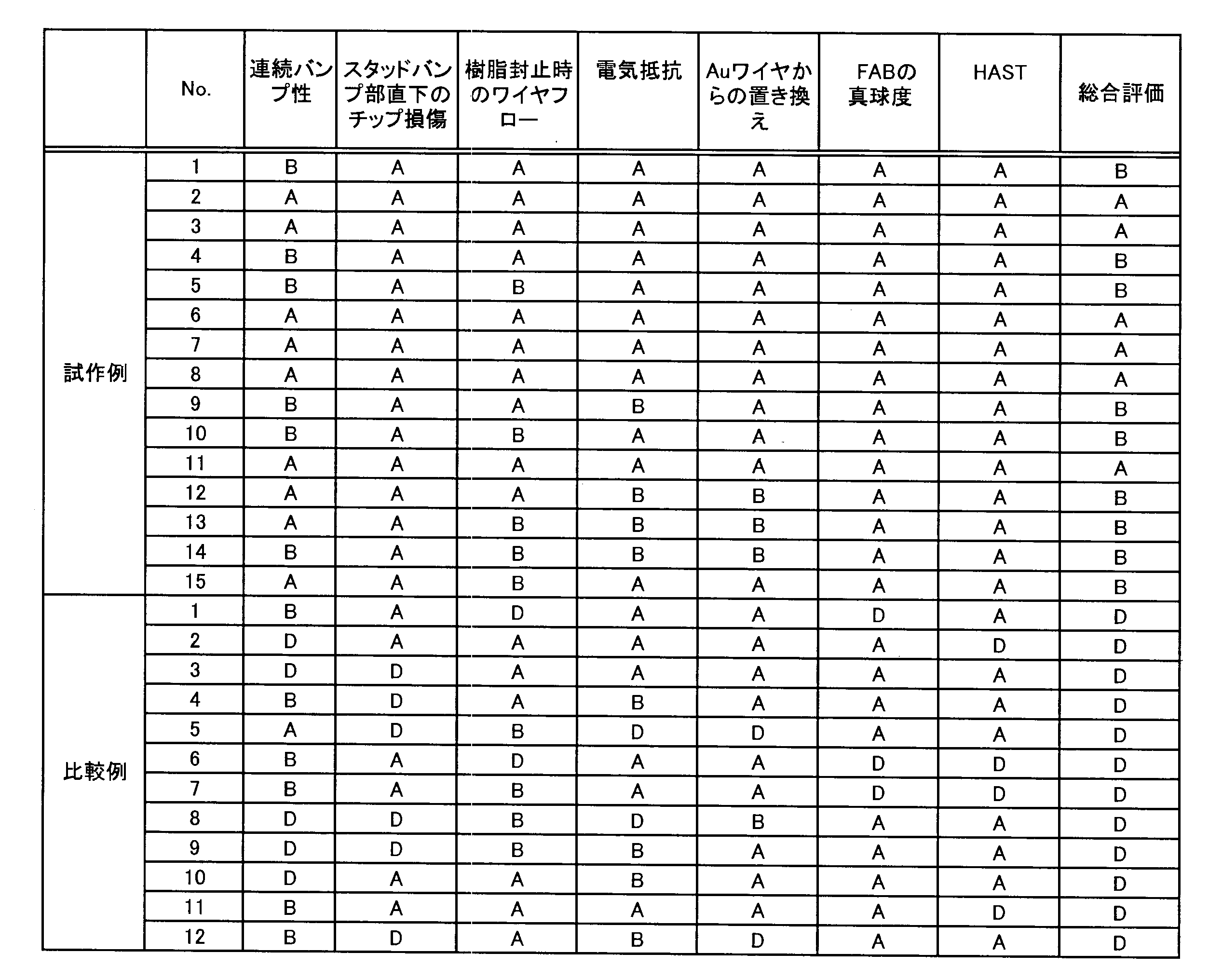
この表1、2において、Auの添加量が0.9質量%未満であったり、添加されなかったりすると、比較例1、6、7から「FABの真球度」が「D」となる。また、同5.0質量%を超えると、比較例5、12から、「Auワイヤからの置き換え」が「D」となる。
また、Pdの添加量が0.1質量%未満であったり、添加されなかったりすると、比較例2、7、11から、「HAST」が「D」となり、5.0質量%を超えると、比較例4から、「スタッドバンプ部真下のチップ損傷」が「D」となる。
さらに、AuとPdの添加量の合計が1.0質量%未満であると、「樹脂封止時のワイヤフロー」が比較例1、6は「D」となり、一方、比較例7は、AuとPdの添加量の合計が1.0質量%未満であるものの、後述のCa、希土類元素から選ばれる1種以上の元素が合計で350質量ppm添加されているため、「樹脂封止時のワイヤフロー」は「B」となる。また、AuとPdの添加量の合計が8質量%を超えると、比較例5、8から、「電気抵抗」が「D」となる。ワイヤWの0.2%耐力(YS)と同引張強さ(TS)との比が80%未満であると、比較例2、3、8~10から「連続バンプ性」が「D」となる。
また、Pdの添加量が0.1質量%未満であったり、添加されなかったりすると、比較例2、7、11から、「HAST」が「D」となり、5.0質量%を超えると、比較例4から、「スタッドバンプ部真下のチップ損傷」が「D」となる。
さらに、AuとPdの添加量の合計が1.0質量%未満であると、「樹脂封止時のワイヤフロー」が比較例1、6は「D」となり、一方、比較例7は、AuとPdの添加量の合計が1.0質量%未満であるものの、後述のCa、希土類元素から選ばれる1種以上の元素が合計で350質量ppm添加されているため、「樹脂封止時のワイヤフロー」は「B」となる。また、AuとPdの添加量の合計が8質量%を超えると、比較例5、8から、「電気抵抗」が「D」となる。ワイヤWの0.2%耐力(YS)と同引張強さ(TS)との比が80%未満であると、比較例2、3、8~10から「連続バンプ性」が「D」となる。
これに対し、この発明に係るAuの添加量を0.9質量%以上5.0質量%以下、Pdの添加量を0.1質量%以上5.0質量%以下、かつAuとPdの添加量の合計を1.0質量%以上8質量%以下とし、そのワイヤWの0.2%耐力と同引張強さとの比が80%以上である試作例1~15にあっては、「連続バンプ性」、「スタッドバンプ部真下のチップ損傷」、「樹脂封止時のワイヤフロー」、「Auワイヤからの置き換え」、「FABの真球度」、「HAST」及び「総合評価」において、「A」又は「B」の何れかであって、実用上、支障なく使用できることが理解できる。
Ca、希土類元素から選ばれる1種以上の元素が合計で20質量ppm未満であると、比較例1、6から、「樹脂封止時のワイヤフロー」が「D」となり、一方、試作例5、13、比較例5は、Ca、希土類元素から選ばれる1種以上の元素が合計で20質量ppm未満であるが、「樹脂封止時のワイヤフロー」性を向上させるAuとPdの添加量の合計が1.0質量%以上であったり、Cu、Niから選ばれる1種以上の元素が合計で1000質量ppm以上であったりすることから、「樹脂封止時のワイヤフロー」が「B」となる。また、Ca、希土類元素から選ばれる1種以上の元素が合計で500質量ppmを超えると、比較例4、8、9から、「スタッドバンプ部真下のチップ損傷」が「D」となる。
また、Cu、Niから選ばれる1種以上の元素が合計で1000質量ppm未満であると、比較例1、6から、「樹脂封止時のワイヤフロー」が「D」となり、一方、試作例10、13~15、比較例7~9はCu、Niから選ばれる1種以上の元素が合計で1000質量ppm未満であるが、「樹脂封止時のワイヤフロー」性を向上させるAuとPdの添加量の合計が1.0質量%以上であったり、Ca、希土類元素から選ばれる1種以上の元素が合計で20質量ppmであったりすることから、「樹脂封止時のワイヤフロー」が「B」となる。また、Cu、Niから選ばれる1種以上の元素が合計で10000質量ppmを超えると、比較例3から「スタッドバンプ部真下のチップ損傷」が「D」となる。
また、ワイヤWの0.2%耐力と同引張強さとの比が80%以上であると、試作例1~15、比較例1、4~7、11、12から、連続バンプ性において「A」又は「B」となるが、90%以上であると、試作例2、3、6~8、11~13、15、比較例5から、連続バンプ性において「A」となり、より優れていることが理解できる。
さらに、Auの添加量を0.9質量%以上2.6質量%以下、Pdの添加量を0.1質量%以上1.5質量%以下、かつAuとPdの添加量の合計を1.0質量%以上3.0質量%以下含むものであると、試作例1~3、6~8から「スタッドバンプ部真下のチップ損傷」、「電気抵抗」、「Auワイヤからの置き換え」、「FABの真球度」、「HAST」において「A」となり、優れていることが理解できる。
ワイヤWの固有抵抗が5.0μΩ・cmを超えると、比較例5、8から、「電気抵抗」が「D」となる。一方、同固有抵抗が3.0μΩ・cm以下に抑えられると、試作例1~8、10、11、15、比較例1~3、6、7、11から「電気抵抗」が「A」となる。
さらに、Auの添加量を0.9質量%以上2.6質量%以下、Pdの添加量を0.1質量%以上1.5質量%以下、かつAuとPdの添加量の合計を1.0質量%以上3.0質量%以下含むものであると、試作例1~3、6~8から「スタッドバンプ部真下のチップ損傷」、「電気抵抗」、「Auワイヤからの置き換え」、「FABの真球度」、「HAST」において「A」となり、優れていることが理解できる。
ワイヤWの固有抵抗が5.0μΩ・cmを超えると、比較例5、8から、「電気抵抗」が「D」となる。一方、同固有抵抗が3.0μΩ・cm以下に抑えられると、試作例1~8、10、11、15、比較例1~3、6、7、11から「電気抵抗」が「A」となる。
以上から、試作例2、3、6~8、11は、ワイヤWの0.2%耐力と同引張強さとの比が90%以上、Auの添加量:0.9質量%以上2.6質量%以下、Pdの添加量:0.1質量%以上1.5質量%以下、かつAuとPdの添加量の合計:1.0質量%以上3.0質量%以下、Ca、希土類元素から選ばれる1種以上の元素を合計で20質量ppm以上500質量ppmを以下、固有抵抗が3.0μΩ・cm以下、Cu、Niから選ばれる1種以上の元素を合計で1000質量ppm以上、10000質量ppm以下であって、総合評価において「A」となっており、最も優れていることが理解できる。
3、13 回路配線基板(ケース電極)
5 半導体素子
15 LED
W ボンディング用ワイヤ
a 半導体素子(LED)の電極
b 溶融ボール
b’ 圧着ボール(スタッドバンプ)
c 回路配線基板の導体配線(リード端子)
5 半導体素子
15 LED
W ボンディング用ワイヤ
a 半導体素子(LED)の電極
b 溶融ボール
b’ 圧着ボール(スタッドバンプ)
c 回路配線基板の導体配線(リード端子)
Claims (7)
- 半導体素子(5、15)の電極(a)と回路配線基板(3、13)の導体配線(c)とをボールボンディング法およびスタッドバンプ法の組合せによって接続するためのボンディング用ワイヤ(W)であって、
Auの添加量を0.9質量%以上5.0質量%以下、Pdの添加量を0.1質量%以上5.0質量%以下、かつAuとPdの添加量の合計を1.0質量%以上8.0質量%以下とし、残部がAgおよび不可避不純物であり、
上記スタッドバンプ法における溶融ボール(b)の作成時、結晶粒の差を生じさせてワイヤ(W)の切断を容易にするために、そのワイヤ(W)の0.2%耐力と同引張強さとの比が80%以上であることを特徴とするボンディング用ワイヤ。 - 上記ワイヤ(W)の組成に、さらにCa、Y、Sm、La、Ceから選ばれる1種以上の元素を合計で20質量ppm以上、500質量ppm以下含むことを特徴とする請求項1に記載のボンディング用ワイヤ。
- 上記ワイヤ(W)の組成に、さらにCu、Niから選ばれる1種以上の元素を合計で1000質量ppm以上、10000質量ppm以下含むことを特徴とする請求項1又は2に記載のボンディング用ワイヤ。
- 上記ワイヤ(W)のAuの添加量を0.9質量%以上2.6質量%以下、Pdの添加量を0.1質量%以上1.5質量%以下、かつAuとPdの添加量の合計を1.0質量%以上3.0質量%以下含むことを特徴とする請求項2又は3に記載のボンディング用ワイヤ。
- 上記ワイヤ(W)の0.2%耐力と同引張強さとの比が90%以上であることを特徴とする請求項1~4の何れか一つに記載のボンディング用ワイヤ。
- 上記ワイヤ(W)の固有抵抗が5.0μΩ・cm以下であることを特徴とする請求項1~3の何れか一つに記載のボンディング用ワイヤ。
- 上記ワイヤ(W)の固有抵抗が3.0μΩ・cm以下であることを特徴とする請求項4又は5に記載のボンディング用ワイヤ。
Priority Applications (2)
| Application Number | Priority Date | Filing Date | Title |
|---|---|---|---|
| CN201480001393.6A CN104380446B (zh) | 2013-03-14 | 2014-03-05 | 焊接用线 |
| KR1020157004000A KR101536554B1 (ko) | 2013-03-14 | 2014-03-05 | 본딩용 와이어 |
Applications Claiming Priority (2)
| Application Number | Priority Date | Filing Date | Title |
|---|---|---|---|
| JP2013-051577 | 2013-03-14 | ||
| JP2013051577A JP5529992B1 (ja) | 2013-03-14 | 2013-03-14 | ボンディング用ワイヤ |
Publications (1)
| Publication Number | Publication Date |
|---|---|
| WO2014141975A1 true WO2014141975A1 (ja) | 2014-09-18 |
Family
ID=51175814
Family Applications (1)
| Application Number | Title | Priority Date | Filing Date |
|---|---|---|---|
| PCT/JP2014/055669 Ceased WO2014141975A1 (ja) | 2013-03-14 | 2014-03-05 | ボンディング用ワイヤ |
Country Status (5)
| Country | Link |
|---|---|
| JP (1) | JP5529992B1 (ja) |
| KR (1) | KR101536554B1 (ja) |
| CN (1) | CN104380446B (ja) |
| TW (1) | TWI490996B (ja) |
| WO (1) | WO2014141975A1 (ja) |
Cited By (2)
| Publication number | Priority date | Publication date | Assignee | Title |
|---|---|---|---|---|
| US10137534B2 (en) | 2015-06-15 | 2018-11-27 | Nippon Micrometal Corporation | Bonding wire for semiconductor device |
| US10468370B2 (en) | 2015-07-23 | 2019-11-05 | Nippon Micrometal Corporation | Bonding wire for semiconductor device |
Families Citing this family (9)
| Publication number | Priority date | Publication date | Assignee | Title |
|---|---|---|---|---|
| SG10201508103QA (en) * | 2015-09-29 | 2017-04-27 | Heraeus Materials Singapore Pte Ltd | Alloyed silver wire |
| MY179434A (en) * | 2016-03-11 | 2020-11-06 | Tatsuta Electric Wire & Cable Co Ltd | Bonding wire |
| TWI609977B (zh) * | 2016-10-17 | 2018-01-01 | 光大應用材料科技股份有限公司 | 銀合金線材 |
| WO2021065036A1 (ja) * | 2019-10-01 | 2021-04-08 | 田中電子工業株式会社 | ワイヤ接合構造とそれに用いられるボンディングワイヤ及び半導体装置 |
| CN111029267B (zh) * | 2019-11-22 | 2021-12-24 | 中国电子科技集团公司第十三研究所 | 一种倒装互连结构及其制备方法 |
| US11636809B2 (en) | 2019-11-29 | 2023-04-25 | Chengdu Boe Optoelectronics Technology Co., Ltd. | Display substrate and display device |
| GB2604433B (en) * | 2020-12-23 | 2023-05-03 | Skyworks Solutions Inc | Apparatus and methods for tool mark free stitch bonding |
| TW202433501A (zh) | 2023-01-31 | 2024-08-16 | 日商拓自達電線股份有限公司 | 接合線 |
| CN117712071A (zh) * | 2023-12-07 | 2024-03-15 | 郑州机械研究所有限公司 | 一种键合线及其制备方法和led器件 |
Citations (6)
| Publication number | Priority date | Publication date | Assignee | Title |
|---|---|---|---|---|
| JP2009033127A (ja) * | 2007-06-28 | 2009-02-12 | Nippon Steel Materials Co Ltd | 半導体実装用ボンディングワイヤ |
| JP2012049198A (ja) * | 2010-08-24 | 2012-03-08 | Sumitomo Metal Mining Co Ltd | 銀ボンディングワイヤ |
| JP2012099577A (ja) * | 2010-10-29 | 2012-05-24 | Sumitomo Metal Mining Co Ltd | ボンディングワイヤ |
| JP2012169374A (ja) * | 2011-02-10 | 2012-09-06 | Tanaka Electronics Ind Co Ltd | Ag−Au−Pd三元合金系ボンディングワイヤ |
| JP2013021280A (ja) * | 2011-07-11 | 2013-01-31 | Profound Material Technology Co Ltd | 複合銀ワイヤ |
| JP2013048169A (ja) * | 2011-08-29 | 2013-03-07 | Tatsuta Electric Wire & Cable Co Ltd | ボールボンディング用ワイヤ |
Family Cites Families (1)
| Publication number | Priority date | Publication date | Assignee | Title |
|---|---|---|---|---|
| JP5064577B2 (ja) * | 2011-01-20 | 2012-10-31 | タツタ電線株式会社 | ボールボンディング用ワイヤ |
-
2013
- 2013-03-14 JP JP2013051577A patent/JP5529992B1/ja active Active
-
2014
- 2014-03-05 CN CN201480001393.6A patent/CN104380446B/zh active Active
- 2014-03-05 KR KR1020157004000A patent/KR101536554B1/ko active Active
- 2014-03-05 WO PCT/JP2014/055669 patent/WO2014141975A1/ja not_active Ceased
- 2014-03-11 TW TW103108465A patent/TWI490996B/zh active
Patent Citations (6)
| Publication number | Priority date | Publication date | Assignee | Title |
|---|---|---|---|---|
| JP2009033127A (ja) * | 2007-06-28 | 2009-02-12 | Nippon Steel Materials Co Ltd | 半導体実装用ボンディングワイヤ |
| JP2012049198A (ja) * | 2010-08-24 | 2012-03-08 | Sumitomo Metal Mining Co Ltd | 銀ボンディングワイヤ |
| JP2012099577A (ja) * | 2010-10-29 | 2012-05-24 | Sumitomo Metal Mining Co Ltd | ボンディングワイヤ |
| JP2012169374A (ja) * | 2011-02-10 | 2012-09-06 | Tanaka Electronics Ind Co Ltd | Ag−Au−Pd三元合金系ボンディングワイヤ |
| JP2013021280A (ja) * | 2011-07-11 | 2013-01-31 | Profound Material Technology Co Ltd | 複合銀ワイヤ |
| JP2013048169A (ja) * | 2011-08-29 | 2013-03-07 | Tatsuta Electric Wire & Cable Co Ltd | ボールボンディング用ワイヤ |
Cited By (5)
| Publication number | Priority date | Publication date | Assignee | Title |
|---|---|---|---|---|
| US10137534B2 (en) | 2015-06-15 | 2018-11-27 | Nippon Micrometal Corporation | Bonding wire for semiconductor device |
| US10414002B2 (en) | 2015-06-15 | 2019-09-17 | Nippon Micrometal Corporation | Bonding wire for semiconductor device |
| US10610976B2 (en) | 2015-06-15 | 2020-04-07 | Nippon Micrometal Corporation | Bonding wire for semiconductor device |
| US10737356B2 (en) | 2015-06-15 | 2020-08-11 | Nippon Micrometal Corporation | Bonding wire for semiconductor device |
| US10468370B2 (en) | 2015-07-23 | 2019-11-05 | Nippon Micrometal Corporation | Bonding wire for semiconductor device |
Also Published As
| Publication number | Publication date |
|---|---|
| CN104380446B (zh) | 2016-03-16 |
| TWI490996B (zh) | 2015-07-01 |
| CN104380446A (zh) | 2015-02-25 |
| KR20150032900A (ko) | 2015-03-30 |
| KR101536554B1 (ko) | 2015-07-13 |
| JP5529992B1 (ja) | 2014-06-25 |
| TW201448152A (zh) | 2014-12-16 |
| JP2014179412A (ja) | 2014-09-25 |
Similar Documents
| Publication | Publication Date | Title |
|---|---|---|
| JP5529992B1 (ja) | ボンディング用ワイヤ | |
| CN103155130B (zh) | Ag-Au-Pd三元合金接合线 | |
| CN102422404B (zh) | 半导体用接合线 | |
| JP5671512B2 (ja) | ボンディング用ワイヤ | |
| JP2010199528A (ja) | ボンディングワイヤ | |
| WO2013018238A1 (ja) | ボールボンディングワイヤ | |
| WO2012043727A1 (ja) | 複層銅ボンディングワイヤの接合構造 | |
| JP5064577B2 (ja) | ボールボンディング用ワイヤ | |
| JP2010245390A (ja) | ボンディングワイヤ | |
| CN115398607A (zh) | 金被覆接合丝线及其制造方法、半导体丝线接合结构、以及半导体装置 | |
| CN103842529B (zh) | 金(Au)合金键合线 | |
| JP6103806B2 (ja) | ボールボンディング用ワイヤ | |
| JP6869919B2 (ja) | ボールボンディング用貴金属被覆銀ワイヤおよびその製造方法、ならびにボールボンディング用貴金属被覆銀ワイヤを使用した半導体装置およびその製造方法 | |
| JP5996853B2 (ja) | ボールボンディング用ワイヤ | |
| JP6343197B2 (ja) | ボンディング用ワイヤ | |
| KR20040073667A (ko) | 반도체 소자용 본딩 와이어 | |
| JP4726206B2 (ja) | 高い初期接合性、高い接合信頼性、圧着ボールの高い真円性、高い直進性、高い耐樹脂流れ性および低い比抵抗を有するボンディングワイヤ用金合金線 | |
| JP2013042105A (ja) | ボンディングワイヤ | |
| JP2011155129A (ja) | 高温半導体装置用金合金ボンディングワイヤ | |
| JP5339101B2 (ja) | バンプ用ワイヤ | |
| JP5403436B2 (ja) | ボールボンディング用ワイヤ | |
| JP2008038201A (ja) | 高い初期接合性、高い接合信頼性、圧着ボールの高い真円性、高いループ制御性および低い比抵抗を有するボンディングワイヤ用金合金線 |
Legal Events
| Date | Code | Title | Description |
|---|---|---|---|
| 121 | Ep: the epo has been informed by wipo that ep was designated in this application |
Ref document number: 14764987 Country of ref document: EP Kind code of ref document: A1 |
|
| ENP | Entry into the national phase |
Ref document number: 20157004000 Country of ref document: KR Kind code of ref document: A |
|
| NENP | Non-entry into the national phase |
Ref country code: DE |
|
| 122 | Ep: pct application non-entry in european phase |
Ref document number: 14764987 Country of ref document: EP Kind code of ref document: A1 |