WO2014123193A1 - 凹凸基板及び発光ダイオードの製造方法、並びに凹凸基板、発光ダイオード及び有機薄膜太陽電池 - Google Patents
凹凸基板及び発光ダイオードの製造方法、並びに凹凸基板、発光ダイオード及び有機薄膜太陽電池 Download PDFInfo
- Publication number
- WO2014123193A1 WO2014123193A1 PCT/JP2014/052781 JP2014052781W WO2014123193A1 WO 2014123193 A1 WO2014123193 A1 WO 2014123193A1 JP 2014052781 W JP2014052781 W JP 2014052781W WO 2014123193 A1 WO2014123193 A1 WO 2014123193A1
- Authority
- WO
- WIPO (PCT)
- Prior art keywords
- concavo
- convex
- particles
- substrate
- layer
- Prior art date
Links
- 239000000758 substrate Substances 0.000 title claims abstract description 149
- 238000000034 method Methods 0.000 title claims abstract description 136
- 238000004519 manufacturing process Methods 0.000 title claims abstract description 31
- 239000010409 thin film Substances 0.000 title claims description 12
- 239000002245 particle Substances 0.000 claims abstract description 300
- 238000005530 etching Methods 0.000 claims abstract description 67
- 239000010410 layer Substances 0.000 claims description 209
- 239000010408 film Substances 0.000 claims description 85
- 230000008569 process Effects 0.000 claims description 56
- XLYOFNOQVPJJNP-UHFFFAOYSA-N water Substances O XLYOFNOQVPJJNP-UHFFFAOYSA-N 0.000 claims description 49
- 239000004065 semiconductor Substances 0.000 claims description 43
- 239000007788 liquid Substances 0.000 claims description 20
- 239000002356 single layer Substances 0.000 claims description 20
- 238000012546 transfer Methods 0.000 claims description 20
- 239000002346 layers by function Substances 0.000 claims description 18
- 239000006185 dispersion Substances 0.000 claims description 13
- 239000002904 solvent Substances 0.000 claims description 13
- 230000007704 transition Effects 0.000 claims description 9
- 238000005401 electroluminescence Methods 0.000 claims description 8
- 238000010030 laminating Methods 0.000 claims description 7
- 230000005484 gravity Effects 0.000 claims description 5
- 238000003475 lamination Methods 0.000 claims description 5
- 239000011295 pitch Substances 0.000 description 45
- 239000000463 material Substances 0.000 description 37
- 230000007547 defect Effects 0.000 description 27
- 238000000605 extraction Methods 0.000 description 26
- 238000001312 dry etching Methods 0.000 description 17
- 238000002347 injection Methods 0.000 description 16
- 239000007924 injection Substances 0.000 description 16
- 239000011230 binding agent Substances 0.000 description 15
- 239000010954 inorganic particle Substances 0.000 description 15
- 229910052751 metal Inorganic materials 0.000 description 15
- 239000002184 metal Substances 0.000 description 15
- 150000004767 nitrides Chemical class 0.000 description 14
- VYPSYNLAJGMNEJ-UHFFFAOYSA-N Silicium dioxide Chemical compound O=[Si]=O VYPSYNLAJGMNEJ-UHFFFAOYSA-N 0.000 description 13
- 238000000089 atomic force micrograph Methods 0.000 description 13
- 239000007789 gas Substances 0.000 description 9
- 230000005525 hole transport Effects 0.000 description 9
- -1 nitride compound Chemical class 0.000 description 9
- 229910052757 nitrogen Inorganic materials 0.000 description 9
- 229910002601 GaN Inorganic materials 0.000 description 8
- 230000000694 effects Effects 0.000 description 8
- 238000005259 measurement Methods 0.000 description 8
- 238000012856 packing Methods 0.000 description 8
- IJGRMHOSHXDMSA-UHFFFAOYSA-N Atomic nitrogen Chemical compound N#N IJGRMHOSHXDMSA-UHFFFAOYSA-N 0.000 description 7
- 230000009467 reduction Effects 0.000 description 7
- 239000000126 substance Substances 0.000 description 7
- 229910052782 aluminium Inorganic materials 0.000 description 6
- 239000000470 constituent Substances 0.000 description 6
- 229910052594 sapphire Inorganic materials 0.000 description 6
- 239000010980 sapphire Substances 0.000 description 6
- XLOMVQKBTHCTTD-UHFFFAOYSA-N Zinc monoxide Chemical compound [Zn]=O XLOMVQKBTHCTTD-UHFFFAOYSA-N 0.000 description 5
- 150000001875 compounds Chemical class 0.000 description 5
- 238000010438 heat treatment Methods 0.000 description 5
- 230000002209 hydrophobic effect Effects 0.000 description 5
- 230000000737 periodic effect Effects 0.000 description 5
- 229910052710 silicon Inorganic materials 0.000 description 5
- 239000000243 solution Substances 0.000 description 5
- QGZKDVFQNNGYKY-UHFFFAOYSA-N Ammonia Chemical compound N QGZKDVFQNNGYKY-UHFFFAOYSA-N 0.000 description 4
- XKRFYHLGVUSROY-UHFFFAOYSA-N Argon Chemical compound [Ar] XKRFYHLGVUSROY-UHFFFAOYSA-N 0.000 description 4
- OAKJQQAXSVQMHS-UHFFFAOYSA-N Hydrazine Chemical compound NN OAKJQQAXSVQMHS-UHFFFAOYSA-N 0.000 description 4
- OAICVXFJPJFONN-UHFFFAOYSA-N Phosphorus Chemical compound [P] OAICVXFJPJFONN-UHFFFAOYSA-N 0.000 description 4
- XUIMIQQOPSSXEZ-UHFFFAOYSA-N Silicon Chemical compound [Si] XUIMIQQOPSSXEZ-UHFFFAOYSA-N 0.000 description 4
- 230000015572 biosynthetic process Effects 0.000 description 4
- 239000003795 chemical substances by application Substances 0.000 description 4
- 239000013078 crystal Substances 0.000 description 4
- 239000011368 organic material Substances 0.000 description 4
- 238000000206 photolithography Methods 0.000 description 4
- 239000010703 silicon Substances 0.000 description 4
- 239000000377 silicon dioxide Substances 0.000 description 4
- 229910052709 silver Inorganic materials 0.000 description 4
- 238000005245 sintering Methods 0.000 description 4
- 239000002002 slurry Substances 0.000 description 4
- ZWEHNKRNPOVVGH-UHFFFAOYSA-N 2-Butanone Chemical compound CCC(C)=O ZWEHNKRNPOVVGH-UHFFFAOYSA-N 0.000 description 3
- CSCPPACGZOOCGX-UHFFFAOYSA-N Acetone Chemical compound CC(C)=O CSCPPACGZOOCGX-UHFFFAOYSA-N 0.000 description 3
- 235000017166 Bambusa arundinacea Nutrition 0.000 description 3
- 235000017491 Bambusa tulda Nutrition 0.000 description 3
- 241001330002 Bambuseae Species 0.000 description 3
- LFQSCWFLJHTTHZ-UHFFFAOYSA-N Ethanol Chemical compound CCO LFQSCWFLJHTTHZ-UHFFFAOYSA-N 0.000 description 3
- XEKOWRVHYACXOJ-UHFFFAOYSA-N Ethyl acetate Chemical compound CCOC(C)=O XEKOWRVHYACXOJ-UHFFFAOYSA-N 0.000 description 3
- OKKJLVBELUTLKV-UHFFFAOYSA-N Methanol Chemical compound OC OKKJLVBELUTLKV-UHFFFAOYSA-N 0.000 description 3
- 235000015334 Phyllostachys viridis Nutrition 0.000 description 3
- YXFVVABEGXRONW-UHFFFAOYSA-N Toluene Chemical compound CC1=CC=CC=C1 YXFVVABEGXRONW-UHFFFAOYSA-N 0.000 description 3
- 125000000217 alkyl group Chemical group 0.000 description 3
- 239000011425 bamboo Substances 0.000 description 3
- 239000008119 colloidal silica Substances 0.000 description 3
- 239000004020 conductor Substances 0.000 description 3
- 230000002950 deficient Effects 0.000 description 3
- 238000009792 diffusion process Methods 0.000 description 3
- 239000011521 glass Substances 0.000 description 3
- 229910021478 group 5 element Inorganic materials 0.000 description 3
- 230000006872 improvement Effects 0.000 description 3
- 229910010272 inorganic material Inorganic materials 0.000 description 3
- 239000011147 inorganic material Substances 0.000 description 3
- PQXKHYXIUOZZFA-UHFFFAOYSA-M lithium fluoride Chemical compound [Li+].[F-] PQXKHYXIUOZZFA-UHFFFAOYSA-M 0.000 description 3
- 150000002739 metals Chemical class 0.000 description 3
- VLKZOEOYAKHREP-UHFFFAOYSA-N n-Hexane Chemical compound CCCCCC VLKZOEOYAKHREP-UHFFFAOYSA-N 0.000 description 3
- 239000002994 raw material Substances 0.000 description 3
- RHUYHJGZWVXEHW-UHFFFAOYSA-N 1,1-Dimethyhydrazine Chemical compound CN(C)N RHUYHJGZWVXEHW-UHFFFAOYSA-N 0.000 description 2
- 229910002704 AlGaN Inorganic materials 0.000 description 2
- 238000012935 Averaging Methods 0.000 description 2
- OKTJSMMVPCPJKN-UHFFFAOYSA-N Carbon Chemical compound [C] OKTJSMMVPCPJKN-UHFFFAOYSA-N 0.000 description 2
- HEDRZPFGACZZDS-UHFFFAOYSA-N Chloroform Chemical compound ClC(Cl)Cl HEDRZPFGACZZDS-UHFFFAOYSA-N 0.000 description 2
- RYGMFSIKBFXOCR-UHFFFAOYSA-N Copper Chemical compound [Cu] RYGMFSIKBFXOCR-UHFFFAOYSA-N 0.000 description 2
- VEXZGXHMUGYJMC-UHFFFAOYSA-N Hydrochloric acid Chemical compound Cl VEXZGXHMUGYJMC-UHFFFAOYSA-N 0.000 description 2
- 229910021617 Indium monochloride Inorganic materials 0.000 description 2
- KFZMGEQAYNKOFK-UHFFFAOYSA-N Isopropanol Chemical compound CC(C)O KFZMGEQAYNKOFK-UHFFFAOYSA-N 0.000 description 2
- 229910003902 SiCl 4 Inorganic materials 0.000 description 2
- GWEVSGVZZGPLCZ-UHFFFAOYSA-N Titan oxide Chemical compound O=[Ti]=O GWEVSGVZZGPLCZ-UHFFFAOYSA-N 0.000 description 2
- MCMNRKCIXSYSNV-UHFFFAOYSA-N Zirconium dioxide Chemical compound O=[Zr]=O MCMNRKCIXSYSNV-UHFFFAOYSA-N 0.000 description 2
- 229910045601 alloy Inorganic materials 0.000 description 2
- 239000000956 alloy Substances 0.000 description 2
- XAGFODPZIPBFFR-UHFFFAOYSA-N aluminium Chemical compound [Al] XAGFODPZIPBFFR-UHFFFAOYSA-N 0.000 description 2
- JNDMLEXHDPKVFC-UHFFFAOYSA-N aluminum;oxygen(2-);yttrium(3+) Chemical compound [O-2].[O-2].[O-2].[Al+3].[Y+3] JNDMLEXHDPKVFC-UHFFFAOYSA-N 0.000 description 2
- 229910021529 ammonia Inorganic materials 0.000 description 2
- 229910052786 argon Inorganic materials 0.000 description 2
- 239000012298 atmosphere Substances 0.000 description 2
- 230000004888 barrier function Effects 0.000 description 2
- 230000008901 benefit Effects 0.000 description 2
- 239000000872 buffer Substances 0.000 description 2
- 229910002091 carbon monoxide Inorganic materials 0.000 description 2
- 230000008859 change Effects 0.000 description 2
- 238000012790 confirmation Methods 0.000 description 2
- 229910052802 copper Inorganic materials 0.000 description 2
- 239000010949 copper Substances 0.000 description 2
- PMHQVHHXPFUNSP-UHFFFAOYSA-M copper(1+);methylsulfanylmethane;bromide Chemical compound Br[Cu].CSC PMHQVHHXPFUNSP-UHFFFAOYSA-M 0.000 description 2
- 230000007423 decrease Effects 0.000 description 2
- 239000002612 dispersion medium Substances 0.000 description 2
- 229910052737 gold Inorganic materials 0.000 description 2
- 125000005843 halogen group Chemical group 0.000 description 2
- 229910052734 helium Inorganic materials 0.000 description 2
- 239000001307 helium Substances 0.000 description 2
- SWQJXJOGLNCZEY-UHFFFAOYSA-N helium atom Chemical compound [He] SWQJXJOGLNCZEY-UHFFFAOYSA-N 0.000 description 2
- 238000002248 hydride vapour-phase epitaxy Methods 0.000 description 2
- 239000001257 hydrogen Substances 0.000 description 2
- 229910052739 hydrogen Inorganic materials 0.000 description 2
- APHGZSBLRQFRCA-UHFFFAOYSA-M indium(1+);chloride Chemical compound [In]Cl APHGZSBLRQFRCA-UHFFFAOYSA-M 0.000 description 2
- AMGQUBHHOARCQH-UHFFFAOYSA-N indium;oxotin Chemical compound [In].[Sn]=O AMGQUBHHOARCQH-UHFFFAOYSA-N 0.000 description 2
- 229910052741 iridium Inorganic materials 0.000 description 2
- GKOZUEZYRPOHIO-UHFFFAOYSA-N iridium atom Chemical compound [Ir] GKOZUEZYRPOHIO-UHFFFAOYSA-N 0.000 description 2
- NDBCGHNTWCYIIU-UHFFFAOYSA-N iridium(3+);1-phenylisoquinoline Chemical compound [Ir+3].[C-]1=CC=CC=C1C1=NC=CC2=CC=CC=C12.[C-]1=CC=CC=C1C1=NC=CC2=CC=CC=C12.[C-]1=CC=CC=C1C1=NC=CC2=CC=CC=C12 NDBCGHNTWCYIIU-UHFFFAOYSA-N 0.000 description 2
- 239000011777 magnesium Substances 0.000 description 2
- 239000002609 medium Substances 0.000 description 2
- 238000002488 metal-organic chemical vapour deposition Methods 0.000 description 2
- 239000000203 mixture Substances 0.000 description 2
- 238000001451 molecular beam epitaxy Methods 0.000 description 2
- 229910052759 nickel Inorganic materials 0.000 description 2
- 230000003647 oxidation Effects 0.000 description 2
- 238000007254 oxidation reaction Methods 0.000 description 2
- KYKLWYKWCAYAJY-UHFFFAOYSA-N oxotin;zinc Chemical compound [Zn].[Sn]=O KYKLWYKWCAYAJY-UHFFFAOYSA-N 0.000 description 2
- 239000011164 primary particle Substances 0.000 description 2
- 230000005855 radiation Effects 0.000 description 2
- 239000011347 resin Substances 0.000 description 2
- 229920005989 resin Polymers 0.000 description 2
- 150000003346 selenoethers Chemical class 0.000 description 2
- 238000001228 spectrum Methods 0.000 description 2
- 239000004094 surface-active agent Substances 0.000 description 2
- 229910052719 titanium Inorganic materials 0.000 description 2
- 238000002834 transmittance Methods 0.000 description 2
- GETQZCLCWQTVFV-UHFFFAOYSA-N trimethylamine Chemical compound CN(C)C GETQZCLCWQTVFV-UHFFFAOYSA-N 0.000 description 2
- 238000001771 vacuum deposition Methods 0.000 description 2
- 229910019901 yttrium aluminum garnet Inorganic materials 0.000 description 2
- YVTHLONGBIQYBO-UHFFFAOYSA-N zinc indium(3+) oxygen(2-) Chemical compound [O--].[Zn++].[In+3] YVTHLONGBIQYBO-UHFFFAOYSA-N 0.000 description 2
- 239000011787 zinc oxide Substances 0.000 description 2
- PFNQVRZLDWYSCW-UHFFFAOYSA-N (fluoren-9-ylideneamino) n-naphthalen-1-ylcarbamate Chemical compound C12=CC=CC=C2C2=CC=CC=C2C1=NOC(=O)NC1=CC=CC2=CC=CC=C12 PFNQVRZLDWYSCW-UHFFFAOYSA-N 0.000 description 1
- DIIIISSCIXVANO-UHFFFAOYSA-N 1,2-Dimethylhydrazine Chemical compound CNNC DIIIISSCIXVANO-UHFFFAOYSA-N 0.000 description 1
- MXVLMYZRJAHEIS-UHFFFAOYSA-N 1-(2-phenylphenyl)naphthalene Chemical group C1=CC=CC=C1C1=CC=CC=C1C1=CC=CC2=CC=CC=C12 MXVLMYZRJAHEIS-UHFFFAOYSA-N 0.000 description 1
- MUNFOTHAFHGRIM-UHFFFAOYSA-N 2,5-dinaphthalen-1-yl-1,3,4-oxadiazole Chemical compound C1=CC=C2C(C3=NN=C(O3)C=3C4=CC=CC=C4C=CC=3)=CC=CC2=C1 MUNFOTHAFHGRIM-UHFFFAOYSA-N 0.000 description 1
- UOCMXZLNHQBBOS-UHFFFAOYSA-N 2-(1,3-benzoxazol-2-yl)phenol zinc Chemical compound [Zn].Oc1ccccc1-c1nc2ccccc2o1.Oc1ccccc1-c1nc2ccccc2o1 UOCMXZLNHQBBOS-UHFFFAOYSA-N 0.000 description 1
- WUPHOULIZUERAE-UHFFFAOYSA-N 3-(oxolan-2-yl)propanoic acid Chemical compound OC(=O)CCC1CCCO1 WUPHOULIZUERAE-UHFFFAOYSA-N 0.000 description 1
- OGGKVJMNFFSDEV-UHFFFAOYSA-N 3-methyl-n-[4-[4-(n-(3-methylphenyl)anilino)phenyl]phenyl]-n-phenylaniline Chemical compound CC1=CC=CC(N(C=2C=CC=CC=2)C=2C=CC(=CC=2)C=2C=CC(=CC=2)N(C=2C=CC=CC=2)C=2C=C(C)C=CC=2)=C1 OGGKVJMNFFSDEV-UHFFFAOYSA-N 0.000 description 1
- YPSXFMHXRZAGTG-UHFFFAOYSA-N 4-methoxy-2-[2-(5-methoxy-2-nitrosophenyl)ethyl]-1-nitrosobenzene Chemical compound COC1=CC=C(N=O)C(CCC=2C(=CC=C(OC)C=2)N=O)=C1 YPSXFMHXRZAGTG-UHFFFAOYSA-N 0.000 description 1
- 229910052580 B4C Inorganic materials 0.000 description 1
- 229910052582 BN Inorganic materials 0.000 description 1
- PZNSFCLAULLKQX-UHFFFAOYSA-N Boron nitride Chemical compound N#B PZNSFCLAULLKQX-UHFFFAOYSA-N 0.000 description 1
- DKPFZGUDAPQIHT-UHFFFAOYSA-N Butyl acetate Natural products CCCCOC(C)=O DKPFZGUDAPQIHT-UHFFFAOYSA-N 0.000 description 1
- XMWRBQBLMFGWIX-UHFFFAOYSA-N C60 fullerene Chemical class C12=C3C(C4=C56)=C7C8=C5C5=C9C%10=C6C6=C4C1=C1C4=C6C6=C%10C%10=C9C9=C%11C5=C8C5=C8C7=C3C3=C7C2=C1C1=C2C4=C6C4=C%10C6=C9C9=C%11C5=C5C8=C3C3=C7C1=C1C2=C4C6=C2C9=C5C3=C12 XMWRBQBLMFGWIX-UHFFFAOYSA-N 0.000 description 1
- 229910052684 Cerium Inorganic materials 0.000 description 1
- VEXZGXHMUGYJMC-UHFFFAOYSA-M Chloride anion Chemical compound [Cl-] VEXZGXHMUGYJMC-UHFFFAOYSA-M 0.000 description 1
- XDTMQSROBMDMFD-UHFFFAOYSA-N Cyclohexane Chemical compound C1CCCCC1 XDTMQSROBMDMFD-UHFFFAOYSA-N 0.000 description 1
- PIICEJLVQHRZGT-UHFFFAOYSA-N Ethylenediamine Chemical compound NCCN PIICEJLVQHRZGT-UHFFFAOYSA-N 0.000 description 1
- 229910052693 Europium Inorganic materials 0.000 description 1
- 229920002430 Fibre-reinforced plastic Polymers 0.000 description 1
- JMASRVWKEDWRBT-UHFFFAOYSA-N Gallium nitride Chemical compound [Ga]#N JMASRVWKEDWRBT-UHFFFAOYSA-N 0.000 description 1
- UFHFLCQGNIYNRP-UHFFFAOYSA-N Hydrogen Chemical compound [H][H] UFHFLCQGNIYNRP-UHFFFAOYSA-N 0.000 description 1
- 229910000861 Mg alloy Inorganic materials 0.000 description 1
- 229910020068 MgAl Inorganic materials 0.000 description 1
- 239000004793 Polystyrene Substances 0.000 description 1
- 229910052581 Si3N4 Inorganic materials 0.000 description 1
- UCKMPCXJQFINFW-UHFFFAOYSA-N Sulphide Chemical compound [S-2] UCKMPCXJQFINFW-UHFFFAOYSA-N 0.000 description 1
- 239000007983 Tris buffer Substances 0.000 description 1
- 239000005083 Zinc sulfide Substances 0.000 description 1
- 238000010521 absorption reaction Methods 0.000 description 1
- 239000012190 activator Substances 0.000 description 1
- 229910000086 alane Inorganic materials 0.000 description 1
- AZDRQVAHHNSJOQ-UHFFFAOYSA-N alumane Chemical compound [AlH3] AZDRQVAHHNSJOQ-UHFFFAOYSA-N 0.000 description 1
- PNEYBMLMFCGWSK-UHFFFAOYSA-N aluminium oxide Inorganic materials [O-2].[O-2].[O-2].[Al+3].[Al+3] PNEYBMLMFCGWSK-UHFFFAOYSA-N 0.000 description 1
- QVGXLLKOCUKJST-UHFFFAOYSA-N atomic oxygen Chemical compound [O] QVGXLLKOCUKJST-UHFFFAOYSA-N 0.000 description 1
- NWAIGJYBQQYSPW-UHFFFAOYSA-N azanylidyneindigane Chemical compound [In]#N NWAIGJYBQQYSPW-UHFFFAOYSA-N 0.000 description 1
- INAHAJYZKVIDIZ-UHFFFAOYSA-N boron carbide Chemical compound B12B3B4C32B41 INAHAJYZKVIDIZ-UHFFFAOYSA-N 0.000 description 1
- 229910052795 boron group element Inorganic materials 0.000 description 1
- 229910052794 bromium Inorganic materials 0.000 description 1
- 229910052980 cadmium sulfide Inorganic materials 0.000 description 1
- UHYPYGJEEGLRJD-UHFFFAOYSA-N cadmium(2+);selenium(2-) Chemical compound [Se-2].[Cd+2] UHYPYGJEEGLRJD-UHFFFAOYSA-N 0.000 description 1
- 229910052791 calcium Inorganic materials 0.000 description 1
- 239000011575 calcium Substances 0.000 description 1
- JGIATAMCQXIDNZ-UHFFFAOYSA-N calcium sulfide Chemical compound [Ca]=S JGIATAMCQXIDNZ-UHFFFAOYSA-N 0.000 description 1
- 229910052799 carbon Inorganic materials 0.000 description 1
- 125000004432 carbon atom Chemical group C* 0.000 description 1
- 239000012159 carrier gas Substances 0.000 description 1
- 239000001913 cellulose Substances 0.000 description 1
- 229920002678 cellulose Polymers 0.000 description 1
- CETPSERCERDGAM-UHFFFAOYSA-N ceric oxide Chemical compound O=[Ce]=O CETPSERCERDGAM-UHFFFAOYSA-N 0.000 description 1
- ZMIGMASIKSOYAM-UHFFFAOYSA-N cerium Chemical compound [Ce][Ce][Ce][Ce][Ce][Ce][Ce][Ce][Ce][Ce][Ce][Ce][Ce][Ce][Ce][Ce][Ce][Ce][Ce][Ce][Ce][Ce][Ce][Ce][Ce][Ce][Ce][Ce][Ce][Ce][Ce][Ce][Ce][Ce][Ce][Ce][Ce][Ce] ZMIGMASIKSOYAM-UHFFFAOYSA-N 0.000 description 1
- 229910000422 cerium(IV) oxide Inorganic materials 0.000 description 1
- 229910052801 chlorine Inorganic materials 0.000 description 1
- 229910052804 chromium Inorganic materials 0.000 description 1
- 239000011651 chromium Substances 0.000 description 1
- 238000004140 cleaning Methods 0.000 description 1
- 239000011248 coating agent Substances 0.000 description 1
- 238000000576 coating method Methods 0.000 description 1
- 239000003086 colorant Substances 0.000 description 1
- 239000013065 commercial product Substances 0.000 description 1
- 238000011109 contamination Methods 0.000 description 1
- 238000007796 conventional method Methods 0.000 description 1
- 238000005520 cutting process Methods 0.000 description 1
- 150000001925 cycloalkenes Chemical class 0.000 description 1
- 238000000151 deposition Methods 0.000 description 1
- 230000008021 deposition Effects 0.000 description 1
- 238000010586 diagram Methods 0.000 description 1
- 150000004985 diamines Chemical class 0.000 description 1
- 229910003460 diamond Inorganic materials 0.000 description 1
- 239000010432 diamond Substances 0.000 description 1
- 239000000539 dimer Substances 0.000 description 1
- 238000006073 displacement reaction Methods 0.000 description 1
- 238000009826 distribution Methods 0.000 description 1
- 238000001035 drying Methods 0.000 description 1
- 238000002296 dynamic light scattering Methods 0.000 description 1
- 230000005684 electric field Effects 0.000 description 1
- 238000005323 electroforming Methods 0.000 description 1
- 238000000635 electron micrograph Methods 0.000 description 1
- 238000004049 embossing Methods 0.000 description 1
- 230000007613 environmental effect Effects 0.000 description 1
- OGPBJKLSAFTDLK-UHFFFAOYSA-N europium atom Chemical compound [Eu] OGPBJKLSAFTDLK-UHFFFAOYSA-N 0.000 description 1
- 239000000284 extract Substances 0.000 description 1
- 239000000835 fiber Substances 0.000 description 1
- 239000011151 fibre-reinforced plastic Substances 0.000 description 1
- 238000011049 filling Methods 0.000 description 1
- 239000005357 flat glass Substances 0.000 description 1
- 238000007667 floating Methods 0.000 description 1
- 229910052731 fluorine Inorganic materials 0.000 description 1
- 229910003472 fullerene Inorganic materials 0.000 description 1
- 230000004927 fusion Effects 0.000 description 1
- 229910002804 graphite Inorganic materials 0.000 description 1
- 239000010439 graphite Substances 0.000 description 1
- JEGUKCSWCFPDGT-UHFFFAOYSA-N h2o hydrate Chemical compound O.O JEGUKCSWCFPDGT-UHFFFAOYSA-N 0.000 description 1
- RBTKNAXYKSUFRK-UHFFFAOYSA-N heliogen blue Chemical compound [Cu].[N-]1C2=C(C=CC=C3)C3=C1N=C([N-]1)C3=CC=CC=C3C1=NC([N-]1)=C(C=CC=C3)C3=C1N=C([N-]1)C3=CC=CC=C3C1=N2 RBTKNAXYKSUFRK-UHFFFAOYSA-N 0.000 description 1
- FUZZWVXGSFPDMH-UHFFFAOYSA-N hexanoic acid Chemical compound CCCCCC(O)=O FUZZWVXGSFPDMH-UHFFFAOYSA-N 0.000 description 1
- 150000002431 hydrogen Chemical class 0.000 description 1
- 230000005661 hydrophobic surface Effects 0.000 description 1
- 238000005286 illumination Methods 0.000 description 1
- 230000001771 impaired effect Effects 0.000 description 1
- 229910052738 indium Inorganic materials 0.000 description 1
- PSCMQHVBLHHWTO-UHFFFAOYSA-K indium(iii) chloride Chemical group Cl[In](Cl)Cl PSCMQHVBLHHWTO-UHFFFAOYSA-K 0.000 description 1
- 238000001746 injection moulding Methods 0.000 description 1
- 229910052500 inorganic mineral Inorganic materials 0.000 description 1
- 239000012212 insulator Substances 0.000 description 1
- 238000010406 interfacial reaction Methods 0.000 description 1
- 238000010884 ion-beam technique Methods 0.000 description 1
- 230000001678 irradiating effect Effects 0.000 description 1
- 150000002642 lithium compounds Chemical class 0.000 description 1
- 238000001459 lithography Methods 0.000 description 1
- 229910052749 magnesium Inorganic materials 0.000 description 1
- 230000008018 melting Effects 0.000 description 1
- 238000002844 melting Methods 0.000 description 1
- 239000012528 membrane Substances 0.000 description 1
- 150000001247 metal acetylides Chemical class 0.000 description 1
- 229910044991 metal oxide Inorganic materials 0.000 description 1
- 150000004706 metal oxides Chemical class 0.000 description 1
- 239000002923 metal particle Substances 0.000 description 1
- 239000010445 mica Substances 0.000 description 1
- 229910052618 mica group Inorganic materials 0.000 description 1
- 238000001471 micro-filtration Methods 0.000 description 1
- 229910003465 moissanite Inorganic materials 0.000 description 1
- HDZGCSFEDULWCS-UHFFFAOYSA-N monomethylhydrazine Chemical compound CNN HDZGCSFEDULWCS-UHFFFAOYSA-N 0.000 description 1
- ZOQXMEDOTSCWAG-UHFFFAOYSA-N n-phenyl-n-(2-phenylethenyl)aniline Chemical compound C=1C=CC=CC=1N(C=1C=CC=CC=1)C=CC1=CC=CC=C1 ZOQXMEDOTSCWAG-UHFFFAOYSA-N 0.000 description 1
- 239000002121 nanofiber Substances 0.000 description 1
- 239000002105 nanoparticle Substances 0.000 description 1
- QJGQUHMNIGDVPM-UHFFFAOYSA-N nitrogen group Chemical group [N] QJGQUHMNIGDVPM-UHFFFAOYSA-N 0.000 description 1
- 230000003287 optical effect Effects 0.000 description 1
- 229920000620 organic polymer Polymers 0.000 description 1
- 239000003960 organic solvent Substances 0.000 description 1
- 125000002524 organometallic group Chemical group 0.000 description 1
- 150000004866 oxadiazoles Chemical class 0.000 description 1
- 229910052760 oxygen Inorganic materials 0.000 description 1
- 239000001301 oxygen Substances 0.000 description 1
- 229910052763 palladium Inorganic materials 0.000 description 1
- FDPIMTJIUBPUKL-UHFFFAOYSA-N pentan-3-one Chemical compound CCC(=O)CC FDPIMTJIUBPUKL-UHFFFAOYSA-N 0.000 description 1
- 239000000049 pigment Substances 0.000 description 1
- 238000001020 plasma etching Methods 0.000 description 1
- 229910052697 platinum Inorganic materials 0.000 description 1
- 229910052696 pnictogen Inorganic materials 0.000 description 1
- 229920003229 poly(methyl methacrylate) Polymers 0.000 description 1
- 229920006267 polyester film Polymers 0.000 description 1
- 239000004926 polymethyl methacrylate Substances 0.000 description 1
- 229920005553 polystyrene-acrylate Polymers 0.000 description 1
- 238000010248 power generation Methods 0.000 description 1
- 238000012545 processing Methods 0.000 description 1
- 230000001902 propagating effect Effects 0.000 description 1
- 239000010453 quartz Substances 0.000 description 1
- 230000008707 rearrangement Effects 0.000 description 1
- 230000004044 response Effects 0.000 description 1
- 229910052703 rhodium Inorganic materials 0.000 description 1
- 239000011163 secondary particle Substances 0.000 description 1
- 229910010271 silicon carbide Inorganic materials 0.000 description 1
- HQVNEWCFYHHQES-UHFFFAOYSA-N silicon nitride Chemical compound N12[Si]34N5[Si]62N3[Si]51N64 HQVNEWCFYHHQES-UHFFFAOYSA-N 0.000 description 1
- 239000004332 silver Substances 0.000 description 1
- 238000001179 sorption measurement Methods 0.000 description 1
- 238000005507 spraying Methods 0.000 description 1
- 238000004544 sputter deposition Methods 0.000 description 1
- ZEGFMFQPWDMMEP-UHFFFAOYSA-N strontium;sulfide Chemical compound [S-2].[Sr+2] ZEGFMFQPWDMMEP-UHFFFAOYSA-N 0.000 description 1
- 150000004763 sulfides Chemical class 0.000 description 1
- 229910052715 tantalum Inorganic materials 0.000 description 1
- YBRBMKDOPFTVDT-UHFFFAOYSA-N tert-butylamine Chemical compound CC(C)(C)N YBRBMKDOPFTVDT-UHFFFAOYSA-N 0.000 description 1
- XOLBLPGZBRYERU-UHFFFAOYSA-N tin dioxide Chemical compound O=[Sn]=O XOLBLPGZBRYERU-UHFFFAOYSA-N 0.000 description 1
- 229910001887 tin oxide Inorganic materials 0.000 description 1
- 239000010936 titanium Substances 0.000 description 1
- TVIVIEFSHFOWTE-UHFFFAOYSA-K tri(quinolin-8-yloxy)alumane Chemical compound [Al+3].C1=CN=C2C([O-])=CC=CC2=C1.C1=CN=C2C([O-])=CC=CC2=C1.C1=CN=C2C([O-])=CC=CC2=C1 TVIVIEFSHFOWTE-UHFFFAOYSA-K 0.000 description 1
- VOITXYVAKOUIBA-UHFFFAOYSA-N triethylaluminium Chemical compound CC[Al](CC)CC VOITXYVAKOUIBA-UHFFFAOYSA-N 0.000 description 1
- RGGPNXQUMRMPRA-UHFFFAOYSA-N triethylgallium Chemical compound CC[Ga](CC)CC RGGPNXQUMRMPRA-UHFFFAOYSA-N 0.000 description 1
- OTRPZROOJRIMKW-UHFFFAOYSA-N triethylindigane Chemical compound CC[In](CC)CC OTRPZROOJRIMKW-UHFFFAOYSA-N 0.000 description 1
- MCULRUJILOGHCJ-UHFFFAOYSA-N triisobutylaluminium Chemical compound CC(C)C[Al](CC(C)C)CC(C)C MCULRUJILOGHCJ-UHFFFAOYSA-N 0.000 description 1
- JLTRXTDYQLMHGR-UHFFFAOYSA-N trimethylaluminium Chemical compound C[Al](C)C JLTRXTDYQLMHGR-UHFFFAOYSA-N 0.000 description 1
- XCZXGTMEAKBVPV-UHFFFAOYSA-N trimethylgallium Chemical compound C[Ga](C)C XCZXGTMEAKBVPV-UHFFFAOYSA-N 0.000 description 1
- IBEFSUTVZWZJEL-UHFFFAOYSA-N trimethylindium Chemical compound C[In](C)C IBEFSUTVZWZJEL-UHFFFAOYSA-N 0.000 description 1
- ODHXBMXNKOYIBV-UHFFFAOYSA-N triphenylamine Chemical compound C1=CC=CC=C1N(C=1C=CC=CC=1)C1=CC=CC=C1 ODHXBMXNKOYIBV-UHFFFAOYSA-N 0.000 description 1
- 229910052721 tungsten Inorganic materials 0.000 description 1
- 238000000927 vapour-phase epitaxy Methods 0.000 description 1
- 229910052725 zinc Inorganic materials 0.000 description 1
- 239000011701 zinc Substances 0.000 description 1
- 229910052984 zinc sulfide Inorganic materials 0.000 description 1
- DRDVZXDWVBGGMH-UHFFFAOYSA-N zinc;sulfide Chemical compound [S-2].[Zn+2] DRDVZXDWVBGGMH-UHFFFAOYSA-N 0.000 description 1
Images


Classifications
-
- H—ELECTRICITY
- H01—ELECTRIC ELEMENTS
- H01L—SEMICONDUCTOR DEVICES NOT COVERED BY CLASS H10
- H01L33/00—Semiconductor devices with at least one potential-jump barrier or surface barrier specially adapted for light emission; Processes or apparatus specially adapted for the manufacture or treatment thereof or of parts thereof; Details thereof
- H01L33/02—Semiconductor devices with at least one potential-jump barrier or surface barrier specially adapted for light emission; Processes or apparatus specially adapted for the manufacture or treatment thereof or of parts thereof; Details thereof characterised by the semiconductor bodies
- H01L33/20—Semiconductor devices with at least one potential-jump barrier or surface barrier specially adapted for light emission; Processes or apparatus specially adapted for the manufacture or treatment thereof or of parts thereof; Details thereof characterised by the semiconductor bodies with a particular shape, e.g. curved or truncated substrate
- H01L33/22—Roughened surfaces, e.g. at the interface between epitaxial layers
-
- H—ELECTRICITY
- H10—SEMICONDUCTOR DEVICES; ELECTRIC SOLID-STATE DEVICES NOT OTHERWISE PROVIDED FOR
- H10K—ORGANIC ELECTRIC SOLID-STATE DEVICES
- H10K30/00—Organic devices sensitive to infrared radiation, light, electromagnetic radiation of shorter wavelength or corpuscular radiation
- H10K30/80—Constructional details
- H10K30/87—Light-trapping means
-
- H—ELECTRICITY
- H10—SEMICONDUCTOR DEVICES; ELECTRIC SOLID-STATE DEVICES NOT OTHERWISE PROVIDED FOR
- H10K—ORGANIC ELECTRIC SOLID-STATE DEVICES
- H10K50/00—Organic light-emitting devices
- H10K50/80—Constructional details
- H10K50/85—Arrangements for extracting light from the devices
- H10K50/858—Arrangements for extracting light from the devices comprising refractive means, e.g. lenses
-
- H—ELECTRICITY
- H10—SEMICONDUCTOR DEVICES; ELECTRIC SOLID-STATE DEVICES NOT OTHERWISE PROVIDED FOR
- H10K—ORGANIC ELECTRIC SOLID-STATE DEVICES
- H10K77/00—Constructional details of devices covered by this subclass and not covered by groups H10K10/80, H10K30/80, H10K50/80 or H10K59/80
- H10K77/10—Substrates, e.g. flexible substrates
-
- H—ELECTRICITY
- H01—ELECTRIC ELEMENTS
- H01L—SEMICONDUCTOR DEVICES NOT COVERED BY CLASS H10
- H01L2933/00—Details relating to devices covered by the group H01L33/00 but not provided for in its subgroups
- H01L2933/0091—Scattering means in or on the semiconductor body or semiconductor body package
-
- Y—GENERAL TAGGING OF NEW TECHNOLOGICAL DEVELOPMENTS; GENERAL TAGGING OF CROSS-SECTIONAL TECHNOLOGIES SPANNING OVER SEVERAL SECTIONS OF THE IPC; TECHNICAL SUBJECTS COVERED BY FORMER USPC CROSS-REFERENCE ART COLLECTIONS [XRACs] AND DIGESTS
- Y02—TECHNOLOGIES OR APPLICATIONS FOR MITIGATION OR ADAPTATION AGAINST CLIMATE CHANGE
- Y02E—REDUCTION OF GREENHOUSE GAS [GHG] EMISSIONS, RELATED TO ENERGY GENERATION, TRANSMISSION OR DISTRIBUTION
- Y02E10/00—Energy generation through renewable energy sources
- Y02E10/50—Photovoltaic [PV] energy
- Y02E10/549—Organic PV cells
-
- Y—GENERAL TAGGING OF NEW TECHNOLOGICAL DEVELOPMENTS; GENERAL TAGGING OF CROSS-SECTIONAL TECHNOLOGIES SPANNING OVER SEVERAL SECTIONS OF THE IPC; TECHNICAL SUBJECTS COVERED BY FORMER USPC CROSS-REFERENCE ART COLLECTIONS [XRACs] AND DIGESTS
- Y02—TECHNOLOGIES OR APPLICATIONS FOR MITIGATION OR ADAPTATION AGAINST CLIMATE CHANGE
- Y02P—CLIMATE CHANGE MITIGATION TECHNOLOGIES IN THE PRODUCTION OR PROCESSING OF GOODS
- Y02P70/00—Climate change mitigation technologies in the production process for final industrial or consumer products
- Y02P70/50—Manufacturing or production processes characterised by the final manufactured product
Definitions
- the present invention relates to a concavo-convex substrate suitable for manufacturing photoelectric devices such as organic or inorganic light-emitting diodes, photodiodes, and photovoltaic cells, a method for manufacturing an organic or inorganic light-emitting diode, and a concavo-convex substrate, organic or inorganic light-emitting diodes and organic
- the present invention relates to a thin film solar cell.
- An organic light emitting diode is a light emitting element using organic electroluminescence (hereinafter referred to as organic EL), and generally an anode and a cathode are provided on both sides of an organic EL layer including a light emitting layer containing an organic light emitting material. It has the structure which was made.
- organic EL layer an electron transport layer, a hole transport layer, and the like are provided as necessary in addition to the light emitting layer.
- Organic light emitting diodes include a bottom emission type in which light is extracted from the substrate side, and a top emission type in which light is extracted from the side opposite to the substrate side.
- Organic light-emitting diodes have advantages such as low viewing angle dependency, low power consumption, and extremely thin ones.
- inorganic light-emitting diodes are used as ultraviolet, blue or green light-emitting diode elements, or ultraviolet, blue or green laser diode elements.
- a group III-V nitride light emitting diode having a light emitting layer made of a group III-V nitride semiconductor using nitrogen as a group V element is widely used.
- a group III-V nitride light-emitting diode basically has an n-type semiconductor layer, a light-emitting layer, and a p-type semiconductor layer sequentially stacked on a substrate such as sapphire, and an n-type electrode, A p-type electrode is formed on the p-type semiconductor layer. The light emitted from the light emitting layer is extracted from the p-type electrode side and / or the substrate side.
- the light extraction efficiency is not always sufficient.
- the light extraction efficiency is the ratio of the light energy emitted from the light extraction surface (for example, the substrate surface in the case of the bottom emission type) to the atmosphere with respect to the light energy emitted from the light emitting layer.
- One factor that reduces the light extraction efficiency is total reflection that is repeated at the interface between a plurality of layers having different refractive indexes. Most of the light emitted from the light emitting layer in all directions becomes a waveguide mode in which the light is guided between the layers while repeating total reflection at the interface, and changes to heat or is emitted from the side surface while being guided through the layers.
- the distance between the light-emitting layer and the metal cathode is close, so part of the near-field light from the light-emitting layer is converted to surface plasmons on the surface of the cathode and lost. Efficiency is reduced. Since the light extraction efficiency affects the brightness of a display equipped with the light emitting diode, illumination, and the like, various methods have been studied for the improvement.
- the concavo-convex structure is formed on the substrate in advance and then another layer is laminated to change the light angle using the concavo-convex structure of the concavo-convex substrate.
- Methods for suppressing total reflection and improving light extraction efficiency have been proposed (Patent Documents 1 to 3).
- Patent Documents 1 and 2 a mask pattern is formed on a substrate using a photolithography method, and the substrate is dry-etched using the mask pattern to form an uneven structure on the substrate. It has been proposed to form a semiconductor layer.
- Patent Document 3 proposes forming an uneven structure on a substrate by dry etching the substrate using inorganic particles arranged on the substrate as an etching mask, and then forming a semiconductor layer on the uneven structure. ing.
- the substrate is immersed in the slurry using a slurry in which inorganic particles are dispersed in a medium such as water, or the slurry is added to the substrate. There has been proposed a method of drying after coating or spraying.
- Patent Documents 4 to 6 disclose that a one-dimensional or two-dimensional periodic fine structure functioning as a diffraction grating is provided on the surface of a metal layer (cathode), and the energy of surface plasmons is extracted as light. .
- a method of providing a periodic fine structure on the surface of the metal layer (cathode) a method is proposed in which an insulating layer having a periodic fine structure is formed and the cathode stacked on top of that is reflected with an equivalent fine structure. (Patent Document 4).
- Patent Documents 5 and 6 a method has been proposed in which a periodic fine structure is provided on a substrate, and an anode, a light emitting layer, and a cathode are stacked on the substrate to reflect an equivalent fine structure on the cathode.
- Patent Document 5 discloses a photolithography method
- Patent Document 6 discloses a method of dry etching a substrate using particles arranged on the substrate as an etching mask.
- Patent Document 6 as a preferable method of arranging particles on a substrate, a method of forming a single layer film on a water surface in advance and transferring it to the substrate is proposed.
- a substrate having a fine concavo-convex structure is used to improve light extraction efficiency.
- a substrate having a fine concavo-convex structure is also used.
- the concavo-convex structure is formed on the substrate by photolithography as in Patent Documents 1, 2, and 5, there is a problem that the cost increases because the number of processes increases.
- the uneven pitch is limited to several ⁇ m. For this reason, the methods of Patent Documents 1, 2, and 5 have a low degree of freedom in designing the concavo-convex structure.
- Patent Document 6 the method of transferring a single layer film previously formed on the water surface to the substrate can form a single layer particle etching mask on the substrate with very high accuracy. The light extraction efficiency is excellent.
- JP 2002-280611 A JP 2003-318441 A JP 2007-19318 A JP 2004-31350 A JP 2005-535121 Gazette JP 2009-158478 A
- an organic light emitting diode using a substrate having a concavo-convex structure formed by the method of Patent Document 6 has a defect occurrence rate due to a short circuit compared to an organic light emitting diode using a flat substrate. It turned out to be high and have a short life.
- the present invention has been made in view of the above circumstances, and has an organic or inorganic light-emitting diode with improved light extraction efficiency or light utilization efficiency without causing defects due to short-circuiting or a problem of life reduction.
- a method for producing an uneven substrate for obtaining a photoelectric device such as a diode or a photovoltaic cell is provided.
- an organic or inorganic light-emitting diode and an organic thin-film solar cell having improved light extraction efficiency or light utilization efficiency without causing defects due to short circuits and problems of reducing lifetime are provided.
- the present inventors examined a substrate on which a concavo-convex structure was formed by the method of Patent Document 6, and as shown in FIG. It has been found that a convex portion (hereinafter referred to as “spike”) is formed. It was considered that this spike caused defects in the layer laminated on the substrate, which in turn caused defects due to a short circuit and a problem of reduced life. And when the cause which such a spike generate
- the particle arranging step includes a dropping step of dropping a dispersion in which particles are dispersed in a solvent having a specific gravity smaller than that of water on a liquid surface of water in a water tank, and volatilizing the solvent from the dropped dispersion.
- a manufacturing method of a light emitting diode including a stacking step of stacking.
- a concavo-convex substrate having a concavo-convex structure on one surface of the substrate The concavo-convex structure includes a plurality of areas in which the center points of the adjacent seven convex portions are continuously aligned in a positional relationship where the six vertexes of the regular hexagon and the intersections of the diagonal lines are intersected, The area, shape and lattice orientation of the plurality of areas are random,
- a concavo-convex substrate characterized in that there is no convex part 30 nm or more higher than the most frequent height of the convex part.
- a light emitting diode comprising the uneven substrate according to [5] and a semiconductor functional layer laminated on a surface of the uneven substrate on which the uneven structure is formed, and the semiconductor functional layer includes at least a light emitting layer.
- Light emitting diode with structure [8]
- An organic thin-film solar cell comprising the concavo-convex substrate according to [5].
- a photoelectric device such as an organic or inorganic light emitting diode, photodiode, or photovoltaic cell having improved light extraction efficiency or light utilization efficiency without causing a failure due to a short circuit and a problem of life reduction.
- a photoelectric device such as an organic or inorganic light emitting diode, photodiode, or photovoltaic cell having improved light extraction efficiency or light utilization efficiency without causing a failure due to a short circuit and a problem of life reduction.
- a concavo-convex substrate organic or inorganic light-emitting diodes and organic thin-film solar cells with improved light extraction efficiency or light utilization efficiency can be produced without causing defects due to short circuits and problems of reducing the lifetime.
- FIG. 1 It is a top view which shows typically the particle
- the expression “light emitting diode” includes an organic light emitting diode and an inorganic light emitting diode.
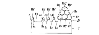
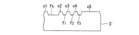
- the uneven substrate 1 has an uneven structure on one surface of the substrate. 5 and 6, an example in which a flat surface is provided between the convex portions will be described.
- the concavo-convex structure on the surface of the substrate has a large number of convex portions c1 to cn. Further, flat surfaces f1 to fn are formed between the respective convex portions. Note that n is a positive positive number.
- t1 to tn are the center points of the convex portions c1 to cn. Based on the measurement result of the AFM (atomic force microscope), a plurality of contour lines are drawn for each convex portion every 20 nm in parallel with the reference plane, and the center of gravity (point determined by the x and y coordinates) of each contour line is obtained. .
- the average position of these barycentric points is the center point of the convex portion.
- m1 to mn are the midpoints of adjacent center points obtained by AFM.
- the flat surfaces f1 to fn are based on the measurement result of AFM, and the inclination of the straight line connecting the surface height at the midpoint in the region and the surface height of any point in the region with respect to the reference surface of the AFM is This is an area that is ⁇ 10 ° or less.
- each flat surface f1 to fn is a distance of 2 to 300 nm from each midpoint m1 to mn when the most frequent pitch P of the concavo-convex structure is 1 ⁇ m or less.
- the distance is 5 to 100 nm.
- the distance from each midpoint m1 to mn is preferably 100 to 3000 nm, and more preferably 200 to 2000 nm.
- each flat surface and each midpoint is equal to or more than the preferred lower limit, a sufficient flat surface area as a substrate for a semiconductor light emitting device is secured, and the semiconductor layer can be easily and stably grown on the substrate. . Further, if the distance between the periphery of each flat surface and each midpoint is equal to or less than the preferable upper limit value, it is easy to obtain the effect of improving the light extraction efficiency by forming convex portions with sufficient density. Since the concavo-convex substrate 1 is not limited to a semiconductor light emitting device substrate, the distance from each midpoint m1 to mn to the periphery of each flat surface f1 to fn may be smaller than the lower limit value of the preferred range. Further, the flat surface may not exist.
- the convex part As the shape of the convex part, a cone, a truncated cone, a bamboo shoot shape or hemisphere with a conical slope bulging outward, a shape with a truncated cone slope bulging outward (a shape obtained by cutting the top of a bamboo shoot or hemisphere) ) And the like.
- the most frequent pitch P of the concavo-convex structure is preferably 100 nm to 5 ⁇ m, more preferably 100 nm to 1 ⁇ m, further preferably 200 nm to 700 nm, and particularly preferably 300 nm to 600 nm. If the most frequent pitch P is within a preferable range, it is easy to prevent total reflection of light.
- the most frequent pitch P is 1 ⁇ m or less, it is possible to more effectively increase the light extraction efficiency of blue to ultraviolet light. Therefore, it is suitable as a concavo-convex structure of a substrate used for a semiconductor light emitting device having a light emission wavelength in a blue to ultraviolet region by forming a film of GaN or InGaN.
- the most frequent pitch P is obtained as follows. First, in a randomly selected region on the concavo-convex surface, a surface parallel to the substrate surface in a square region 30 to 40 times the most frequent pitch P on which one side is predicted is defined as an AFM reference surface. AFM image is obtained. For example, when the most frequent pitch is about 300 nm, an image of an area of 9 ⁇ m ⁇ 9 ⁇ m to 12 ⁇ m ⁇ 12 ⁇ m is obtained. Then, this image is waveform-separated by Fourier transform to obtain an FFT image (fast Fourier transform image). Next, the distance from the zero-order peak to the primary peak in the profile of the FFT image is obtained.
- FFT image fast Fourier transform image
- the reciprocal of the distance thus obtained is the most frequent pitch P in this region.
- Such a process is similarly performed for a total of 25 or more regions of the same area selected at random, and the most frequent pitch in each region is obtained.
- the average value of the most frequent pitch P 1 ⁇ P 25 in 25 locations or more regions thus obtained is the most frequent pitch P.
- the regions are preferably selected at least 1 mm apart, more preferably 5 mm to 1 cm apart.
- the most frequent height H of the convex portion is preferably adjusted between 50 nm and 5 ⁇ m. If the most frequent height H is within a preferable range, film formation defects of a nitride compound formed thereafter can be reduced, and further, total reflection of light can be prevented and light extraction efficiency can be improved. Specifically, the most frequent height H of the convex portion is obtained as follows. First, a cross section as shown in FIG. 5 along a line having a length of 1 mm in an arbitrary direction and position is obtained from the AFM image.
- the concavo-convex substrate 1 does not have a convex portion that is 30 nm or more higher than the most frequent height H of the convex portion.
- an AFM image of 20 ⁇ m in length ⁇ 20 ⁇ m in width of the concavo-convex substrate 1 is measured at 5 ⁇ 5 places (25 places) at intervals of 1 mm in length and width, and more than a predetermined height from the most frequent height H of the convex portions.
- the concavo-convex substrate 1 has a plurality of areas C 1 to C n as shown in FIG.
- Each of the areas C 1 to C n is an area in which the center points of the seven adjacent convex portions are continuously aligned in a positional relationship where the six vertexes of the regular hexagon and the diagonal lines intersect.
- FIG. 6 the position of the center point of each convex portion is indicated by a circle u centered on the center point for convenience. As shown in FIG. 5, the circle u corresponds to a region including not only each convex portion but also a flat surface around it.
- the positional relationship in which the center points of the seven adjacent convex portions are the intersections of the six apexes of the regular hexagon and the diagonal line specifically refers to a relationship satisfying the following conditions.
- a line segment L1 having a length equal to the most frequent pitch P is drawn from one center point t1 in the direction of the adjacent center point t2.
- line segments L2 to L6 having a length equal to the most frequent pitch P are drawn from the center point t1 in directions of 60 °, 120 °, 180 °, 240 °, and 300 ° with respect to the line segment L1.
- center points adjacent to the center point t1 are within 15% of the most frequent pitch P from the end points of the line segments L1 to L6 on the side opposite to the center point t1, these seven center points are It is in a positional relationship that is the intersection of six vertices of a regular hexagon and a diagonal line.
- the mode Q of each area C 1 to C n (the mode value of each area) is preferably in the following range.
- the mode area Q in the 10 mm ⁇ 10 mm AFM image measurement range is preferably 0.026 ⁇ m 2 to 6.5 mm 2 .
- the mode area Q in the 10 mm ⁇ 10 mm AFM image measurement range is preferably 0.65 ⁇ m 2 to 26 mm 2 .
- the mode area Q in the AFM image measurement range of 50 mm ⁇ 50 mm is preferably 2.6 ⁇ m 2 to 650 mm 2 . If the most frequent area Q is within a preferable range, it is easy to prevent problems such as light color shift and in-plane anisotropy.
- Each area C 1 to C n is random in area, shape, and lattice orientation, as shown in FIG. Specifically, the degree of randomness of the area preferably satisfies the following conditions.
- an ellipse having the maximum area circumscribed by the boundary line of one area is drawn, and the ellipse is expressed by the following formula ( ⁇ ).
- X 2 / a 2 + Y 2 / b 2 1... ( ⁇ )
- the standard deviation of ⁇ ab within the 10 mm ⁇ 10 mm AFM image measurement range is preferably 0.08 ⁇ m 2 or more.
- the standard deviation of ⁇ ab within the AFM image measurement range of 10 mm ⁇ 10 mm is preferably 1.95 ⁇ m 2 or more.
- the standard deviation of ⁇ ab in the 50 mm ⁇ 50 mm AFM image measurement range is preferably 8.58 ⁇ m 2 or more. If the standard deviation of ⁇ ab is within a preferable range, the effect of averaging the diffracted light is excellent.
- the degree of randomness of the shapes of the areas C 1 to C n is specifically, the ratio of a to b in the formula ( ⁇ ), and the standard deviation of a / b is 0.1 or more. preferable.
- the randomness of the lattice orientation of each area C 1 to C n preferably satisfies the following conditions. First, a straight line K0 connecting the center points of any two adjacent convex portions in any area (I) is drawn. Next, one area (II) adjacent to the area (I) is selected, and six protrusions in the area (II) are connected to the center points of the six protrusions adjacent to the protrusion. Draw the straight lines K1 to K6.
- the straight lines K1 to K6 are at angles different from each other by 3 degrees or more with respect to the straight line K0, it is defined that the lattice orientations of the area (I) and the area (II) are different.
- the areas adjacent to the area (I) there are preferably two or more areas having a lattice orientation different from the lattice orientation of the area (I), preferably 3 or more, and more preferably 5 or more.
- the concavo-convex structure of the concavo-convex substrate 1 is a so-called polycrystalline structure in which the lattice orientation is aligned within each of the areas C 1 to C n but not macroscopically.
- the randomness of the macroscopic lattice orientation can be evaluated by the ratio between the maximum value and the minimum value of the FFT (Fast Fourier Transform) fundamental wave.
- the ratio between the maximum value and the minimum value of the FFT fundamental wave is obtained by acquiring an AFM image, obtaining a two-dimensional Fourier transform image thereof, and drawing a circle away from the origin by the wave number of the fundamental wave.
- the point having the largest amplitude and the point having the smallest amplitude are extracted and obtained as a ratio of the amplitudes.
- the method for acquiring the AFM image at this time is the same as the method for acquiring the AFM image when obtaining the most frequent pitch P.
- the concavo-convex structure having a large ratio between the maximum value and the minimum value of the FFT fundamental wave has a uniform lattice orientation, and when the concavo-convex structure is regarded as a two-dimensional crystal, it can be said to be a structure having high single crystallinity.
- the concavo-convex structure having a small ratio between the maximum value and the minimum value of the FFT fundamental wave has a non-uniform lattice orientation, and can be said to be a polycrystalline structure when the concavo-convex structure is regarded as a two-dimensional crystal.
- the concavo-convex structure of the concavo-convex substrate 1 has a ratio between the maximum value and the minimum value of the FFT fundamental wave in the preferable range, diffracted light is not emitted in a specific in-plane direction, and diffracted light is emitted evenly.
- the radiation intensity of the light emitting diode does not vary depending on the viewing angle.
- a semiconductor light emitting device having low in-plane radiation anisotropy can be obtained.
- the light-emitting diode has a phosphor layer for converting the wavelength of light from the light-emitting layer
- the light from the light-emitting layer is wavelength-converted by the phosphor, and then the light is re-emitted in the light-emitting diode element.
- the diffracted light overlaps the original spectrum, resulting in an increase in specific wavelength.
- the bottom emission in which a reflective electrode is provided on the upper surface and ultraviolet light is converted into white by the three primary color phosphors.
- Type white LED If the concavo-convex structure has a ratio between the maximum value and the minimum value of the FFT fundamental wave in the above preferable range, the angle at which the diffracted light is emitted can be prevented from being biased, and color shift can be suppressed.
- the concavo-convex substrate 1 has an appropriate concavo-convex structure and randomness. Therefore, sufficient light extraction efficiency can be obtained, and the problem of high color shift and in-plane anisotropy can be prevented by averaging the diffracted light.
- the method for producing a concavo-convex substrate according to the present invention includes a particle arranging step in which a plurality of particles are arranged in a substantially single layer on the original plate, dry etching the original plate using the plurality of particles as an etching mask, and a concavo-convex structure on one surface of the original plate An etching process to be formed and a removing process to remove a plurality of particles remaining on the formed uneven structure are provided.
- each process will be sequentially described with reference to FIGS. 1 to 3D. 2A to 3D, for convenience of explanation, the unevenness formed on the particles M and the original plate S is extremely enlarged.
- the particle arranging step is performed by a method using a so-called LB method (Langmuir-Blodgett method). Specifically, it comprises a dropping step of dropping a dispersion liquid in which particles are dispersed in a solvent having a specific gravity smaller than that of water on the surface of the water in the water tank, and volatilizing the solvent from the dropped dispersion liquid.
- the particle arranging step is performed by a method having a single particle film forming step for forming a single particle film and a transfer step for transferring the single particle film to an original plate. This method combines the accuracy of monolayering, the ease of operation, the response to large areas, and reproducibility.
- the dispersion liquid is prepared by adding particles M in a solvent having a specific gravity smaller than that of water.
- a water tank trough
- water for developing the particles M on the liquid surface hereinafter sometimes referred to as lower layer water
- the particle M preferably has a hydrophobic surface. Further, it is preferable to select a hydrophobic solvent. By combining the hydrophobic particles M and the solvent with the lower layer water, as will be described later, self-organization of the particles M proceeds, and a two-dimensional close-packed single particle film is formed. It is also important that the solvent has high volatility.
- the volatile and hydrophobic solvent includes one or more volatile organic solvents such as chloroform, methanol, ethanol, isopropanol, acetone, methyl ethyl ketone, ethyl ethyl ketone, toluene, hexane, cyclohexane, ethyl acetate, and butyl acetate. Is mentioned.
- the surface thereof is usually hydrophilic, so that it is preferably used after being hydrophobized with a hydrophobizing agent.
- a hydrophobizing agent for example, a surfactant, a metal alkoxysilane, or the like can be used.
- Hydrophobization of the particles M can be performed by the same method using a surfactant, metal alkoxysilane, and the like similar to the hydrophobizing agent described in JP2009-162831A.
- the dispersion before dropping onto the liquid surface is microfiltered with a membrane filter or the like, and aggregated particles (from a plurality of primary particles) present in the dispersion are used. Secondary particles) are preferably removed. If the microfiltration is performed in advance as described above, it is difficult to generate a portion where two or more layers are formed or a defective portion where particles are not present, and it is easy to obtain a single particle film with high accuracy. If the formed single particle film has a defect portion having a size of several to several tens of ⁇ m, it is difficult to obtain a highly accurate single particle film.
- an LB trough device having a surface pressure sensor for measuring the surface pressure of the single particle film and a movable barrier for compressing the single particle film in the liquid surface direction was used in a transition process described in detail later.
- the dispersion liquid demonstrated above is dripped at the liquid level of lower layer water (drip process). Then, the solvent as the dispersion medium is volatilized, and the particles M are developed as a single layer on the liquid surface of the lower layer water to form a two-dimensional close packed single particle film (single particle film formation). Process).
- the particle concentration of the dispersion dropped into the lower layer water is preferably 1 to 10% by mass.
- the dropping rate is preferably 0.001 to 0.01 ml / second. If the concentration of the particles M in the dispersion and the amount of dripping are in such a range, the particles partially agglomerate in a cluster to form two or more layers, resulting in defective portions where no particles are present, and the pitch between the particles. The tendency to spread is suppressed. Therefore, it is easier to obtain a single particle film in which each particle is two-dimensionally closely packed with high accuracy.
- a single particle film is formed by self-organization of the particles M.
- the principle is that when the particles are aggregated, surface tension acts due to the dispersion medium existing between the particles.
- the particles M do not exist at random, but have a two-dimensional close packed structure. It forms automatically.
- the close-packing by surface tension can be said to be arrangement by lateral capillary force.
- three particles M having a spherical shape and high particle size uniformity, such as colloidal silica are brought together in contact with each other while floating on the water surface, the total length of the water line of the particle group is minimized. Surface tension acts. Therefore, as shown in FIG. 1, the three particles M are stabilized in an arrangement based on an equilateral triangle indicated by T in the figure.
- the single particle film forming step is preferably performed under ultrasonic irradiation conditions.
- the solvent of the dispersion liquid is volatilized while irradiating ultrasonic waves from the lower layer water to the water surface, the closest packing of particles M is promoted, and each particle M is more densely packed in two dimensions with a single particle film. Is obtained.
- the output of the ultrasonic wave is preferably 1 to 1200 W, and more preferably 50 to 600 W.
- the frequency of the ultrasonic wave is not particularly limited, but is preferably, for example, 28 kHz to 5 MHz, and more preferably 700 kHz to 2 MHz.
- the frequency is too high, energy absorption of water molecules begins, and a phenomenon in which water vapor or water droplets rise from the water surface is not preferable.
- the frequency is too low, the cavitation radius in the lower layer water becomes large, bubbles are generated in the water, and rise toward the water surface. If such bubbles accumulate under the single particle film, the flatness of the water surface is lost, which is inconvenient.
- a standing wave is generated on the water surface by ultrasonic irradiation. If the output is too high at any frequency, or if the wave height of the water surface becomes too high due to the tuning conditions of the ultrasonic transducer and the transmitter, the single particle film will be destroyed by the water surface wave, so care must be taken.
- the ultrasonic frequency and output are appropriately set in consideration of the above, close-packing of particles can be effectively promoted without destroying the single particle film being formed.
- the natural frequency calculated from the particle size of the particles should be used as a guide.
- the particle diameter is small, for example, 100 nm or less, the natural frequency becomes very high, and it is difficult to apply ultrasonic vibration as calculated.
- the necessary frequency can be reduced to a practical range.
- the ultrasonic irradiation time may be sufficient to complete the rearrangement of particles, and the required time varies depending on the particle size, ultrasonic frequency, water temperature, and the like.
- the normal production conditions are preferably 10 seconds to 60 minutes, more preferably 3 minutes to 30 minutes.
- the advantage obtained by ultrasonic irradiation is the effect of destroying the soft agglomerates of particles that are likely to occur when preparing a dispersion of nanoparticles, in addition to the closest packing of particles (to make the random array 6-way closest) The generated point defects, line defects, crystal transitions and the like are also repaired to some extent.
- the single particle film formed on the liquid surface by the single particle film forming step is transferred to the original plate S in a single layer state (transfer step).
- transfer step There is no particular limitation on the specific method of transferring the single particle film to the original plate S.
- the hydrophobic original plate S is lowered from above and brought into contact with the single particle film.
- a method of transferring the particle film to the original plate S and transferring it can be adopted.
- the original plate S in a substantially horizontal direction in the lower layer water of the water tank in advance before forming the single particle film, and gradually lowering the liquid level after forming the single particle film on the liquid surface, A method of transferring the single particle film to the original plate S can also be adopted. According to these methods, the single particle film can be transferred to the original plate S without using a special apparatus. However, it is preferable to adopt a so-called LB trough method in the transition process (see Journal of Materials and Chemistry, Vol. 11, 3333 (2001), Journal of Materials and Chemistry, Vol. 12, 3268 (2002)). ).
- a single particle film can be transferred to the original plate S without using a special apparatus, but also a secondary close-packing of a single particle film of a larger area. It is easy to transfer to the original plate S while maintaining the state.
- FIG. 2A and 2B schematically show an outline of the LB trough method.
- the particle M is extremely enlarged for convenience of explanation.
- the original plate S is preliminarily immersed in the lower layer water W in the water tank V, and the above-described dropping step and single particle film forming step are performed in this state to form the single particle film F ( FIG. 2A).
- the single particle film F can be transferred to the original plate S by pulling the original plate S upward while maintaining the substantially vertical direction (FIG. 2B).
- the single particle film F is the original plate S. It may be transferred only to the flat surface X.
- the single particle film F is formed only on the flat surface X while preventing the particles M from wrapping around from the flat surface X side to the back surface. Transfer is preferable because the single particle film F can be transferred more precisely. However, it can be transferred to both sides.
- the temperature condition of the transition step (temperature of the lower layer water), the pulling speed of the original plate S, etc. Even if it fluctuates somewhat, there is no fear that the single particle film F collapses and becomes multi-layered in the transfer step.
- the temperature of the lower layer water is usually about 10 to 30 ° C. depending on the environmental temperature which varies depending on the season and weather.
- a surface pressure sensor based on an unillustrated Wilhelmy plate or the like that measures the surface pressure of the single particle film F, and an illustration that compresses the single particle film F in the direction along the liquid surface. It is preferred to use an LB trough device with an approximate movable barrier. Thereby, the single particle film F having a larger area can be transferred to the original plate S more stably. According to such an apparatus, the single particle film F can be compressed to a preferable diffusion pressure (density) while measuring the surface pressure of the single particle film F, and is moved toward the original plate S at a constant speed. be able to.
- a preferable diffusion pressure is 5 to 80 mNm ⁇ 1 , more preferably 10 to 40 mNm ⁇ 1 . With such a diffusion pressure, it is easy to obtain a single particle film F in which each particle is two-dimensionally closely packed with higher accuracy.
- the speed at which the original sheet S is pulled up is preferably 0.5 to 20 mm / min.
- the temperature of the lower layer water is usually 10 to 30 ° C. as described above. Note that the LB trough device can be obtained as a commercial product.
- the single particle film F of the particles M can be transferred to the original plate S by the transfer step, but a fixing step for fixing the transferred single particle film F to the original plate S may be performed after the transfer step.
- a fixing step for fixing the transferred single particle film F to the original plate S may be performed after the transfer step.
- a method using a binder and a sintering method there are a method using a binder and a sintering method.
- a binder solution is supplied to the flat surface X side of the original plate S on which the single particle film is formed, and this is infiltrated between the particles M constituting the single particle film and the original plate S.
- the amount of the binder used is preferably 0.001 to 0.02 times the mass of the single particle film. If it is such a range, there will be too much binder and a binder will be clogged between particle
- the excess of the binder solution may be removed by using a spin coater or tilting the original plate S.
- the binder metal alkoxysilanes, general organic binders, inorganic binders and the like exemplified above as the hydrophobizing agent can be used.
- heat treatment may be appropriately performed depending on the type of the binder. .
- the original plate S on which the single particle film is formed may be heated to fuse each particle M constituting the single particle film to the original plate S.
- the heating temperature may be determined according to the material of the particle M and the material of the original plate S. However, since the particle M having a particle size of 1 ⁇ m ⁇ or less starts an interfacial reaction at a temperature lower than the original melting point of the material, the heating temperature is relatively low. Sintering is complete on the side. If the heating temperature is too high, the fusion area of the particles increases, and as a result, the shape of the single particle film may change, which may affect the accuracy. In addition, if heating is performed in air, the original plate S and each particle M may be oxidized.
- the original plate S may be sapphire, SiC, Si, MgAl 2 O 4 , LiTaO 3 , ZrB 2 , CrB 2 or the like.
- plate material which consists of these materials can be used.
- sapphire is preferable in terms of mechanical stability, thermal stability, optical stability, and chemical stability.
- the base plate S provided with a concavo-convex structure is used as a substrate of a bottom emission type organic light emitting diode as it is, a transparent body that transmits visible light is used as the base plate S so that light can be extracted from the substrate.
- the original plate S one having a transmittance of 70% or more, preferably 80% or more, and more preferably 90% or more without giving a bias to the spectrum in the visible light range (wavelength 380 nm to 800 nm).
- the material of the original plate S that is a transparent body may be an inorganic material, an organic material, or a combination thereof.
- the inorganic material examples include various glasses such as quartz glass, alkali-free glass, white plate glass, and transparent inorganic minerals such as mica.
- the organic material examples include a resin film such as a cycloolefin film and a polyester film, and a fiber reinforced plastic material in which fine fibers such as cellulose nanofiber are mixed in the resin film.
- the original plate S When a substrate provided with a concavo-convex structure on the original plate S is used as it is as a substrate of a top emission type organic light emitting diode, the original plate S does not necessarily have to be transparent because light is extracted from the side opposite to the substrate. Therefore, the same material as that for the substrate of the bottom emission type organic light emitting diode can be used, and for example, a metal plate such as a stainless plate or a copper plate, a silicon wafer, or the like can be used.
- a metal plate such as a stainless plate or a copper plate, a silicon wafer, or the like is used. Can do.
- particles M examples include inorganic particles such as metals and metal oxides, and organic polymers such as polystyrene and polymethyl methacrylate. These may be used alone or in combination of two or more. By selecting the material of the particles M and the dry etching conditions described later, the height and shape of the concavo-convex structure to be formed can be adjusted.
- the particles M are preferably inorganic particles.
- the inorganic particles for example, particles composed of oxides, nitrides, carbides, borides, sulfides, selenides, metals and the like, metal particles, and the like can be used.
- oxides examples include silica, alumina, zirconia, titania, ceria, zinc oxide, tin oxide, and yttrium aluminum garnet (YAG). Further, these constituent elements are partially substituted with other elements. Can also be used.
- nitride examples include silicon nitride, aluminum nitride, boron nitride, and the like, and those obtained by partially replacing these constituent elements with other elements can also be used.
- a compound such as sialon composed of silicon, aluminum, oxygen, and nitrogen can also be used.
- carbide examples include SiC, boron carbide, diamond, graphite, fullerenes, and those in which these constituent elements are partially substituted with other elements can also be used.
- Examples of the boride that can be used include ZrB 2 , CrB 2, and the like, and those obtained by partially substituting these constituent elements with other elements can also be used.
- Examples of the sulfide that can be used include zinc sulfide, calcium sulfide, cadmium sulfide, strontium sulfide, and the like, and those obtained by partially replacing these constituent elements with other elements can also be used.
- Examples of the selenide that can be used include zinc selenide, cadmium selenide, and the like, and those obtained by partially substituting these constituent elements with other elements can also be used.
- As the metal that can be used particles made of one or more metals selected from the group consisting of Si, Ni, W, Ta, Cr, Ti, Mg, Ca, Al, Au, Ag, and Zn are used. Can do.
- Each of the inorganic particles can be used alone as the particle M, or a mixture of these inorganic particles can be used as the particle M.
- coated particles such as inorganic particles made of nitride coated with an oxide can be used as the particles M.
- phosphor particles obtained by introducing an activator such as cerium or europium into the inorganic particles can be used as the particles M.
- oxides are preferable in terms of shape stability, and silica is more preferable among them.
- a plurality of particles M are arranged in a substantially single layer on the flat surface X which is one surface of the original plate S by the particle arranging step. That is, the single particle film F of the particles M is formed on the flat surface X.
- the particle arranging step it is preferable to arrange a plurality of particles M on the original plate S in a single layer so that the deviation D (%) of the arrangement defined by the following formula (1) is 15% or less.
- D [%]
- A is the average particle diameter of the particle
- B is the most frequent pitch between the particle
- the deviation D is preferably 10% or less, and more preferably 1.0 to 3.0%.
- the average particle size A of the particles M is the average primary particle size of the particles M constituting the single particle film, and the particle size distribution obtained by the particle dynamic light scattering method is fitted to a Gaussian curve. It can obtain
- the pitch between the particles M is the distance between the vertices of two adjacent particles M in the sheet surface direction, and the most frequent pitch B is an average of these. If the particles M are spherical, the distance between the vertices of the adjacent particles M is equal to the distance between the centers of the adjacent particles M.
- the most frequent pitch B between the particles M is obtained as follows. First, an atomic force microscope image of a randomly selected region in a single particle film with a side parallel to the sheet surface 30 to 40 times the predicted mode pitch B between the particles M is obtained. obtain. For example, in the case of a single particle film using particles M having a particle size of 300 nm, an image of a region of 9 ⁇ m ⁇ 9 ⁇ m to 12 ⁇ m ⁇ 12 ⁇ m is obtained. Then, this image is waveform-separated by Fourier transform to obtain an FFT image (fast Fourier transform image). Next, the distance from the zero-order peak to the primary peak in the profile of the FFT image is obtained.
- FFT image fast Fourier transform image
- the reciprocal of the distance thus obtained is the most frequent pitch B 1 in this region.
- Such processing is similarly performed for a total of 25 or more regions having the same area selected at random, and the most frequent pitches B 1 to B 25 in each region are obtained.
- the average value of the most frequent pitches B 1 to B 25 in the 25 or more regions thus obtained is the most frequent pitch B in the equation (1).
- the regions are preferably selected at least 1 mm apart, more preferably 5 mm to 1 cm apart.
- the variation in pitch between the particles M in each image can be evaluated from the area of the primary peak in the profile of the FFT image.
- This misalignment D is an index indicating the degree of closest packing of the particles M. That is, a small deviation D of the arrangement of particles means that the degree of close-packing is high, the interval between the particles is controlled, and the accuracy of the arrangement is high.
- the coefficient of variation of the particle size of the particles M is preferably 20% or less, and preferably 10% or less. More preferably, it is 5% or less.
- the pitch of the concavo-convex structure provided on the original plate S according to the present invention is equivalent to the most frequent pitch B between the particles M.
- the pitch of the concavo-convex structure is substantially equal to the average particle diameter A of the particles M. Therefore, by appropriately selecting the average particle diameter A of the particles M, a desired pitch can be obtained.
- the uneven structure can be formed with high accuracy.
- the particles M can be easily arranged so that the deviation D is 15% or less by the particle arranging step of the present invention. That is, an etching mask in which particles M are closely packed with a single layer can be arranged on the original plate S with very high accuracy.
- a portion where the particle M does not cover the original plate S and a portion where the particle M overlaps are generated only slightly by the particle arranging step of the present invention.
- the frequency per unit area of the portion where the particles overlap is 1 to 1000 locations / mm 2 .
- the case where the particles are overlapped to this extent is called a substantially single layer.
- FIG. 3A is a diagram showing a state of a portion where such a slight defect occurs after the particle arranging step. That is, in FIG. 3A, particles M1 to M10 (a plurality of particles M) are arranged on the flat surface X of the original plate S. The arrangement of the particles M1 to M10 is defective at the following two points. a. There is a portion where the flat surface X is not covered with the particles M between the particles M1 and the particles M2. b. The particles M8 to M10 are superposed on the particles M5 to M7.
- FIG. 3B shows changes in the particles M and the original plate S when this dry etching process is performed in the following two stages (S1) and (S2). If the flat surfaces f1 to fn described in FIG. 5 are not necessary, the step (S1) is not necessary.
- S1 A step of dry etching the particles M under the condition that the particles M are etched and the original plate S is not substantially etched.
- S2 A step of dry-etching the original plate S using the particles remaining in (S1) as an etching mask under conditions where both the particles M and the original plate S are substantially etched.
- an etching gas may be appropriately selected.
- the original plate S is sapphire and the particle M is silica
- one or more selected from CF 4 , SF 6 , CHF 3 , C 2 F 6 , C 3 F 8 , CH 2 F 2 , and NF 3 Dry etching is preferably performed using this gas.
- the particles M can be etched with little influence on the original plate S.
- the etching step (S1) needs to be performed so that particles functioning as an etching mask remain in the etching step (S2).
- the size of the particle M in the surface direction (horizontal direction) of the original plate S (hereinafter referred to as the “height”) is maintained while maintaining a sufficient diameter (hereinafter referred to as “height”) of the particles M in the thickness direction (vertical direction) of the original plate S.
- the bias power may be set low or the pressure may be reduced.
- the etching step (S2) is preferably performed under the condition that the dry etching selectivity of the above formula (2) is greater than 100%, more preferably 200% or more, and even more preferably 300% or more.
- an etching gas may be appropriately selected according to the material of the original plate S and the particles M.
- the original plate S is quartz and the particles M are colloidal silica
- Ar, CF 4 or the like can be used.
- dry etching may be performed using one or more gases selected from Cl 2 , BCl 3 , SiCl 4 , HBr, HI, and HCl.
- a reactive ion etching apparatus As an etching apparatus that can be used in the etching steps (S1) and (S2), a reactive ion etching apparatus, an ion beam etching apparatus, or the like, which can perform anisotropic etching, has a minimum bias electric field of about 20 W. As long as it can generate. There are no particular restrictions on the specifications such as the plasma generation method, electrode structure, chamber structure, and frequency of the high-frequency power source.
- the particles M arranged in a single layer such as the particles M2 to M4, are etched to become small, and a gap is generated therebetween.
- the particles M1 and M10 are also etched and reduced in the same manner as the particles M2 to M4.
- the particles M5 to M9 are masked by the particles superposed on the upper side, the degree of etching is limited.
- the original plate S is dry-etched using the particles remaining in the step (S1) as an etching mask.
- Etching of the flat surface X proceeds while maintaining a substantially flat surface in a gap portion formed by etching and reducing the particles M arranged in a single layer, such as the particles M2 to M4. Further, on the lower flat surface X of the remaining particles M1 to M4, as each particle M is gradually etched to become smaller, it gradually goes from the lower portion around each particle M toward the lower portion in the center. Since the etching progresses, the etching surface becomes inclined. On the other hand, the particles M1 are further etched, but the particles M5 to M9 are limited in the degree of etching because the upper overlapping particles serve as a mask. Under the particles M5 to M10, the etching of the flat surface X hardly proceeds.
- the etching process is terminated before the particles M1 to M4 arranged in a substantially single layer disappear.
- the particles M1 to M4 and M10 become particles M1 ′ to M4 ′ and M10 ′ having small particle diameters.
- the portions of the particles M5 to M9 that are masked by the overlapping particles remain, and become particles M5 ′ to M9 ′ as shown in FIG. 3B. Further, an etching residue Mx is deposited around each remaining particle.
- the etching process may be completed so that the volume of the particles M1 ′ to M4 ′ and M10 ′ at the end of the etching process is about 10 to 90% of the volume of the particles M1 to M4 and M10.
- the etching process may be terminated so that the mass ratio of the particles M1 ′ to M4 ′ and M10 ′ and the particles M1 to M4 and M10 at the end of the etching process is 1: 1.1 to 1: 100.
- the etching process may be terminated by setting conditions such that the step is completed with an etching time that provides a target uneven structure step, for example, a step of 10 nm to 200 nm.
- the uneven structure of the original plate S ′ is completed.
- frustoconical convex portions c1 to c4 having the top surfaces of the remaining particles M1 ′ to M4 ′ are formed.
- a convex portion c5 having a wide top surface is formed below the particles M5 to M10.
- the particles M are etched and reduced in the step (S1).
- the flat surfaces f1 to f3 are formed corresponding to the generated gap portions.
- a coarse flat surface fx is formed between the convex part c1 and the convex part c2. If the step (S1) is omitted, the flat surfaces f1 to f3 are not formed.
- the pitch of the concavo-convex structure formed on the original plate S ′ is equivalent to the most frequent pitch B between the particles M described above. Since the arrangement of the particles M in FIG. 3A has a high degree of fine packing, by appropriately selecting the average particle diameter A of the particles M, it is possible to accurately form an uneven structure with a desired pitch.
- the shape of the normally formed convex portions c1 to c4 is not limited to a strict truncated cone, but may be a bamboo shoot shape whose side surface bulges outward or a hemispherical convex portion cut by a plane parallel to the bottom surface. .
- the shape of the projections c1 to c4 can be adjusted by the bias power, the pressure in the vacuum chamber, and the type of etching gas. For example, if the pressure is lowered, the shape has a gentle inclination angle.
- the flat surfaces f1 to f3 are kept flat as the dry etching selectivity in the step (S1) is lower. It is preferable that the gap between the convex portions be a flat surface because the film forming property of a layer to be subsequently laminated on the substrate is improved.
- the remaining particles M are removed.
- the particles M can be removed by a chemical removal method using an etchant having an etching property with respect to the particles M and an etching resistance with respect to the original plate S ′, or a physical removal method using a brush roll cleaning machine or the like. Since the etching process is completed before the particles M arranged in a single layer disappear, the adhesion force of the etching residue Mx is not strong, and the etching residue Mx can also be removed by the above-described normal chemical removal method or physical removal method. . Thereby, an original plate S ′ having a concavo-convex structure shown in FIG. 3C is obtained.
- the original plate S ′ does not have a convex portion (spike) protruding from the apex, including the convex portion c5.
- Spikes are considered to cause defects in the layers stacked on the substrate, which in turn cause defects due to short circuits and problems of reduced life.
- the presence of the convex portion c5 having a wide top surface and the coarse flat surface fx does not cause a defect of a layer laminated on the substrate like a spike.
- the convex portion c5 and the coarse flat surface fx (lack of the convex portion) are factors that reduce the light extraction efficiency improvement effect, but are very slight from the viewpoint of the light extraction efficiency improvement effect obtained as a whole. It will not be a trap.
- the convex portions c1 to c5 are further digged into the slopes of the bottoms to become convex portions c1 ′ to c5 ′.
- 'flat surfaces f1 to f3 become further dug flat surfaces f1' to f3 '
- coarse flat surface fx becomes further dug deep flat surface fx'.
- the fixed object cx is strongly fixed on the convex part c5 ′. Therefore, it is difficult to remove the fixed substance cx at this stage by a normal chemical removal method or physical removal method. As a result, in the obtained original plate Sx, a spike in which the convex portion c5 ′ and the fixed object cx are superimposed is generated.
- the concavo-convex substrate of the present invention may be the original plate S itself after the removal step, or a concavo-convex substrate obtained by transferring the concavo-convex structure a plurality of times. That is, the manufacturing method of the concavo-convex substrate of the present invention may include a transfer step of transferring the concavo-convex structure provided on the original plate S after the removing step a plurality of times. By transferring a plurality of times, a concavo-convex substrate having a concavo-convex structure equivalent to the concavo-convex structure provided on the original plate S after the removing step is obtained.
- the transfer process By performing the transfer process, a plurality of concave and convex substrates can be efficiently manufactured.
- the concavo-convex structure of the original plate S after the removal process is transferred to a mold (mold or stamper) (first transfer), and then the concavo-convex structure of the mold is transferred (second transfer), and transferred twice. It is preferable that it is this process.
- an electroforming method as disclosed in, for example, Japanese Patent Application Laid-Open No. 2009-158478 is preferable.
- the method for transferring the concavo-convex structure of the mold include a nanoimprint method, a hot press method, an injection molding method, and a UV embossing method as disclosed in Japanese Patent Application Laid-Open No. 2009-158478.
- the nanoimprint method is suitable for transferring a fine uneven structure.
- the light-emitting diode (inorganic light-emitting diode) of the present invention includes the concavo-convex substrate of the present invention and a semiconductor functional layer laminated on the surface on which the concavo-convex structure of the concavo-convex substrate is formed.
- the semiconductor constituting the semiconductor functional layer is preferably a group III-V nitride semiconductor in which the group V element is nitrogen. This is because the group III-V nitride semiconductor needs to be formed on a substrate such as sapphire.
- the group III element is a group 13 element in IUPAC
- the group V element is a group 15 element in IUPAC.
- Typical group III-V nitride semiconductors are gallium nitride and indium nitride. Strictly speaking, aluminum nitride is an insulator, but in the present invention, it is treated as corresponding to a group III-V nitride semiconductor according to the practice of the light emitting diode field.
- the layer structure of the semiconductor functional layer is a structure necessary for the operation of the III-V nitride light emitting diode.
- the semiconductor functional layer has at least an n-type conductivity layer, a p-type conductivity layer, and a light emitting layer sandwiched therebetween, and is composed of a III-V group nitride semiconductor layer. Those are preferred.
- the III-V nitride semiconductor functional layer includes high-quality layers. It may include other layers necessary to make crystals.
- the other layer may be a single layer or a multilayer layer (including a thick film layer and a superlattice thin film layer).
- a buffer layer may be included as another layer.
- Each of the above layers may also be composed of a plurality of layers.
- Specific semiconductor functional layers include a buffer layer made of GaN, AlN, etc., an n-type conductive layer (clad layer) made of n-GaN, n-AlGaN, etc., a light emitting layer made of InGaN, GaN, etc.
- Examples include a multilayer film in which a p-type conductive layer (clad layer) made of undoped GaN, p-GaN, etc., and a cap layer made of Mg-doped AlGaN and Mg-doped GaN are sequentially stacked (for example, Japanese Patent Laid-Open No. Hei 6).
- electrodes made of a metal such as Ni, Au, Pt, Pd, Rh, Ti, and Al can be used as an n-type electrode and a p-type electrode for supplying current to the light emitting layer.
- electrodes made of a metal such as Ni, Au, Pt, Pd, Rh, Ti, and Al can be used as an n-type electrode and a p-type electrode for supplying current to the light emitting layer.
- the light-emitting diode (inorganic light-emitting diode) of the present invention has a semiconductor functional layer on a concavo-convex substrate on which a concavo-convex structure having a desired pitch is accurately formed. Therefore, sufficient light extraction efficiency can be obtained.
- the semiconductor functional layer is laminated on an uneven substrate without spikes, defects are unlikely to occur. As a result, the occurrence of defects due to short circuits and the problem of life reduction are improved.
- the method for producing a light emitting diode (inorganic light emitting diode) of the present invention comprises a step of obtaining a concavo-convex substrate by the method for producing a concavo-convex substrate of the present invention, and at least a light emitting layer on the surface on which the concavo-convex structure of the obtained concavo-convex substrate is formed.
- a laminating step of laminating a semiconductor functional layer comprises a step of obtaining a concavo-convex substrate by the method for producing a concavo-convex substrate of the present invention, and at least a light emitting layer on the surface on which the concavo-convex structure of the obtained concavo-convex substrate is formed.
- a known epitaxial growth method such as MOVPE method (metal organic vapor phase epitaxy), MBE method (molecular beam epitaxy method), HVPE method (hydride vapor phase epitaxy) can be used.
- MOVPE method metal organic vapor phase epitaxy
- MBE method molecular beam epitaxy method
- HVPE method hydrogen vapor phase epitaxy
- Group III materials include general formulas such as trimethylgallium [(CH 3 ) 3 Ga, hereinafter sometimes referred to as TMG] and triethylgallium [(C 2 H 5 ) 3 Ga, hereinafter sometimes referred to as TEG].
- Trialkylgallium represented by R 1 R 2 R 3 Ga (where R 1 , R 2 and R 3 represent lower alkyl groups), trimethylaluminum [(CH 3 ) 3 Al, hereinafter referred to as TMA
- R 1 R 2 R 3 such as triethylaluminum [(C 2 H 5 ) 3 Al, hereinafter sometimes referred to as TEA], triisobutylaluminum [(i-C 4 H 9 ) 3 Al]
- Trialkylaluminum represented by Al (wherein R 1 , R 2 and R 3 represent lower alkyl groups), trimethylamine alane [(CH 3 ) 3 N: AlH 3 ], trimethylindium [(CH 3 ) 3 In, hereinafter sometimes referred to as TMI], and general formulas R 1 R 2 R 3 In (where R 1 , R 2 , R 3 are such as triethylindium [(C 2 H 5 ) 3 In])
- Group V raw material examples include ammonia, hydrazine, methyl hydrazine, 1,1-dimethylhydrazine, 1,2-dimethylhydrazine, t-butylamine, and ethylenediamine. These can be used alone or in any combination. Among these raw materials, ammonia and hydrazine are preferable because they do not contain carbon atoms in their molecules and thus cause less carbon contamination in the semiconductor.
- gases such as nitrogen, hydrogen, argon, and helium can be used singly or as a mixture, and hydrogen and helium are preferred as the growth atmosphere gas and the carrier gas of the organometallic raw material.
- the semiconductor functional layer is laminated on the concavo-convex substrate on which the concavo-convex structure having a desired pitch is accurately formed. Therefore, a light-emitting diode that can obtain sufficient light extraction efficiency can be obtained.
- the semiconductor functional layer is stacked on the uneven substrate without spikes, it is possible to obtain a light emitting diode in which defects in the semiconductor functional layer are less likely to be generated, and as a result, the occurrence of defects due to short circuits and the problem of life reduction are improved.
- the light-emitting diode (organic light-emitting diode) according to the present invention includes a concavo-convex substrate according to the present invention, an anode conductive layer provided on a surface on which the concavo-convex structure is formed, and an organic electroluminescence layer (hereinafter referred to as “organic EL”). And a laminated structure including a cathode conductive layer.
- the specific laminated structure various known laminated structures can be adopted.
- the bottom emission type it is a laminated structure having an anode conductive layer, an organic EL layer, and a cathode conductive layer that are sequentially laminated on a transparent uneven substrate.
- the top emission type of the anode top it is a laminated structure having a cathode conductive layer, an organic EL layer, and an anode conductive layer, which are sequentially laminated on an uneven substrate.
- the top emission type of the cathode top is a laminated structure having a reflective film, an anode conductive layer, an organic EL layer, and a cathode conductive layer, which are sequentially laminated on an uneven substrate.
- the organic EL layer is a layer including at least a light emitting layer containing an organic light emitting material and may be composed of only the light emitting layer, but generally includes other layers other than the light emitting layer.
- the other layer may be composed of an organic material or an inorganic material as long as the function of the light emitting layer is not impaired.
- it can be composed of five layers including a hole injection layer, a hole transport layer, a light emitting layer, an electron transport layer, and an electron injection layer from the side close to the anode conductive layer.
- the most important of these layers is a light emitting layer.
- the hole injection layer and the electron injection layer can be omitted depending on the layer structure.
- the electron transport layer can also serve as a light emitting layer.
- the material which comprises these layers is not specifically limited, A well-known thing can be used.
- An organic light emitting material is used as a material constituting the light emitting layer.
- the organic light-emitting material include Tris [1-phenylisoquinoline-C2, N] iridium (III) (Ir (piq) 3 ), 1,4-bis [4- (N, N-diphenylaminostyrene) (DPAVB), Bis [2- (2-benzoxazolyl) phenolato] Zinc (II) (ZnPBO) and other dye compounds can be mentioned.
- the host material include a hole transport material and an electron transport material.
- organic materials constituting the hole injection layer, the hole transport layer, and the electron transport layer organic materials are generally used.
- Examples of the material constituting the hole injection layer include compounds such as 4,4 ′, 4 ′′ -tris (N, N-2-naphthylphenylamino) triphenylamine (2-TNATA).
- aromatic amine compounds such as diamine (NPD), copper phthalocyanine (CuPc), N, N′-Diphenyl-N, N′-di (m-tolyl) benzidine (TPD), and the like.
- Examples of the material (electron transport material) constituting the electron transport layer include 2,5-Bis (1-naphthyl) -1,3,4-oxadiazole (BND), 2- (4-tert-Butylphenyl) -5.
- Examples thereof include oxadiazole compounds such as-(4-biphenyl) -1,3,4-oxadiazole (PBD), and metal complex compounds such as Tris (8-quinolinolato) aluminum (Alq).
- As a material constituting the electron injection layer lithium fluoride (LiF) or the like can be used.
- the total thickness of the organic EL layer is usually 30 to 500 nm.
- the thickness of each layer which comprises an organic light emitting diode can be measured with a spectroscopic ellipsometer, a contact-type level difference meter, AFM, etc.
- anode conductive layer In the case of the bottom emission type or the top emission type of the anode top, a transparent conductor that transmits visible light is used for the anode conductive layer.
- the material of the transparent conductor constituting the anode conductive layer include indium tin oxide (Indium Tin Oxide (ITO)), indium zinc oxide (Indium Zinc Oxide (IZO)), and zinc oxide (Zinc Oxide (ZnO)). )), Zinc-tin oxide (Zinc Tin Oxide (ZTO)) and the like.
- the anode conductive layer In the case of the top emission type of the cathode top, the anode conductive layer is not required to have visible light transmittance.
- a material for the anode conductive layer for example, aluminum, silver, or an alloy mainly composed of them can be used in addition to the transparent conductor.
- the thickness of the anode conductive layer is usually 50 to 500 nm.
- Cathode conductive layer Examples of the material for the cathode conductive layer include Ag, Al, or an alloy of Ag and Al. A very small amount of a lithium compound such as LiF may be interposed between the organic EL layer.
- the thickness of the cathode conductive layer is usually 50 to 3000 nm.
- the light-emitting diode (organic light-emitting diode) of the present invention has a laminated structure including an anode conductive layer, an organic electroluminescence layer, and a cathode conductive layer on a concavo-convex substrate on which a concavo-convex structure with a desired pitch is accurately formed. Therefore, sufficient light extraction efficiency can be obtained.
- the laminated structure is laminated on an uneven substrate without spikes, defects are unlikely to occur. As a result, the occurrence of defects due to short circuits and the problem of life reduction are improved.
- the method for producing a light-emitting diode (organic light-emitting diode) according to the present invention comprises a step of obtaining a concavo-convex substrate by the method for producing a concavo-convex substrate of the present invention, and an anode conductive layer on the surface on which the concavo-convex structure of the obtained concavo-convex substrate is formed. And a lamination process for forming a laminated structure including the organic EL layer and the cathode conductive layer.
- the method for laminating each of the above layers is not particularly limited, and a known method used in the production of a general organic light emitting diode can be used.
- the anode conductive layer and the cathode conductive layer can be formed by a sputtering method, a vacuum deposition method, or the like, respectively.
- the hole injection layer, hole transport layer, light emitting layer, electron transport layer, and electron injection layer are formed by a vacuum deposition method. Since these layers are very thin, the concavo-convex structure on the concavo-convex substrate surface is reflected on each layer including the cathode conductive layer by sequentially laminating the layers.
- the cathode conductive layer has an uneven structure, surface plasmons are converted into propagating light on the surface of the cathode conductive layer.
- a laminated structure including an anode conductive layer, an organic electroluminescence layer, and a cathode conductive layer is formed on a concavo-convex substrate on which a concavo-convex structure having a desired pitch is accurately formed. Therefore, a light-emitting diode that can obtain sufficient light extraction efficiency can be obtained.
- the multilayer structure is formed on the uneven substrate without spikes, it is possible to obtain a light-emitting diode in which defects in each layer of the multilayer structure are less likely to occur, and as a result, the occurrence of defects due to short circuits and the problem of life reduction are improved.
- the organic light emitting diode of the present invention at the interface of all layers of the anode conductive layer, the organic EL layer, the cathode conductive layer, and an intermediate layer appropriately provided between these layers, or at the interface of any one or more layers
- the concavo-convex structure reflecting the concavo-convex structure on the concavo-convex substrate of the present invention is preferably formed.
- the organic thin-film solar cell of the present invention is provided with a concavo-convex substrate obtained by the production method of the present invention.
- a known layer structure can be adopted as the layer structure formed on the uneven substrate. For example, a structure in which an anode, a hole injection layer, a hole transport layer, an electron donating organic semiconductor layer, an electron accepting organic semiconductor layer, an electron transport layer, and a cathode are sequentially laminated on the surface of the uneven substrate on which the uneven structure is formed. be able to.
- a method for laminating each layer a known method can be adopted.
- a concavo-convex structure reflecting the concavo-convex structure on the concavo-convex substrate of the present invention is formed at the interface of one or more layers.
- a concavo-convex substrate for obtaining a photoelectric device such as an organic or inorganic light-emitting diode with improved light extraction efficiency without causing defects due to a short circuit and a problem of life reduction.
- a concavo-convex substrate organic or inorganic light-emitting diodes and organic thin-film solar cells with improved light extraction efficiency or light utilization efficiency can be produced without causing defects due to short circuits and problems of reducing the lifetime.
Abstract
この凹凸基板の製造方法は、原板(S)に複数の粒子(M,M1~M6)を配列させる粒子配列工程と、複数の粒子(M)をエッチングマスクとして原板(S)をドライエッチングし、原板(S)の一方の面に凹凸構造を形成するエッチング工程と、形成した凹凸構造上に残存する複数の粒子(M)を除去する除去工程を備える。
Description
本発明は、有機または無機の発光ダイオード、フォトダイオード、光電池等の光電デバイスの製造に適した凹凸基板、及び有機または無機の発光ダイオードの製造方法、並びに凹凸基板、有機または無機の発光ダイオード及び有機薄膜太陽電池に関する。
本願は、2013年2月8日に、日本に出願された特願2013-023864号及び2013年12月25日に、日本に出願された特願2013-267926号に基づき優先権を主張し、その内容をここに援用する。
本願は、2013年2月8日に、日本に出願された特願2013-023864号及び2013年12月25日に、日本に出願された特願2013-267926号に基づき優先権を主張し、その内容をここに援用する。
有機発光ダイオードは、有機エレクトロルミネッセンス(以下、有機ELという。)を利用した発光素子であり、一般的に、有機発光材料を含有する発光層を含む有機EL層の両面にそれぞれ陽極、陰極が設けられた構成を有する。有機EL層としては、発光層の他、必要に応じて電子輸送層、ホール輸送層などが設けられる。有機発光ダイオードには、基板側から光が取り出されるボトムエミッション型のものや、基板側とは反対側から光が取り出されるトップエミッション型のものなどがある。
有機発光ダイオードは、視野角依存性が少ない、消費電力が少ない、極めて薄いものができる等の利点がある。
有機発光ダイオードは、視野角依存性が少ない、消費電力が少ない、極めて薄いものができる等の利点がある。
他方、無機の発光ダイオードは、紫外、青色もしくは緑色発光ダイオード素子、または紫外、青色もしくは緑色レーザダイオード素子として用いられている。とりわけ、V族元素として窒素を用いたIII-V族窒化物半導体からなる発光層を有するIII-V族窒化物発光ダイオードが汎用されている。
III-V族窒化物発光ダイオードは、基本的には、サファイア等の基板上に、n型半導体層、発光層、p型半導体層が順次積層されており、n型半導体層にn型電極、p型半導体層にp型電極が形成された構造となっている。そして、発光層にて発光した光は、p型電極側及び/または基板側から取り出される。
III-V族窒化物発光ダイオードは、基本的には、サファイア等の基板上に、n型半導体層、発光層、p型半導体層が順次積層されており、n型半導体層にn型電極、p型半導体層にp型電極が形成された構造となっている。そして、発光層にて発光した光は、p型電極側及び/または基板側から取り出される。
これらの発光ダイオードでは、光取出し効率が必ずしも充分でない。光取出し効率は、発光層から出射した光エネルギーに対する、光の取出し面(例えばボトムエミッション型の場合は基板面)から大気中に放出される光エネルギーの割合である。
光取出し効率を低下させる要因の一つは屈折率の違う複数の層の界面で繰り返される全反射である。発光層から全方向に出射した光の多くは、界面で全反射を繰り返す内に層間を導波する導波モードとなり、層間を導波するうちに熱に変わったり側面から放出されたりする。
また、有機発光ダイオードでは、発光層と金属である陰極との間の距離が近いことから、発光層からの近接場光の一部は陰極の表面で表面プラズモンに変換されて失われ、光取出し効率が低下する。
光取出し効率は、当該発光ダイオードを備えたディスプレイ、照明等の明るさに影響することから、その改善のために種々の方法が検討されている。
光取出し効率を低下させる要因の一つは屈折率の違う複数の層の界面で繰り返される全反射である。発光層から全方向に出射した光の多くは、界面で全反射を繰り返す内に層間を導波する導波モードとなり、層間を導波するうちに熱に変わったり側面から放出されたりする。
また、有機発光ダイオードでは、発光層と金属である陰極との間の距離が近いことから、発光層からの近接場光の一部は陰極の表面で表面プラズモンに変換されて失われ、光取出し効率が低下する。
光取出し効率は、当該発光ダイオードを備えたディスプレイ、照明等の明るさに影響することから、その改善のために種々の方法が検討されている。
例えば、界面で全反射を繰り返す問題を解決するため、基板に予め凹凸構造を形成してから他の層を積層することにより、該凹凸状基板の凹凸構造を利用して光の角度を変えて全反射を抑制し、光取り出し効率を向上させる方法が提案されている(特許文献1~3)。
特許文献1、2では、フォトリソグラフィー法を用いて基板上にマスクパターンを形成し、このマスクパターンを用いて該基板をドライエッチングすることで基板上に凹凸構造を形成し、その後この凹凸構造上に半導体層を形成することが提案されている。
また、特許文献3では、基板上に配置した無機粒子をエッチングマスクとして該基板をドライエッチングすることで基板上に凹凸構造を形成し、その後この凹凸構造上に半導体層を形成することが提案されている。
特許文献3において、基板上に無機粒子を配置する好ましい方法として、無機粒子を水等の媒体に分散させたスラリーを用いて、該スラリー中へ該基板を浸漬させるかまたは、該スラリーを該基板上に塗布あるいは噴霧した後に乾燥させる方法が提案されている。
また、特許文献4~6には、回折格子として機能する1次元または2次元の周期的微細構造を金属層(陰極)の表面に設け、表面プラズモンのエネルギーを光として取り出すことが開示されている。
周期的微細構造を金属層(陰極)の表面に設ける方法としては、周期的微細構造を有する絶縁体層を形成し、その上方に積層される陰極に、同等の微細構造を反映させる方法が提案されている(特許文献4)。また、基板に周期的微細構造を設け、この基板上に陽極、発光層、陰極を積層することにより、陰極に、同等の微細構造を反映させる方法が提案されている(特許文献5、6)。
基板に周期的微細構造を設ける方法としては、特許文献5ではフォトリソグラフィー法が、特許文献6では、基板上に配置した粒子をエッチングマスクとして基板をドライエッチングする方法が開示されている。特許文献6において、基板上に粒子を配置する好ましい方法として、予め水面上に単層膜を形成し、これを基板に移し取る方法が提案されている。
上記のように、有機、無機、何れの発光ダイオードにおいても、光取り出し効率を向上させるために、微細な凹凸構造を有する基板を用いることが行われている。一方、光電池では、光利用効率を向上させる観点で、やはり微細な凹凸構造を有する基板を用いることが行われている。
しかし、特許文献1、2、5のようにフォトリソグラフィーにより基板に凹凸構造を形成すると、工程が増えるためにコストが増大する問題がある。
また、実用的なフォトリソグラフィーの手法であるレーザーリソグラフィ-では、凹凸のピッチが数μm限界である。そのため、特許文献1、2、5の方法では、凹凸構造設計の自由度が低い。
しかし、特許文献1、2、5のようにフォトリソグラフィーにより基板に凹凸構造を形成すると、工程が増えるためにコストが増大する問題がある。
また、実用的なフォトリソグラフィーの手法であるレーザーリソグラフィ-では、凹凸のピッチが数μm限界である。そのため、特許文献1、2、5の方法では、凹凸構造設計の自由度が低い。
また、特許文献3の無機粒子を水等の媒体に分散させたスラリーを用いて基板上に無機粒子を配置する方法では、無機粒子を規則的に配列することが困難である。そのため、光取出し効率の向上効果を充分に得ることが困難である。
これに対して、特許文献6のように、予め水面上に形成した単層膜を基板に移し取る方法は、非常に精度良く単一層からなる粒子エッチングマスクを基板上に形成することが可能で、光取出し効率の向上効果に優れている。
これに対して、特許文献6のように、予め水面上に形成した単層膜を基板に移し取る方法は、非常に精度良く単一層からなる粒子エッチングマスクを基板上に形成することが可能で、光取出し効率の向上効果に優れている。
本発明者らが確認したところ、特許文献6の方法で凹凸構造を形成した基板を用いている有機発光ダイオードは、平坦な基板を用いた有機発光ダイオードと比較して、短絡による不良発生率が高く、寿命も短い傾向があることが分かった。
本発明は、上記事情に鑑みてなされたものであって、短絡による不良発生や、寿命低減の問題を生じることなく、光取出し効率ないしは光利用効率が向上した、有機または無機の発光ダイオード、フォトダイオード、光電池等の光電デバイスを得るための凹凸基板を製造する方法を提供する。また、斯かる基板を用いて、短絡による不良発生や、寿命低減の問題を生じることなく、光取出し効率ないしは光利用効率が向上した有機または無機の発光ダイオード及び有機薄膜太陽電池を提供する。
本発明は、上記事情に鑑みてなされたものであって、短絡による不良発生や、寿命低減の問題を生じることなく、光取出し効率ないしは光利用効率が向上した、有機または無機の発光ダイオード、フォトダイオード、光電池等の光電デバイスを得るための凹凸基板を製造する方法を提供する。また、斯かる基板を用いて、短絡による不良発生や、寿命低減の問題を生じることなく、光取出し効率ないしは光利用効率が向上した有機または無機の発光ダイオード及び有機薄膜太陽電池を提供する。
本発明者らは、上記の課題を達成するため、特許文献6の方法で凹凸構造を形成した基板を検討したところ、図4に示すように、僅かではあるものの、正常な凸部よりも突出した凸部(以下「スパイク」という。)が形成されていることを見出した。このスパイクが、基板上に積層する層の欠陥を招き、ひいては、短絡による不良発生や、寿命低減の問題をもたらしているものと考えられた。
そして、このようなスパイクが発生する原因を検討したところ、エッチングマスクとして使用する粒子が重なっていた場合に発生することが分かった。
そして、このようなスパイクが発生する原因を検討したところ、エッチングマスクとして使用する粒子が重なっていた場合に発生することが分かった。
本発明者は、上記知見に基づきさらに検討を進め、以下の本発明に想到した。
[1] 原板に複数の粒子を略単一層で配列させる粒子配列工程と、
前記複数の粒子をエッチングマスクとして前記原板をドライエッチングし、前記原板の一方の面に凹凸構造を形成するエッチング工程と、
形成した凹凸構造上に残存する複数の粒子を除去する除去工程を備え、
前記粒子配列工程は、水槽内の水の液面に水よりも比重が小さい溶剤中に粒子が分散した分散液を滴下する滴下工程と、滴下した前記分散液から前記溶剤を揮発させることにより前記粒子からなる単粒子膜を水の液面上に形成する単粒子膜形成工程と、前記単粒子膜を前記原板に移し取る移行工程とを有し、
前記エッチング工程は、略単一層で配列させた前記複数の粒子が消失する前に終了することを特徴とする凹凸基板の製造方法。
[2] さらに、前記除去工程後の前記原板に設けられた前記凹凸構造を複数回転写する転写工程を備える[1]に記載の凹凸基板の製造方法。
[3] [1]または[2]に記載の製造方法により前記凹凸基板を得る工程と、得られた前記凹凸基板の前記凹凸構造が形成された面に、少なくとも発光層を含む半導体機能層を積層する積層工程を備える発光ダイオードの製造方法。
[4] [1]または[2]に記載の製造方法により前記凹凸基板を得る工程と、得られた前記凹凸基板の前記凹凸構造が形成された面に、陽極導電層と、有機エレクトロルミネッセンス層と、陰極導電層とを含む積層構造を形成する積層工程を備える発光ダイオードの製造方法。
[5] 基板の一方の面に凹凸構造を有する凹凸基板であって、
前記凹凸構造は、隣接する7つの凸部の中心点が正六角形の6つの頂点と対角線の交点となる位置関係で連続して整列しているエリアを複数備え、
前記複数のエリアの面積、形状及び格子方位がランダムであり、
前記凸部の最頻高さより30nm以上高い凸部が存在しないことを特徴とする凹凸基板。
[6][5]に記載の前記凹凸基板と、前記凹凸基板上の前記凹凸構造が形成された面に積層された半導体機能層を備え、前記半導体機能層は少なくとも発光層を含む発光ダイオード。
[7][5]に記載の前記凹凸基板と、前記凹凸基板上の前記凹凸構造が形成された面に設けられた、陽極導電層と、有機エレクトロルミネッセンス層と、陰極導電層とを含む積層構造を備える発光ダイオード。
[8][5]に記載の前記凹凸基板を備えた有機薄膜太陽電池。
本発明によれば、短絡による不良発生や、寿命低減の問題を生じることなく、光取出し効率ないしは光利用効率が向上した、有機または無機の発光ダイオード、フォトダイオード、光電池等の光電デバイスを得るための凹凸基板を製造できる。また、斯かる凹凸基板を用いて、短絡による不良発生や、寿命低減の問題を生じることなく、光取出し効率ないしは光利用効率が向上した有機または無機の発光ダイオード及び有機薄膜太陽電池を製造できる。
以下に本発明の一実施形態について説明する。
なお本実施形態において、「発光ダイオード」と表記した場合は、有機発光ダイオード及び無機発光ダイオードを含む。
なお本実施形態において、「発光ダイオード」と表記した場合は、有機発光ダイオード及び無機発光ダイオードを含む。
<凹凸基板>
図5、6を用いて、本発明の一実施形態に係る凹凸基板1について説明する。図5に示すように、凹凸基板1は基板の一方の面に凹凸構造を有している。図5、6では、各凸部の間に平坦面を有する態様を例にとって説明する。
図5、6を用いて、本発明の一実施形態に係る凹凸基板1について説明する。図5に示すように、凹凸基板1は基板の一方の面に凹凸構造を有している。図5、6では、各凸部の間に平坦面を有する態様を例にとって説明する。
基板表面の凹凸構造は多数の凸部c1~cnを有している。また、各凸部の間は平坦面f1~fnとなっている。なお、nは正の正数である。
図5におけるt1~tnは各凸部c1~cnの中心点である。AFM(原子間力顕微鏡)の測定結果に基づき、基準面と平行に各凸部について20nm毎に複数の等高線を引き、各等高線の重心点(x座標とy座標で決定される点)を求める。これらの各重心点の平均位置(各x座標の平均とy座標の平均で決定される位点)が、該凸部の中心点である。
図5におけるm1~mnは、AFMで求めた隣接する中心点の中点である。また、平坦面f1~fnは、AFMの測定結果に基づき、その領域内の中点における表面高さと、その領域内における任意の点の表面高さとを結ぶ直線の、AFMの基準面に対する傾きが±10゜以下である領域である。
図5におけるt1~tnは各凸部c1~cnの中心点である。AFM(原子間力顕微鏡)の測定結果に基づき、基準面と平行に各凸部について20nm毎に複数の等高線を引き、各等高線の重心点(x座標とy座標で決定される点)を求める。これらの各重心点の平均位置(各x座標の平均とy座標の平均で決定される位点)が、該凸部の中心点である。
図5におけるm1~mnは、AFMで求めた隣接する中心点の中点である。また、平坦面f1~fnは、AFMの測定結果に基づき、その領域内の中点における表面高さと、その領域内における任意の点の表面高さとを結ぶ直線の、AFMの基準面に対する傾きが±10゜以下である領域である。
凹凸基板1が半導体発光素子用基板である場合、各平坦面f1~fnの周辺は、凹凸構造の最頻ピッチPが1μm以下の場合は、各中点m1~mnから、2~300nmの距離にあることが好ましく、5~100nmの距離にあることがより好ましい。凹凸構造の最頻ピッチPが1μm超の場合は、各中点m1~mnから、100~3000nmの距離にあることが好ましく、200~2000nmの距離にあることがより好ましい。
各平坦面の周辺と各中点との距離が好ましい下限値以上であれば、半導体発光素子用基板として充分な平坦面の面積が確保され、基板上でに半導体層を安定してエピタキシャル成長させやすい。また、各平坦面の周辺と各中点との距離が好ましい上限値以下であれば、充分な密度で凸部を形成して、光取り出し効率向上の効果を得やすい。
凹凸基板1は半導体発光素子用基板に限られないので、各中点m1~mnから、各平坦面f1~fnの周辺迄の距離は、上記好ましい範囲の下限値よりも小さくてもよい。また、平坦面は存在しなくてもよい。
各平坦面の周辺と各中点との距離が好ましい下限値以上であれば、半導体発光素子用基板として充分な平坦面の面積が確保され、基板上でに半導体層を安定してエピタキシャル成長させやすい。また、各平坦面の周辺と各中点との距離が好ましい上限値以下であれば、充分な密度で凸部を形成して、光取り出し効率向上の効果を得やすい。
凹凸基板1は半導体発光素子用基板に限られないので、各中点m1~mnから、各平坦面f1~fnの周辺迄の距離は、上記好ましい範囲の下限値よりも小さくてもよい。また、平坦面は存在しなくてもよい。
凸部の形状としては、円錐、円錐台、円錐の斜面が外側に膨出したタケノコ状や半球状、円錐台の斜面が外側に膨出した形状(タケノコ状や半球状の頂部を切断した形状)等が挙げられる。
凹凸構造の最頻ピッチPは、100nm~5μmが好ましく、100nm~1μmがより好ましく、200nm~700nmの範囲がさらに好ましく、300nm~600nmの範囲が特に好ましい。最頻ピッチPが好ましい範囲内であれば、光の全反射を防止しやすい。特に、最頻ピッチPが1μm以下であると、青~紫外の光取り出し効率をより効果的に高めることが可能である。そのため、GaNやInGaNなどの成膜を行って発光波長が青~紫外の領域の半導体発光素子に使用する基板の凹凸構造として好適である。
凹凸構造の最頻ピッチPは、100nm~5μmが好ましく、100nm~1μmがより好ましく、200nm~700nmの範囲がさらに好ましく、300nm~600nmの範囲が特に好ましい。最頻ピッチPが好ましい範囲内であれば、光の全反射を防止しやすい。特に、最頻ピッチPが1μm以下であると、青~紫外の光取り出し効率をより効果的に高めることが可能である。そのため、GaNやInGaNなどの成膜を行って発光波長が青~紫外の領域の半導体発光素子に使用する基板の凹凸構造として好適である。
最頻ピッチPは、具体的には次のようにして求められる。
まず、凹凸面における無作為に選択された領域で、一辺が予測される最頻ピッチPの30~40倍の正方形の領域における基板面と平行な面をAFM基準面とし、当該正方形の領域について、AFMイメージを得る。例えば、最頻ピッチが300nm程度の場合、9μm×9μm~12μm×12μmの領域のイメージを得る。そして、このイメージをフーリエ変換により波形分離し、FFT像(高速フーリエ変換像)を得る。ついで、FFT像のプロファイルにおける0次ピークから1次ピークまでの距離を求める。こうして求められた距離の逆数がこの領域における最頻ピッチPである。このような処理を無作為に選択された合計25カ所以上の同面積の領域について同様に行い、各領域における最頻ピッチを求める。こうして得られた25カ所以上の領域における最頻ピッチP1~P25の平均値が最頻ピッチPである。なお、この際、各領域同士は、少なくとも1mm離れて選択されることが好ましく、より好ましくは5mm~1cm離れて選択される。
まず、凹凸面における無作為に選択された領域で、一辺が予測される最頻ピッチPの30~40倍の正方形の領域における基板面と平行な面をAFM基準面とし、当該正方形の領域について、AFMイメージを得る。例えば、最頻ピッチが300nm程度の場合、9μm×9μm~12μm×12μmの領域のイメージを得る。そして、このイメージをフーリエ変換により波形分離し、FFT像(高速フーリエ変換像)を得る。ついで、FFT像のプロファイルにおける0次ピークから1次ピークまでの距離を求める。こうして求められた距離の逆数がこの領域における最頻ピッチPである。このような処理を無作為に選択された合計25カ所以上の同面積の領域について同様に行い、各領域における最頻ピッチを求める。こうして得られた25カ所以上の領域における最頻ピッチP1~P25の平均値が最頻ピッチPである。なお、この際、各領域同士は、少なくとも1mm離れて選択されることが好ましく、より好ましくは5mm~1cm離れて選択される。
凸部の最頻高さHは、50nm~5μmの間で調整されることが好ましい。
最頻高さHが好ましい範囲内であれば、その後成膜される窒化化合物の成膜欠陥が低減され、更には光の全反射を防止し、光取り出し効率を改善することができる。
凸部の最頻高さHは、具体的には次のようにして求められる。
まず、AFMイメージから、任意の方向と位置における長さ1mmの線に沿った図5のような断面を得る。この断面の凸部が30個以上含まれる任意の部分を抽出し、その中に含まれる各凸部について、その頂点(最も高い位置)の高さと、当該凸部に隣接する凸部との間の平坦部における最も低い位置の高さとの差を求める。得られた値を有効桁数2桁で丸め各凸部の高さとし、その最頻値を最頻高さHとする。
最頻高さHが好ましい範囲内であれば、その後成膜される窒化化合物の成膜欠陥が低減され、更には光の全反射を防止し、光取り出し効率を改善することができる。
凸部の最頻高さHは、具体的には次のようにして求められる。
まず、AFMイメージから、任意の方向と位置における長さ1mmの線に沿った図5のような断面を得る。この断面の凸部が30個以上含まれる任意の部分を抽出し、その中に含まれる各凸部について、その頂点(最も高い位置)の高さと、当該凸部に隣接する凸部との間の平坦部における最も低い位置の高さとの差を求める。得られた値を有効桁数2桁で丸め各凸部の高さとし、その最頻値を最頻高さHとする。
凹凸基板1には、凸部の最頻高さHより30nm以上高い凸部が存在しない。凹凸基板1には、凸部の最頻高さHより20nm以上高い凸部が存在しないことが好ましく、10nm以上高い凸部が存在しないことがより好ましい。
本発明では、凹凸基板1の縦20μm×横20μmのAFMイメージを縦横1mm間隔で5×5箇所(25箇所)測定し、その中に、凸部の最頻高さHより所定の高さ以上高い凸部(スパイク)が存在しなければ、凹凸基板1に、そのような凸部が存在しないとみなす。
凹凸基板1に、スパイクが存在しないことにより、凹凸基板1上に積層する層の欠陥が生じにくく、ひいては、短絡による不良発生や、寿命低減の問題も避できる。
本発明では、凹凸基板1の縦20μm×横20μmのAFMイメージを縦横1mm間隔で5×5箇所(25箇所)測定し、その中に、凸部の最頻高さHより所定の高さ以上高い凸部(スパイク)が存在しなければ、凹凸基板1に、そのような凸部が存在しないとみなす。
凹凸基板1に、スパイクが存在しないことにより、凹凸基板1上に積層する層の欠陥が生じにくく、ひいては、短絡による不良発生や、寿命低減の問題も避できる。
凹凸基板1は、図6に示すように複数のエリアC1~Cnを有している。各エリアC1~Cnは、隣接する7つの凸部の中心点が正六角形の6つの頂点と対角線の交点となる位置関係で連続して整列している領域である。なお、図6では、各凸部の中心点の位置を、便宜上、その中心点を中心とする円uで示している。円uは、図5に示すように、各凸部だけでなく、その周辺の平坦面を含む領域に相当する。
本発明において、隣接する7つの凸部の中心点が正六角形の6つの頂点と対角線の交点となる位置関係とは、具体的には、以下の条件を満たす関係をいう。
まず、1つの中心点t1から、隣接する中心点t2の方向に長さが最頻ピッチPと等しい長さの線分L1を引く。次いで中心点t1から、線分L1に対して、60゜、120゜、180゜、240゜、300゜の各方向に、最頻ピッチPと等しい長さの線分L2~L6を引く。中心点t1に隣接する6つの中心点が、中心点t1と反対側における各線分L1~L6の終点から、各々最頻ピッチPの15%以内の範囲にあれば、これら7つの中心点は、正六角形の6つの頂点と対角線の交点となる位置関係にある。
各エリアC1~Cnの最頻面積Q(各エリア面積の最頻値)は、以下の範囲であることが好ましい。
最頻ピッチPが500nm未満の時、10mm×10mmのAFMイメージ測定範囲内における最頻面積Qは、0.026μm2~6.5mm2であることが好ましい。
最頻ピッチPが500nm以上1μm未満の時、10mm×10mmのAFMイメージ測定範囲内における最頻面積Qは、0.65μm2~26mm2であることが好ましい。
最頻ピッチPが1μm以上の時、50mm×50mmのAFMイメージ測定範囲内における最頻面積Qは、2.6μm2~650mm2であることが好ましい。
最頻面積Qが好ましい範囲内であれば、光のカラーシフトや面内異方性が高くなる問題を防止しやすい。
最頻ピッチPが500nm未満の時、10mm×10mmのAFMイメージ測定範囲内における最頻面積Qは、0.026μm2~6.5mm2であることが好ましい。
最頻ピッチPが500nm以上1μm未満の時、10mm×10mmのAFMイメージ測定範囲内における最頻面積Qは、0.65μm2~26mm2であることが好ましい。
最頻ピッチPが1μm以上の時、50mm×50mmのAFMイメージ測定範囲内における最頻面積Qは、2.6μm2~650mm2であることが好ましい。
最頻面積Qが好ましい範囲内であれば、光のカラーシフトや面内異方性が高くなる問題を防止しやすい。
また、各エリアC1~Cnは、図6に示すように、面積、形状及び格子方位がランダムである。
面積のランダム性の度合いは、具体的には、以下の条件を満たすことが好ましい。
まず、ひとつのエリアの境界線が外接する最大面積の楕円を描き、その楕円を下記式(α)で表す。
X2/a2+Y2/b2=1・・・・・・(α)
最頻ピッチPが500nm未満の時、10mm×10mmのAFMイメージ測定範囲内におけるπabの標準偏差は、0.08μm2以上であることが好ましい。
最頻ピッチPが500nm以上1μm未満の時、10mm×10mmのAFMイメージ測定範囲内におけるπabの標準偏差は、1.95μm2以上であることが好ましい。
最頻ピッチPが1μm以上の時、50mm×50mmのAFMイメージ測定範囲内におけるπabの標準偏差は、8.58μm2以上であることが好ましい。
πabの標準偏差が好ましい範囲内であれば、回折光の平均化の効果が優れる。
また、各エリアC1~Cnの形状のランダム性の度合いは、具体的には、前記式(α)におけるaとbの比、a/bの標準偏差が0.1以上であることが好ましい。
また各エリアC1~Cnの格子方位のランダム性は、具体的には、以下の条件を満たすことが好ましい。
まず、任意のエリア(I)における任意の隣接する2つの凸部の中心点を結ぶ直線K0を画く。次に、該エリア(I)に隣接する1つのエリア(II)を選択し、そのエリア(II)における任意の凸部と、その凸部に隣接する6つの凸部の中心点を結ぶ6本の直線K1~K6を画く。直線K1~K6が、直線K0に対して、いずれも3度以上異なる角度である場合、エリア(I)とエリア(II)との格子方位が異なる、と定義する。
エリア(I)に隣接するエリアの内、格子方位がエリア(I)の格子方位と異なるエリアが2以上存在することが好ましく、3以上存在することが好ましく、5以上存在することがさらに好ましい。
凹凸基板1の凹凸構造は、格子方位が各エリアC1~Cnの内では揃っているが、巨視的には揃っていないいわゆる多結晶構造体である。巨視的な格子方位のランダム性は、FFT(高速フーリエ変換)基本波の最大値と最小値の比で評価できる。FFT基本波の最大値と最小値の比は、AFM像を取得し、その2次元フーリエ変換像を求め、基本波の波数だけ原点から離れた円周を作図し、この円周上の最も振幅の大きい点と最も振幅の小さな点を抽出し、その振幅の比として求める。この際のAFM像の取得方法は、最頻ピッチPを求める際のAFM像の取得方法と同じである。
FFT基本波の最大値と最小値の比が大きい凹凸構造は、格子方位が揃っており、凹凸構造を2次元結晶とみなした場合単結晶性が高い構造と言える。反対に、FFT基本波の最大値と最小値の比が小さい凹凸構造は、格子方位が揃っておらず、凹凸構造を2次元結晶とみなした場合は多結晶構造であると言える。
FFT基本波の最大値と最小値の比が大きい凹凸構造は、格子方位が揃っており、凹凸構造を2次元結晶とみなした場合単結晶性が高い構造と言える。反対に、FFT基本波の最大値と最小値の比が小さい凹凸構造は、格子方位が揃っておらず、凹凸構造を2次元結晶とみなした場合は多結晶構造であると言える。
凹凸基板1の凹凸構造が、上記好ましい範囲のFFT基本波の最大値と最小値の比を有する場合、特定の面内方向に回折光が放射されることはなく、均等に回折光が放射される。そのため、発光ダイオードの放射強度が、見る角度によって異なることはない。言い換えれば、面内放射異方性が低い半導体発光素子を得ることができる。
また、発光ダイオードにおいてカラーシフトが発生することも防止できる。カラーシフトは見る角度によっては色が異なる現象である。例えば発光ダイオードが発光層からの光を波長変換するための蛍光体層を有する構成である場合、発光層からの光が蛍光体により波長変換されたのち発光ダイオード素子内で光が再び凹凸基板1の凹凸構造による回折を行う場合、回折光が元のスペクトルに重なり、特定の波長が強められる結果生じる。
光が蛍光体により波長変換されたのち素子内で光が再び凹凸基板1の凹凸構造による回折を行う場合としては、上面に反射電極を設け3原色蛍光体により紫外光を白色に変換するボトムエミッション型の白色LEDなどが挙げられる。
上記好ましい範囲のFFT基本波の最大値と最小値の比を有する凹凸構造であれば、回折光の出射する角度が偏らないようにできるため、カラーシフトを抑制できる。
凹凸基板1は、凹凸構造が適度なランダム性を持つ。そのため、充分な光取り出し効率が得られると共に回折光を平均化することによってカラーシフトや面内異方性が高くなる問題を防止できる。
<凹凸基板の製造方法>
本発明の凹凸基板の製造方法は、原板に複数の粒子を略単一層で配列させる粒子配列工程と、複数の粒子をエッチングマスクとして原板をドライエッチングし、該原板の一方の面に凹凸構造を形成するエッチング工程と、形成した凹凸構造上に残存する複数の粒子を除去する除去工程を備える。
以下、各工程を図1~3Dに添って順次説明する。なお、図2A~3Dでは、説明の便宜上、粒子Mと原板Sに形成される凹凸を極端に拡大している。
本発明の凹凸基板の製造方法は、原板に複数の粒子を略単一層で配列させる粒子配列工程と、複数の粒子をエッチングマスクとして原板をドライエッチングし、該原板の一方の面に凹凸構造を形成するエッチング工程と、形成した凹凸構造上に残存する複数の粒子を除去する除去工程を備える。
以下、各工程を図1~3Dに添って順次説明する。なお、図2A~3Dでは、説明の便宜上、粒子Mと原板Sに形成される凹凸を極端に拡大している。
[粒子配列工程]
粒子配列工程は、いわゆるLB法(ラングミュア-ブロジェット法)の考え方を利用した方法により行う。
具体的には、水槽内の水の液面に水よりも比重が小さい溶剤中に粒子が分散した分散液を滴下する滴下工程と、滴下した前記分散液から溶剤を揮発させることにより粒子からなる単粒子膜を形成する単粒子膜形成工程と、単粒子膜を原板に移し取る移行工程とを有する方法により粒子配列工程を行う。
この方法は、単層化の精度、操作の簡便性、大面積化への対応、再現性などを兼ね備える。例えばNature, Vol.361, 7 January, 26(1993)などに記載されている液体薄膜法や特開昭58-120255号公報などに記載されているいわゆる粒子吸着法に比べて非常に優れ、工業生産レベルにも対応できる。
LB法による粒子配列工程について、以下に具体的に説明する。
(滴下工程及び単粒子膜形成工程)
まず、水よりも比重が小さい溶剤中に、粒子Mを加えて分散液を調製する。一方、水槽(トラフ)を用意し、これに、その液面上で粒子Mを展開させるための水(以下、下層水という場合もある。)を入れる。
粒子Mは、表面が疎水性であることが好ましい。また、溶剤としても疎水性のものを選択することが好ましい。疎水性の粒子M及び溶剤と下層水とを組み合わせることによって、後述するように、粒子Mの自己組織化が進行し、2次元的に最密充填した単粒子膜が形成される。
溶剤は、また、高い揮発性を有することも重要である。揮発性が高く疎水性である溶剤としては、クロロホルム、メタノール、エタノール、イソプロパノール、アセトン、メチルエチルケトン、エチルエチルケトン、トルエン、ヘキサン、シクロヘキサン、酢酸エチル、酢酸ブチルなどの1種以上からなる揮発性有機溶剤が挙げられる。
粒子Mが無機粒子である場合、通常その表面は親水性のため、疎水化剤で疎水化して使用することが好ましい。疎水化剤としては、例えば界面活性剤、金属アルコキシシランなどが使用できる。
粒子Mの疎水化は、特開2009-162831号公報に記載された疎水化剤と同様の界面活性剤、金属アルコキシシランなどを用い、同様の方法で行うことができる。
粒子Mの疎水化は、特開2009-162831号公報に記載された疎水化剤と同様の界面活性剤、金属アルコキシシランなどを用い、同様の方法で行うことができる。
また、形成する単粒子膜の精度をより高めるためには、液面に滴下する前の分散液をメンブランフィルターなどで精密ろ過して、分散液中に存在する凝集粒子(複数の1次粒子からなる2次粒子)を除去することが好ましい。このようにあらかじめ精密ろ過を行っておくと部分的に2層以上となった箇所や、粒子が存在しない欠陥箇所が生じにくく、精度の高い単粒子膜が得られやすい。仮に、形成された単粒子膜に、数~数十μm程度の大きさの欠陥箇所が存在したとすると、高精度な単粒子膜を得ることは難しくなる。このような欠陥は、詳しくは後述する移行工程において、単粒子膜の表面圧を計測する表面圧力センサーと、単粒子膜を液面方向に圧縮する可動バリアとを備えたLBトラフ装置を使用したとしても、表面圧の差として検知されにくい。
以上説明した分散液を、下層水の液面に滴下する(滴下工程)。すると、分散媒である溶剤が揮発するとともに、粒子Mが下層水の液面上に単層で展開し、2次元的に最密充填した単粒子膜を形成することができる(単粒子膜形成工程)。
下層水に滴下する分散液の粒子濃度は1~10質量%とすることが好ましい。また、滴下速度を0.001~0.01ml/秒とすることが好ましい。分散液中の粒子Mの濃度や滴下量がこのような範囲であると、粒子が部分的にクラスター状に凝集して2層以上となる、粒子が存在しない欠陥箇所が生じる、粒子間のピッチが広がるなどの傾向が抑制される。そのため、各粒子が高精度で2次元に最密充填した単粒子膜がより得られやすい。
下層水に滴下する分散液の粒子濃度は1~10質量%とすることが好ましい。また、滴下速度を0.001~0.01ml/秒とすることが好ましい。分散液中の粒子Mの濃度や滴下量がこのような範囲であると、粒子が部分的にクラスター状に凝集して2層以上となる、粒子が存在しない欠陥箇所が生じる、粒子間のピッチが広がるなどの傾向が抑制される。そのため、各粒子が高精度で2次元に最密充填した単粒子膜がより得られやすい。
単粒子膜形成工程では、粒子Mの自己組織化によって単粒子膜が形成される。その原理は、粒子が集結すると、その粒子間に存在する分散媒に起因して表面張力が作用し、その結果、粒子M同士はランダムに存在するのではなく、2次元的最密充填構造を自動的に形成するというものである。このような表面張力による最密充填は、別の表現をすると横方向の毛細管力による配列化ともいえる。
特に、例えばコロイダルシリカのように、球形であって粒径の均一性も高い粒子Mが、水面上に浮いた状態で3つ集まり接触すると、粒子群の喫水線の合計長を最小にするように表面張力が作用する。そのため、図1に示すように、3つの粒子Mは図中Tで示す正三角形を基本とする配置で安定化する。
特に、例えばコロイダルシリカのように、球形であって粒径の均一性も高い粒子Mが、水面上に浮いた状態で3つ集まり接触すると、粒子群の喫水線の合計長を最小にするように表面張力が作用する。そのため、図1に示すように、3つの粒子Mは図中Tで示す正三角形を基本とする配置で安定化する。
単粒子膜形成工程は、超音波照射条件下で実施することが好ましい。下層水から水面に向けて超音波を照射しながら分散液の溶剤を揮発させると、粒子Mの最密充填が促進され、各粒子Mがより高精度で2次元に最密充填した単粒子膜が得られる。この際、超音波の出力は1~1200Wが好ましく、50~600Wがより好ましい。
また、超音波の周波数には特に制限はないが、例えば28kHz~5MHzが好ましく、より好ましくは700kHz~2MHzである。振動数が高すぎると、水分子のエネルギー吸収が始まり、水面から水蒸気または水滴が立ち上る現象が起きるため好ましくない。一方、振動数が低すぎると、下層水中のキャビテーション半径が大きくなり、水中に泡が発生して水面に向かって浮上してくる。このような泡が単粒子膜の下に集積すると、水面の平坦性が失われるため不都合である。
超音波照射によって水面に定常波が発生する。いずれの周波数でも出力が高すぎたり、超音波振動子と発信機のチューニング条件によって水面の波高が高くなりすぎたりすると、単粒子膜が水面波で破壊されるため注意が必要である。
以上のことに留意して超音波の周波数及び出力を適切に設定すると、形成されつつある単粒子膜を破壊することなく、効果的に粒子の最密充填を促進することができる。効果的な超音波照射を行うためには、粒子の粒径から計算される固有振動数を目安にするのが良い。しかし、粒径が例えば100nm以下など小さな粒子になると固有振動数は非常に高くなってしまうため、計算結果のとおりの超音波振動を与えるのは困難になる。このような場合は、粒子2量体から20量体程度までの質量に対応する固有振動を与えると仮定して計算を行うと、必要な振動数を現実的な範囲まで低減させることが出来る。粒子の会合体の固有振動数に対応する超音波振動を与えた場合でも、粒子の充填率向上効果は発現する。超音波の照射時間は、粒子の再配列が完了するのに十分であればよく、粒径、超音波の周波数、水温などによって所要時間が変化する。しかし通常の作成条件では10秒間~60分間で行うのが好ましく、より好ましくは3分間~30分間である。
超音波照射によって得られる利点は粒子の最密充填化(ランダム配列を6方最密化する)の他に、ナノ粒子の分散液調製時に発生しやすい粒子の軟凝集体を破壊する効果、一度発生した点欠陥、線欠陥、または結晶転移などもある程度修復する効果がある。
超音波照射によって得られる利点は粒子の最密充填化(ランダム配列を6方最密化する)の他に、ナノ粒子の分散液調製時に発生しやすい粒子の軟凝集体を破壊する効果、一度発生した点欠陥、線欠陥、または結晶転移などもある程度修復する効果がある。
(移行工程)
単粒子膜形成工程により液面上に形成された単粒子膜を、ついで、単層状態のまま原板Sに移し取る(移行工程)。
単粒子膜を原板Sに移し取る具体的な方法には特に制限はない。例えば、疎水性の原板Sを単粒子膜に対して略平行な状態に保ちつつ、上方から降下させて単粒子膜に接触させ、ともに疎水性である単粒子膜と原板との親和力により、単粒子膜を原板Sに移行させ、移し取る方法が採用できる。また、単粒子膜を形成する前にあらかじめ水槽の下層水内に原板Sを略水平方向に配置しておき、単粒子膜を液面上に形成した後に液面を徐々に降下させることにより、原板Sに単粒子膜を移し取る方法も採用できる。これらの方法によれば、特別な装置を使用せずに単粒子膜を原板Sに移し取ることができる。
しかし、移行工程においては、いわゆるLBトラフ法を採用することが好ましい(Journal of Materials and Chemistry, Vol.11, 3333 (2001)、Journal of Materials and Chemistry, Vol.12, 3268 (2002)など参照。)。
LBトラフ法によれば、特別な装置を使用せずに単粒子膜を原板Sに移し取ることができるだけでなく、より大面積の単粒子膜であっても、その2次的な最密充填状態を維持したまま原板Sに移し取りやすい。
図2A及び図2Bは、LBトラフ法の概略を模式的に示すものである。なお、図2A及び図2Bでは、説明の便宜上、粒子Mを極端に拡大している。
この方法では、水槽V内の下層水Wに原板Sをあらかじめ略鉛直方向に浸漬しておき、その状態で上述の滴下工程と単粒子膜形成工程とを行い、単粒子膜Fを形成する(図2A)。そして、単粒子膜形成工程後に、原板Sを略鉛直方向を保ったまま上方に引き上げることによって、単粒子膜Fを原板Sに移し取ることができる(図2B)。
なお、この図では、原板Sの両面に単粒子膜Fを移し取る状態を示しているが、凹凸構造は、原板Sの一方の面のみに形成すればよいので、単粒子膜Fは原板Sの平坦面Xのみに移し取ればよい。原板Sの平坦面Xと反対側の面(裏面)を厚板で遮蔽することによって、平坦面X側から裏面への粒子Mの回り込みを防止した状態で平坦面Xのみに単粒子膜Fを移し取れば、より精密に単粒子膜Fを移し取れるので好ましい。しかし、両面に移し取っても何ら差し支えない。
ここで単粒子膜Fは、単粒子膜形成工程により液面上ですでに単層の状態に形成されているため、移行工程の温度条件(下層水の温度)や原板Sの引き上げ速度などが多少変動しても、移行工程において単粒子膜Fが崩壊して多層化するなどのおそれはない。なお、下層水の温度は、通常、季節や天気により変動する環境温度に依存し、ほぼ10~30℃程度である。
また、この際、水槽Vとして、単粒子膜Fの表面圧を計測する図示略のウィルヘルミープレート等を原理とする表面圧力センサーと、単粒子膜Fを液面に沿う方向に圧縮する図示略の可動バリアとを具備するLBトラフ装置を使用することが好ましい。これにより、より大面積の単粒子膜Fをより安定に原板Sに移し取ることができる。このような装置によれば、単粒子膜Fの表面圧を計測しながら、単粒子膜Fを好ましい拡散圧(密度)に圧縮でき、また、原板Sの方に向けて一定の速度で移動させることができる。そのため、単粒子膜Fの液面から原板Sへの移行が円滑に進行し、小面積の単粒子膜Fしか原板Sに移行できないなどのトラブルが生じにくい。好ましい拡散圧は、5~80mNm-1であり、より好ましくは10~40mNm-1である。このような拡散圧であると、各粒子がより高精度で2次元に最密充填した単粒子膜Fが得られやすい。また、原板Sを引き上げる速度は、0.5~20mm/分が好ましい。下層水の温度は、先述したように、通常10~30℃である。なお、LBトラフ装置は、市販品として入手することができる。
(固定工程)
移行工程により、原板Sに粒子Mの単粒子膜Fを移行させることができるが、移行工程の後には、移行した単粒子膜Fを原板Sに固定するための固定工程を行ってもよい。移行工程だけでは、後述の粒子エッチング工程及びエッチング工程中に粒子Mが原板S上を移動してしまう可能性がある。特に、各粒子Mの直径が徐々に小さくなるエッチング工程の最終段階になると、このような可能性が大きくなる。
単粒子膜を原板Sに固定する固定工程を行うことによって、粒子Mが原板S上を移動してしまう可能性が抑えられ、より安定かつ高精度にエッチングすることができる。
移行工程により、原板Sに粒子Mの単粒子膜Fを移行させることができるが、移行工程の後には、移行した単粒子膜Fを原板Sに固定するための固定工程を行ってもよい。移行工程だけでは、後述の粒子エッチング工程及びエッチング工程中に粒子Mが原板S上を移動してしまう可能性がある。特に、各粒子Mの直径が徐々に小さくなるエッチング工程の最終段階になると、このような可能性が大きくなる。
単粒子膜を原板Sに固定する固定工程を行うことによって、粒子Mが原板S上を移動してしまう可能性が抑えられ、より安定かつ高精度にエッチングすることができる。
固定工程の方法としては、バインダーを使用する方法や焼結法がある。
バインダーを使用する方法では、単粒子膜が形成された原板Sの平坦面X側にバインダー溶液を供給して単粒子膜を構成する粒子Mと原板Sとの間にこれを浸透させる。
バインダーの使用量は、単粒子膜の質量の0.001~0.02倍が好ましい。このような範囲であれば、バインダーが多すぎて粒子M間にバインダーが詰まってしまい、単粒子膜の精度に悪影響を与えるという問題を生じることなく、十分に粒子を固定することができる。バインダー溶液を多く供給してしまった場合には、バインダー溶液が浸透した後に、スピンコーターを使用したり、原板Sを傾けたりして、バインダー溶液の余剰分を除去すればよい。
バインダーとしては、先に疎水化剤として例示した金属アルコキシシランや一般の有機バインダー、無機バインダーなどを使用でき、バインダー溶液が浸透した後には、バインダーの種類に応じて、適宜加熱処理を行えばよい。金属アルコキシシランをバインダーとして使用する場合には、40~80℃で3~60分間の条件で加熱処理することが好ましい。
焼結法を採用する場合には、単粒子膜が形成された原板Sを加熱して、単粒子膜を構成している各粒子Mを原板Sに融着させればよい。加熱温度は粒子Mの材質と原板Sの材質に応じて決定すればよいが、粒径が1μmφ以下の粒子Mはその物質本来の融点よりも低い温度で界面反応を開始するため、比較的低温側で焼結は完了する。加熱温度が高すぎると、粒子の融着面積が大きくなり、その結果、単粒子膜の形状が変化するなど、精度に影響を与える可能性がある。
また、加熱を空気中で行うと、原板Sや各粒子Mが酸化する可能性があるため、焼結法を採用する場合には、このような酸化の可能性を考慮して、条件を設定することが必要となる。例えば、原板Sとしてシリコン原板を用い、これを1100℃で焼結すると、この原板Sの表面には約200nmの厚さで熱酸化層が形成されてしまう。N2ガスやアルゴンガス中で加熱すると、酸化を避けやすい。
また、加熱を空気中で行うと、原板Sや各粒子Mが酸化する可能性があるため、焼結法を採用する場合には、このような酸化の可能性を考慮して、条件を設定することが必要となる。例えば、原板Sとしてシリコン原板を用い、これを1100℃で焼結すると、この原板Sの表面には約200nmの厚さで熱酸化層が形成されてしまう。N2ガスやアルゴンガス中で加熱すると、酸化を避けやすい。
(原板S)
原板Sの材質は、使用目的に応じて適宜選択すればよい。例えば、原板Sに凹凸構造を設けた基板を、そのまま無機の発光ダイオードの基板とする場合、原板Sとしては、サファイア、SiC、Si、MgAl2 O4 、LiTaO3 、ZrB2 、またはCrB2 等の材料から成る板材を用いることができる。原板Sとしては、機械的安定性、熱安定性、光学安定性、化学的安定性の点で、サファイアが好ましい。
原板Sの材質は、使用目的に応じて適宜選択すればよい。例えば、原板Sに凹凸構造を設けた基板を、そのまま無機の発光ダイオードの基板とする場合、原板Sとしては、サファイア、SiC、Si、MgAl2 O4 、LiTaO3 、ZrB2 、またはCrB2 等の材料から成る板材を用いることができる。原板Sとしては、機械的安定性、熱安定性、光学安定性、化学的安定性の点で、サファイアが好ましい。
原板Sに凹凸構造を設けた基板を、そのままボトムエミッション型の有機発光ダイオードの基板とする場合、光を基板から取り出せるよう、原板Sとしては、可視光を透過する透明体が用いられる。
この場合、原板Sとしては、可視光の範囲(波長380nm~800nm)でスペクトルに偏りを与えず、透過率が70%以上、好ましくは80%以上、より好ましくは90%以上のものを用いる。
透明体である原板Sの材料は、無機材料でも有機材料でもよく、それらの組み合わせでもよい。無機材料としては、例えば、石英ガラス、無アルカリガラス、白板ガラス等の各種ガラス、マイカ等の透明無機鉱物などが挙げられる。有機材料としては、シクロオレフィン系フィルム、ポリエステル系フィルム等の樹脂フィルム、該樹脂フィルム中にセルロースナノファイバー等の微細繊維を混入した繊維強化プラスチック素材などが挙げられる。
この場合、原板Sとしては、可視光の範囲(波長380nm~800nm)でスペクトルに偏りを与えず、透過率が70%以上、好ましくは80%以上、より好ましくは90%以上のものを用いる。
透明体である原板Sの材料は、無機材料でも有機材料でもよく、それらの組み合わせでもよい。無機材料としては、例えば、石英ガラス、無アルカリガラス、白板ガラス等の各種ガラス、マイカ等の透明無機鉱物などが挙げられる。有機材料としては、シクロオレフィン系フィルム、ポリエステル系フィルム等の樹脂フィルム、該樹脂フィルム中にセルロースナノファイバー等の微細繊維を混入した繊維強化プラスチック素材などが挙げられる。
原板Sに凹凸構造を設けた基板を、そのままトップエミッション型の有機発光ダイオードの基板とする場合、光が基板とは反対側から取り出されるため、原板Sは必ずしも透明でなくてもよい。
したがって、上記ボトムエミッション型の有機発光ダイオードの基板とする場合と同様の材料を使用できるほか、例えば、ステンレス板や銅板等の金属板や、シリコンウエハ等を用いることができる。
また、原板Sをそのまま基板として使用せず、その凹凸構造を、後述のように他に転写して基板を得る場合は、例えば、ステンレス板や銅板等の金属板や、シリコンウエハ等を用いることができる。
したがって、上記ボトムエミッション型の有機発光ダイオードの基板とする場合と同様の材料を使用できるほか、例えば、ステンレス板や銅板等の金属板や、シリコンウエハ等を用いることができる。
また、原板Sをそのまま基板として使用せず、その凹凸構造を、後述のように他に転写して基板を得る場合は、例えば、ステンレス板や銅板等の金属板や、シリコンウエハ等を用いることができる。
(粒子M)
粒子Mの材質としては、例えば、金属、金属酸化物等の無機粒子、ポリスチレン、ポリメチルメタクリレートなどの有機高分子等が挙げられる。これらはいずれか1種を単独で用いても2種以上を併用してもよい。
この粒子Mの材質や後述するドライエッチング条件を選択することにより、形成される凹凸構造の高さや形状を調節できる。
粒子Mの材質としては、例えば、金属、金属酸化物等の無機粒子、ポリスチレン、ポリメチルメタクリレートなどの有機高分子等が挙げられる。これらはいずれか1種を単独で用いても2種以上を併用してもよい。
この粒子Mの材質や後述するドライエッチング条件を選択することにより、形成される凹凸構造の高さや形状を調節できる。
粒子Mは無機粒子であることが好ましい。無機粒子としては、例えば、酸化物、窒化物、炭化物、硼化物、硫化物、セレン化物及び金属等の化合物からなる粒子及び金属粒子等を使用することができる。
酸化物として用いることができるものとしては、シリカ、アルミナ、ジルコニア、チタニア、セリア、酸化亜鉛、酸化スズ及びイットリウムアルミニウムガーネット(YAG)等が挙げられ、さらに、これらの構成元素を他元素で部分置換したものも使用できる。
窒化物として用いることができるものとしては、窒化珪素、窒化アルミニウム、窒化硼素等が挙げられ、さらに、これらの構成元素を他元素で部分置換したものも使用できる。例えば、シリコンとアルミニウムと酸素と窒素からなるサイアロン等の化合物も用いることができる。
炭化物として用いることができるものとしては、SiC、炭化硼素、ダイヤモンド、グラファイト、フラーレン類等が挙げられ、さらに、これらの構成元素を他元素で部分置換したものも用いることができる。
窒化物として用いることができるものとしては、窒化珪素、窒化アルミニウム、窒化硼素等が挙げられ、さらに、これらの構成元素を他元素で部分置換したものも使用できる。例えば、シリコンとアルミニウムと酸素と窒素からなるサイアロン等の化合物も用いることができる。
炭化物として用いることができるものとしては、SiC、炭化硼素、ダイヤモンド、グラファイト、フラーレン類等が挙げられ、さらに、これらの構成元素を他元素で部分置換したものも用いることができる。
硼化物として用いることができるものとしては、ZrB2 、CrB2 等が挙げられ、さらに、これらの構成元素を他元素で部分置換したものも用いることができる。
硫化物として用いることができるものとしては、硫化亜鉛、硫化カルシウム、硫化カドミウム、硫化ストロンチウム等が挙げられ、さらに、これらの構成元素を他元素で部分置換したものも用いることができる。
セレン化物として用いることができるのもとしては、セレン化亜鉛、セレン化カドミウム、等が挙げられ、さらに、これらの構成元素を他元素で部分置換したものも用いることができる。
金属として用いることができるものとしては、Si、Ni、W、Ta、Cr、Ti、Mg、Ca、Al、Au、Ag及びZnからなる群より選ばれる1種類以上の金属からなる粒子を用いることができる。
硫化物として用いることができるものとしては、硫化亜鉛、硫化カルシウム、硫化カドミウム、硫化ストロンチウム等が挙げられ、さらに、これらの構成元素を他元素で部分置換したものも用いることができる。
セレン化物として用いることができるのもとしては、セレン化亜鉛、セレン化カドミウム、等が挙げられ、さらに、これらの構成元素を他元素で部分置換したものも用いることができる。
金属として用いることができるものとしては、Si、Ni、W、Ta、Cr、Ti、Mg、Ca、Al、Au、Ag及びZnからなる群より選ばれる1種類以上の金属からなる粒子を用いることができる。
上記の無機粒子は、それぞれ単独で粒子Mとして用いることができる他、これらの無機粒子を混合したものを粒子Mとして用いることもできる。また、窒化物からなる無機粒子を酸化物で被覆したような被覆粒子も粒子Mとして用いることができる。さらに、上記無機粒子中にセリウムやユーロピウムなどの付活剤を導入した蛍光体粒子を粒子Mとして用いることができる。
上記無機粒子を構成する化合物の中でも、形状安定性の点で酸化物が好ましく、その中でもシリカがより好ましい。
上記無機粒子を構成する化合物の中でも、形状安定性の点で酸化物が好ましく、その中でもシリカがより好ましい。
粒子配列工程によって、原板Sの一方の面である平坦面Xに複数の粒子Mが、略単一層で配列される。すなわち、粒子Mの単粒子膜Fが平坦面X上に形成される。
粒子配列工程では、下記式(1)で定義される配列のずれD(%)が15%以下となるように、原板Sに複数の粒子Mを単一層で配列させることが好ましい。
D[%]=|B-A|×100/A・・・(1)
但し、式(1)中、Aは粒子Mの平均粒径、Bは粒子M間の最頻ピッチである。また、|B-A|はAとBとの差の絶対値を示す。
ずれDは、10%以下であることが好ましく、1.0~3.0%であることがより好ましい。
粒子配列工程では、下記式(1)で定義される配列のずれD(%)が15%以下となるように、原板Sに複数の粒子Mを単一層で配列させることが好ましい。
D[%]=|B-A|×100/A・・・(1)
但し、式(1)中、Aは粒子Mの平均粒径、Bは粒子M間の最頻ピッチである。また、|B-A|はAとBとの差の絶対値を示す。
ずれDは、10%以下であることが好ましく、1.0~3.0%であることがより好ましい。
ここで粒子Mの平均粒径Aとは、単粒子膜を構成している粒子Mの平均一次粒径のことであって、粒子動的光散乱法により求めた粒度分布をガウス曲線にフィッティングさせて得られるピークから常法により求めることができる。
一方、粒子M間のピッチとは、シート面方向における隣り合う2つの粒子Mの頂点と頂点の距離であり、最頻ピッチBとはこれらを平均したものである。なお、粒子Mが球形であれば、隣り合う粒子Mの頂点と頂点との距離は、隣り合う粒子Mの中心と中心の距離と等しい。
一方、粒子M間のピッチとは、シート面方向における隣り合う2つの粒子Mの頂点と頂点の距離であり、最頻ピッチBとはこれらを平均したものである。なお、粒子Mが球形であれば、隣り合う粒子Mの頂点と頂点との距離は、隣り合う粒子Mの中心と中心の距離と等しい。
粒子M間の最頻ピッチBは、具体的には次のようにして求められる。
まず、単粒子膜における無作為に選択された領域で、一辺が粒子M間の予測される最頻ピッチBの30~40倍のシート面と平行な正方形の領域について、原子間力顕微鏡イメージを得る。例えば粒径300nmの粒子Mを用いた単粒子膜の場合、9μm×9μm~12μm×12μmの領域のイメージを得る。そして、このイメージをフーリエ変換により波形分離し、FFT像(高速フーリエ変換像)を得る。ついで、FFT像のプロファイルにおける0次ピークから1次ピークまでの距離を求める。こうして求められた距離の逆数がこの領域における最頻ピッチB1である。このような処理を無作為に選択された合計25カ所以上の同面積の領域について同様に行い、各領域における最頻ピッチB1~B25を求める。こうして得られた25カ所以上の領域における最頻ピッチB1~B25の平均値が式(1)における最頻ピッチBである。なお、この際、各領域同士は、少なくとも1mm離れて選択されることが好ましく、より好ましくは5mm~1cm離れて選択される。
また、この際、FFT像のプロファイルにおける1次ピークの面積から、各イメージについて、その中の粒子M間のピッチのばらつきを評価することもできる。
この配列のずれDは、粒子Mの最密充填の度合いを示す指標である。すなわち、粒子の配列のずれDが小さいことは、最密充填の度合いが高く、粒子の間隔が制御されており、その配列の精度が高いことを意味する。
配列のずれD(%)を15%以下とするため、粒子Mの粒径の変動係数(標準偏差を平均値で除した値)は、20%以下であることが好ましく、10%以下であることがより好ましく、5%以下であることがさらに好ましい。
後述のように、本発明によって原板Sに設けられる凹凸構造のピッチは、粒子M間の最頻ピッチBと同等となる。配列のずれD(%)が小さければ、凹凸構造のピッチは、粒子Mの平均粒径Aとほぼ同等となるので、粒子Mの平均粒径Aを適切に選択することにより、所望のピッチの凹凸構造を精度良く形成することができる。
配列のずれD(%)を15%以下とするため、粒子Mの粒径の変動係数(標準偏差を平均値で除した値)は、20%以下であることが好ましく、10%以下であることがより好ましく、5%以下であることがさらに好ましい。
後述のように、本発明によって原板Sに設けられる凹凸構造のピッチは、粒子M間の最頻ピッチBと同等となる。配列のずれD(%)が小さければ、凹凸構造のピッチは、粒子Mの平均粒径Aとほぼ同等となるので、粒子Mの平均粒径Aを適切に選択することにより、所望のピッチの凹凸構造を精度良く形成することができる。
粒子Mとして、粒径の変動係数が充分に小さいものを使用すれば、本発明の粒子配列工程によって、容易にずれDが15%以下であるように粒子Mを配列できる。すなわち、非常に精度の良く粒子Mが単層で最密充填されたエッチングマスクを、原板S上に配置できる。
しかし、本発明者が確認したところ、本発明の粒子配列工程によっても、粒子Mが原板Sを覆っていない部分や、粒子Mが重なってしまう部分が、ごく僅かに生じてしまう。
しかし、本発明者が確認したところ、本発明の粒子配列工程によっても、粒子Mが原板Sを覆っていない部分や、粒子Mが重なってしまう部分が、ごく僅かに生じてしまう。
ここで、粒子が重なってしまう部分の単位面積当たりの頻度は、1~1000箇所/mm2である。本実施形態においては、この程度粒子が重なっている場合のことを略単一層であるという。
図3Aは、粒子配列工程後における、斯かる僅かな欠陥が生じている部分の状態を示す図である。すなわち、図3Aでは、原板Sの平坦面X上に、粒子M1~M10(複数の粒子M)が配列されている。粒子M1~M10の配列は、以下の2点において欠陥がある。
a.粒子M1と粒子M2との間に、平坦面Xが粒子Mで覆われていない部分がある。
b.粒子M5~M7の上に、粒子M8~M10が重なっている。
a.粒子M1と粒子M2との間に、平坦面Xが粒子Mで覆われていない部分がある。
b.粒子M5~M7の上に、粒子M8~M10が重なっている。
[エッチング工程]
エッチング工程では、粒子Mをエッチングマスクとして原板Sをドライエッチングする。図3Bでは、このドライエッチング工程を、次の(S1)、(S2)の二段階で行った場合の粒子Mと原板Sの変化を示す。
なお、図5で説明した平坦面f1~fnが不要な場合、(S1)の工程は不要である。
(S1)粒子Mがエッチングされ、原板Sが実質的にエッチングされない条件で、粒子Mをドライエッチングする工程。
(S2)粒子Mと原板Sの双方が実質的にエッチングされる条件で、(S1)で残存した粒子をエッチングマスクとして原板Sをドライエッチングする工程。
エッチング工程では、粒子Mをエッチングマスクとして原板Sをドライエッチングする。図3Bでは、このドライエッチング工程を、次の(S1)、(S2)の二段階で行った場合の粒子Mと原板Sの変化を示す。
なお、図5で説明した平坦面f1~fnが不要な場合、(S1)の工程は不要である。
(S1)粒子Mがエッチングされ、原板Sが実質的にエッチングされない条件で、粒子Mをドライエッチングする工程。
(S2)粒子Mと原板Sの双方が実質的にエッチングされる条件で、(S1)で残存した粒子をエッチングマスクとして原板Sをドライエッチングする工程。
(S1)のエッチング工程における、原板Sが実質的にエッチングされない条件としては、下式(2)のドライエッチング選択比が25%以下の条件であることが好ましく、15%以下の条件であることが好ましく、10%以下の条件であることが、さらに好ましい。
ドライエッチング選択比[%]=原板Sのドライエッチング速度/粒子Mのドライエッチング速度×100・・・(2)
ドライエッチング選択比[%]=原板Sのドライエッチング速度/粒子Mのドライエッチング速度×100・・・(2)
このようなドライエッチング条件とするためには、エッチングガスを適切に選択すればよい。例えば、原板Sがサファイアであり、粒子Mがシリカである場合、CF4、SF6、CHF3、C2F6、C3F8、CH2F2、及びNF3から選択される1以上のガスを用いてドライエッチングすることが好ましい。これにより、原板Sに殆ど影響を与えずに、粒子Mをエッチングできる。
(S1)のエッチング工程は、(S2)のエッチング工程でエッチングマスクとして機能する粒子が残存するように行う必要がある。そのためには、原板Sの厚み方向(垂直方向)の粒子Mの径(以下「高さ」という。)を充分に残しながら、粒子Mの原板Sの面方向(水平方向)の大きさ(以下「面積」という。)が小さくなっていく条件で行うことが好ましい。すなわち、粒子Mの高さの減少を抑制しつつ、面積が縮小する条件でエッチングすることが好ましい。
そのような条件とするためには、バイアスパワーを低めに設定したり、圧力を低圧にしたりすればよい。
そのような条件とするためには、バイアスパワーを低めに設定したり、圧力を低圧にしたりすればよい。
(S2)のエッチング工程は、上式(2)のドライエッチング選択比が100%より大きい条件で行うことが好ましく、200%以上で行うことがより好ましく、300%以上で行うことがさらに好ましい。
このようなドライエッチング条件とするためには、原板S及び粒子Mの材質に応じてエッチングガスを適切に選択すればよい。
例えば、原板Sがガラスであり、粒子Mがコロイダルシリカである場合、Ar、SF6、F2、CF4、C4F8、C5F8、C2F6、C3F6、C4F6、CHF3、CH2F2、CH3F、C3F8、Cl2、CCl4、SiCl4、BCl2、BCl3、BC2、Br2、Br3、HBr、CBrF3、HCl、CH4、NH3、O2、H2、N2、CO、CO2などを使用できる。
また、原板Sが石英で、粒子Mがコロイダルシリカである場合、ArやCF4などを使用できる。
また、原板Sがサファイアであり、粒子Mがシリカである場合、Cl2、BCl3、SiCl4、HBr、HI、及びHClから選択される1以上のガスを用いてドライエッチングすればよい。
(S1)、(S2)のエッチング工程で使用可能なエッチング装置としては、反応性イオンエッチング装置、イオンビームエッチング装置などの異方性エッチングが可能なものであって、最小で20W程度のバイアス電場を発生できるものであればよい。プラズマ発生の方式、電極の構造、チャンバーの構造、高周波電源の周波数等の仕様には特に制限はない。
(S1)の工程では、粒子M2~M4のように単一層で配列された粒子Mがエッチングされて小さくなり、その間に間隙が生じる。粒子M1、粒子M10も、粒子M2~M4と同様にエッチングされ、小さくなる。一方、粒子M5~M9は、上側に重なった粒子がマスクとなるため、エッチングされる程度は限定的となる。
(S2)の工程では、(S1)の工程で残存した粒子をエッチングマスクとして原板Sがドライエッチングされる。粒子M2~M4のように単一層で配列された粒子Mがエッチングされて小さくなって生じた間隙部分では、平坦面Xのエッチングは、ほぼ平坦面を保って進行する。
また、残存する粒子M1~M4の下側の平坦面Xでは、各粒子Mが徐々にエッチングされてさらに小さくなるにつれて、各粒子Mの周辺の下側部分から中心の下側部分に向かい、徐々にエッチングが進行するため、傾斜したエッチング面となる。
一方、粒子M1はさらにエッチングされるが、粒子M5~M9は、上側に重なった粒子がマスクとなるため、エッチングされる程度は限定的となる。粒子M5~M10の下では、平坦面Xのエッチングは殆ど進行しない。
また、残存する粒子M1~M4の下側の平坦面Xでは、各粒子Mが徐々にエッチングされてさらに小さくなるにつれて、各粒子Mの周辺の下側部分から中心の下側部分に向かい、徐々にエッチングが進行するため、傾斜したエッチング面となる。
一方、粒子M1はさらにエッチングされるが、粒子M5~M9は、上側に重なった粒子がマスクとなるため、エッチングされる程度は限定的となる。粒子M5~M10の下では、平坦面Xのエッチングは殆ど進行しない。
本発明では、略単一層で配列させた粒子M1~M4が消失する前にエッチング工程を終了する。
図3Bに示すように、エッチング工程終了時において、粒子M1~M4、M10は、粒径の小さい粒子M1’~ M4’、M10’となる。一方、粒子M5~M9は、上に重なった粒子によりマスクされていた部分が残り、図3Bに示すように粒子M5’~M9 ’となる。また、残存する各粒子の周辺には、各々エッチング残渣Mxが堆積している。
例えば、エッチング工程終了時の粒子M1’~M4’、M10’の体積が粒子M1~M4、M10の体積の10~90%程度となるようエッチング工程を終了してもよい。別の側面では、エッチング工程終了時の粒子M1’~M4’、M10’と粒子M1~M4、M10の質量比が1:1.1~1:100となるようエッチング工程を終了してもよい。さらに別の側面では、目標となる凹凸構造の段差、例えば10nm~200nmの段差が得られるエッチング時間で終了するように条件を設定し、エッチング工程を終了してもよい。
この段階で原板S’の凹凸構造は完成されている。原板S’には、残存した各粒子M1’~M4’の下側を頂面とする円錐台状の凸部c1~c4が形成される。また、粒子M5~M10の下側には、広い頂面を有する凸部c5が形成される。
凸部c2と凸部c3との間、凸部c3と凸部c4との間、及び凸部c4と凸部c5との間には、前記(S1)の工程によって粒子Mがエッチングされて小さくなって生じた間隙部分に対応して、平坦面f1~f3が形成される。一方、凸部c1と凸部c2との間には、粗大平坦面fxが形成される。
なお、(S1)の工程を省略した場合、平坦面f1~f3は形成されない。
原板S’に形成される凹凸構造のピッチは、前記した粒子M間の最頻ピッチBと同等となる。図3Aにおける粒子Mの配列は、細密充填の度合いが高いため、粒子Mの平均粒径Aを適切に選択することにより、所望のピッチの凹凸構造を精度良く形成することができる。
凸部c2と凸部c3との間、凸部c3と凸部c4との間、及び凸部c4と凸部c5との間には、前記(S1)の工程によって粒子Mがエッチングされて小さくなって生じた間隙部分に対応して、平坦面f1~f3が形成される。一方、凸部c1と凸部c2との間には、粗大平坦面fxが形成される。
なお、(S1)の工程を省略した場合、平坦面f1~f3は形成されない。
原板S’に形成される凹凸構造のピッチは、前記した粒子M間の最頻ピッチBと同等となる。図3Aにおける粒子Mの配列は、細密充填の度合いが高いため、粒子Mの平均粒径Aを適切に選択することにより、所望のピッチの凹凸構造を精度良く形成することができる。
正常に形成された凸部c1~c4の形状は厳密な円錐台には限定されず、側面が外側に膨出したタケノコ状や半球状の凸部を底面と平行な面で切断した形態でもよい。凸部c1~c4の形状は、バイアスパワー、真空チャンバー内の圧力、エッチングガスの種類によって調整することができる。例えば、圧力を低くすれば、傾斜角の緩やかな形状となる。
平坦面f1~f3は、前記(S1)の工程におけるドライエッチング選択比が低い程平坦性が保たれる。凸部同士の隙間が平坦面になると、その後に基板上に積層する層の製膜性が向上するので好ましい。
[除去工程]
次に、図3Cに示すように、残留する粒子Mを除去する。粒子Mは、粒子Mに対してエッチング性があり、原板S’に対して耐エッチング性があるエッチャントを用いる化学的除去方法や、ブラシロール洗浄機などによる物理的除去方法により除去できる。
単一層で配列させた粒子Mが消失する前にエッチング工程を終了するので、エッチング残渣Mxの固着力は強力ではなく、上記通常の化学的除去方法や物理的除去方法によりエッチング残渣Mxも除去できる。
これにより、図3Cに示す凹凸構造を有する原板S’が得られる。
次に、図3Cに示すように、残留する粒子Mを除去する。粒子Mは、粒子Mに対してエッチング性があり、原板S’に対して耐エッチング性があるエッチャントを用いる化学的除去方法や、ブラシロール洗浄機などによる物理的除去方法により除去できる。
単一層で配列させた粒子Mが消失する前にエッチング工程を終了するので、エッチング残渣Mxの固着力は強力ではなく、上記通常の化学的除去方法や物理的除去方法によりエッチング残渣Mxも除去できる。
これにより、図3Cに示す凹凸構造を有する原板S’が得られる。
原板S’は、凸部c5を含めて、頂点か突出した凸部(スパイク)を有しない。スパイクは、基板上に積層する層の欠陥を招き、ひいては、短絡による不良発生や、寿命低減の問題をもたらすと考えられる。
広い頂面を有する凸部c5や、粗大平坦面fxの存在は、スパイクのように基板上に積層する層の欠陥を招く虞がない。凸部c5や粗大平坦面fx(凸部の欠如)は光の取出効率向上効果を低下させる要因となるが、全体で得られる光の取出効率向上効果から見ればごく僅かであって、重大な瑕疵とはならない。
広い頂面を有する凸部c5や、粗大平坦面fxの存在は、スパイクのように基板上に積層する層の欠陥を招く虞がない。凸部c5や粗大平坦面fx(凸部の欠如)は光の取出効率向上効果を低下させる要因となるが、全体で得られる光の取出効率向上効果から見ればごく僅かであって、重大な瑕疵とはならない。
粒子Mが消失する前にエッチング工程を終了しないとスパイクが生じる理由を、図3Dを用いて説明する。
図3Bの状態からエッチング工程をさらに進めると、粒子M1’~M4’が消失する。一方、粒子M5’~M10’のエッチングも進行するが、上に重なった粒子や堆積したエッチング残渣Mxがマスクとなるため、エッチングされる程度は限定的となり、複数の粒子M’が残留する。また、エッチング残渣Mxの堆積が進行すると共に、エッチング残渣Mxの固着強度が増していき、複数の粒子M’と共に強固な固着物cxとなる。
また、凸部c1~c5は、裾の斜面がさらに掘り下げられ凸部c1’~c5’となる。
また’、平坦面f1~f3はさらに掘り下げられた平坦面f1’ ~f3’となり、粗大平坦面fxはさらに掘り下げられた粗大平坦面fx’となる。
固着物cxは、凸部c5’上に強力に固着する。そのため、この段階で通常の化学的除去方法や物理的除去方法により固着物cxを除去することは困難である。
その結果、得られる原板Sxには、凸部c5’と固着物cxが重畳したスパイクが生じてしまう。
[転写工程]
本発明の凹凸基板は、除去工程後の原板Sそのものでもよいし、その凹凸構造を複数回転写して得られた凹凸基板でもよい。
すなわち、本発明の凹凸基板の製造方法は、除去工程後の原板Sに設けられた凹凸構造を複数回転写する転写工程を備えてもよい。複数回転写することにより、除去工程後の原板Sに設けられた凹凸構造と、同等の凹凸構造を有する凹凸基板が得られる。転写工程を行うことにより、複数の凹凸基板を効率的に製造できる。
転写工程は、除去工程後の原板Sの凹凸構造を、モールド(金型またはスタンパー)に転写し(1回目の転写)、その後モールドの凹凸構造を転写する(2回目の転写)、2回転写の工程であることが好ましい。
本発明の凹凸基板は、除去工程後の原板Sそのものでもよいし、その凹凸構造を複数回転写して得られた凹凸基板でもよい。
すなわち、本発明の凹凸基板の製造方法は、除去工程後の原板Sに設けられた凹凸構造を複数回転写する転写工程を備えてもよい。複数回転写することにより、除去工程後の原板Sに設けられた凹凸構造と、同等の凹凸構造を有する凹凸基板が得られる。転写工程を行うことにより、複数の凹凸基板を効率的に製造できる。
転写工程は、除去工程後の原板Sの凹凸構造を、モールド(金型またはスタンパー)に転写し(1回目の転写)、その後モールドの凹凸構造を転写する(2回目の転写)、2回転写の工程であることが好ましい。
原板Sの凹凸構造を、モールド(金型またはスタンパー)に転写する方法は、例えば特開2009-158478号公報に開示されているような電鋳法が好ましい。
また、モールドの凹凸構造を転写する方法としては、例えば特開2009-158478号公報に開示されているような、ナノインプリント法、熱プレス法、射出成型法、UVエンボス法等が挙げられる。中でもナノインプリント法は、微細な凹凸構造の転写に適している。
また、モールドの凹凸構造を転写する方法としては、例えば特開2009-158478号公報に開示されているような、ナノインプリント法、熱プレス法、射出成型法、UVエンボス法等が挙げられる。中でもナノインプリント法は、微細な凹凸構造の転写に適している。
<無機発光ダイオード>
本発明の発光ダイオード(無機発光ダイオード)は、本発明の凹凸基板と、該凹凸基板の凹凸構造が形成された面に積層された半導体機能層を備える。
本発明の発光ダイオード(無機発光ダイオード)は、本発明の凹凸基板と、該凹凸基板の凹凸構造が形成された面に積層された半導体機能層を備える。
半導体機能層を構成する半導体は、V族元素が窒素であるIII-V族窒化物半導体であることが好ましい。III-V族窒化物半導体は、サファイア等の基板上に形成する必要があるからである。なお、ここでいうIII族元素は、IUPACにおける13属であり、V族元素はIUPACにおける15族元素である。
代表的なIII-V族窒化物半導体は、窒化ガリウム、窒化インジウムである。窒化アルミニウムは厳密には絶縁体であるが、本発明においては、発光ダイオード分野の慣習に従い、III-V族窒化物半導体に該当するものとして扱う。
代表的なIII-V族窒化物半導体は、窒化ガリウム、窒化インジウムである。窒化アルミニウムは厳密には絶縁体であるが、本発明においては、発光ダイオード分野の慣習に従い、III-V族窒化物半導体に該当するものとして扱う。
半導体機能層の層構成は、III-V族窒化物発光ダイオードの動作に必要な構成とする。
半導体機能層は、少なくともn型の導電性を有する層、p型の導電性を有する層、これらの間に挟まれた発光層を有し、III-V族窒化物半導体の層からなる構成のものが好ましい。発光層としては、Inx Gay Alz N(ただし、0≦x≦1、0≦y≦1、0≦z≦1、x+y+z=1)で表されるIII-V族窒化物半導体からなる発光層が好ましい。
半導体機能層は、少なくともn型の導電性を有する層、p型の導電性を有する層、これらの間に挟まれた発光層を有し、III-V族窒化物半導体の層からなる構成のものが好ましい。発光層としては、Inx Gay Alz N(ただし、0≦x≦1、0≦y≦1、0≦z≦1、x+y+z=1)で表されるIII-V族窒化物半導体からなる発光層が好ましい。
III-V族窒化物半導体機能層には、n型の導電性を有する層、p型の導電性を有する層、これらの間に挟まれた発光層に加えて、これらの層を高品質の結晶にするために必要な他の層を含んでもよい。他の層は、単層でも多層の層(厚膜層、超格子薄膜層である場合を含む)でもよい。他の層としてバッファ層を含む場合もある。
また、上記各層も、それぞれ、複数の層から構成されることがある。
具体的な半導体機能層としては、GaN、AlN等からなるバッファ層、n-GaN、n-AlGaN等からなるn型の導電性を有する層(クラッド層)、InGaN、GaN等からなる発光層、アンドープGaN、p-GaN等からなるp型の導電性を有する層(クラッド層)、MgドープAlGaN、MgドープGaNからなるキャップ層が順次積層されてなる多層膜が挙げられる(例えば、特開平6-260682号公報、特開平7-15041号公報、特開平9-64419号公報、特開平9-36430号公報を参照)。
なお、発光層に電流を供給するためのn型電極及びp型電極としては、Ni、Au、Pt、Pd、Rh、Ti、Al等の金属からなる電極を用いることができる。
本発明の発光ダイオード(無機発光ダイオード)は、所望のピッチの凹凸構造が精度良く形成された凹凸基板上に半導体機能層を有する。そのため、充分な光取り出し効率を得られる。また、半導体機能層は、スパイクのない凹凸基板上に積層しているので欠陥が生じにくい。ひいては、短絡による不良発生や、寿命低減の問題が改善されている。
<無機発光ダイオードの製造方法>
本発明の発光ダイオード(無機発光ダイオード)の製造方法は、本発明の凹凸基板の製造方法により凹凸基板を得る工程と、得られた凹凸基板の凹凸構造が形成された面に、少なくとも発光層を含む半導体機能層を積層する積層工程を備える。
凹凸基板に半導体を積層する方法は、MOVPE法(有機金属気相成長法)、MBE法(分子線エピタキシ法)、HVPE法(ハイドライド気相成長法)などの公知のエピタキシャル成長方法を用いることができる。
本発明の発光ダイオード(無機発光ダイオード)の製造方法は、本発明の凹凸基板の製造方法により凹凸基板を得る工程と、得られた凹凸基板の凹凸構造が形成された面に、少なくとも発光層を含む半導体機能層を積層する積層工程を備える。
凹凸基板に半導体を積層する方法は、MOVPE法(有機金属気相成長法)、MBE法(分子線エピタキシ法)、HVPE法(ハイドライド気相成長法)などの公知のエピタキシャル成長方法を用いることができる。
III族原料としては、例えばトリメチルガリウム[(CH3 )3 Ga、以下TMGと記すことがある]、トリエチルガリウム[(C2 H5 )3 Ga、以下TEGと記すことがある]等の一般式R1 R2 R3 Ga(ここで、R1 、R2 、R3 は、低級アルキル基を示す)で表されるトリアルキルガリウム、トリメチルアルミニウム[(CH3 )3 Al、以下TMAと記すことがある]、トリエチルアルミニウム[(C2 H5 )3 Al、以下TEAと記すことがある]、トリイソブチルアルミニウム[(i-C4 H9 )3 Al]等の一般式R1 R2 R3 Al(ここで、R1 、R2 、R3 は、低級アルキル基を示す。)で表されるトリアルキルアルミニウム、トリメチルアミンアラン[(CH3 )3 N:AlH3 ]、トリメチルインジウム[(CH3 )3 In、以下TMIと記すことがある]、トリエチルインジウム[(C2 H5 )3 In]等の一般式R1 R2 R3 In(ここで、R1 、R2 、R3 は、低級アルキル基を示す)で表されるトリアルキルインジウム、ジエチルインジウムクロライド[(C2 H5 )2 InCl]などのトリアルキルインジウムから1ないし2つのアルキル基をハロゲン原子に置換したもの、インジウムクロライド[InCl3 ]など一般式InX3 (XはCl、Br等のハロゲン原子)で表されるハロゲン化インジウム等が挙げられる。これらは、単独で用いても混合して用いてもよい。
V族原料としては、例えばアンモニア、ヒドラジン、メチルヒドラジン、1,1-ジメチルヒドラジン、1,2-ジメチルヒドラジン、t-ブチルアミン、エチレンジアミンなどが挙げられる。これらは単独でまたは任意の組み合わせで混合して用いることができる。これらの原料のうち、アンモニアとヒドラジンは、分子中に炭素原子を含まないため、半導体中への炭素の汚染が少なく好適である。
MOVPE法においては、成長時雰囲気ガス及び有機金属原料のキャリアガスとしては、窒素、水素、アルゴン、ヘリウムなどの気体を単独あるいは混合して用いることができ、水素、ヘリウムが好ましい。
本発明によれば、所望のピッチの凹凸構造が精度良く形成された凹凸基板上に半導体機能層を積層する。そのため、充分な光取り出し効率を得られる発光ダイオードを得ることができる。また、スパイクのない凹凸基板上に半導体機能層を積層するので、半導体機能層の欠陥が生じにくく、ひいては、短絡による不良発生や、寿命低減の問題が改善された発光ダイオードを得ることができる。
<有機発光ダイオード>
本発明の発光ダイオード(有機発光ダイオード)は、本発明の凹凸基板と、該凹凸基板上の凹凸構造が形成された面に設けられた、陽極導電層と、有機エレクトロルミネッセンス層(以下「有機EL層」という。)と、陰極導電層とを含む積層構造を備える。
本発明の発光ダイオード(有機発光ダイオード)は、本発明の凹凸基板と、該凹凸基板上の凹凸構造が形成された面に設けられた、陽極導電層と、有機エレクトロルミネッセンス層(以下「有機EL層」という。)と、陰極導電層とを含む積層構造を備える。
具体的な積層構造としては、公知の種々の積層構造が採用できる。例えば、ボトムエミッション型の場合は、透明な凹凸基板上に順次積層された、陽極導電層、有機EL層、陰極導電層を有する積層構造である。また、陽極トップのトップエミッション型の場合は、凹凸基板上に順次積層された、陰極導電層、有機EL層、陽極導電層を有する積層構造である。また、陰極トップのトップエミッション型の場合は、凹凸基板に上に順次積層された、反射膜、陽極導電層、有機EL層、陰極導電層を有する積層構造である。
[有機EL層]
有機EL層は、少なくとも、有機発光材料を含有する発光層を含む層であり、発光層のみから構成されてもよいが、一般的には発光層以外の他の層が含まれる。該他の層は、発光層の機能を損なわない限り、有機材料から構成されるものであっても無機材料から構成されるものであってもよい。
例えば、陽極導電層に近い側から、ホール注入層、ホール輸送層、発光層、電子輸送層及び電子注入層の5層から構成することができる。これらの層の中で最も重要なものは発光層であり、例えばホール注入層や電子注入層は層構成によっては省略できる。また、電子輸送層は発光層を兼ねることもできる。これらの層を構成する材質は、特に限定されず、公知のものが使用できる。
発光層を構成する材質としては、有機発光材料が用いられる。
有機発光材料としては、例えば、Tris[1-phenylisoquinoline-C2,N]iridium(III)(Ir(piq)3)、1,4-bis[4-(N,N-diphenylaminostyrylbenzene)](DPAVB)、Bis[2-(2-benzoxazolyl)phenolato] Zinc(II)(ZnPBO)等の色素化合物が挙げられる。また、蛍光性色素化合物やりん光発光性材料を他の物質(ホスト材料)にドープしたものを用いてもよい。この場合、ホスト材料としては、ホール輸送材料、電子輸送材料等が挙げられる。
ホール注入層、ホール輸送層、電子輸送層を構成する材質としては、それぞれ、有機材料が一般的に用いられる。
ホール注入層を構成する材質(ホール注入材料)としては、例えば、4,4’,4”-tris(N,N-2-naphthylphenylamino)triphenylamine(2-TNATA)等の化合物などが挙げられる。
ホール輸送層を構成する材質(ホール輸送材料)としては、例えば、N,N’-ジフェニル-N,N’-ビス(1-ナフチル)-(1,1’-ビフェニル)-4,4’-ジアミン(NPD)、銅フタロシアニン(CuPc)、N,N’-Diphenyl-N,N’-di(m-tolyl)benzidine(TPD)等の芳香族アミン化合物などが挙げられる。
電子輸送層を構成する材質(電子輸送材料)としては、例えば、2,5-Bis(1-naphthyl)-1,3,4-oxadiazole(BND)、2-(4-tert-Butylphenyl)-5-(4-biphenylyl)-1,3,4-oxadiazole(PBD)等のオキサジアゾール系化合物、Tris(8-quinolinolato)aluminium(Alq)等の金属錯体系化合物などが挙げられる。
電子注入層は必須ではないが、電子輸送層と陰極導電層との間に電子注入層を設けると、仕事関数の差を少なくすることが出来て陰極導電層から電子輸送層に電子が移行しやすくなる。
ただし陰極導電層としてMg/Ag=10/90等のマグネシウム合金を使用すると、電子注入層を設けなくても、電子注入効果が得られる。
電子注入層を構成する材質としては、フッ化リチウム(LiF)などが使用できる。
有機EL層全体の厚さは、通常、30~500nmである。
なお、有機発光ダイオードを構成する各層の厚さは、分光エリプソメーター、接触式段差計、AFM等により測定できる。
ただし陰極導電層としてMg/Ag=10/90等のマグネシウム合金を使用すると、電子注入層を設けなくても、電子注入効果が得られる。
電子注入層を構成する材質としては、フッ化リチウム(LiF)などが使用できる。
有機EL層全体の厚さは、通常、30~500nmである。
なお、有機発光ダイオードを構成する各層の厚さは、分光エリプソメーター、接触式段差計、AFM等により測定できる。
[陽極導電層]
ボトムエミッション型、陽極トップのトップエミッション型の場合、陽極導電層には、可視光を透過する透明導電体が用いられる。
陽極導電層を構成する透明導電体の材料としては、例えばインジウム-スズ酸化物(Indium Tin Oxide(ITO))、インジウム-亜鉛酸化物(Indium Zinc Oxide(IZO))、酸化亜鉛(Zinc Oxide(ZnO))、亜鉛-スズ酸化物(Zinc Tin Oxide(ZTO))等が挙げられる。
陰極トップのトップエミッション型の場合、陽極導電層に可視光の透過性は求められない。この場合、陽極導電層の材料としては、上記透明導電体の他、例えば、アルミや銀または、それらを主とする合金を使用できる。
陽極導電層の厚さは、通常、50~500nmである。
[陰極導電層]
陰極導電層の材料としては、Ag、Al、またはAgとAlの合金等が挙げられる。なお、有機EL層との間に極少量のLiF等のリチウム系化合物を介在させてもよい。
陰極導電層の厚さは、通常、50~3000nmである。
陰極導電層の材料としては、Ag、Al、またはAgとAlの合金等が挙げられる。なお、有機EL層との間に極少量のLiF等のリチウム系化合物を介在させてもよい。
陰極導電層の厚さは、通常、50~3000nmである。
本発明の発光ダイオード(有機発光ダイオード)は、所望のピッチの凹凸構造が精度良く形成された凹凸基板上に陽極導電層と、有機エレクトロルミネッセンス層と、陰極導電層とを含む積層構造を有する。そのため、充分な光取り出し効率を得られる。また、積層構造は、スパイクのない凹凸基板上に積層しているので欠陥が生じにくい。ひいては、短絡による不良発生や、寿命低減の問題が改善されている。
<有機発光ダイオードの製造方法>
本発明の発光ダイオード(有機発光ダイオード)の製造方法は、本発明の凹凸基板の製造方法により凹凸基板を得る工程と、得られた凹凸基板の凹凸構造が形成された面に、陽極導電層と、有機EL層と、陰極導電層とを含む積層構造を形成する積層工程を備える。
本発明の発光ダイオード(有機発光ダイオード)の製造方法は、本発明の凹凸基板の製造方法により凹凸基板を得る工程と、得られた凹凸基板の凹凸構造が形成された面に、陽極導電層と、有機EL層と、陰極導電層とを含む積層構造を形成する積層工程を備える。
上記各層の積層方法は、特に限定されず、一般的な有機発光ダイオードの製造において用いられている公知の方法を利用できる。例えば、陽極導電層及び陰極導電層は、それぞれ、スパッタリング法、真空蒸着法などによって形成できる。また、ホール注入層、ホール輸送層、発光層、電子輸送層、電子注入層は、真空蒸着法によって形成される。
これら各層の厚さは非常に薄いため、各層を順次積層することで、凹凸基板表面の凹凸構造が陰極導電層を含む各々の層に反映される。陰極導電層が凹凸構造を備えることにより、陰極導電層表面で表面プラズモンが伝播光に変換される。
これら各層の厚さは非常に薄いため、各層を順次積層することで、凹凸基板表面の凹凸構造が陰極導電層を含む各々の層に反映される。陰極導電層が凹凸構造を備えることにより、陰極導電層表面で表面プラズモンが伝播光に変換される。
本発明によれば、所望のピッチの凹凸構造が精度良く形成された凹凸基板上に陽極導電層と、有機エレクトロルミネッセンス層と、陰極導電層とを含む積層構造を形成する。そのため、充分な光取り出し効率を得られる発光ダイオードを得ることができる。また、スパイクのない凹凸基板上に積層構造を形成するので、積層構造各層の欠陥が生じにくく、ひいては、短絡による不良発生や、寿命低減の問題が改善された発光ダイオードを得ることができる。
本発明の有機発光ダイオードにおいては、陽極導電層、有機EL層、陰極導電層、及びこれらの層間に適宜設けられる中間層のすべての層の界面に、またはいずれか1つ以上の層の界面に、本発明の凹凸基板上の凹凸構造が反映された凹凸構造が形成されていることが好ましい。基板以外の層の界面にも凹凸構造を有することによって、光取り出し効率を更に高めることができる。
本発明の有機発光ダイオードにおいては、陽極導電層、有機EL層、陰極導電層、及びこれらの層間に適宜設けられる中間層のすべての層の界面に、またはいずれか1つ以上の層の界面に、本発明の凹凸基板上の凹凸構造が反映された凹凸構造が形成されていることが好ましい。基板以外の層の界面にも凹凸構造を有することによって、光取り出し効率を更に高めることができる。
<有機薄膜太陽電池>
本発明の有機薄膜太陽電池は、本発明の製造方法により得られた凹凸基板を備えることを特徴とする。凹凸基板上に形成する層構成は、公知の層構成を採用できる。
例えば、凹凸基板の凹凸構造が形成された面に、陽極、ホール注入層、ホール輸送層、電子供与型有機半導体層、電子受容型有機半導体層、電子輸送層、陰極を順次積層した構成とすることができる。各層の積層方法としては、公知の方法を採用できる。
本発明の有機薄膜太陽電池においては、陽極、ホール注入層、ホール輸送層、電子供与型有機半導体層、電子受容型有機半導体層、電子輸送層、陰極のすべての層の界面に、またはいずれか1つ以上の層の界面に、本発明の凹凸基板上の凹凸構造が反映された凹凸構造が形成されていることが好ましい。基板以外の層の界面にも凹凸構造を有することによって、発電効率を更に高めることができる。
本発明によれば、短絡による不良発生や、寿命低減の問題を生じることなく、光取出し効率が向上した、有機または無機の発光ダイオード等の光電デバイスを得るための凹凸基板を製造することができる。また、斯かる凹凸基板を用いて、短絡による不良発生や、寿命低減の問題を生じることなく、光取出し効率ないしは光利用効率が向上した有機または無機の発光ダイオード及び有機薄膜太陽電池を製造できる。
S…原板、M…粒子、F…単粒子膜、W…下層水、V…水槽、1…凹凸基板、C…エリア、c1…凸部、f1…平坦面、t1…中心点
Claims (8)
- 原板に複数の粒子を略単一層で配列させる粒子配列工程と、
前記複数の粒子をエッチングマスクとして前記原板をドライエッチングし、前記原板の一方の面に凹凸構造を形成するエッチング工程と、
形成した凹凸構造上に残存する複数の粒子を除去する除去工程を備え、
前記粒子配列工程は、水槽内の水の液面に水よりも比重が小さい溶剤中に粒子が分散した分散液を滴下する滴下工程と、前記溶剤を揮発させることにより前記粒子からなる単粒子膜を水の液面上に形成する単粒子膜形成工程と、前記単粒子膜を前記原板に移し取る移行工程とを有し、
前記エッチング工程は、略単一層で配列させた前記複数の粒子が消失する前に終了することを特徴とする凹凸基板の製造方法。 - さらに、前記除去工程後の前記原板に設けられた前記凹凸構造を複数回転写する転写工程を備える請求項1に記載の凹凸基板の製造方法。
- 請求項1または2に記載の製造方法により前記凹凸基板を得る工程と、得られた前記凹凸基板の前記凹凸構造が形成された面に、少なくとも発光層を含む半導体機能層を積層する積層工程を備える発光ダイオードの製造方法。
- 請求項1または2に記載の製造方法により凹凸基板を得る工程と、得られた前記凹凸基板の前記凹凸構造が形成された面に、陽極導電層と、有機エレクトロルミネッセンス層と、陰極導電層とを含む積層構造を形成する積層工程を備える発光ダイオードの製造方法。
- 基板の一方の面に凹凸構造を有する凹凸基板であって、
前記凹凸構造は、隣接する7つの凸部の中心点が正六角形の6つの頂点と対角線の交点となる位置関係で連続して整列しているエリアを複数備え、
前記複数のエリアの面積、形状及び格子方位がランダムであり、
前記凸部の最頻高さより30nm以上高い凸部が存在しないことを特徴とする凹凸基板。 - 請求項5に記載の前記凹凸基板と、前記凹凸基板上の前記凹凸構造が形成された面に積層された半導体機能層を備え、前記半導体機能層は少なくとも発光層を含む発光ダイオード。
- 請求項5に記載の前記凹凸基板と、前記凹凸基板上の凹凸構造が形成された面に設けられた、陽極導電層と、有機エレクトロルミネッセンス層と、陰極導電層とを含む積層構造を備える発光ダイオード。
- 請求項5に記載の前記凹凸基板を備えた有機薄膜太陽電池。
Applications Claiming Priority (4)
| Application Number | Priority Date | Filing Date | Title |
|---|---|---|---|
| JP2013023864 | 2013-02-08 | ||
| JP2013-023864 | 2013-02-08 | ||
| JP2013-267926 | 2013-12-25 | ||
| JP2013267926A JP2014170920A (ja) | 2013-02-08 | 2013-12-25 | 凹凸基板及び発光ダイオードの製造方法、並びに凹凸基板、発光ダイオード及び有機薄膜太陽電池 |
Publications (1)
| Publication Number | Publication Date |
|---|---|
| WO2014123193A1 true WO2014123193A1 (ja) | 2014-08-14 |
Family
ID=51299784
Family Applications (1)
| Application Number | Title | Priority Date | Filing Date |
|---|---|---|---|
| PCT/JP2014/052781 WO2014123193A1 (ja) | 2013-02-08 | 2014-02-06 | 凹凸基板及び発光ダイオードの製造方法、並びに凹凸基板、発光ダイオード及び有機薄膜太陽電池 |
Country Status (3)
| Country | Link |
|---|---|
| JP (1) | JP2014170920A (ja) |
| TW (1) | TW201442278A (ja) |
| WO (1) | WO2014123193A1 (ja) |
Cited By (1)
| Publication number | Priority date | Publication date | Assignee | Title |
|---|---|---|---|---|
| JPWO2016063915A1 (ja) * | 2014-10-24 | 2017-08-03 | 王子ホールディングス株式会社 | 光学素子、光学複合素子及び保護フィルム付光学複合素子 |
Families Citing this family (4)
| Publication number | Priority date | Publication date | Assignee | Title |
|---|---|---|---|---|
| EP3016157A4 (en) * | 2013-06-27 | 2017-03-29 | Oji Holdings Corporation | Organic thin-film solar cell and organic thin-film solar cell manufacturing method |
| JP6638245B2 (ja) * | 2014-12-12 | 2020-01-29 | 王子ホールディングス株式会社 | 半導体発光素子用基板、および、半導体発光素子 |
| JP6561706B2 (ja) * | 2015-09-10 | 2019-08-21 | 王子ホールディングス株式会社 | 金型、有機発光ダイオードの製造方法及び有機発光ダイオード |
| TWI692896B (zh) * | 2015-09-10 | 2020-05-01 | 日商王子控股股份有限公司 | 有機發光二極體之製造方法及有機發光二極體 |
Citations (4)
| Publication number | Priority date | Publication date | Assignee | Title |
|---|---|---|---|---|
| JP2006190573A (ja) * | 2005-01-06 | 2006-07-20 | Toshiba Corp | 有機エレクトロルミネッセンス素子およびその製造方法 |
| JP2007019318A (ja) * | 2005-07-08 | 2007-01-25 | Sumitomo Chemical Co Ltd | 半導体発光素子、半導体発光素子用基板の製造方法及び半導体発光素子の製造方法 |
| WO2008001670A1 (fr) * | 2006-06-30 | 2008-01-03 | Oji Paper Co., Ltd. | Masque de gravure de film monoparticulaire et son procédé de production, procédé de production d'une structure fine avec un masque de gravure de film monoparticulaire et structure fine obtenue à l'aide du procédé de production |
| JP2009158478A (ja) * | 2007-12-07 | 2009-07-16 | Oji Paper Co Ltd | プラズモニック結晶面発光体、画像表示装置及び照明装置 |
-
2013
- 2013-12-25 JP JP2013267926A patent/JP2014170920A/ja active Pending
-
2014
- 2014-02-06 WO PCT/JP2014/052781 patent/WO2014123193A1/ja active Application Filing
- 2014-02-07 TW TW103104144A patent/TW201442278A/zh unknown
Patent Citations (4)
| Publication number | Priority date | Publication date | Assignee | Title |
|---|---|---|---|---|
| JP2006190573A (ja) * | 2005-01-06 | 2006-07-20 | Toshiba Corp | 有機エレクトロルミネッセンス素子およびその製造方法 |
| JP2007019318A (ja) * | 2005-07-08 | 2007-01-25 | Sumitomo Chemical Co Ltd | 半導体発光素子、半導体発光素子用基板の製造方法及び半導体発光素子の製造方法 |
| WO2008001670A1 (fr) * | 2006-06-30 | 2008-01-03 | Oji Paper Co., Ltd. | Masque de gravure de film monoparticulaire et son procédé de production, procédé de production d'une structure fine avec un masque de gravure de film monoparticulaire et structure fine obtenue à l'aide du procédé de production |
| JP2009158478A (ja) * | 2007-12-07 | 2009-07-16 | Oji Paper Co Ltd | プラズモニック結晶面発光体、画像表示装置及び照明装置 |
Cited By (5)
| Publication number | Priority date | Publication date | Assignee | Title |
|---|---|---|---|---|
| JPWO2016063915A1 (ja) * | 2014-10-24 | 2017-08-03 | 王子ホールディングス株式会社 | 光学素子、光学複合素子及び保護フィルム付光学複合素子 |
| CN107076877A (zh) * | 2014-10-24 | 2017-08-18 | 王子控股株式会社 | 光学元件、光学复合元件及附保护膜的光学复合元件 |
| EP3211458A4 (en) * | 2014-10-24 | 2018-06-06 | Oji Holdings Corporation | Optical element, optical composite element, and optical composite element having attached protective film |
| TWI657927B (zh) * | 2014-10-24 | 2019-05-01 | 日商王子控股股份有限公司 | 光學元件、光學複合元件及附保護膜之光學複合元件 |
| US10444407B2 (en) | 2014-10-24 | 2019-10-15 | Oji Holdings Corporation | Optical element including a plurality of concavities |
Also Published As
| Publication number | Publication date |
|---|---|
| JP2014170920A (ja) | 2014-09-18 |
| TW201442278A (zh) | 2014-11-01 |
Similar Documents
| Publication | Publication Date | Title |
|---|---|---|
| JP6036830B2 (ja) | 半導体発光素子用基板及び半導体発光素子、並びにこれらの製造方法 | |
| US8420439B2 (en) | Method of producing a radiation-emitting thin film component and radiation-emitting thin film component | |
| JP5944489B2 (ja) | 半導体薄膜構造及びその形成方法 | |
| JP2007019318A (ja) | 半導体発光素子、半導体発光素子用基板の製造方法及び半導体発光素子の製造方法 | |
| JP5539395B2 (ja) | 半導体素子、発光素子及びこれの製造方法 | |
| TWI419354B (zh) | Iii族氮化物半導體發光元件及其製造方法 | |
| WO2014123193A1 (ja) | 凹凸基板及び発光ダイオードの製造方法、並びに凹凸基板、発光ダイオード及び有機薄膜太陽電池 | |
| TW201507201A (zh) | Led用圖案晶圓、led用磊晶晶圓及led用磊晶晶圓之製造方法 | |
| US8404504B1 (en) | Method for making light emitting diode | |
| Polyakov et al. | III‐Nitride Nanowires as Building Blocks for Advanced Light Emitting Diodes | |
| US20130143341A1 (en) | Method for making light emitting diode | |
| JP6206336B2 (ja) | 半導体発光素子用基板、半導体発光素子、半導体発光素子用基板の製造方法、および、半導体発光素子の製造方法 | |
| TW202015273A (zh) | 有機發光二極體製造用之模具 | |
| KR20130120110A (ko) | 발광다이오드 및 그 제조방법 | |
| KR101154321B1 (ko) | 발광다이오드 및 그 제조방법 | |
| CN102005514A (zh) | 采用纳米压印技术的ⅲ族氮化物半导体发光装置 | |
| JP5957142B2 (ja) | 半導体発光素子の製造方法、および半導体発光素子 | |
| JP2019125649A (ja) | 半導体発光素子用基材及び半導体発光素子 | |
| Chiu et al. | Efficiency enhancement of GaN-based LED using nanotechnology |
Legal Events
| Date | Code | Title | Description |
|---|---|---|---|
| 121 | Ep: the epo has been informed by wipo that ep was designated in this application |
Ref document number: 14748654 Country of ref document: EP Kind code of ref document: A1 |
|
| NENP | Non-entry into the national phase |
Ref country code: DE |
|
| 122 | Ep: pct application non-entry in european phase |
Ref document number: 14748654 Country of ref document: EP Kind code of ref document: A1 |