WO2014123193A1 - Procédé pour fabriquer un substrat non uniforme et une diode électroluminescente, substrat non uniforme, diode électroluminescente, et cellule solaire en couches minces organique - Google Patents
Procédé pour fabriquer un substrat non uniforme et une diode électroluminescente, substrat non uniforme, diode électroluminescente, et cellule solaire en couches minces organique Download PDFInfo
- Publication number
- WO2014123193A1 WO2014123193A1 PCT/JP2014/052781 JP2014052781W WO2014123193A1 WO 2014123193 A1 WO2014123193 A1 WO 2014123193A1 JP 2014052781 W JP2014052781 W JP 2014052781W WO 2014123193 A1 WO2014123193 A1 WO 2014123193A1
- Authority
- WO
- WIPO (PCT)
- Prior art keywords
- concavo
- convex
- particles
- substrate
- layer
- Prior art date
Links
- 239000000758 substrate Substances 0.000 title claims abstract description 149
- 238000000034 method Methods 0.000 title claims abstract description 136
- 238000004519 manufacturing process Methods 0.000 title claims abstract description 31
- 239000010409 thin film Substances 0.000 title claims description 12
- 239000002245 particle Substances 0.000 claims abstract description 300
- 238000005530 etching Methods 0.000 claims abstract description 67
- 239000010410 layer Substances 0.000 claims description 209
- 239000010408 film Substances 0.000 claims description 85
- 230000008569 process Effects 0.000 claims description 56
- XLYOFNOQVPJJNP-UHFFFAOYSA-N water Substances O XLYOFNOQVPJJNP-UHFFFAOYSA-N 0.000 claims description 49
- 239000004065 semiconductor Substances 0.000 claims description 43
- 239000007788 liquid Substances 0.000 claims description 20
- 239000002356 single layer Substances 0.000 claims description 20
- 238000012546 transfer Methods 0.000 claims description 20
- 239000002346 layers by function Substances 0.000 claims description 18
- 239000006185 dispersion Substances 0.000 claims description 13
- 239000002904 solvent Substances 0.000 claims description 13
- 230000007704 transition Effects 0.000 claims description 9
- 238000005401 electroluminescence Methods 0.000 claims description 8
- 238000010030 laminating Methods 0.000 claims description 7
- 230000005484 gravity Effects 0.000 claims description 5
- 238000003475 lamination Methods 0.000 claims description 5
- 239000011295 pitch Substances 0.000 description 45
- 239000000463 material Substances 0.000 description 37
- 230000007547 defect Effects 0.000 description 27
- 238000000605 extraction Methods 0.000 description 26
- 238000001312 dry etching Methods 0.000 description 17
- 238000002347 injection Methods 0.000 description 16
- 239000007924 injection Substances 0.000 description 16
- 239000011230 binding agent Substances 0.000 description 15
- 239000010954 inorganic particle Substances 0.000 description 15
- 229910052751 metal Inorganic materials 0.000 description 15
- 239000002184 metal Substances 0.000 description 15
- 150000004767 nitrides Chemical class 0.000 description 14
- VYPSYNLAJGMNEJ-UHFFFAOYSA-N Silicium dioxide Chemical compound O=[Si]=O VYPSYNLAJGMNEJ-UHFFFAOYSA-N 0.000 description 13
- 238000000089 atomic force micrograph Methods 0.000 description 13
- 239000007789 gas Substances 0.000 description 9
- 230000005525 hole transport Effects 0.000 description 9
- -1 nitride compound Chemical class 0.000 description 9
- 229910052757 nitrogen Inorganic materials 0.000 description 9
- 229910002601 GaN Inorganic materials 0.000 description 8
- 230000000694 effects Effects 0.000 description 8
- 238000005259 measurement Methods 0.000 description 8
- 238000012856 packing Methods 0.000 description 8
- IJGRMHOSHXDMSA-UHFFFAOYSA-N Atomic nitrogen Chemical compound N#N IJGRMHOSHXDMSA-UHFFFAOYSA-N 0.000 description 7
- 230000009467 reduction Effects 0.000 description 7
- 239000000126 substance Substances 0.000 description 7
- 229910052782 aluminium Inorganic materials 0.000 description 6
- 239000000470 constituent Substances 0.000 description 6
- 229910052594 sapphire Inorganic materials 0.000 description 6
- 239000010980 sapphire Substances 0.000 description 6
- XLOMVQKBTHCTTD-UHFFFAOYSA-N Zinc monoxide Chemical compound [Zn]=O XLOMVQKBTHCTTD-UHFFFAOYSA-N 0.000 description 5
- 150000001875 compounds Chemical class 0.000 description 5
- 238000010438 heat treatment Methods 0.000 description 5
- 230000002209 hydrophobic effect Effects 0.000 description 5
- 230000000737 periodic effect Effects 0.000 description 5
- 229910052710 silicon Inorganic materials 0.000 description 5
- 239000000243 solution Substances 0.000 description 5
- QGZKDVFQNNGYKY-UHFFFAOYSA-N Ammonia Chemical compound N QGZKDVFQNNGYKY-UHFFFAOYSA-N 0.000 description 4
- XKRFYHLGVUSROY-UHFFFAOYSA-N Argon Chemical compound [Ar] XKRFYHLGVUSROY-UHFFFAOYSA-N 0.000 description 4
- OAKJQQAXSVQMHS-UHFFFAOYSA-N Hydrazine Chemical compound NN OAKJQQAXSVQMHS-UHFFFAOYSA-N 0.000 description 4
- OAICVXFJPJFONN-UHFFFAOYSA-N Phosphorus Chemical compound [P] OAICVXFJPJFONN-UHFFFAOYSA-N 0.000 description 4
- XUIMIQQOPSSXEZ-UHFFFAOYSA-N Silicon Chemical compound [Si] XUIMIQQOPSSXEZ-UHFFFAOYSA-N 0.000 description 4
- 230000015572 biosynthetic process Effects 0.000 description 4
- 239000003795 chemical substances by application Substances 0.000 description 4
- 239000013078 crystal Substances 0.000 description 4
- 239000011368 organic material Substances 0.000 description 4
- 238000000206 photolithography Methods 0.000 description 4
- 239000010703 silicon Substances 0.000 description 4
- 239000000377 silicon dioxide Substances 0.000 description 4
- 229910052709 silver Inorganic materials 0.000 description 4
- 238000005245 sintering Methods 0.000 description 4
- 239000002002 slurry Substances 0.000 description 4
- ZWEHNKRNPOVVGH-UHFFFAOYSA-N 2-Butanone Chemical compound CCC(C)=O ZWEHNKRNPOVVGH-UHFFFAOYSA-N 0.000 description 3
- CSCPPACGZOOCGX-UHFFFAOYSA-N Acetone Chemical compound CC(C)=O CSCPPACGZOOCGX-UHFFFAOYSA-N 0.000 description 3
- 235000017166 Bambusa arundinacea Nutrition 0.000 description 3
- 235000017491 Bambusa tulda Nutrition 0.000 description 3
- 241001330002 Bambuseae Species 0.000 description 3
- LFQSCWFLJHTTHZ-UHFFFAOYSA-N Ethanol Chemical compound CCO LFQSCWFLJHTTHZ-UHFFFAOYSA-N 0.000 description 3
- XEKOWRVHYACXOJ-UHFFFAOYSA-N Ethyl acetate Chemical compound CCOC(C)=O XEKOWRVHYACXOJ-UHFFFAOYSA-N 0.000 description 3
- OKKJLVBELUTLKV-UHFFFAOYSA-N Methanol Chemical compound OC OKKJLVBELUTLKV-UHFFFAOYSA-N 0.000 description 3
- 235000015334 Phyllostachys viridis Nutrition 0.000 description 3
- YXFVVABEGXRONW-UHFFFAOYSA-N Toluene Chemical compound CC1=CC=CC=C1 YXFVVABEGXRONW-UHFFFAOYSA-N 0.000 description 3
- 125000000217 alkyl group Chemical group 0.000 description 3
- 239000011425 bamboo Substances 0.000 description 3
- 239000008119 colloidal silica Substances 0.000 description 3
- 239000004020 conductor Substances 0.000 description 3
- 230000002950 deficient Effects 0.000 description 3
- 238000009792 diffusion process Methods 0.000 description 3
- 239000011521 glass Substances 0.000 description 3
- 229910021478 group 5 element Inorganic materials 0.000 description 3
- 230000006872 improvement Effects 0.000 description 3
- 229910010272 inorganic material Inorganic materials 0.000 description 3
- 239000011147 inorganic material Substances 0.000 description 3
- PQXKHYXIUOZZFA-UHFFFAOYSA-M lithium fluoride Chemical compound [Li+].[F-] PQXKHYXIUOZZFA-UHFFFAOYSA-M 0.000 description 3
- 150000002739 metals Chemical class 0.000 description 3
- VLKZOEOYAKHREP-UHFFFAOYSA-N n-Hexane Chemical compound CCCCCC VLKZOEOYAKHREP-UHFFFAOYSA-N 0.000 description 3
- 239000002994 raw material Substances 0.000 description 3
- RHUYHJGZWVXEHW-UHFFFAOYSA-N 1,1-Dimethyhydrazine Chemical compound CN(C)N RHUYHJGZWVXEHW-UHFFFAOYSA-N 0.000 description 2
- 229910002704 AlGaN Inorganic materials 0.000 description 2
- 238000012935 Averaging Methods 0.000 description 2
- OKTJSMMVPCPJKN-UHFFFAOYSA-N Carbon Chemical compound [C] OKTJSMMVPCPJKN-UHFFFAOYSA-N 0.000 description 2
- HEDRZPFGACZZDS-UHFFFAOYSA-N Chloroform Chemical compound ClC(Cl)Cl HEDRZPFGACZZDS-UHFFFAOYSA-N 0.000 description 2
- RYGMFSIKBFXOCR-UHFFFAOYSA-N Copper Chemical compound [Cu] RYGMFSIKBFXOCR-UHFFFAOYSA-N 0.000 description 2
- VEXZGXHMUGYJMC-UHFFFAOYSA-N Hydrochloric acid Chemical compound Cl VEXZGXHMUGYJMC-UHFFFAOYSA-N 0.000 description 2
- 229910021617 Indium monochloride Inorganic materials 0.000 description 2
- KFZMGEQAYNKOFK-UHFFFAOYSA-N Isopropanol Chemical compound CC(C)O KFZMGEQAYNKOFK-UHFFFAOYSA-N 0.000 description 2
- 229910003902 SiCl 4 Inorganic materials 0.000 description 2
- GWEVSGVZZGPLCZ-UHFFFAOYSA-N Titan oxide Chemical compound O=[Ti]=O GWEVSGVZZGPLCZ-UHFFFAOYSA-N 0.000 description 2
- MCMNRKCIXSYSNV-UHFFFAOYSA-N Zirconium dioxide Chemical compound O=[Zr]=O MCMNRKCIXSYSNV-UHFFFAOYSA-N 0.000 description 2
- 229910045601 alloy Inorganic materials 0.000 description 2
- 239000000956 alloy Substances 0.000 description 2
- XAGFODPZIPBFFR-UHFFFAOYSA-N aluminium Chemical compound [Al] XAGFODPZIPBFFR-UHFFFAOYSA-N 0.000 description 2
- JNDMLEXHDPKVFC-UHFFFAOYSA-N aluminum;oxygen(2-);yttrium(3+) Chemical compound [O-2].[O-2].[O-2].[Al+3].[Y+3] JNDMLEXHDPKVFC-UHFFFAOYSA-N 0.000 description 2
- 229910021529 ammonia Inorganic materials 0.000 description 2
- 229910052786 argon Inorganic materials 0.000 description 2
- 239000012298 atmosphere Substances 0.000 description 2
- 230000004888 barrier function Effects 0.000 description 2
- 230000008901 benefit Effects 0.000 description 2
- 239000000872 buffer Substances 0.000 description 2
- 229910002091 carbon monoxide Inorganic materials 0.000 description 2
- 230000008859 change Effects 0.000 description 2
- 238000012790 confirmation Methods 0.000 description 2
- 229910052802 copper Inorganic materials 0.000 description 2
- 239000010949 copper Substances 0.000 description 2
- PMHQVHHXPFUNSP-UHFFFAOYSA-M copper(1+);methylsulfanylmethane;bromide Chemical compound Br[Cu].CSC PMHQVHHXPFUNSP-UHFFFAOYSA-M 0.000 description 2
- 230000007423 decrease Effects 0.000 description 2
- 239000002612 dispersion medium Substances 0.000 description 2
- 229910052737 gold Inorganic materials 0.000 description 2
- 125000005843 halogen group Chemical group 0.000 description 2
- 229910052734 helium Inorganic materials 0.000 description 2
- 239000001307 helium Substances 0.000 description 2
- SWQJXJOGLNCZEY-UHFFFAOYSA-N helium atom Chemical compound [He] SWQJXJOGLNCZEY-UHFFFAOYSA-N 0.000 description 2
- 238000002248 hydride vapour-phase epitaxy Methods 0.000 description 2
- 239000001257 hydrogen Substances 0.000 description 2
- 229910052739 hydrogen Inorganic materials 0.000 description 2
- APHGZSBLRQFRCA-UHFFFAOYSA-M indium(1+);chloride Chemical compound [In]Cl APHGZSBLRQFRCA-UHFFFAOYSA-M 0.000 description 2
- AMGQUBHHOARCQH-UHFFFAOYSA-N indium;oxotin Chemical compound [In].[Sn]=O AMGQUBHHOARCQH-UHFFFAOYSA-N 0.000 description 2
- 229910052741 iridium Inorganic materials 0.000 description 2
- GKOZUEZYRPOHIO-UHFFFAOYSA-N iridium atom Chemical compound [Ir] GKOZUEZYRPOHIO-UHFFFAOYSA-N 0.000 description 2
- NDBCGHNTWCYIIU-UHFFFAOYSA-N iridium(3+);1-phenylisoquinoline Chemical compound [Ir+3].[C-]1=CC=CC=C1C1=NC=CC2=CC=CC=C12.[C-]1=CC=CC=C1C1=NC=CC2=CC=CC=C12.[C-]1=CC=CC=C1C1=NC=CC2=CC=CC=C12 NDBCGHNTWCYIIU-UHFFFAOYSA-N 0.000 description 2
- 239000011777 magnesium Substances 0.000 description 2
- 239000002609 medium Substances 0.000 description 2
- 238000002488 metal-organic chemical vapour deposition Methods 0.000 description 2
- 239000000203 mixture Substances 0.000 description 2
- 238000001451 molecular beam epitaxy Methods 0.000 description 2
- 229910052759 nickel Inorganic materials 0.000 description 2
- 230000003647 oxidation Effects 0.000 description 2
- 238000007254 oxidation reaction Methods 0.000 description 2
- KYKLWYKWCAYAJY-UHFFFAOYSA-N oxotin;zinc Chemical compound [Zn].[Sn]=O KYKLWYKWCAYAJY-UHFFFAOYSA-N 0.000 description 2
- 239000011164 primary particle Substances 0.000 description 2
- 230000005855 radiation Effects 0.000 description 2
- 239000011347 resin Substances 0.000 description 2
- 229920005989 resin Polymers 0.000 description 2
- 150000003346 selenoethers Chemical class 0.000 description 2
- 238000001228 spectrum Methods 0.000 description 2
- 239000004094 surface-active agent Substances 0.000 description 2
- 229910052719 titanium Inorganic materials 0.000 description 2
- 238000002834 transmittance Methods 0.000 description 2
- GETQZCLCWQTVFV-UHFFFAOYSA-N trimethylamine Chemical compound CN(C)C GETQZCLCWQTVFV-UHFFFAOYSA-N 0.000 description 2
- 238000001771 vacuum deposition Methods 0.000 description 2
- 229910019901 yttrium aluminum garnet Inorganic materials 0.000 description 2
- YVTHLONGBIQYBO-UHFFFAOYSA-N zinc indium(3+) oxygen(2-) Chemical compound [O--].[Zn++].[In+3] YVTHLONGBIQYBO-UHFFFAOYSA-N 0.000 description 2
- 239000011787 zinc oxide Substances 0.000 description 2
- PFNQVRZLDWYSCW-UHFFFAOYSA-N (fluoren-9-ylideneamino) n-naphthalen-1-ylcarbamate Chemical compound C12=CC=CC=C2C2=CC=CC=C2C1=NOC(=O)NC1=CC=CC2=CC=CC=C12 PFNQVRZLDWYSCW-UHFFFAOYSA-N 0.000 description 1
- DIIIISSCIXVANO-UHFFFAOYSA-N 1,2-Dimethylhydrazine Chemical compound CNNC DIIIISSCIXVANO-UHFFFAOYSA-N 0.000 description 1
- MXVLMYZRJAHEIS-UHFFFAOYSA-N 1-(2-phenylphenyl)naphthalene Chemical group C1=CC=CC=C1C1=CC=CC=C1C1=CC=CC2=CC=CC=C12 MXVLMYZRJAHEIS-UHFFFAOYSA-N 0.000 description 1
- MUNFOTHAFHGRIM-UHFFFAOYSA-N 2,5-dinaphthalen-1-yl-1,3,4-oxadiazole Chemical compound C1=CC=C2C(C3=NN=C(O3)C=3C4=CC=CC=C4C=CC=3)=CC=CC2=C1 MUNFOTHAFHGRIM-UHFFFAOYSA-N 0.000 description 1
- UOCMXZLNHQBBOS-UHFFFAOYSA-N 2-(1,3-benzoxazol-2-yl)phenol zinc Chemical compound [Zn].Oc1ccccc1-c1nc2ccccc2o1.Oc1ccccc1-c1nc2ccccc2o1 UOCMXZLNHQBBOS-UHFFFAOYSA-N 0.000 description 1
- WUPHOULIZUERAE-UHFFFAOYSA-N 3-(oxolan-2-yl)propanoic acid Chemical compound OC(=O)CCC1CCCO1 WUPHOULIZUERAE-UHFFFAOYSA-N 0.000 description 1
- OGGKVJMNFFSDEV-UHFFFAOYSA-N 3-methyl-n-[4-[4-(n-(3-methylphenyl)anilino)phenyl]phenyl]-n-phenylaniline Chemical compound CC1=CC=CC(N(C=2C=CC=CC=2)C=2C=CC(=CC=2)C=2C=CC(=CC=2)N(C=2C=CC=CC=2)C=2C=C(C)C=CC=2)=C1 OGGKVJMNFFSDEV-UHFFFAOYSA-N 0.000 description 1
- YPSXFMHXRZAGTG-UHFFFAOYSA-N 4-methoxy-2-[2-(5-methoxy-2-nitrosophenyl)ethyl]-1-nitrosobenzene Chemical compound COC1=CC=C(N=O)C(CCC=2C(=CC=C(OC)C=2)N=O)=C1 YPSXFMHXRZAGTG-UHFFFAOYSA-N 0.000 description 1
- 229910052580 B4C Inorganic materials 0.000 description 1
- 229910052582 BN Inorganic materials 0.000 description 1
- PZNSFCLAULLKQX-UHFFFAOYSA-N Boron nitride Chemical compound N#B PZNSFCLAULLKQX-UHFFFAOYSA-N 0.000 description 1
- DKPFZGUDAPQIHT-UHFFFAOYSA-N Butyl acetate Natural products CCCCOC(C)=O DKPFZGUDAPQIHT-UHFFFAOYSA-N 0.000 description 1
- XMWRBQBLMFGWIX-UHFFFAOYSA-N C60 fullerene Chemical class C12=C3C(C4=C56)=C7C8=C5C5=C9C%10=C6C6=C4C1=C1C4=C6C6=C%10C%10=C9C9=C%11C5=C8C5=C8C7=C3C3=C7C2=C1C1=C2C4=C6C4=C%10C6=C9C9=C%11C5=C5C8=C3C3=C7C1=C1C2=C4C6=C2C9=C5C3=C12 XMWRBQBLMFGWIX-UHFFFAOYSA-N 0.000 description 1
- 229910052684 Cerium Inorganic materials 0.000 description 1
- VEXZGXHMUGYJMC-UHFFFAOYSA-M Chloride anion Chemical compound [Cl-] VEXZGXHMUGYJMC-UHFFFAOYSA-M 0.000 description 1
- XDTMQSROBMDMFD-UHFFFAOYSA-N Cyclohexane Chemical compound C1CCCCC1 XDTMQSROBMDMFD-UHFFFAOYSA-N 0.000 description 1
- PIICEJLVQHRZGT-UHFFFAOYSA-N Ethylenediamine Chemical compound NCCN PIICEJLVQHRZGT-UHFFFAOYSA-N 0.000 description 1
- 229910052693 Europium Inorganic materials 0.000 description 1
- 229920002430 Fibre-reinforced plastic Polymers 0.000 description 1
- JMASRVWKEDWRBT-UHFFFAOYSA-N Gallium nitride Chemical compound [Ga]#N JMASRVWKEDWRBT-UHFFFAOYSA-N 0.000 description 1
- UFHFLCQGNIYNRP-UHFFFAOYSA-N Hydrogen Chemical compound [H][H] UFHFLCQGNIYNRP-UHFFFAOYSA-N 0.000 description 1
- 229910000861 Mg alloy Inorganic materials 0.000 description 1
- 229910020068 MgAl Inorganic materials 0.000 description 1
- 239000004793 Polystyrene Substances 0.000 description 1
- 229910052581 Si3N4 Inorganic materials 0.000 description 1
- UCKMPCXJQFINFW-UHFFFAOYSA-N Sulphide Chemical compound [S-2] UCKMPCXJQFINFW-UHFFFAOYSA-N 0.000 description 1
- 239000007983 Tris buffer Substances 0.000 description 1
- 239000005083 Zinc sulfide Substances 0.000 description 1
- 238000010521 absorption reaction Methods 0.000 description 1
- 239000012190 activator Substances 0.000 description 1
- 229910000086 alane Inorganic materials 0.000 description 1
- AZDRQVAHHNSJOQ-UHFFFAOYSA-N alumane Chemical compound [AlH3] AZDRQVAHHNSJOQ-UHFFFAOYSA-N 0.000 description 1
- PNEYBMLMFCGWSK-UHFFFAOYSA-N aluminium oxide Inorganic materials [O-2].[O-2].[O-2].[Al+3].[Al+3] PNEYBMLMFCGWSK-UHFFFAOYSA-N 0.000 description 1
- QVGXLLKOCUKJST-UHFFFAOYSA-N atomic oxygen Chemical compound [O] QVGXLLKOCUKJST-UHFFFAOYSA-N 0.000 description 1
- NWAIGJYBQQYSPW-UHFFFAOYSA-N azanylidyneindigane Chemical compound [In]#N NWAIGJYBQQYSPW-UHFFFAOYSA-N 0.000 description 1
- INAHAJYZKVIDIZ-UHFFFAOYSA-N boron carbide Chemical compound B12B3B4C32B41 INAHAJYZKVIDIZ-UHFFFAOYSA-N 0.000 description 1
- 229910052795 boron group element Inorganic materials 0.000 description 1
- 229910052794 bromium Inorganic materials 0.000 description 1
- 229910052980 cadmium sulfide Inorganic materials 0.000 description 1
- UHYPYGJEEGLRJD-UHFFFAOYSA-N cadmium(2+);selenium(2-) Chemical compound [Se-2].[Cd+2] UHYPYGJEEGLRJD-UHFFFAOYSA-N 0.000 description 1
- 229910052791 calcium Inorganic materials 0.000 description 1
- 239000011575 calcium Substances 0.000 description 1
- JGIATAMCQXIDNZ-UHFFFAOYSA-N calcium sulfide Chemical compound [Ca]=S JGIATAMCQXIDNZ-UHFFFAOYSA-N 0.000 description 1
- 229910052799 carbon Inorganic materials 0.000 description 1
- 125000004432 carbon atom Chemical group C* 0.000 description 1
- 239000012159 carrier gas Substances 0.000 description 1
- 239000001913 cellulose Substances 0.000 description 1
- 229920002678 cellulose Polymers 0.000 description 1
- CETPSERCERDGAM-UHFFFAOYSA-N ceric oxide Chemical compound O=[Ce]=O CETPSERCERDGAM-UHFFFAOYSA-N 0.000 description 1
- ZMIGMASIKSOYAM-UHFFFAOYSA-N cerium Chemical compound [Ce][Ce][Ce][Ce][Ce][Ce][Ce][Ce][Ce][Ce][Ce][Ce][Ce][Ce][Ce][Ce][Ce][Ce][Ce][Ce][Ce][Ce][Ce][Ce][Ce][Ce][Ce][Ce][Ce][Ce][Ce][Ce][Ce][Ce][Ce][Ce][Ce][Ce] ZMIGMASIKSOYAM-UHFFFAOYSA-N 0.000 description 1
- 229910000422 cerium(IV) oxide Inorganic materials 0.000 description 1
- 229910052801 chlorine Inorganic materials 0.000 description 1
- 229910052804 chromium Inorganic materials 0.000 description 1
- 239000011651 chromium Substances 0.000 description 1
- 238000004140 cleaning Methods 0.000 description 1
- 239000011248 coating agent Substances 0.000 description 1
- 238000000576 coating method Methods 0.000 description 1
- 239000003086 colorant Substances 0.000 description 1
- 239000013065 commercial product Substances 0.000 description 1
- 238000011109 contamination Methods 0.000 description 1
- 238000007796 conventional method Methods 0.000 description 1
- 238000005520 cutting process Methods 0.000 description 1
- 150000001925 cycloalkenes Chemical class 0.000 description 1
- 238000000151 deposition Methods 0.000 description 1
- 230000008021 deposition Effects 0.000 description 1
- 238000010586 diagram Methods 0.000 description 1
- 150000004985 diamines Chemical class 0.000 description 1
- 229910003460 diamond Inorganic materials 0.000 description 1
- 239000010432 diamond Substances 0.000 description 1
- 239000000539 dimer Substances 0.000 description 1
- 238000006073 displacement reaction Methods 0.000 description 1
- 238000009826 distribution Methods 0.000 description 1
- 238000001035 drying Methods 0.000 description 1
- 238000002296 dynamic light scattering Methods 0.000 description 1
- 230000005684 electric field Effects 0.000 description 1
- 238000005323 electroforming Methods 0.000 description 1
- 238000000635 electron micrograph Methods 0.000 description 1
- 238000004049 embossing Methods 0.000 description 1
- 230000007613 environmental effect Effects 0.000 description 1
- OGPBJKLSAFTDLK-UHFFFAOYSA-N europium atom Chemical compound [Eu] OGPBJKLSAFTDLK-UHFFFAOYSA-N 0.000 description 1
- 239000000284 extract Substances 0.000 description 1
- 239000000835 fiber Substances 0.000 description 1
- 239000011151 fibre-reinforced plastic Substances 0.000 description 1
- 238000011049 filling Methods 0.000 description 1
- 239000005357 flat glass Substances 0.000 description 1
- 238000007667 floating Methods 0.000 description 1
- 229910052731 fluorine Inorganic materials 0.000 description 1
- 229910003472 fullerene Inorganic materials 0.000 description 1
- 230000004927 fusion Effects 0.000 description 1
- 229910002804 graphite Inorganic materials 0.000 description 1
- 239000010439 graphite Substances 0.000 description 1
- JEGUKCSWCFPDGT-UHFFFAOYSA-N h2o hydrate Chemical compound O.O JEGUKCSWCFPDGT-UHFFFAOYSA-N 0.000 description 1
- RBTKNAXYKSUFRK-UHFFFAOYSA-N heliogen blue Chemical compound [Cu].[N-]1C2=C(C=CC=C3)C3=C1N=C([N-]1)C3=CC=CC=C3C1=NC([N-]1)=C(C=CC=C3)C3=C1N=C([N-]1)C3=CC=CC=C3C1=N2 RBTKNAXYKSUFRK-UHFFFAOYSA-N 0.000 description 1
- FUZZWVXGSFPDMH-UHFFFAOYSA-N hexanoic acid Chemical compound CCCCCC(O)=O FUZZWVXGSFPDMH-UHFFFAOYSA-N 0.000 description 1
- 150000002431 hydrogen Chemical class 0.000 description 1
- 230000005661 hydrophobic surface Effects 0.000 description 1
- 238000005286 illumination Methods 0.000 description 1
- 230000001771 impaired effect Effects 0.000 description 1
- 229910052738 indium Inorganic materials 0.000 description 1
- PSCMQHVBLHHWTO-UHFFFAOYSA-K indium(iii) chloride Chemical group Cl[In](Cl)Cl PSCMQHVBLHHWTO-UHFFFAOYSA-K 0.000 description 1
- 238000001746 injection moulding Methods 0.000 description 1
- 229910052500 inorganic mineral Inorganic materials 0.000 description 1
- 239000012212 insulator Substances 0.000 description 1
- 238000010406 interfacial reaction Methods 0.000 description 1
- 238000010884 ion-beam technique Methods 0.000 description 1
- 230000001678 irradiating effect Effects 0.000 description 1
- 150000002642 lithium compounds Chemical class 0.000 description 1
- 238000001459 lithography Methods 0.000 description 1
- 229910052749 magnesium Inorganic materials 0.000 description 1
- 230000008018 melting Effects 0.000 description 1
- 238000002844 melting Methods 0.000 description 1
- 239000012528 membrane Substances 0.000 description 1
- 150000001247 metal acetylides Chemical class 0.000 description 1
- 229910044991 metal oxide Inorganic materials 0.000 description 1
- 150000004706 metal oxides Chemical class 0.000 description 1
- 239000002923 metal particle Substances 0.000 description 1
- 239000010445 mica Substances 0.000 description 1
- 229910052618 mica group Inorganic materials 0.000 description 1
- 238000001471 micro-filtration Methods 0.000 description 1
- 229910003465 moissanite Inorganic materials 0.000 description 1
- HDZGCSFEDULWCS-UHFFFAOYSA-N monomethylhydrazine Chemical compound CNN HDZGCSFEDULWCS-UHFFFAOYSA-N 0.000 description 1
- ZOQXMEDOTSCWAG-UHFFFAOYSA-N n-phenyl-n-(2-phenylethenyl)aniline Chemical compound C=1C=CC=CC=1N(C=1C=CC=CC=1)C=CC1=CC=CC=C1 ZOQXMEDOTSCWAG-UHFFFAOYSA-N 0.000 description 1
- 239000002121 nanofiber Substances 0.000 description 1
- 239000002105 nanoparticle Substances 0.000 description 1
- QJGQUHMNIGDVPM-UHFFFAOYSA-N nitrogen group Chemical group [N] QJGQUHMNIGDVPM-UHFFFAOYSA-N 0.000 description 1
- 230000003287 optical effect Effects 0.000 description 1
- 229920000620 organic polymer Polymers 0.000 description 1
- 239000003960 organic solvent Substances 0.000 description 1
- 125000002524 organometallic group Chemical group 0.000 description 1
- 150000004866 oxadiazoles Chemical class 0.000 description 1
- 229910052760 oxygen Inorganic materials 0.000 description 1
- 239000001301 oxygen Substances 0.000 description 1
- 229910052763 palladium Inorganic materials 0.000 description 1
- FDPIMTJIUBPUKL-UHFFFAOYSA-N pentan-3-one Chemical compound CCC(=O)CC FDPIMTJIUBPUKL-UHFFFAOYSA-N 0.000 description 1
- 239000000049 pigment Substances 0.000 description 1
- 238000001020 plasma etching Methods 0.000 description 1
- 229910052697 platinum Inorganic materials 0.000 description 1
- 229910052696 pnictogen Inorganic materials 0.000 description 1
- 229920003229 poly(methyl methacrylate) Polymers 0.000 description 1
- 229920006267 polyester film Polymers 0.000 description 1
- 239000004926 polymethyl methacrylate Substances 0.000 description 1
- 229920005553 polystyrene-acrylate Polymers 0.000 description 1
- 238000010248 power generation Methods 0.000 description 1
- 238000012545 processing Methods 0.000 description 1
- 230000001902 propagating effect Effects 0.000 description 1
- 239000010453 quartz Substances 0.000 description 1
- 230000008707 rearrangement Effects 0.000 description 1
- 230000004044 response Effects 0.000 description 1
- 229910052703 rhodium Inorganic materials 0.000 description 1
- 239000011163 secondary particle Substances 0.000 description 1
- 229910010271 silicon carbide Inorganic materials 0.000 description 1
- HQVNEWCFYHHQES-UHFFFAOYSA-N silicon nitride Chemical compound N12[Si]34N5[Si]62N3[Si]51N64 HQVNEWCFYHHQES-UHFFFAOYSA-N 0.000 description 1
- 239000004332 silver Substances 0.000 description 1
- 238000001179 sorption measurement Methods 0.000 description 1
- 238000005507 spraying Methods 0.000 description 1
- 238000004544 sputter deposition Methods 0.000 description 1
- ZEGFMFQPWDMMEP-UHFFFAOYSA-N strontium;sulfide Chemical compound [S-2].[Sr+2] ZEGFMFQPWDMMEP-UHFFFAOYSA-N 0.000 description 1
- 150000004763 sulfides Chemical class 0.000 description 1
- 229910052715 tantalum Inorganic materials 0.000 description 1
- YBRBMKDOPFTVDT-UHFFFAOYSA-N tert-butylamine Chemical compound CC(C)(C)N YBRBMKDOPFTVDT-UHFFFAOYSA-N 0.000 description 1
- XOLBLPGZBRYERU-UHFFFAOYSA-N tin dioxide Chemical compound O=[Sn]=O XOLBLPGZBRYERU-UHFFFAOYSA-N 0.000 description 1
- 229910001887 tin oxide Inorganic materials 0.000 description 1
- 239000010936 titanium Substances 0.000 description 1
- TVIVIEFSHFOWTE-UHFFFAOYSA-K tri(quinolin-8-yloxy)alumane Chemical compound [Al+3].C1=CN=C2C([O-])=CC=CC2=C1.C1=CN=C2C([O-])=CC=CC2=C1.C1=CN=C2C([O-])=CC=CC2=C1 TVIVIEFSHFOWTE-UHFFFAOYSA-K 0.000 description 1
- VOITXYVAKOUIBA-UHFFFAOYSA-N triethylaluminium Chemical compound CC[Al](CC)CC VOITXYVAKOUIBA-UHFFFAOYSA-N 0.000 description 1
- RGGPNXQUMRMPRA-UHFFFAOYSA-N triethylgallium Chemical compound CC[Ga](CC)CC RGGPNXQUMRMPRA-UHFFFAOYSA-N 0.000 description 1
- OTRPZROOJRIMKW-UHFFFAOYSA-N triethylindigane Chemical compound CC[In](CC)CC OTRPZROOJRIMKW-UHFFFAOYSA-N 0.000 description 1
- MCULRUJILOGHCJ-UHFFFAOYSA-N triisobutylaluminium Chemical compound CC(C)C[Al](CC(C)C)CC(C)C MCULRUJILOGHCJ-UHFFFAOYSA-N 0.000 description 1
- JLTRXTDYQLMHGR-UHFFFAOYSA-N trimethylaluminium Chemical compound C[Al](C)C JLTRXTDYQLMHGR-UHFFFAOYSA-N 0.000 description 1
- XCZXGTMEAKBVPV-UHFFFAOYSA-N trimethylgallium Chemical compound C[Ga](C)C XCZXGTMEAKBVPV-UHFFFAOYSA-N 0.000 description 1
- IBEFSUTVZWZJEL-UHFFFAOYSA-N trimethylindium Chemical compound C[In](C)C IBEFSUTVZWZJEL-UHFFFAOYSA-N 0.000 description 1
- ODHXBMXNKOYIBV-UHFFFAOYSA-N triphenylamine Chemical compound C1=CC=CC=C1N(C=1C=CC=CC=1)C1=CC=CC=C1 ODHXBMXNKOYIBV-UHFFFAOYSA-N 0.000 description 1
- 229910052721 tungsten Inorganic materials 0.000 description 1
- 238000000927 vapour-phase epitaxy Methods 0.000 description 1
- 229910052725 zinc Inorganic materials 0.000 description 1
- 239000011701 zinc Substances 0.000 description 1
- 229910052984 zinc sulfide Inorganic materials 0.000 description 1
- DRDVZXDWVBGGMH-UHFFFAOYSA-N zinc;sulfide Chemical compound [S-2].[Zn+2] DRDVZXDWVBGGMH-UHFFFAOYSA-N 0.000 description 1
Images


Classifications
-
- H—ELECTRICITY
- H01—ELECTRIC ELEMENTS
- H01L—SEMICONDUCTOR DEVICES NOT COVERED BY CLASS H10
- H01L33/00—Semiconductor devices with at least one potential-jump barrier or surface barrier specially adapted for light emission; Processes or apparatus specially adapted for the manufacture or treatment thereof or of parts thereof; Details thereof
- H01L33/02—Semiconductor devices with at least one potential-jump barrier or surface barrier specially adapted for light emission; Processes or apparatus specially adapted for the manufacture or treatment thereof or of parts thereof; Details thereof characterised by the semiconductor bodies
- H01L33/20—Semiconductor devices with at least one potential-jump barrier or surface barrier specially adapted for light emission; Processes or apparatus specially adapted for the manufacture or treatment thereof or of parts thereof; Details thereof characterised by the semiconductor bodies with a particular shape, e.g. curved or truncated substrate
- H01L33/22—Roughened surfaces, e.g. at the interface between epitaxial layers
-
- H—ELECTRICITY
- H10—SEMICONDUCTOR DEVICES; ELECTRIC SOLID-STATE DEVICES NOT OTHERWISE PROVIDED FOR
- H10K—ORGANIC ELECTRIC SOLID-STATE DEVICES
- H10K30/00—Organic devices sensitive to infrared radiation, light, electromagnetic radiation of shorter wavelength or corpuscular radiation
- H10K30/80—Constructional details
- H10K30/87—Light-trapping means
-
- H—ELECTRICITY
- H10—SEMICONDUCTOR DEVICES; ELECTRIC SOLID-STATE DEVICES NOT OTHERWISE PROVIDED FOR
- H10K—ORGANIC ELECTRIC SOLID-STATE DEVICES
- H10K50/00—Organic light-emitting devices
- H10K50/80—Constructional details
- H10K50/85—Arrangements for extracting light from the devices
- H10K50/858—Arrangements for extracting light from the devices comprising refractive means, e.g. lenses
-
- H—ELECTRICITY
- H10—SEMICONDUCTOR DEVICES; ELECTRIC SOLID-STATE DEVICES NOT OTHERWISE PROVIDED FOR
- H10K—ORGANIC ELECTRIC SOLID-STATE DEVICES
- H10K77/00—Constructional details of devices covered by this subclass and not covered by groups H10K10/80, H10K30/80, H10K50/80 or H10K59/80
- H10K77/10—Substrates, e.g. flexible substrates
-
- H—ELECTRICITY
- H01—ELECTRIC ELEMENTS
- H01L—SEMICONDUCTOR DEVICES NOT COVERED BY CLASS H10
- H01L2933/00—Details relating to devices covered by the group H01L33/00 but not provided for in its subgroups
- H01L2933/0091—Scattering means in or on the semiconductor body or semiconductor body package
-
- Y—GENERAL TAGGING OF NEW TECHNOLOGICAL DEVELOPMENTS; GENERAL TAGGING OF CROSS-SECTIONAL TECHNOLOGIES SPANNING OVER SEVERAL SECTIONS OF THE IPC; TECHNICAL SUBJECTS COVERED BY FORMER USPC CROSS-REFERENCE ART COLLECTIONS [XRACs] AND DIGESTS
- Y02—TECHNOLOGIES OR APPLICATIONS FOR MITIGATION OR ADAPTATION AGAINST CLIMATE CHANGE
- Y02E—REDUCTION OF GREENHOUSE GAS [GHG] EMISSIONS, RELATED TO ENERGY GENERATION, TRANSMISSION OR DISTRIBUTION
- Y02E10/00—Energy generation through renewable energy sources
- Y02E10/50—Photovoltaic [PV] energy
- Y02E10/549—Organic PV cells
-
- Y—GENERAL TAGGING OF NEW TECHNOLOGICAL DEVELOPMENTS; GENERAL TAGGING OF CROSS-SECTIONAL TECHNOLOGIES SPANNING OVER SEVERAL SECTIONS OF THE IPC; TECHNICAL SUBJECTS COVERED BY FORMER USPC CROSS-REFERENCE ART COLLECTIONS [XRACs] AND DIGESTS
- Y02—TECHNOLOGIES OR APPLICATIONS FOR MITIGATION OR ADAPTATION AGAINST CLIMATE CHANGE
- Y02P—CLIMATE CHANGE MITIGATION TECHNOLOGIES IN THE PRODUCTION OR PROCESSING OF GOODS
- Y02P70/00—Climate change mitigation technologies in the production process for final industrial or consumer products
- Y02P70/50—Manufacturing or production processes characterised by the final manufactured product
Definitions
- the present invention relates to a concavo-convex substrate suitable for manufacturing photoelectric devices such as organic or inorganic light-emitting diodes, photodiodes, and photovoltaic cells, a method for manufacturing an organic or inorganic light-emitting diode, and a concavo-convex substrate, organic or inorganic light-emitting diodes and organic
- the present invention relates to a thin film solar cell.
- An organic light emitting diode is a light emitting element using organic electroluminescence (hereinafter referred to as organic EL), and generally an anode and a cathode are provided on both sides of an organic EL layer including a light emitting layer containing an organic light emitting material. It has the structure which was made.
- organic EL layer an electron transport layer, a hole transport layer, and the like are provided as necessary in addition to the light emitting layer.
- Organic light emitting diodes include a bottom emission type in which light is extracted from the substrate side, and a top emission type in which light is extracted from the side opposite to the substrate side.
- Organic light-emitting diodes have advantages such as low viewing angle dependency, low power consumption, and extremely thin ones.
- inorganic light-emitting diodes are used as ultraviolet, blue or green light-emitting diode elements, or ultraviolet, blue or green laser diode elements.
- a group III-V nitride light emitting diode having a light emitting layer made of a group III-V nitride semiconductor using nitrogen as a group V element is widely used.
- a group III-V nitride light-emitting diode basically has an n-type semiconductor layer, a light-emitting layer, and a p-type semiconductor layer sequentially stacked on a substrate such as sapphire, and an n-type electrode, A p-type electrode is formed on the p-type semiconductor layer. The light emitted from the light emitting layer is extracted from the p-type electrode side and / or the substrate side.
- the light extraction efficiency is not always sufficient.
- the light extraction efficiency is the ratio of the light energy emitted from the light extraction surface (for example, the substrate surface in the case of the bottom emission type) to the atmosphere with respect to the light energy emitted from the light emitting layer.
- One factor that reduces the light extraction efficiency is total reflection that is repeated at the interface between a plurality of layers having different refractive indexes. Most of the light emitted from the light emitting layer in all directions becomes a waveguide mode in which the light is guided between the layers while repeating total reflection at the interface, and changes to heat or is emitted from the side surface while being guided through the layers.
- the distance between the light-emitting layer and the metal cathode is close, so part of the near-field light from the light-emitting layer is converted to surface plasmons on the surface of the cathode and lost. Efficiency is reduced. Since the light extraction efficiency affects the brightness of a display equipped with the light emitting diode, illumination, and the like, various methods have been studied for the improvement.
- the concavo-convex structure is formed on the substrate in advance and then another layer is laminated to change the light angle using the concavo-convex structure of the concavo-convex substrate.
- Methods for suppressing total reflection and improving light extraction efficiency have been proposed (Patent Documents 1 to 3).
- Patent Documents 1 and 2 a mask pattern is formed on a substrate using a photolithography method, and the substrate is dry-etched using the mask pattern to form an uneven structure on the substrate. It has been proposed to form a semiconductor layer.
- Patent Document 3 proposes forming an uneven structure on a substrate by dry etching the substrate using inorganic particles arranged on the substrate as an etching mask, and then forming a semiconductor layer on the uneven structure. ing.
- the substrate is immersed in the slurry using a slurry in which inorganic particles are dispersed in a medium such as water, or the slurry is added to the substrate. There has been proposed a method of drying after coating or spraying.
- Patent Documents 4 to 6 disclose that a one-dimensional or two-dimensional periodic fine structure functioning as a diffraction grating is provided on the surface of a metal layer (cathode), and the energy of surface plasmons is extracted as light. .
- a method of providing a periodic fine structure on the surface of the metal layer (cathode) a method is proposed in which an insulating layer having a periodic fine structure is formed and the cathode stacked on top of that is reflected with an equivalent fine structure. (Patent Document 4).
- Patent Documents 5 and 6 a method has been proposed in which a periodic fine structure is provided on a substrate, and an anode, a light emitting layer, and a cathode are stacked on the substrate to reflect an equivalent fine structure on the cathode.
- Patent Document 5 discloses a photolithography method
- Patent Document 6 discloses a method of dry etching a substrate using particles arranged on the substrate as an etching mask.
- Patent Document 6 as a preferable method of arranging particles on a substrate, a method of forming a single layer film on a water surface in advance and transferring it to the substrate is proposed.
- a substrate having a fine concavo-convex structure is used to improve light extraction efficiency.
- a substrate having a fine concavo-convex structure is also used.
- the concavo-convex structure is formed on the substrate by photolithography as in Patent Documents 1, 2, and 5, there is a problem that the cost increases because the number of processes increases.
- the uneven pitch is limited to several ⁇ m. For this reason, the methods of Patent Documents 1, 2, and 5 have a low degree of freedom in designing the concavo-convex structure.
- Patent Document 6 the method of transferring a single layer film previously formed on the water surface to the substrate can form a single layer particle etching mask on the substrate with very high accuracy. The light extraction efficiency is excellent.
- JP 2002-280611 A JP 2003-318441 A JP 2007-19318 A JP 2004-31350 A JP 2005-535121 Gazette JP 2009-158478 A
- an organic light emitting diode using a substrate having a concavo-convex structure formed by the method of Patent Document 6 has a defect occurrence rate due to a short circuit compared to an organic light emitting diode using a flat substrate. It turned out to be high and have a short life.
- the present invention has been made in view of the above circumstances, and has an organic or inorganic light-emitting diode with improved light extraction efficiency or light utilization efficiency without causing defects due to short-circuiting or a problem of life reduction.
- a method for producing an uneven substrate for obtaining a photoelectric device such as a diode or a photovoltaic cell is provided.
- an organic or inorganic light-emitting diode and an organic thin-film solar cell having improved light extraction efficiency or light utilization efficiency without causing defects due to short circuits and problems of reducing lifetime are provided.
- the present inventors examined a substrate on which a concavo-convex structure was formed by the method of Patent Document 6, and as shown in FIG. It has been found that a convex portion (hereinafter referred to as “spike”) is formed. It was considered that this spike caused defects in the layer laminated on the substrate, which in turn caused defects due to a short circuit and a problem of reduced life. And when the cause which such a spike generate
- the particle arranging step includes a dropping step of dropping a dispersion in which particles are dispersed in a solvent having a specific gravity smaller than that of water on a liquid surface of water in a water tank, and volatilizing the solvent from the dropped dispersion.
- a manufacturing method of a light emitting diode including a stacking step of stacking.
- a concavo-convex substrate having a concavo-convex structure on one surface of the substrate The concavo-convex structure includes a plurality of areas in which the center points of the adjacent seven convex portions are continuously aligned in a positional relationship where the six vertexes of the regular hexagon and the intersections of the diagonal lines are intersected, The area, shape and lattice orientation of the plurality of areas are random,
- a concavo-convex substrate characterized in that there is no convex part 30 nm or more higher than the most frequent height of the convex part.
- a light emitting diode comprising the uneven substrate according to [5] and a semiconductor functional layer laminated on a surface of the uneven substrate on which the uneven structure is formed, and the semiconductor functional layer includes at least a light emitting layer.
- Light emitting diode with structure [8]
- An organic thin-film solar cell comprising the concavo-convex substrate according to [5].
- a photoelectric device such as an organic or inorganic light emitting diode, photodiode, or photovoltaic cell having improved light extraction efficiency or light utilization efficiency without causing a failure due to a short circuit and a problem of life reduction.
- a photoelectric device such as an organic or inorganic light emitting diode, photodiode, or photovoltaic cell having improved light extraction efficiency or light utilization efficiency without causing a failure due to a short circuit and a problem of life reduction.
- a concavo-convex substrate organic or inorganic light-emitting diodes and organic thin-film solar cells with improved light extraction efficiency or light utilization efficiency can be produced without causing defects due to short circuits and problems of reducing the lifetime.
- FIG. 1 It is a top view which shows typically the particle
- the expression “light emitting diode” includes an organic light emitting diode and an inorganic light emitting diode.
- the uneven substrate 1 has an uneven structure on one surface of the substrate. 5 and 6, an example in which a flat surface is provided between the convex portions will be described.
- the concavo-convex structure on the surface of the substrate has a large number of convex portions c1 to cn. Further, flat surfaces f1 to fn are formed between the respective convex portions. Note that n is a positive positive number.
- t1 to tn are the center points of the convex portions c1 to cn. Based on the measurement result of the AFM (atomic force microscope), a plurality of contour lines are drawn for each convex portion every 20 nm in parallel with the reference plane, and the center of gravity (point determined by the x and y coordinates) of each contour line is obtained. .
- the average position of these barycentric points is the center point of the convex portion.
- m1 to mn are the midpoints of adjacent center points obtained by AFM.
- the flat surfaces f1 to fn are based on the measurement result of AFM, and the inclination of the straight line connecting the surface height at the midpoint in the region and the surface height of any point in the region with respect to the reference surface of the AFM is This is an area that is ⁇ 10 ° or less.
- each flat surface f1 to fn is a distance of 2 to 300 nm from each midpoint m1 to mn when the most frequent pitch P of the concavo-convex structure is 1 ⁇ m or less.
- the distance is 5 to 100 nm.
- the distance from each midpoint m1 to mn is preferably 100 to 3000 nm, and more preferably 200 to 2000 nm.
- each flat surface and each midpoint is equal to or more than the preferred lower limit, a sufficient flat surface area as a substrate for a semiconductor light emitting device is secured, and the semiconductor layer can be easily and stably grown on the substrate. . Further, if the distance between the periphery of each flat surface and each midpoint is equal to or less than the preferable upper limit value, it is easy to obtain the effect of improving the light extraction efficiency by forming convex portions with sufficient density. Since the concavo-convex substrate 1 is not limited to a semiconductor light emitting device substrate, the distance from each midpoint m1 to mn to the periphery of each flat surface f1 to fn may be smaller than the lower limit value of the preferred range. Further, the flat surface may not exist.
- the convex part As the shape of the convex part, a cone, a truncated cone, a bamboo shoot shape or hemisphere with a conical slope bulging outward, a shape with a truncated cone slope bulging outward (a shape obtained by cutting the top of a bamboo shoot or hemisphere) ) And the like.
- the most frequent pitch P of the concavo-convex structure is preferably 100 nm to 5 ⁇ m, more preferably 100 nm to 1 ⁇ m, further preferably 200 nm to 700 nm, and particularly preferably 300 nm to 600 nm. If the most frequent pitch P is within a preferable range, it is easy to prevent total reflection of light.
- the most frequent pitch P is 1 ⁇ m or less, it is possible to more effectively increase the light extraction efficiency of blue to ultraviolet light. Therefore, it is suitable as a concavo-convex structure of a substrate used for a semiconductor light emitting device having a light emission wavelength in a blue to ultraviolet region by forming a film of GaN or InGaN.
- the most frequent pitch P is obtained as follows. First, in a randomly selected region on the concavo-convex surface, a surface parallel to the substrate surface in a square region 30 to 40 times the most frequent pitch P on which one side is predicted is defined as an AFM reference surface. AFM image is obtained. For example, when the most frequent pitch is about 300 nm, an image of an area of 9 ⁇ m ⁇ 9 ⁇ m to 12 ⁇ m ⁇ 12 ⁇ m is obtained. Then, this image is waveform-separated by Fourier transform to obtain an FFT image (fast Fourier transform image). Next, the distance from the zero-order peak to the primary peak in the profile of the FFT image is obtained.
- FFT image fast Fourier transform image
- the reciprocal of the distance thus obtained is the most frequent pitch P in this region.
- Such a process is similarly performed for a total of 25 or more regions of the same area selected at random, and the most frequent pitch in each region is obtained.
- the average value of the most frequent pitch P 1 ⁇ P 25 in 25 locations or more regions thus obtained is the most frequent pitch P.
- the regions are preferably selected at least 1 mm apart, more preferably 5 mm to 1 cm apart.
- the most frequent height H of the convex portion is preferably adjusted between 50 nm and 5 ⁇ m. If the most frequent height H is within a preferable range, film formation defects of a nitride compound formed thereafter can be reduced, and further, total reflection of light can be prevented and light extraction efficiency can be improved. Specifically, the most frequent height H of the convex portion is obtained as follows. First, a cross section as shown in FIG. 5 along a line having a length of 1 mm in an arbitrary direction and position is obtained from the AFM image.
- the concavo-convex substrate 1 does not have a convex portion that is 30 nm or more higher than the most frequent height H of the convex portion.
- an AFM image of 20 ⁇ m in length ⁇ 20 ⁇ m in width of the concavo-convex substrate 1 is measured at 5 ⁇ 5 places (25 places) at intervals of 1 mm in length and width, and more than a predetermined height from the most frequent height H of the convex portions.
- the concavo-convex substrate 1 has a plurality of areas C 1 to C n as shown in FIG.
- Each of the areas C 1 to C n is an area in which the center points of the seven adjacent convex portions are continuously aligned in a positional relationship where the six vertexes of the regular hexagon and the diagonal lines intersect.
- FIG. 6 the position of the center point of each convex portion is indicated by a circle u centered on the center point for convenience. As shown in FIG. 5, the circle u corresponds to a region including not only each convex portion but also a flat surface around it.
- the positional relationship in which the center points of the seven adjacent convex portions are the intersections of the six apexes of the regular hexagon and the diagonal line specifically refers to a relationship satisfying the following conditions.
- a line segment L1 having a length equal to the most frequent pitch P is drawn from one center point t1 in the direction of the adjacent center point t2.
- line segments L2 to L6 having a length equal to the most frequent pitch P are drawn from the center point t1 in directions of 60 °, 120 °, 180 °, 240 °, and 300 ° with respect to the line segment L1.
- center points adjacent to the center point t1 are within 15% of the most frequent pitch P from the end points of the line segments L1 to L6 on the side opposite to the center point t1, these seven center points are It is in a positional relationship that is the intersection of six vertices of a regular hexagon and a diagonal line.
- the mode Q of each area C 1 to C n (the mode value of each area) is preferably in the following range.
- the mode area Q in the 10 mm ⁇ 10 mm AFM image measurement range is preferably 0.026 ⁇ m 2 to 6.5 mm 2 .
- the mode area Q in the 10 mm ⁇ 10 mm AFM image measurement range is preferably 0.65 ⁇ m 2 to 26 mm 2 .
- the mode area Q in the AFM image measurement range of 50 mm ⁇ 50 mm is preferably 2.6 ⁇ m 2 to 650 mm 2 . If the most frequent area Q is within a preferable range, it is easy to prevent problems such as light color shift and in-plane anisotropy.
- Each area C 1 to C n is random in area, shape, and lattice orientation, as shown in FIG. Specifically, the degree of randomness of the area preferably satisfies the following conditions.
- an ellipse having the maximum area circumscribed by the boundary line of one area is drawn, and the ellipse is expressed by the following formula ( ⁇ ).
- X 2 / a 2 + Y 2 / b 2 1... ( ⁇ )
- the standard deviation of ⁇ ab within the 10 mm ⁇ 10 mm AFM image measurement range is preferably 0.08 ⁇ m 2 or more.
- the standard deviation of ⁇ ab within the AFM image measurement range of 10 mm ⁇ 10 mm is preferably 1.95 ⁇ m 2 or more.
- the standard deviation of ⁇ ab in the 50 mm ⁇ 50 mm AFM image measurement range is preferably 8.58 ⁇ m 2 or more. If the standard deviation of ⁇ ab is within a preferable range, the effect of averaging the diffracted light is excellent.
- the degree of randomness of the shapes of the areas C 1 to C n is specifically, the ratio of a to b in the formula ( ⁇ ), and the standard deviation of a / b is 0.1 or more. preferable.
- the randomness of the lattice orientation of each area C 1 to C n preferably satisfies the following conditions. First, a straight line K0 connecting the center points of any two adjacent convex portions in any area (I) is drawn. Next, one area (II) adjacent to the area (I) is selected, and six protrusions in the area (II) are connected to the center points of the six protrusions adjacent to the protrusion. Draw the straight lines K1 to K6.
- the straight lines K1 to K6 are at angles different from each other by 3 degrees or more with respect to the straight line K0, it is defined that the lattice orientations of the area (I) and the area (II) are different.
- the areas adjacent to the area (I) there are preferably two or more areas having a lattice orientation different from the lattice orientation of the area (I), preferably 3 or more, and more preferably 5 or more.
- the concavo-convex structure of the concavo-convex substrate 1 is a so-called polycrystalline structure in which the lattice orientation is aligned within each of the areas C 1 to C n but not macroscopically.
- the randomness of the macroscopic lattice orientation can be evaluated by the ratio between the maximum value and the minimum value of the FFT (Fast Fourier Transform) fundamental wave.
- the ratio between the maximum value and the minimum value of the FFT fundamental wave is obtained by acquiring an AFM image, obtaining a two-dimensional Fourier transform image thereof, and drawing a circle away from the origin by the wave number of the fundamental wave.
- the point having the largest amplitude and the point having the smallest amplitude are extracted and obtained as a ratio of the amplitudes.
- the method for acquiring the AFM image at this time is the same as the method for acquiring the AFM image when obtaining the most frequent pitch P.
- the concavo-convex structure having a large ratio between the maximum value and the minimum value of the FFT fundamental wave has a uniform lattice orientation, and when the concavo-convex structure is regarded as a two-dimensional crystal, it can be said to be a structure having high single crystallinity.
- the concavo-convex structure having a small ratio between the maximum value and the minimum value of the FFT fundamental wave has a non-uniform lattice orientation, and can be said to be a polycrystalline structure when the concavo-convex structure is regarded as a two-dimensional crystal.
- the concavo-convex structure of the concavo-convex substrate 1 has a ratio between the maximum value and the minimum value of the FFT fundamental wave in the preferable range, diffracted light is not emitted in a specific in-plane direction, and diffracted light is emitted evenly.
- the radiation intensity of the light emitting diode does not vary depending on the viewing angle.
- a semiconductor light emitting device having low in-plane radiation anisotropy can be obtained.
- the light-emitting diode has a phosphor layer for converting the wavelength of light from the light-emitting layer
- the light from the light-emitting layer is wavelength-converted by the phosphor, and then the light is re-emitted in the light-emitting diode element.
- the diffracted light overlaps the original spectrum, resulting in an increase in specific wavelength.
- the bottom emission in which a reflective electrode is provided on the upper surface and ultraviolet light is converted into white by the three primary color phosphors.
- Type white LED If the concavo-convex structure has a ratio between the maximum value and the minimum value of the FFT fundamental wave in the above preferable range, the angle at which the diffracted light is emitted can be prevented from being biased, and color shift can be suppressed.
- the concavo-convex substrate 1 has an appropriate concavo-convex structure and randomness. Therefore, sufficient light extraction efficiency can be obtained, and the problem of high color shift and in-plane anisotropy can be prevented by averaging the diffracted light.
- the method for producing a concavo-convex substrate according to the present invention includes a particle arranging step in which a plurality of particles are arranged in a substantially single layer on the original plate, dry etching the original plate using the plurality of particles as an etching mask, and a concavo-convex structure on one surface of the original plate An etching process to be formed and a removing process to remove a plurality of particles remaining on the formed uneven structure are provided.
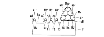
- each process will be sequentially described with reference to FIGS. 1 to 3D. 2A to 3D, for convenience of explanation, the unevenness formed on the particles M and the original plate S is extremely enlarged.
- the particle arranging step is performed by a method using a so-called LB method (Langmuir-Blodgett method). Specifically, it comprises a dropping step of dropping a dispersion liquid in which particles are dispersed in a solvent having a specific gravity smaller than that of water on the surface of the water in the water tank, and volatilizing the solvent from the dropped dispersion liquid.
- the particle arranging step is performed by a method having a single particle film forming step for forming a single particle film and a transfer step for transferring the single particle film to an original plate. This method combines the accuracy of monolayering, the ease of operation, the response to large areas, and reproducibility.
- the dispersion liquid is prepared by adding particles M in a solvent having a specific gravity smaller than that of water.
- a water tank trough
- water for developing the particles M on the liquid surface hereinafter sometimes referred to as lower layer water
- the particle M preferably has a hydrophobic surface. Further, it is preferable to select a hydrophobic solvent. By combining the hydrophobic particles M and the solvent with the lower layer water, as will be described later, self-organization of the particles M proceeds, and a two-dimensional close-packed single particle film is formed. It is also important that the solvent has high volatility.
- the volatile and hydrophobic solvent includes one or more volatile organic solvents such as chloroform, methanol, ethanol, isopropanol, acetone, methyl ethyl ketone, ethyl ethyl ketone, toluene, hexane, cyclohexane, ethyl acetate, and butyl acetate. Is mentioned.
- the surface thereof is usually hydrophilic, so that it is preferably used after being hydrophobized with a hydrophobizing agent.
- a hydrophobizing agent for example, a surfactant, a metal alkoxysilane, or the like can be used.
- Hydrophobization of the particles M can be performed by the same method using a surfactant, metal alkoxysilane, and the like similar to the hydrophobizing agent described in JP2009-162831A.
- the dispersion before dropping onto the liquid surface is microfiltered with a membrane filter or the like, and aggregated particles (from a plurality of primary particles) present in the dispersion are used. Secondary particles) are preferably removed. If the microfiltration is performed in advance as described above, it is difficult to generate a portion where two or more layers are formed or a defective portion where particles are not present, and it is easy to obtain a single particle film with high accuracy. If the formed single particle film has a defect portion having a size of several to several tens of ⁇ m, it is difficult to obtain a highly accurate single particle film.
- an LB trough device having a surface pressure sensor for measuring the surface pressure of the single particle film and a movable barrier for compressing the single particle film in the liquid surface direction was used in a transition process described in detail later.
- the dispersion liquid demonstrated above is dripped at the liquid level of lower layer water (drip process). Then, the solvent as the dispersion medium is volatilized, and the particles M are developed as a single layer on the liquid surface of the lower layer water to form a two-dimensional close packed single particle film (single particle film formation). Process).
- the particle concentration of the dispersion dropped into the lower layer water is preferably 1 to 10% by mass.
- the dropping rate is preferably 0.001 to 0.01 ml / second. If the concentration of the particles M in the dispersion and the amount of dripping are in such a range, the particles partially agglomerate in a cluster to form two or more layers, resulting in defective portions where no particles are present, and the pitch between the particles. The tendency to spread is suppressed. Therefore, it is easier to obtain a single particle film in which each particle is two-dimensionally closely packed with high accuracy.
- a single particle film is formed by self-organization of the particles M.
- the principle is that when the particles are aggregated, surface tension acts due to the dispersion medium existing between the particles.
- the particles M do not exist at random, but have a two-dimensional close packed structure. It forms automatically.
- the close-packing by surface tension can be said to be arrangement by lateral capillary force.
- three particles M having a spherical shape and high particle size uniformity, such as colloidal silica are brought together in contact with each other while floating on the water surface, the total length of the water line of the particle group is minimized. Surface tension acts. Therefore, as shown in FIG. 1, the three particles M are stabilized in an arrangement based on an equilateral triangle indicated by T in the figure.
- the single particle film forming step is preferably performed under ultrasonic irradiation conditions.
- the solvent of the dispersion liquid is volatilized while irradiating ultrasonic waves from the lower layer water to the water surface, the closest packing of particles M is promoted, and each particle M is more densely packed in two dimensions with a single particle film. Is obtained.
- the output of the ultrasonic wave is preferably 1 to 1200 W, and more preferably 50 to 600 W.
- the frequency of the ultrasonic wave is not particularly limited, but is preferably, for example, 28 kHz to 5 MHz, and more preferably 700 kHz to 2 MHz.
- the frequency is too high, energy absorption of water molecules begins, and a phenomenon in which water vapor or water droplets rise from the water surface is not preferable.
- the frequency is too low, the cavitation radius in the lower layer water becomes large, bubbles are generated in the water, and rise toward the water surface. If such bubbles accumulate under the single particle film, the flatness of the water surface is lost, which is inconvenient.
- a standing wave is generated on the water surface by ultrasonic irradiation. If the output is too high at any frequency, or if the wave height of the water surface becomes too high due to the tuning conditions of the ultrasonic transducer and the transmitter, the single particle film will be destroyed by the water surface wave, so care must be taken.
- the ultrasonic frequency and output are appropriately set in consideration of the above, close-packing of particles can be effectively promoted without destroying the single particle film being formed.
- the natural frequency calculated from the particle size of the particles should be used as a guide.
- the particle diameter is small, for example, 100 nm or less, the natural frequency becomes very high, and it is difficult to apply ultrasonic vibration as calculated.
- the necessary frequency can be reduced to a practical range.
- the ultrasonic irradiation time may be sufficient to complete the rearrangement of particles, and the required time varies depending on the particle size, ultrasonic frequency, water temperature, and the like.
- the normal production conditions are preferably 10 seconds to 60 minutes, more preferably 3 minutes to 30 minutes.
- the advantage obtained by ultrasonic irradiation is the effect of destroying the soft agglomerates of particles that are likely to occur when preparing a dispersion of nanoparticles, in addition to the closest packing of particles (to make the random array 6-way closest) The generated point defects, line defects, crystal transitions and the like are also repaired to some extent.
- the single particle film formed on the liquid surface by the single particle film forming step is transferred to the original plate S in a single layer state (transfer step).
- transfer step There is no particular limitation on the specific method of transferring the single particle film to the original plate S.
- the hydrophobic original plate S is lowered from above and brought into contact with the single particle film.
- a method of transferring the particle film to the original plate S and transferring it can be adopted.
- the original plate S in a substantially horizontal direction in the lower layer water of the water tank in advance before forming the single particle film, and gradually lowering the liquid level after forming the single particle film on the liquid surface, A method of transferring the single particle film to the original plate S can also be adopted. According to these methods, the single particle film can be transferred to the original plate S without using a special apparatus. However, it is preferable to adopt a so-called LB trough method in the transition process (see Journal of Materials and Chemistry, Vol. 11, 3333 (2001), Journal of Materials and Chemistry, Vol. 12, 3268 (2002)). ).
- a single particle film can be transferred to the original plate S without using a special apparatus, but also a secondary close-packing of a single particle film of a larger area. It is easy to transfer to the original plate S while maintaining the state.
- FIG. 2A and 2B schematically show an outline of the LB trough method.
- the particle M is extremely enlarged for convenience of explanation.
- the original plate S is preliminarily immersed in the lower layer water W in the water tank V, and the above-described dropping step and single particle film forming step are performed in this state to form the single particle film F ( FIG. 2A).
- the single particle film F can be transferred to the original plate S by pulling the original plate S upward while maintaining the substantially vertical direction (FIG. 2B).
- the single particle film F is the original plate S. It may be transferred only to the flat surface X.
- the single particle film F is formed only on the flat surface X while preventing the particles M from wrapping around from the flat surface X side to the back surface. Transfer is preferable because the single particle film F can be transferred more precisely. However, it can be transferred to both sides.
- the temperature condition of the transition step (temperature of the lower layer water), the pulling speed of the original plate S, etc. Even if it fluctuates somewhat, there is no fear that the single particle film F collapses and becomes multi-layered in the transfer step.
- the temperature of the lower layer water is usually about 10 to 30 ° C. depending on the environmental temperature which varies depending on the season and weather.
- a surface pressure sensor based on an unillustrated Wilhelmy plate or the like that measures the surface pressure of the single particle film F, and an illustration that compresses the single particle film F in the direction along the liquid surface. It is preferred to use an LB trough device with an approximate movable barrier. Thereby, the single particle film F having a larger area can be transferred to the original plate S more stably. According to such an apparatus, the single particle film F can be compressed to a preferable diffusion pressure (density) while measuring the surface pressure of the single particle film F, and is moved toward the original plate S at a constant speed. be able to.
- a preferable diffusion pressure is 5 to 80 mNm ⁇ 1 , more preferably 10 to 40 mNm ⁇ 1 . With such a diffusion pressure, it is easy to obtain a single particle film F in which each particle is two-dimensionally closely packed with higher accuracy.
- the speed at which the original sheet S is pulled up is preferably 0.5 to 20 mm / min.
- the temperature of the lower layer water is usually 10 to 30 ° C. as described above. Note that the LB trough device can be obtained as a commercial product.
- the single particle film F of the particles M can be transferred to the original plate S by the transfer step, but a fixing step for fixing the transferred single particle film F to the original plate S may be performed after the transfer step.
- a fixing step for fixing the transferred single particle film F to the original plate S may be performed after the transfer step.
- a method using a binder and a sintering method there are a method using a binder and a sintering method.
- a binder solution is supplied to the flat surface X side of the original plate S on which the single particle film is formed, and this is infiltrated between the particles M constituting the single particle film and the original plate S.
- the amount of the binder used is preferably 0.001 to 0.02 times the mass of the single particle film. If it is such a range, there will be too much binder and a binder will be clogged between particle
- the excess of the binder solution may be removed by using a spin coater or tilting the original plate S.
- the binder metal alkoxysilanes, general organic binders, inorganic binders and the like exemplified above as the hydrophobizing agent can be used.
- heat treatment may be appropriately performed depending on the type of the binder. .
- the original plate S on which the single particle film is formed may be heated to fuse each particle M constituting the single particle film to the original plate S.
- the heating temperature may be determined according to the material of the particle M and the material of the original plate S. However, since the particle M having a particle size of 1 ⁇ m ⁇ or less starts an interfacial reaction at a temperature lower than the original melting point of the material, the heating temperature is relatively low. Sintering is complete on the side. If the heating temperature is too high, the fusion area of the particles increases, and as a result, the shape of the single particle film may change, which may affect the accuracy. In addition, if heating is performed in air, the original plate S and each particle M may be oxidized.
- the original plate S may be sapphire, SiC, Si, MgAl 2 O 4 , LiTaO 3 , ZrB 2 , CrB 2 or the like.
- plate material which consists of these materials can be used.
- sapphire is preferable in terms of mechanical stability, thermal stability, optical stability, and chemical stability.
- the base plate S provided with a concavo-convex structure is used as a substrate of a bottom emission type organic light emitting diode as it is, a transparent body that transmits visible light is used as the base plate S so that light can be extracted from the substrate.
- the original plate S one having a transmittance of 70% or more, preferably 80% or more, and more preferably 90% or more without giving a bias to the spectrum in the visible light range (wavelength 380 nm to 800 nm).
- the material of the original plate S that is a transparent body may be an inorganic material, an organic material, or a combination thereof.
- the inorganic material examples include various glasses such as quartz glass, alkali-free glass, white plate glass, and transparent inorganic minerals such as mica.
- the organic material examples include a resin film such as a cycloolefin film and a polyester film, and a fiber reinforced plastic material in which fine fibers such as cellulose nanofiber are mixed in the resin film.
- the original plate S When a substrate provided with a concavo-convex structure on the original plate S is used as it is as a substrate of a top emission type organic light emitting diode, the original plate S does not necessarily have to be transparent because light is extracted from the side opposite to the substrate. Therefore, the same material as that for the substrate of the bottom emission type organic light emitting diode can be used, and for example, a metal plate such as a stainless plate or a copper plate, a silicon wafer, or the like can be used.
- a metal plate such as a stainless plate or a copper plate, a silicon wafer, or the like is used. Can do.
- particles M examples include inorganic particles such as metals and metal oxides, and organic polymers such as polystyrene and polymethyl methacrylate. These may be used alone or in combination of two or more. By selecting the material of the particles M and the dry etching conditions described later, the height and shape of the concavo-convex structure to be formed can be adjusted.
- the particles M are preferably inorganic particles.
- the inorganic particles for example, particles composed of oxides, nitrides, carbides, borides, sulfides, selenides, metals and the like, metal particles, and the like can be used.
- oxides examples include silica, alumina, zirconia, titania, ceria, zinc oxide, tin oxide, and yttrium aluminum garnet (YAG). Further, these constituent elements are partially substituted with other elements. Can also be used.
- nitride examples include silicon nitride, aluminum nitride, boron nitride, and the like, and those obtained by partially replacing these constituent elements with other elements can also be used.
- a compound such as sialon composed of silicon, aluminum, oxygen, and nitrogen can also be used.
- carbide examples include SiC, boron carbide, diamond, graphite, fullerenes, and those in which these constituent elements are partially substituted with other elements can also be used.
- Examples of the boride that can be used include ZrB 2 , CrB 2, and the like, and those obtained by partially substituting these constituent elements with other elements can also be used.
- Examples of the sulfide that can be used include zinc sulfide, calcium sulfide, cadmium sulfide, strontium sulfide, and the like, and those obtained by partially replacing these constituent elements with other elements can also be used.
- Examples of the selenide that can be used include zinc selenide, cadmium selenide, and the like, and those obtained by partially substituting these constituent elements with other elements can also be used.
- As the metal that can be used particles made of one or more metals selected from the group consisting of Si, Ni, W, Ta, Cr, Ti, Mg, Ca, Al, Au, Ag, and Zn are used. Can do.
- Each of the inorganic particles can be used alone as the particle M, or a mixture of these inorganic particles can be used as the particle M.
- coated particles such as inorganic particles made of nitride coated with an oxide can be used as the particles M.
- phosphor particles obtained by introducing an activator such as cerium or europium into the inorganic particles can be used as the particles M.
- oxides are preferable in terms of shape stability, and silica is more preferable among them.
- a plurality of particles M are arranged in a substantially single layer on the flat surface X which is one surface of the original plate S by the particle arranging step. That is, the single particle film F of the particles M is formed on the flat surface X.
- the particle arranging step it is preferable to arrange a plurality of particles M on the original plate S in a single layer so that the deviation D (%) of the arrangement defined by the following formula (1) is 15% or less.
- D [%]
- A is the average particle diameter of the particle
- B is the most frequent pitch between the particle
- the deviation D is preferably 10% or less, and more preferably 1.0 to 3.0%.
- the average particle size A of the particles M is the average primary particle size of the particles M constituting the single particle film, and the particle size distribution obtained by the particle dynamic light scattering method is fitted to a Gaussian curve. It can obtain
- the pitch between the particles M is the distance between the vertices of two adjacent particles M in the sheet surface direction, and the most frequent pitch B is an average of these. If the particles M are spherical, the distance between the vertices of the adjacent particles M is equal to the distance between the centers of the adjacent particles M.
- the most frequent pitch B between the particles M is obtained as follows. First, an atomic force microscope image of a randomly selected region in a single particle film with a side parallel to the sheet surface 30 to 40 times the predicted mode pitch B between the particles M is obtained. obtain. For example, in the case of a single particle film using particles M having a particle size of 300 nm, an image of a region of 9 ⁇ m ⁇ 9 ⁇ m to 12 ⁇ m ⁇ 12 ⁇ m is obtained. Then, this image is waveform-separated by Fourier transform to obtain an FFT image (fast Fourier transform image). Next, the distance from the zero-order peak to the primary peak in the profile of the FFT image is obtained.
- FFT image fast Fourier transform image
- the reciprocal of the distance thus obtained is the most frequent pitch B 1 in this region.
- Such processing is similarly performed for a total of 25 or more regions having the same area selected at random, and the most frequent pitches B 1 to B 25 in each region are obtained.
- the average value of the most frequent pitches B 1 to B 25 in the 25 or more regions thus obtained is the most frequent pitch B in the equation (1).
- the regions are preferably selected at least 1 mm apart, more preferably 5 mm to 1 cm apart.
- the variation in pitch between the particles M in each image can be evaluated from the area of the primary peak in the profile of the FFT image.
- This misalignment D is an index indicating the degree of closest packing of the particles M. That is, a small deviation D of the arrangement of particles means that the degree of close-packing is high, the interval between the particles is controlled, and the accuracy of the arrangement is high.
- the coefficient of variation of the particle size of the particles M is preferably 20% or less, and preferably 10% or less. More preferably, it is 5% or less.
- the pitch of the concavo-convex structure provided on the original plate S according to the present invention is equivalent to the most frequent pitch B between the particles M.
- the pitch of the concavo-convex structure is substantially equal to the average particle diameter A of the particles M. Therefore, by appropriately selecting the average particle diameter A of the particles M, a desired pitch can be obtained.
- the uneven structure can be formed with high accuracy.
- the particles M can be easily arranged so that the deviation D is 15% or less by the particle arranging step of the present invention. That is, an etching mask in which particles M are closely packed with a single layer can be arranged on the original plate S with very high accuracy.
- a portion where the particle M does not cover the original plate S and a portion where the particle M overlaps are generated only slightly by the particle arranging step of the present invention.
- the frequency per unit area of the portion where the particles overlap is 1 to 1000 locations / mm 2 .
- the case where the particles are overlapped to this extent is called a substantially single layer.
- FIG. 3A is a diagram showing a state of a portion where such a slight defect occurs after the particle arranging step. That is, in FIG. 3A, particles M1 to M10 (a plurality of particles M) are arranged on the flat surface X of the original plate S. The arrangement of the particles M1 to M10 is defective at the following two points. a. There is a portion where the flat surface X is not covered with the particles M between the particles M1 and the particles M2. b. The particles M8 to M10 are superposed on the particles M5 to M7.
- FIG. 3B shows changes in the particles M and the original plate S when this dry etching process is performed in the following two stages (S1) and (S2). If the flat surfaces f1 to fn described in FIG. 5 are not necessary, the step (S1) is not necessary.
- S1 A step of dry etching the particles M under the condition that the particles M are etched and the original plate S is not substantially etched.
- S2 A step of dry-etching the original plate S using the particles remaining in (S1) as an etching mask under conditions where both the particles M and the original plate S are substantially etched.
- an etching gas may be appropriately selected.
- the original plate S is sapphire and the particle M is silica
- one or more selected from CF 4 , SF 6 , CHF 3 , C 2 F 6 , C 3 F 8 , CH 2 F 2 , and NF 3 Dry etching is preferably performed using this gas.
- the particles M can be etched with little influence on the original plate S.
- the etching step (S1) needs to be performed so that particles functioning as an etching mask remain in the etching step (S2).
- the size of the particle M in the surface direction (horizontal direction) of the original plate S (hereinafter referred to as the “height”) is maintained while maintaining a sufficient diameter (hereinafter referred to as “height”) of the particles M in the thickness direction (vertical direction) of the original plate S.
- the bias power may be set low or the pressure may be reduced.
- the etching step (S2) is preferably performed under the condition that the dry etching selectivity of the above formula (2) is greater than 100%, more preferably 200% or more, and even more preferably 300% or more.
- an etching gas may be appropriately selected according to the material of the original plate S and the particles M.
- the original plate S is quartz and the particles M are colloidal silica
- Ar, CF 4 or the like can be used.
- dry etching may be performed using one or more gases selected from Cl 2 , BCl 3 , SiCl 4 , HBr, HI, and HCl.
- a reactive ion etching apparatus As an etching apparatus that can be used in the etching steps (S1) and (S2), a reactive ion etching apparatus, an ion beam etching apparatus, or the like, which can perform anisotropic etching, has a minimum bias electric field of about 20 W. As long as it can generate. There are no particular restrictions on the specifications such as the plasma generation method, electrode structure, chamber structure, and frequency of the high-frequency power source.
- the particles M arranged in a single layer such as the particles M2 to M4, are etched to become small, and a gap is generated therebetween.
- the particles M1 and M10 are also etched and reduced in the same manner as the particles M2 to M4.
- the particles M5 to M9 are masked by the particles superposed on the upper side, the degree of etching is limited.
- the original plate S is dry-etched using the particles remaining in the step (S1) as an etching mask.
- Etching of the flat surface X proceeds while maintaining a substantially flat surface in a gap portion formed by etching and reducing the particles M arranged in a single layer, such as the particles M2 to M4. Further, on the lower flat surface X of the remaining particles M1 to M4, as each particle M is gradually etched to become smaller, it gradually goes from the lower portion around each particle M toward the lower portion in the center. Since the etching progresses, the etching surface becomes inclined. On the other hand, the particles M1 are further etched, but the particles M5 to M9 are limited in the degree of etching because the upper overlapping particles serve as a mask. Under the particles M5 to M10, the etching of the flat surface X hardly proceeds.
- the etching process is terminated before the particles M1 to M4 arranged in a substantially single layer disappear.
- the particles M1 to M4 and M10 become particles M1 ′ to M4 ′ and M10 ′ having small particle diameters.
- the portions of the particles M5 to M9 that are masked by the overlapping particles remain, and become particles M5 ′ to M9 ′ as shown in FIG. 3B. Further, an etching residue Mx is deposited around each remaining particle.
- the etching process may be completed so that the volume of the particles M1 ′ to M4 ′ and M10 ′ at the end of the etching process is about 10 to 90% of the volume of the particles M1 to M4 and M10.
- the etching process may be terminated so that the mass ratio of the particles M1 ′ to M4 ′ and M10 ′ and the particles M1 to M4 and M10 at the end of the etching process is 1: 1.1 to 1: 100.
- the etching process may be terminated by setting conditions such that the step is completed with an etching time that provides a target uneven structure step, for example, a step of 10 nm to 200 nm.
- the uneven structure of the original plate S ′ is completed.
- frustoconical convex portions c1 to c4 having the top surfaces of the remaining particles M1 ′ to M4 ′ are formed.
- a convex portion c5 having a wide top surface is formed below the particles M5 to M10.
- the particles M are etched and reduced in the step (S1).
- the flat surfaces f1 to f3 are formed corresponding to the generated gap portions.
- a coarse flat surface fx is formed between the convex part c1 and the convex part c2. If the step (S1) is omitted, the flat surfaces f1 to f3 are not formed.
- the pitch of the concavo-convex structure formed on the original plate S ′ is equivalent to the most frequent pitch B between the particles M described above. Since the arrangement of the particles M in FIG. 3A has a high degree of fine packing, by appropriately selecting the average particle diameter A of the particles M, it is possible to accurately form an uneven structure with a desired pitch.
- the shape of the normally formed convex portions c1 to c4 is not limited to a strict truncated cone, but may be a bamboo shoot shape whose side surface bulges outward or a hemispherical convex portion cut by a plane parallel to the bottom surface. .
- the shape of the projections c1 to c4 can be adjusted by the bias power, the pressure in the vacuum chamber, and the type of etching gas. For example, if the pressure is lowered, the shape has a gentle inclination angle.
- the flat surfaces f1 to f3 are kept flat as the dry etching selectivity in the step (S1) is lower. It is preferable that the gap between the convex portions be a flat surface because the film forming property of a layer to be subsequently laminated on the substrate is improved.
- the remaining particles M are removed.
- the particles M can be removed by a chemical removal method using an etchant having an etching property with respect to the particles M and an etching resistance with respect to the original plate S ′, or a physical removal method using a brush roll cleaning machine or the like. Since the etching process is completed before the particles M arranged in a single layer disappear, the adhesion force of the etching residue Mx is not strong, and the etching residue Mx can also be removed by the above-described normal chemical removal method or physical removal method. . Thereby, an original plate S ′ having a concavo-convex structure shown in FIG. 3C is obtained.
- the original plate S ′ does not have a convex portion (spike) protruding from the apex, including the convex portion c5.
- Spikes are considered to cause defects in the layers stacked on the substrate, which in turn cause defects due to short circuits and problems of reduced life.
- the presence of the convex portion c5 having a wide top surface and the coarse flat surface fx does not cause a defect of a layer laminated on the substrate like a spike.
- the convex portion c5 and the coarse flat surface fx (lack of the convex portion) are factors that reduce the light extraction efficiency improvement effect, but are very slight from the viewpoint of the light extraction efficiency improvement effect obtained as a whole. It will not be a trap.
- the convex portions c1 to c5 are further digged into the slopes of the bottoms to become convex portions c1 ′ to c5 ′.
- 'flat surfaces f1 to f3 become further dug flat surfaces f1' to f3 '
- coarse flat surface fx becomes further dug deep flat surface fx'.
- the fixed object cx is strongly fixed on the convex part c5 ′. Therefore, it is difficult to remove the fixed substance cx at this stage by a normal chemical removal method or physical removal method. As a result, in the obtained original plate Sx, a spike in which the convex portion c5 ′ and the fixed object cx are superimposed is generated.
- the concavo-convex substrate of the present invention may be the original plate S itself after the removal step, or a concavo-convex substrate obtained by transferring the concavo-convex structure a plurality of times. That is, the manufacturing method of the concavo-convex substrate of the present invention may include a transfer step of transferring the concavo-convex structure provided on the original plate S after the removing step a plurality of times. By transferring a plurality of times, a concavo-convex substrate having a concavo-convex structure equivalent to the concavo-convex structure provided on the original plate S after the removing step is obtained.
- the transfer process By performing the transfer process, a plurality of concave and convex substrates can be efficiently manufactured.
- the concavo-convex structure of the original plate S after the removal process is transferred to a mold (mold or stamper) (first transfer), and then the concavo-convex structure of the mold is transferred (second transfer), and transferred twice. It is preferable that it is this process.
- an electroforming method as disclosed in, for example, Japanese Patent Application Laid-Open No. 2009-158478 is preferable.
- the method for transferring the concavo-convex structure of the mold include a nanoimprint method, a hot press method, an injection molding method, and a UV embossing method as disclosed in Japanese Patent Application Laid-Open No. 2009-158478.
- the nanoimprint method is suitable for transferring a fine uneven structure.
- the light-emitting diode (inorganic light-emitting diode) of the present invention includes the concavo-convex substrate of the present invention and a semiconductor functional layer laminated on the surface on which the concavo-convex structure of the concavo-convex substrate is formed.
- the semiconductor constituting the semiconductor functional layer is preferably a group III-V nitride semiconductor in which the group V element is nitrogen. This is because the group III-V nitride semiconductor needs to be formed on a substrate such as sapphire.
- the group III element is a group 13 element in IUPAC
- the group V element is a group 15 element in IUPAC.
- Typical group III-V nitride semiconductors are gallium nitride and indium nitride. Strictly speaking, aluminum nitride is an insulator, but in the present invention, it is treated as corresponding to a group III-V nitride semiconductor according to the practice of the light emitting diode field.
- the layer structure of the semiconductor functional layer is a structure necessary for the operation of the III-V nitride light emitting diode.
- the semiconductor functional layer has at least an n-type conductivity layer, a p-type conductivity layer, and a light emitting layer sandwiched therebetween, and is composed of a III-V group nitride semiconductor layer. Those are preferred.
- the III-V nitride semiconductor functional layer includes high-quality layers. It may include other layers necessary to make crystals.
- the other layer may be a single layer or a multilayer layer (including a thick film layer and a superlattice thin film layer).
- a buffer layer may be included as another layer.
- Each of the above layers may also be composed of a plurality of layers.
- Specific semiconductor functional layers include a buffer layer made of GaN, AlN, etc., an n-type conductive layer (clad layer) made of n-GaN, n-AlGaN, etc., a light emitting layer made of InGaN, GaN, etc.
- Examples include a multilayer film in which a p-type conductive layer (clad layer) made of undoped GaN, p-GaN, etc., and a cap layer made of Mg-doped AlGaN and Mg-doped GaN are sequentially stacked (for example, Japanese Patent Laid-Open No. Hei 6).
- electrodes made of a metal such as Ni, Au, Pt, Pd, Rh, Ti, and Al can be used as an n-type electrode and a p-type electrode for supplying current to the light emitting layer.
- electrodes made of a metal such as Ni, Au, Pt, Pd, Rh, Ti, and Al can be used as an n-type electrode and a p-type electrode for supplying current to the light emitting layer.
- the light-emitting diode (inorganic light-emitting diode) of the present invention has a semiconductor functional layer on a concavo-convex substrate on which a concavo-convex structure having a desired pitch is accurately formed. Therefore, sufficient light extraction efficiency can be obtained.
- the semiconductor functional layer is laminated on an uneven substrate without spikes, defects are unlikely to occur. As a result, the occurrence of defects due to short circuits and the problem of life reduction are improved.
- the method for producing a light emitting diode (inorganic light emitting diode) of the present invention comprises a step of obtaining a concavo-convex substrate by the method for producing a concavo-convex substrate of the present invention, and at least a light emitting layer on the surface on which the concavo-convex structure of the obtained concavo-convex substrate is formed.
- a laminating step of laminating a semiconductor functional layer comprises a step of obtaining a concavo-convex substrate by the method for producing a concavo-convex substrate of the present invention, and at least a light emitting layer on the surface on which the concavo-convex structure of the obtained concavo-convex substrate is formed.
- a known epitaxial growth method such as MOVPE method (metal organic vapor phase epitaxy), MBE method (molecular beam epitaxy method), HVPE method (hydride vapor phase epitaxy) can be used.
- MOVPE method metal organic vapor phase epitaxy
- MBE method molecular beam epitaxy method
- HVPE method hydrogen vapor phase epitaxy
- Group III materials include general formulas such as trimethylgallium [(CH 3 ) 3 Ga, hereinafter sometimes referred to as TMG] and triethylgallium [(C 2 H 5 ) 3 Ga, hereinafter sometimes referred to as TEG].
- Trialkylgallium represented by R 1 R 2 R 3 Ga (where R 1 , R 2 and R 3 represent lower alkyl groups), trimethylaluminum [(CH 3 ) 3 Al, hereinafter referred to as TMA
- R 1 R 2 R 3 such as triethylaluminum [(C 2 H 5 ) 3 Al, hereinafter sometimes referred to as TEA], triisobutylaluminum [(i-C 4 H 9 ) 3 Al]
- Trialkylaluminum represented by Al (wherein R 1 , R 2 and R 3 represent lower alkyl groups), trimethylamine alane [(CH 3 ) 3 N: AlH 3 ], trimethylindium [(CH 3 ) 3 In, hereinafter sometimes referred to as TMI], and general formulas R 1 R 2 R 3 In (where R 1 , R 2 , R 3 are such as triethylindium [(C 2 H 5 ) 3 In])
- Group V raw material examples include ammonia, hydrazine, methyl hydrazine, 1,1-dimethylhydrazine, 1,2-dimethylhydrazine, t-butylamine, and ethylenediamine. These can be used alone or in any combination. Among these raw materials, ammonia and hydrazine are preferable because they do not contain carbon atoms in their molecules and thus cause less carbon contamination in the semiconductor.
- gases such as nitrogen, hydrogen, argon, and helium can be used singly or as a mixture, and hydrogen and helium are preferred as the growth atmosphere gas and the carrier gas of the organometallic raw material.
- the semiconductor functional layer is laminated on the concavo-convex substrate on which the concavo-convex structure having a desired pitch is accurately formed. Therefore, a light-emitting diode that can obtain sufficient light extraction efficiency can be obtained.
- the semiconductor functional layer is stacked on the uneven substrate without spikes, it is possible to obtain a light emitting diode in which defects in the semiconductor functional layer are less likely to be generated, and as a result, the occurrence of defects due to short circuits and the problem of life reduction are improved.
- the light-emitting diode (organic light-emitting diode) according to the present invention includes a concavo-convex substrate according to the present invention, an anode conductive layer provided on a surface on which the concavo-convex structure is formed, and an organic electroluminescence layer (hereinafter referred to as “organic EL”). And a laminated structure including a cathode conductive layer.
- the specific laminated structure various known laminated structures can be adopted.
- the bottom emission type it is a laminated structure having an anode conductive layer, an organic EL layer, and a cathode conductive layer that are sequentially laminated on a transparent uneven substrate.
- the top emission type of the anode top it is a laminated structure having a cathode conductive layer, an organic EL layer, and an anode conductive layer, which are sequentially laminated on an uneven substrate.
- the top emission type of the cathode top is a laminated structure having a reflective film, an anode conductive layer, an organic EL layer, and a cathode conductive layer, which are sequentially laminated on an uneven substrate.
- the organic EL layer is a layer including at least a light emitting layer containing an organic light emitting material and may be composed of only the light emitting layer, but generally includes other layers other than the light emitting layer.
- the other layer may be composed of an organic material or an inorganic material as long as the function of the light emitting layer is not impaired.
- it can be composed of five layers including a hole injection layer, a hole transport layer, a light emitting layer, an electron transport layer, and an electron injection layer from the side close to the anode conductive layer.
- the most important of these layers is a light emitting layer.
- the hole injection layer and the electron injection layer can be omitted depending on the layer structure.
- the electron transport layer can also serve as a light emitting layer.
- the material which comprises these layers is not specifically limited, A well-known thing can be used.
- An organic light emitting material is used as a material constituting the light emitting layer.
- the organic light-emitting material include Tris [1-phenylisoquinoline-C2, N] iridium (III) (Ir (piq) 3 ), 1,4-bis [4- (N, N-diphenylaminostyrene) (DPAVB), Bis [2- (2-benzoxazolyl) phenolato] Zinc (II) (ZnPBO) and other dye compounds can be mentioned.
- the host material include a hole transport material and an electron transport material.
- organic materials constituting the hole injection layer, the hole transport layer, and the electron transport layer organic materials are generally used.
- Examples of the material constituting the hole injection layer include compounds such as 4,4 ′, 4 ′′ -tris (N, N-2-naphthylphenylamino) triphenylamine (2-TNATA).
- aromatic amine compounds such as diamine (NPD), copper phthalocyanine (CuPc), N, N′-Diphenyl-N, N′-di (m-tolyl) benzidine (TPD), and the like.
- Examples of the material (electron transport material) constituting the electron transport layer include 2,5-Bis (1-naphthyl) -1,3,4-oxadiazole (BND), 2- (4-tert-Butylphenyl) -5.
- Examples thereof include oxadiazole compounds such as-(4-biphenyl) -1,3,4-oxadiazole (PBD), and metal complex compounds such as Tris (8-quinolinolato) aluminum (Alq).
- As a material constituting the electron injection layer lithium fluoride (LiF) or the like can be used.
- the total thickness of the organic EL layer is usually 30 to 500 nm.
- the thickness of each layer which comprises an organic light emitting diode can be measured with a spectroscopic ellipsometer, a contact-type level difference meter, AFM, etc.
- anode conductive layer In the case of the bottom emission type or the top emission type of the anode top, a transparent conductor that transmits visible light is used for the anode conductive layer.
- the material of the transparent conductor constituting the anode conductive layer include indium tin oxide (Indium Tin Oxide (ITO)), indium zinc oxide (Indium Zinc Oxide (IZO)), and zinc oxide (Zinc Oxide (ZnO)). )), Zinc-tin oxide (Zinc Tin Oxide (ZTO)) and the like.
- the anode conductive layer In the case of the top emission type of the cathode top, the anode conductive layer is not required to have visible light transmittance.
- a material for the anode conductive layer for example, aluminum, silver, or an alloy mainly composed of them can be used in addition to the transparent conductor.
- the thickness of the anode conductive layer is usually 50 to 500 nm.
- Cathode conductive layer Examples of the material for the cathode conductive layer include Ag, Al, or an alloy of Ag and Al. A very small amount of a lithium compound such as LiF may be interposed between the organic EL layer.
- the thickness of the cathode conductive layer is usually 50 to 3000 nm.
- the light-emitting diode (organic light-emitting diode) of the present invention has a laminated structure including an anode conductive layer, an organic electroluminescence layer, and a cathode conductive layer on a concavo-convex substrate on which a concavo-convex structure with a desired pitch is accurately formed. Therefore, sufficient light extraction efficiency can be obtained.
- the laminated structure is laminated on an uneven substrate without spikes, defects are unlikely to occur. As a result, the occurrence of defects due to short circuits and the problem of life reduction are improved.
- the method for producing a light-emitting diode (organic light-emitting diode) according to the present invention comprises a step of obtaining a concavo-convex substrate by the method for producing a concavo-convex substrate of the present invention, and an anode conductive layer on the surface on which the concavo-convex structure of the obtained concavo-convex substrate is formed. And a lamination process for forming a laminated structure including the organic EL layer and the cathode conductive layer.
- the method for laminating each of the above layers is not particularly limited, and a known method used in the production of a general organic light emitting diode can be used.
- the anode conductive layer and the cathode conductive layer can be formed by a sputtering method, a vacuum deposition method, or the like, respectively.
- the hole injection layer, hole transport layer, light emitting layer, electron transport layer, and electron injection layer are formed by a vacuum deposition method. Since these layers are very thin, the concavo-convex structure on the concavo-convex substrate surface is reflected on each layer including the cathode conductive layer by sequentially laminating the layers.
- the cathode conductive layer has an uneven structure, surface plasmons are converted into propagating light on the surface of the cathode conductive layer.
- a laminated structure including an anode conductive layer, an organic electroluminescence layer, and a cathode conductive layer is formed on a concavo-convex substrate on which a concavo-convex structure having a desired pitch is accurately formed. Therefore, a light-emitting diode that can obtain sufficient light extraction efficiency can be obtained.
- the multilayer structure is formed on the uneven substrate without spikes, it is possible to obtain a light-emitting diode in which defects in each layer of the multilayer structure are less likely to occur, and as a result, the occurrence of defects due to short circuits and the problem of life reduction are improved.
- the organic light emitting diode of the present invention at the interface of all layers of the anode conductive layer, the organic EL layer, the cathode conductive layer, and an intermediate layer appropriately provided between these layers, or at the interface of any one or more layers
- the concavo-convex structure reflecting the concavo-convex structure on the concavo-convex substrate of the present invention is preferably formed.
- the organic thin-film solar cell of the present invention is provided with a concavo-convex substrate obtained by the production method of the present invention.
- a known layer structure can be adopted as the layer structure formed on the uneven substrate. For example, a structure in which an anode, a hole injection layer, a hole transport layer, an electron donating organic semiconductor layer, an electron accepting organic semiconductor layer, an electron transport layer, and a cathode are sequentially laminated on the surface of the uneven substrate on which the uneven structure is formed. be able to.
- a method for laminating each layer a known method can be adopted.
- a concavo-convex structure reflecting the concavo-convex structure on the concavo-convex substrate of the present invention is formed at the interface of one or more layers.
- a concavo-convex substrate for obtaining a photoelectric device such as an organic or inorganic light-emitting diode with improved light extraction efficiency without causing defects due to a short circuit and a problem of life reduction.
- a concavo-convex substrate organic or inorganic light-emitting diodes and organic thin-film solar cells with improved light extraction efficiency or light utilization efficiency can be produced without causing defects due to short circuits and problems of reducing the lifetime.
Abstract
L'invention porte sur un procédé pour fabriquer ce substrat non uniforme, qui comprend : une étape d'agencement de particules pour agencer une pluralité de particules (M, M1 à M6) sur une feuille d'origine (S) ; une étape de gravure d'utilisation des particules (M) en tant que masque de gravure pour réaliser une gravure sèche de la feuille d'origine (S) et former une structure non uniforme sur une surface de la feuille d'origine (S) ; et une étape de retrait pour retirer les particules (M) restant sur la structure non uniforme formée.
Applications Claiming Priority (4)
| Application Number | Priority Date | Filing Date | Title |
|---|---|---|---|
| JP2013-023864 | 2013-02-08 | ||
| JP2013023864 | 2013-02-08 | ||
| JP2013-267926 | 2013-12-25 | ||
| JP2013267926A JP2014170920A (ja) | 2013-02-08 | 2013-12-25 | 凹凸基板及び発光ダイオードの製造方法、並びに凹凸基板、発光ダイオード及び有機薄膜太陽電池 |
Publications (1)
| Publication Number | Publication Date |
|---|---|
| WO2014123193A1 true WO2014123193A1 (fr) | 2014-08-14 |
Family
ID=51299784
Family Applications (1)
| Application Number | Title | Priority Date | Filing Date |
|---|---|---|---|
| PCT/JP2014/052781 WO2014123193A1 (fr) | 2013-02-08 | 2014-02-06 | Procédé pour fabriquer un substrat non uniforme et une diode électroluminescente, substrat non uniforme, diode électroluminescente, et cellule solaire en couches minces organique |
Country Status (3)
| Country | Link |
|---|---|
| JP (1) | JP2014170920A (fr) |
| TW (1) | TW201442278A (fr) |
| WO (1) | WO2014123193A1 (fr) |
Cited By (1)
| Publication number | Priority date | Publication date | Assignee | Title |
|---|---|---|---|---|
| JPWO2016063915A1 (ja) * | 2014-10-24 | 2017-08-03 | 王子ホールディングス株式会社 | 光学素子、光学複合素子及び保護フィルム付光学複合素子 |
Families Citing this family (4)
| Publication number | Priority date | Publication date | Assignee | Title |
|---|---|---|---|---|
| EP3016157A4 (fr) * | 2013-06-27 | 2017-03-29 | Oji Holdings Corporation | Cellule solaire organique à couches minces et son procédé de fabrication |
| JP6638245B2 (ja) * | 2014-12-12 | 2020-01-29 | 王子ホールディングス株式会社 | 半導体発光素子用基板、および、半導体発光素子 |
| TWI692896B (zh) * | 2015-09-10 | 2020-05-01 | 日商王子控股股份有限公司 | 有機發光二極體之製造方法及有機發光二極體 |
| JP6561706B2 (ja) * | 2015-09-10 | 2019-08-21 | 王子ホールディングス株式会社 | 金型、有機発光ダイオードの製造方法及び有機発光ダイオード |
Citations (4)
| Publication number | Priority date | Publication date | Assignee | Title |
|---|---|---|---|---|
| JP2006190573A (ja) * | 2005-01-06 | 2006-07-20 | Toshiba Corp | 有機エレクトロルミネッセンス素子およびその製造方法 |
| JP2007019318A (ja) * | 2005-07-08 | 2007-01-25 | Sumitomo Chemical Co Ltd | 半導体発光素子、半導体発光素子用基板の製造方法及び半導体発光素子の製造方法 |
| WO2008001670A1 (fr) * | 2006-06-30 | 2008-01-03 | Oji Paper Co., Ltd. | Masque de gravure de film monoparticulaire et son procédé de production, procédé de production d'une structure fine avec un masque de gravure de film monoparticulaire et structure fine obtenue à l'aide du procédé de production |
| JP2009158478A (ja) * | 2007-12-07 | 2009-07-16 | Oji Paper Co Ltd | プラズモニック結晶面発光体、画像表示装置及び照明装置 |
-
2013
- 2013-12-25 JP JP2013267926A patent/JP2014170920A/ja active Pending
-
2014
- 2014-02-06 WO PCT/JP2014/052781 patent/WO2014123193A1/fr active Application Filing
- 2014-02-07 TW TW103104144A patent/TW201442278A/zh unknown
Patent Citations (4)
| Publication number | Priority date | Publication date | Assignee | Title |
|---|---|---|---|---|
| JP2006190573A (ja) * | 2005-01-06 | 2006-07-20 | Toshiba Corp | 有機エレクトロルミネッセンス素子およびその製造方法 |
| JP2007019318A (ja) * | 2005-07-08 | 2007-01-25 | Sumitomo Chemical Co Ltd | 半導体発光素子、半導体発光素子用基板の製造方法及び半導体発光素子の製造方法 |
| WO2008001670A1 (fr) * | 2006-06-30 | 2008-01-03 | Oji Paper Co., Ltd. | Masque de gravure de film monoparticulaire et son procédé de production, procédé de production d'une structure fine avec un masque de gravure de film monoparticulaire et structure fine obtenue à l'aide du procédé de production |
| JP2009158478A (ja) * | 2007-12-07 | 2009-07-16 | Oji Paper Co Ltd | プラズモニック結晶面発光体、画像表示装置及び照明装置 |
Cited By (5)
| Publication number | Priority date | Publication date | Assignee | Title |
|---|---|---|---|---|
| JPWO2016063915A1 (ja) * | 2014-10-24 | 2017-08-03 | 王子ホールディングス株式会社 | 光学素子、光学複合素子及び保護フィルム付光学複合素子 |
| CN107076877A (zh) * | 2014-10-24 | 2017-08-18 | 王子控股株式会社 | 光学元件、光学复合元件及附保护膜的光学复合元件 |
| EP3211458A4 (fr) * | 2014-10-24 | 2018-06-06 | Oji Holdings Corporation | Élément optique, élément composite optique et élément composite optique comportant un film protecteur attaché |
| TWI657927B (zh) * | 2014-10-24 | 2019-05-01 | 日商王子控股股份有限公司 | 光學元件、光學複合元件及附保護膜之光學複合元件 |
| US10444407B2 (en) | 2014-10-24 | 2019-10-15 | Oji Holdings Corporation | Optical element including a plurality of concavities |
Also Published As
| Publication number | Publication date |
|---|---|
| TW201442278A (zh) | 2014-11-01 |
| JP2014170920A (ja) | 2014-09-18 |
Similar Documents
| Publication | Publication Date | Title |
|---|---|---|
| JP6036830B2 (ja) | 半導体発光素子用基板及び半導体発光素子、並びにこれらの製造方法 | |
| US8420439B2 (en) | Method of producing a radiation-emitting thin film component and radiation-emitting thin film component | |
| JP5944489B2 (ja) | 半導体薄膜構造及びその形成方法 | |
| JP2007019318A (ja) | 半導体発光素子、半導体発光素子用基板の製造方法及び半導体発光素子の製造方法 | |
| JP5539395B2 (ja) | 半導体素子、発光素子及びこれの製造方法 | |
| TWI419354B (zh) | Iii族氮化物半導體發光元件及其製造方法 | |
| WO2014123193A1 (fr) | Procédé pour fabriquer un substrat non uniforme et une diode électroluminescente, substrat non uniforme, diode électroluminescente, et cellule solaire en couches minces organique | |
| TW201507201A (zh) | Led用圖案晶圓、led用磊晶晶圓及led用磊晶晶圓之製造方法 | |
| US8404504B1 (en) | Method for making light emitting diode | |
| Polyakov et al. | III‐Nitride Nanowires as Building Blocks for Advanced Light Emitting Diodes | |
| US20130143341A1 (en) | Method for making light emitting diode | |
| JP6206336B2 (ja) | 半導体発光素子用基板、半導体発光素子、半導体発光素子用基板の製造方法、および、半導体発光素子の製造方法 | |
| TW202015273A (zh) | 有機發光二極體製造用之模具 | |
| KR20130120110A (ko) | 발광다이오드 및 그 제조방법 | |
| KR101154321B1 (ko) | 발광다이오드 및 그 제조방법 | |
| CN102005514A (zh) | 采用纳米压印技术的ⅲ族氮化物半导体发光装置 | |
| JP5957142B2 (ja) | 半導体発光素子の製造方法、および半導体発光素子 | |
| JP2019125649A (ja) | 半導体発光素子用基材及び半導体発光素子 | |
| Chiu et al. | Efficiency enhancement of GaN-based LED using nanotechnology |
Legal Events
| Date | Code | Title | Description |
|---|---|---|---|
| 121 | Ep: the epo has been informed by wipo that ep was designated in this application |
Ref document number: 14748654 Country of ref document: EP Kind code of ref document: A1 |
|
| NENP | Non-entry into the national phase |
Ref country code: DE |
|
| 122 | Ep: pct application non-entry in european phase |
Ref document number: 14748654 Country of ref document: EP Kind code of ref document: A1 |