WO2014119478A1 - 表示装置 - Google Patents
表示装置 Download PDFInfo
- Publication number
- WO2014119478A1 WO2014119478A1 PCT/JP2014/051467 JP2014051467W WO2014119478A1 WO 2014119478 A1 WO2014119478 A1 WO 2014119478A1 JP 2014051467 W JP2014051467 W JP 2014051467W WO 2014119478 A1 WO2014119478 A1 WO 2014119478A1
- Authority
- WO
- WIPO (PCT)
- Prior art keywords
- line
- gate
- gate driver
- display unit
- data
- Prior art date
- Legal status (The legal status is an assumption and is not a legal conclusion. Google has not performed a legal analysis and makes no representation as to the accuracy of the status listed.)
- Ceased
Links
Images






Classifications
-
- H—ELECTRICITY
- H10—SEMICONDUCTOR DEVICES; ELECTRIC SOLID-STATE DEVICES NOT OTHERWISE PROVIDED FOR
- H10W—GENERIC PACKAGES, INTERCONNECTIONS, CONNECTORS OR OTHER CONSTRUCTIONAL DETAILS OF DEVICES COVERED BY CLASS H10
- H10W74/00—Encapsulations, e.g. protective coatings
- H10W74/10—Encapsulations, e.g. protective coatings characterised by their shape or disposition
- H10W74/111—Encapsulations, e.g. protective coatings characterised by their shape or disposition the semiconductor body being completely enclosed
- H10W74/127—Encapsulations, e.g. protective coatings characterised by their shape or disposition the semiconductor body being completely enclosed characterised by arrangements for sealing or adhesion
-
- G—PHYSICS
- G02—OPTICS
- G02F—OPTICAL DEVICES OR ARRANGEMENTS FOR THE CONTROL OF LIGHT BY MODIFICATION OF THE OPTICAL PROPERTIES OF THE MEDIA OF THE ELEMENTS INVOLVED THEREIN; NON-LINEAR OPTICS; FREQUENCY-CHANGING OF LIGHT; OPTICAL LOGIC ELEMENTS; OPTICAL ANALOGUE/DIGITAL CONVERTERS
- G02F1/00—Devices or arrangements for the control of the intensity, colour, phase, polarisation or direction of light arriving from an independent light source, e.g. switching, gating or modulating; Non-linear optics
- G02F1/01—Devices or arrangements for the control of the intensity, colour, phase, polarisation or direction of light arriving from an independent light source, e.g. switching, gating or modulating; Non-linear optics for the control of the intensity, phase, polarisation or colour
- G02F1/13—Devices or arrangements for the control of the intensity, colour, phase, polarisation or direction of light arriving from an independent light source, e.g. switching, gating or modulating; Non-linear optics for the control of the intensity, phase, polarisation or colour based on liquid crystals, e.g. single liquid crystal display cells
- G02F1/133—Constructional arrangements; Operation of liquid crystal cells; Circuit arrangements
- G02F1/1333—Constructional arrangements; Manufacturing methods
- G02F1/13336—Combining plural substrates to produce large-area displays, e.g. tiled displays
-
- G—PHYSICS
- G02—OPTICS
- G02F—OPTICAL DEVICES OR ARRANGEMENTS FOR THE CONTROL OF LIGHT BY MODIFICATION OF THE OPTICAL PROPERTIES OF THE MEDIA OF THE ELEMENTS INVOLVED THEREIN; NON-LINEAR OPTICS; FREQUENCY-CHANGING OF LIGHT; OPTICAL LOGIC ELEMENTS; OPTICAL ANALOGUE/DIGITAL CONVERTERS
- G02F1/00—Devices or arrangements for the control of the intensity, colour, phase, polarisation or direction of light arriving from an independent light source, e.g. switching, gating or modulating; Non-linear optics
- G02F1/01—Devices or arrangements for the control of the intensity, colour, phase, polarisation or direction of light arriving from an independent light source, e.g. switching, gating or modulating; Non-linear optics for the control of the intensity, phase, polarisation or colour
- G02F1/13—Devices or arrangements for the control of the intensity, colour, phase, polarisation or direction of light arriving from an independent light source, e.g. switching, gating or modulating; Non-linear optics for the control of the intensity, phase, polarisation or colour based on liquid crystals, e.g. single liquid crystal display cells
- G02F1/133—Constructional arrangements; Operation of liquid crystal cells; Circuit arrangements
- G02F1/1333—Constructional arrangements; Manufacturing methods
- G02F1/1345—Conductors connecting electrodes to cell terminals
- G02F1/13454—Drivers integrated on the active matrix substrate
-
- G—PHYSICS
- G09—EDUCATION; CRYPTOGRAPHY; DISPLAY; ADVERTISING; SEALS
- G09G—ARRANGEMENTS OR CIRCUITS FOR CONTROL OF INDICATING DEVICES USING STATIC MEANS TO PRESENT VARIABLE INFORMATION
- G09G3/00—Control arrangements or circuits, of interest only in connection with visual indicators other than cathode-ray tubes
- G09G3/20—Control arrangements or circuits, of interest only in connection with visual indicators other than cathode-ray tubes for presentation of an assembly of a number of characters, e.g. a page, by composing the assembly by combination of individual elements arranged in a matrix no fixed position being assigned to or needed to be assigned to the individual characters or partial characters
- G09G3/34—Control arrangements or circuits, of interest only in connection with visual indicators other than cathode-ray tubes for presentation of an assembly of a number of characters, e.g. a page, by composing the assembly by combination of individual elements arranged in a matrix no fixed position being assigned to or needed to be assigned to the individual characters or partial characters by control of light from an independent source
- G09G3/36—Control arrangements or circuits, of interest only in connection with visual indicators other than cathode-ray tubes for presentation of an assembly of a number of characters, e.g. a page, by composing the assembly by combination of individual elements arranged in a matrix no fixed position being assigned to or needed to be assigned to the individual characters or partial characters by control of light from an independent source using liquid crystals
-
- H—ELECTRICITY
- H10—SEMICONDUCTOR DEVICES; ELECTRIC SOLID-STATE DEVICES NOT OTHERWISE PROVIDED FOR
- H10D—INORGANIC ELECTRIC SEMICONDUCTOR DEVICES
- H10D30/00—Field-effect transistors [FET]
- H10D30/60—Insulated-gate field-effect transistors [IGFET]
- H10D30/67—Thin-film transistors [TFT]
- H10D30/6704—Thin-film transistors [TFT] having supplementary regions or layers in the thin films or in the insulated bulk substrates for controlling properties of the device
- H10D30/6723—Thin-film transistors [TFT] having supplementary regions or layers in the thin films or in the insulated bulk substrates for controlling properties of the device having light shields
-
- H—ELECTRICITY
- H10—SEMICONDUCTOR DEVICES; ELECTRIC SOLID-STATE DEVICES NOT OTHERWISE PROVIDED FOR
- H10D—INORGANIC ELECTRIC SEMICONDUCTOR DEVICES
- H10D86/00—Integrated devices formed in or on insulating or conducting substrates, e.g. formed in silicon-on-insulator [SOI] substrates or on stainless steel or glass substrates
- H10D86/40—Integrated devices formed in or on insulating or conducting substrates, e.g. formed in silicon-on-insulator [SOI] substrates or on stainless steel or glass substrates characterised by multiple TFTs
- H10D86/421—Integrated devices formed in or on insulating or conducting substrates, e.g. formed in silicon-on-insulator [SOI] substrates or on stainless steel or glass substrates characterised by multiple TFTs having a particular composition, shape or crystalline structure of the active layer
- H10D86/423—Integrated devices formed in or on insulating or conducting substrates, e.g. formed in silicon-on-insulator [SOI] substrates or on stainless steel or glass substrates characterised by multiple TFTs having a particular composition, shape or crystalline structure of the active layer comprising semiconductor materials not belonging to the Group IV, e.g. InGaZnO
-
- H—ELECTRICITY
- H10—SEMICONDUCTOR DEVICES; ELECTRIC SOLID-STATE DEVICES NOT OTHERWISE PROVIDED FOR
- H10D—INORGANIC ELECTRIC SEMICONDUCTOR DEVICES
- H10D86/00—Integrated devices formed in or on insulating or conducting substrates, e.g. formed in silicon-on-insulator [SOI] substrates or on stainless steel or glass substrates
- H10D86/40—Integrated devices formed in or on insulating or conducting substrates, e.g. formed in silicon-on-insulator [SOI] substrates or on stainless steel or glass substrates characterised by multiple TFTs
- H10D86/441—Interconnections, e.g. scanning lines
-
- H—ELECTRICITY
- H10—SEMICONDUCTOR DEVICES; ELECTRIC SOLID-STATE DEVICES NOT OTHERWISE PROVIDED FOR
- H10D—INORGANIC ELECTRIC SEMICONDUCTOR DEVICES
- H10D86/00—Integrated devices formed in or on insulating or conducting substrates, e.g. formed in silicon-on-insulator [SOI] substrates or on stainless steel or glass substrates
- H10D86/40—Integrated devices formed in or on insulating or conducting substrates, e.g. formed in silicon-on-insulator [SOI] substrates or on stainless steel or glass substrates characterised by multiple TFTs
- H10D86/481—Integrated devices formed in or on insulating or conducting substrates, e.g. formed in silicon-on-insulator [SOI] substrates or on stainless steel or glass substrates characterised by multiple TFTs integrated with passive devices, e.g. auxiliary capacitors
-
- H—ELECTRICITY
- H10—SEMICONDUCTOR DEVICES; ELECTRIC SOLID-STATE DEVICES NOT OTHERWISE PROVIDED FOR
- H10D—INORGANIC ELECTRIC SEMICONDUCTOR DEVICES
- H10D86/00—Integrated devices formed in or on insulating or conducting substrates, e.g. formed in silicon-on-insulator [SOI] substrates or on stainless steel or glass substrates
- H10D86/40—Integrated devices formed in or on insulating or conducting substrates, e.g. formed in silicon-on-insulator [SOI] substrates or on stainless steel or glass substrates characterised by multiple TFTs
- H10D86/60—Integrated devices formed in or on insulating or conducting substrates, e.g. formed in silicon-on-insulator [SOI] substrates or on stainless steel or glass substrates characterised by multiple TFTs wherein the TFTs are in active matrices
-
- G—PHYSICS
- G09—EDUCATION; CRYPTOGRAPHY; DISPLAY; ADVERTISING; SEALS
- G09G—ARRANGEMENTS OR CIRCUITS FOR CONTROL OF INDICATING DEVICES USING STATIC MEANS TO PRESENT VARIABLE INFORMATION
- G09G2300/00—Aspects of the constitution of display devices
- G09G2300/04—Structural and physical details of display devices
- G09G2300/0421—Structural details of the set of electrodes
- G09G2300/0426—Layout of electrodes and connections
-
- G—PHYSICS
- G09—EDUCATION; CRYPTOGRAPHY; DISPLAY; ADVERTISING; SEALS
- G09G—ARRANGEMENTS OR CIRCUITS FOR CONTROL OF INDICATING DEVICES USING STATIC MEANS TO PRESENT VARIABLE INFORMATION
- G09G3/00—Control arrangements or circuits, of interest only in connection with visual indicators other than cathode-ray tubes
- G09G3/20—Control arrangements or circuits, of interest only in connection with visual indicators other than cathode-ray tubes for presentation of an assembly of a number of characters, e.g. a page, by composing the assembly by combination of individual elements arranged in a matrix no fixed position being assigned to or needed to be assigned to the individual characters or partial characters
- G09G3/34—Control arrangements or circuits, of interest only in connection with visual indicators other than cathode-ray tubes for presentation of an assembly of a number of characters, e.g. a page, by composing the assembly by combination of individual elements arranged in a matrix no fixed position being assigned to or needed to be assigned to the individual characters or partial characters by control of light from an independent source
- G09G3/36—Control arrangements or circuits, of interest only in connection with visual indicators other than cathode-ray tubes for presentation of an assembly of a number of characters, e.g. a page, by composing the assembly by combination of individual elements arranged in a matrix no fixed position being assigned to or needed to be assigned to the individual characters or partial characters by control of light from an independent source using liquid crystals
- G09G3/3611—Control of matrices with row and column drivers
- G09G3/3648—Control of matrices with row and column drivers using an active matrix
- G09G3/3666—Control of matrices with row and column drivers using an active matrix with the matrix divided into sections
-
- G—PHYSICS
- G09—EDUCATION; CRYPTOGRAPHY; DISPLAY; ADVERTISING; SEALS
- G09G—ARRANGEMENTS OR CIRCUITS FOR CONTROL OF INDICATING DEVICES USING STATIC MEANS TO PRESENT VARIABLE INFORMATION
- G09G3/00—Control arrangements or circuits, of interest only in connection with visual indicators other than cathode-ray tubes
- G09G3/20—Control arrangements or circuits, of interest only in connection with visual indicators other than cathode-ray tubes for presentation of an assembly of a number of characters, e.g. a page, by composing the assembly by combination of individual elements arranged in a matrix no fixed position being assigned to or needed to be assigned to the individual characters or partial characters
- G09G3/34—Control arrangements or circuits, of interest only in connection with visual indicators other than cathode-ray tubes for presentation of an assembly of a number of characters, e.g. a page, by composing the assembly by combination of individual elements arranged in a matrix no fixed position being assigned to or needed to be assigned to the individual characters or partial characters by control of light from an independent source
- G09G3/36—Control arrangements or circuits, of interest only in connection with visual indicators other than cathode-ray tubes for presentation of an assembly of a number of characters, e.g. a page, by composing the assembly by combination of individual elements arranged in a matrix no fixed position being assigned to or needed to be assigned to the individual characters or partial characters by control of light from an independent source using liquid crystals
- G09G3/3611—Control of matrices with row and column drivers
- G09G3/3674—Details of drivers for scan electrodes
- G09G3/3677—Details of drivers for scan electrodes suitable for active matrices only
Definitions
- the present invention relates to a display device.
- This application claims priority based on Japanese Patent Application No. 2013-015727 filed in Japan on January 30, 2013, the contents of which are incorporated herein by reference.
- Patent Documents 1 and 2 disclose a liquid crystal display device including two display units that can be individually displayed.
- the display device described in Patent Literature 1 includes a first display unit including a transmissive liquid crystal display unit and a second display unit including a reflective liquid crystal display unit.
- information that is to be displayed at all times, such as time and date is displayed on the second display unit.
- Temporarily necessary information such as other characters and images is displayed while switching the display / non-display state on the first display unit.
- Patent Document 1 describes that this display device is suitably used for a mobile phone, a portable computer, and the like.
- the first scanning line driver for the first display unit is mounted along the first side of the substrate, and the second scanning line driver for the second display unit is provided on the first side. It is mounted along the opposing second side. That is, two scanning line driver IC chips are mounted on the peripheral edge of the substrate.
- the scanning line driver a configuration in which a driver circuit is monolithically formed on an array substrate may be employed instead of a configuration in which an IC chip is mounted. In this case, since moisture easily enters from the peripheral edge of the substrate, there is a possibility that the corrosion of the wiring and the performance of the elements constituting the driver circuit are deteriorated, and the reliability of the scanning line driver is lowered. Note that the scanning line driver is the same as the gate driver.
- narrowing the frame portion of the display device when the frame portion of the display device is narrowed, a configuration in which elements such as transistors in the driver circuit are arranged directly under the sealing material is conceivable.
- narrowing the frame portion of the display device is referred to as “narrowing the frame”.
- a display device includes an array substrate in which a first display unit and a second display unit are arranged side by side, and the first display unit includes: A plurality of first gate lines extending in an arrangement direction of the first display unit and the second display unit; a plurality of first data lines extending in a direction crossing the arrangement direction; and the first gate.
- a first thin film transistor connected to the line and the first data line; and a first pixel electrode connected directly or indirectly to the first thin film transistor, wherein the second display unit includes the first display.
- Each of the second gate drivers to be supplied includes a transistor formed on one surface of the array substrate, and at least a part of the first gate driver and at least a part of the second gate driver are the first gate driver. It is formed in a region sandwiched between the display unit and the second display unit.
- a display device is surrounded by a counter substrate, a seal material that bonds the array substrate and the counter substrate at a predetermined interval, and the array substrate, the counter substrate, and the seal material. And a display medium sealed in the defined space.
- the display device may be disposed at a position where the sealing material does not overlap the first gate driver and the second gate driver when viewed from the normal direction of the counter substrate.
- the seal material may include a first seal material that surrounds an outer periphery of the first display portion, and a second seal material that surrounds an outer periphery of the second display portion.
- the display device includes a portion facing the second display portion of the first sealing material and a portion facing the first display portion of the second sealing material.
- One sealing material may be used in combination.
- the sealing material may be formed of a sealing material that collectively surrounds the outer periphery of the first display unit and the second display unit.
- a light shielding layer is provided on one surface of the counter substrate, and the light shielding layer, the first gate driver, and the light shielding layer
- the second gate driver may be arranged at the overlapping position.
- the number of the first gate lines may be smaller than the number of the second gate lines.
- a data driver that supplies a data signal to the first data line and the second data line has two sides facing the array direction of the rectangular array substrate, You may arrange
- the array substrate includes a first data lead line connecting the first data line and the first data line terminal, and the second data line and the second data line.
- a second data lead line connecting the terminal, a first gate driver signal line connecting the first gate driver and the external connection terminal, and a second gate connecting the second gate driver and the external connection terminal.
- a signal line for a driver wherein the second data lead line is disposed on a first side of two sides facing each other in a direction orthogonal to the arrangement direction of the array substrate, and the first data lead line
- the first gate driver signal line and the second gate driver signal line may be arranged on a second side of the two sides.
- the array substrate further includes a first common lead line that supplies a common signal to a first counter electrode on the counter substrate corresponding to the first display unit,
- a part of one common lead line may be arranged in a region sandwiched between a plurality of first data line terminal groups and a plurality of second data line terminal groups on one surface of the array substrate.
- the array substrate includes a data driver that supplies a data signal to the first data line and the second data line
- the data driver may be mounted on a first side of two sides facing each other in a direction orthogonal to the arrangement direction of the rectangular array substrate.
- the array substrate connects the first gate driver signal line that connects the first gate driver and the external connection terminal, and the second gate driver and the external connection terminal.
- a second gate driver signal line, A part of the first gate driver signal line and a part of the second gate driver signal line are formed of a plurality of first data line terminal groups and a plurality of second data line terminal groups on one surface of the array substrate. You may arrange
- the array substrate includes a plurality of first gate driver signal lines that connect the first gate driver and the external connection terminal, the second gate driver, and the external connection terminal.
- a plurality of second gate driver signal lines for connecting the first gate driver and the second gate driver signal lines of the plurality of first gate driver signal lines and the plurality of second gate driver signal lines.
- a signal line having the same function may be shared by the two gate drivers.
- a display device includes an array substrate in which a first display unit and a second display unit are arranged side by side, and the first display unit includes the first display unit and the second display unit.
- a plurality of first gate lines extending in an arrangement direction with the display unit, a plurality of first data lines extending in a direction intersecting the arrangement direction, the first gate line, and the first data line;
- a first pixel electrode connected directly or indirectly to the first thin film transistor, wherein the second display unit includes: the first display unit; and the second display unit.
- a plurality of second gate lines extending in the arrangement direction, a plurality of second data lines extending in a direction crossing the arrangement direction, and a second gate line connected to the second gate line and the second data line.
- Two thin film transistors and the second thin film A second pixel electrode connected directly or indirectly to a transistor, and a gate driver for supplying a gate signal to the first gate line and the second gate line is formed on one surface of the array substrate And at least a part of the gate driver is formed in a region sandwiched between the first display unit and the second display unit.
- the number of the first gate lines is different from the number of the second gate lines, and among the plurality of output transistors of the gate driver, the first output line includes a plurality of output transistors. Both the gate line and the second gate line are connected, and one of the first gate line and the second gate line is connected to the remaining output transistors, and the first gate line and the second gate line are connected to each other.
- a load capacitance adjustment unit may be connected to the output transistor to which either one is connected.
- the gate driver includes a first gate line output unit including an output transistor connected to the first gate line in a direction crossing the arrangement direction, and the second gate. And a second gate line output unit including an output transistor connected to the line.
- the semiconductor layer of the transistor may be formed of an oxide semiconductor containing indium, gallium, and zinc.
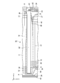
- the present invention it is possible to provide a display device that is less likely to reduce the reliability of the scanning line driver. Further, according to one embodiment of the present invention, it is possible to provide a display device in which problems such as destruction of elements in the driver circuit and poor curing of the photocurable sealing material are unlikely to occur.
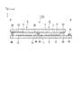
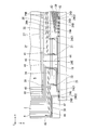
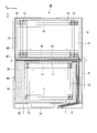
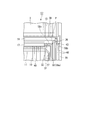
- FIG. 2 is a cross-sectional view taken along line AA ′ of FIG. It is a top view which shows the circuit structure of the peripheral part of a display apparatus.
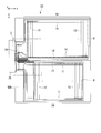
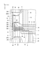
- FIG. 4 is an enlarged plan view of portions A and A ′ of FIG. 3.
- FIG. 4 is an enlarged plan view of a portion B in FIG. 3.
- It is a top view of the liquid crystal display device of 2nd Embodiment.
- It is a top view of the liquid crystal display device of 3rd Embodiment.
- It is a top view of the liquid crystal display device of 4th Embodiment.
- FIG. 1 is a plan view of the liquid crystal display device of the present embodiment.
- FIG. 2 is a cross-sectional view taken along line AA ′ of FIG.
- FIG. 3 is a plan view showing a circuit configuration of a peripheral portion of the liquid crystal display device.
- 4 is an enlarged plan view of portions A and A ′ of FIG.
- FIG. 5 is an enlarged plan view of a portion B in FIG.
- the scale of the size may be varied depending on the component.
- the liquid crystal display device 1 of the present embodiment includes an array substrate 2, a counter substrate 3, and a sealing material 4 ⁇ / b> A that bonds the array substrate 2 and the counter substrate 3 at a predetermined interval. , 4B and a liquid crystal panel 6 enclosed in a space surrounded by the array substrate 2, the counter substrate 3, and the sealing materials 4A, 4B.
- the liquid crystal display device 1 includes a backlight, a pair of polarizing plates, and the like as long as it is a transmissive liquid crystal display device.
- the liquid crystal layer of this embodiment corresponds to a “display medium” in the claims.
- the liquid crystal display device 1 has a configuration in which the first display unit 8 and the second display unit 9 are arranged side by side in one direction (y-axis direction in FIG. 1).
- the sealing material is composed of a first sealing material 4A that surrounds the outer periphery of the first display portion 8 and a second sealing material 4B that surrounds the outer periphery of the second display portion 9.
- a vertical electric field type liquid crystal display device such as a vertical alignment mode (VA mode) is assumed.
- VA mode vertical alignment mode
- the 1st display part 8 and the 2nd display part 9 can display independently.
- the liquid crystal display device 1 is suitable for use in, for example, a game machine or a portable electronic device as a so-called two-screen type liquid crystal display device.
- the first display unit 8 includes a plurality of first gate lines 10 and a plurality of first data lines 11.
- the plurality of first gate lines 10 extend in the arrangement direction of the first display unit 8 and the second display unit 9 (y-axis direction in FIG. 1).
- the plurality of first data lines 11 extend in a direction (x-axis direction in FIG. 1) orthogonal to the arrangement direction of the first display unit 8 and the second display unit 9.
- First pixel electrodes 12 are respectively provided in regions surrounded by the adjacent first gate lines 10 and the adjacent first data lines 11.
- the first display unit 8 includes a plurality of first pixel electrodes 12 arranged in a matrix.
- a first thin film transistor 7 for switching pixels (Thin Film Transistor, hereinafter abbreviated as TFT) is provided.
- the first TFT 7 is connected to the first gate line 10 and the first data line 11.
- the first pixel electrode 12 is connected to the first TFT 7. Therefore, the first pixel electrode 12 is connected to the first gate line 10 and the first data line 11 via the first TFT 7.
- the first pixel electrode 12 may be indirectly connected to the first TFT 7 via a TFT different from the first TFT 7 or a capacitive element.
- the second display unit 9 includes a plurality of second gate lines 13 and a plurality of second data lines 14.
- the plurality of second gate lines 13 extend in the arrangement direction of the first display unit 8 and the second display unit 9 (y-axis direction in FIG. 1).
- the plurality of second data lines 14 extend in a direction (x-axis direction in FIG. 1) orthogonal to the arrangement direction of the first display unit 8 and the second display unit 9.
- Second pixel electrodes 15 are respectively provided in regions surrounded by the adjacent second gate lines 13 and the adjacent second data lines 14.
- the second display unit 9 includes a plurality of second pixel electrodes 15 arranged in a matrix. In the vicinity of the intersection of the second gate line 13 and the second data line 14, a second TFT 16 for pixel switching is provided.
- the second TFT 16 is connected to the second gate line 13 and the second data line 14.
- the second pixel electrode 15 is connected to the second TFT 16. Therefore, the second pixel electrode 15 is connected to the second gate line 13 and the second data line 14 via the second TFT 16.
- the second pixel electrode 15 may be indirectly connected to the second TFT 16 via a TFT different from the second TFT 16 or a capacitive element.
- the first gate driver 17 is formed in a region sandwiched between the first display unit 8 and the second display unit 9.
- the first gate driver 17 has a function of supplying a gate signal to the plurality of first gate lines 10 of the first display unit 8.
- the dimension of the first gate driver 17 in the x-axis direction is substantially equal to the dimension of the first display unit 8 in the x-axis direction.
- a part of the second gate driver 18 is formed in a region sandwiched between the first display unit 8 and the second display unit 9.
- the second gate driver 18 has a function of supplying a gate signal to the plurality of second gate lines 13.
- the dimension of the second gate driver 18 in the x-axis direction is substantially the same as the dimension of the second display unit 9 in the x-axis direction.
- the dimension of the first display unit 8 in the x-axis direction is smaller than the dimension of the second display unit 9 in the x-axis direction. Therefore, the central part of the second gate driver 18 is formed in a region sandwiched between the first display unit 8 and the second display unit 9. The end of the second gate driver 18 protrudes to the left and right of the region sandwiched between the first display unit 8 and the second display unit 9.
- Each of the first gate driver 17 and the second gate driver 18 includes a TFT (not shown) monolithically formed on one surface of the array substrate 2. More specifically, each of the first gate driver 17 and the second gate driver 18 includes a plurality of stages of shift registers (not shown), and the shift registers include TFTs monolithically formed on one surface of the array substrate 2. Has been.
- the first sealing material 4 ⁇ / b> A and the second sealing material 4 ⁇ / b> B and the first gate driver 17 and the second gate driver 18 do not overlap in plan view when viewed from the normal direction of the counter substrate 3. Is arranged.
- the portion where the first sealing material 4A and the second sealing material 4B extend in parallel is disposed in a region sandwiched between the first gate driver 17 and the second gate driver 18.
- the shapes of the array substrate 2 and the counter substrate 3 are both rectangular.
- the length of one side of the array substrate 2 (side extending in the y-axis direction) is longer than the length of the corresponding side of the counter substrate 3. Therefore, the lower end of the array substrate 2 protrudes outside the lower end of the counter substrate 3.
- the portion of the array substrate 2 that projects to the outside of the counter substrate 3 is hereinafter referred to as a projecting portion 2h.
- the first display unit 8 is arranged on the side of the array substrate 2 close to the projecting part 2h, and the second display unit 9 is arranged on the side far from the projecting part 2h.
- a data driver 19 is mounted on the projecting portion 2 h of the array substrate 2.
- the data driver 19 has a function of supplying data signals to the first data line 11 and the second data line 14.
- the data driver 19 is mounted on the array substrate 2 in the form of an IC chip.
- the surface of the array substrate 2 and the counter substrate 3 on the side in contact with the liquid crystal layer 5 is referred to as “inner surface”, and the surface of the array substrate 2 and the counter substrate 3 on the side opposite to the side in contact with the liquid crystal layer 5 is referred to as “outer surface”.
- a plurality of first pixel electrodes 12 and a plurality of second pixel electrodes 15 are provided on the inner surface of the array substrate 2.
- the first pixel electrode 12 and the second pixel electrode 15 are made of a transparent conductive film such as indium tin oxide (hereinafter, abbreviated as ITO).
- a first gate driver 17 and a second gate driver 18 are provided at the center of the inner surface of the array substrate 2.
- a light shielding film 20 called a black matrix is provided on the inner surface of the counter substrate 3.
- a first counter electrode 21 is provided on the inner surface of the counter substrate 3 so as to face the plurality of first pixel electrodes 12.
- a second counter electrode 22 is provided on the inner surface of the counter substrate 3 so as to face the plurality of second pixel electrodes 15.
- a region where the plurality of first pixel electrodes 12 are arranged in a matrix is a region that substantially contributes to display, and this region is referred to as a first display unit 8.
- a region where the plurality of second pixel electrodes 15 are arranged in a matrix is a region that contributes substantially to display, and this region is referred to as a second display unit 9.
- the light shielding film 20 is provided in a portion excluding the first display unit 8 and the second display unit 9. In other words, the light shielding film 20 has an opening corresponding to the first display unit 8 and the second display unit 9. In FIG. 1, a portion where the light shielding film 20 is disposed is shown by shading.
- the light shielding film 20 overlaps the first gate driver 17 and the second gate driver 18 in a planar manner.
- the incidence of external light on the TFTs constituting the shift registers of the first gate driver 17 and the second gate driver 18 is suppressed.
- a shift in TFT characteristics can be suppressed and off-leakage current can be reduced.
- the above configuration is particularly applicable to a bottom gate TFT using an amorphous semiconductor or an oxide semiconductor (InGaZnO) composed of indium (In), gallium (Ga), and zinc (Zn) as a channel layer of the TFT. Is preferred.
- the light shielding film 20 is provided in a lattice shape in a region overlapping the first gate line 10, the first data line 11, and the first TFT of the first display unit 8.
- the light shielding film 20 is provided in a lattice shape in a region overlapping the second gate line 13, the second data line 14, and the second TFT of the second display unit 9.
- illustration of the lattice-shaped light shielding film in each of the display units 8 and 9 is omitted.
- FIG. 3 is a diagram showing a driving circuit and a wiring group in the peripheral portion of the array substrate 2 that is hidden under the light shielding film 20 from which the light shielding film 20 is omitted.
- a plurality of external connection terminals 24 are provided on the projecting portion 2h of the array substrate 2.
- a flexible printed wiring board 25 Flexible Printed Circuit, hereinafter abbreviated as FPC
- FPC Flexible Printed Circuit
- an electronic component such as a controller IC is mounted on the FPC 25, and various signals are output from the controller IC.
- the first display unit 8 includes 320 first gate lines 10 and 720 first data lines 11.
- One pixel is composed of three dots of red (R), green (G), and blue (B), and a first data line 11 is provided for each dot. Therefore, the number of pixels of the first display unit 8 is 320 ⁇ 240.
- the second display unit 9 includes 400 second gate lines 13 and 720 second data lines 14.
- the number of pixels of the second display unit 9 is 400 ⁇ 240.
- the distance between the adjacent first data lines 11 is the same as the distance between the adjacent second data lines 14.
- the distance between adjacent first gate lines 10 and the distance between adjacent second gate lines 13 are the same. That is, the pixel size of the first display unit 8 and the pixel size of the second display unit 9 are the same.
- the array substrate 2 includes a first data lead line group (wiring group surrounded by a broken line 27 in FIG. 3) and a second data lead line group (wiring group surrounded by a broken line 28 in FIG. 3). , And a first gate driver signal line group and a second gate driver signal line group (a wiring group collectively surrounded by a broken line 29 in FIG. 3).
- the array substrate 2 includes the above four types of wiring groups.
- the first data lead line group 27 includes a plurality of first data lead lines 32 that connect the first data line 11 and the first data line terminal 31 (see FIG. 5). Yes.
- the second data lead line group 28 includes a plurality of second data lead lines 34 connecting the second data line 14 and the second data line terminal 33 (see FIG. 5).
- the first gate driver signal line group 29A is composed of a plurality of first gate driver signal lines 35 that connect the first gate driver 17 and the external connection terminal 24A (see FIG. 5).
- the second gate driver signal line group 29B is composed of a plurality of second gate driver signal lines 36 that connect the second gate driver 18 and the external connection terminal 24B (see FIG. 5).
- the size of the first display unit 8 in the x-axis direction is larger than the size of the second display unit 9 in the x-axis direction due to the difference in the number of pixels (number of gate lines) as described above. small. Therefore, the width W1 (dimension in the x-axis direction) of the left and right frame regions G1 of the first display unit 8 is wider than the width W2 (dimension in the x-axis direction) of the left and right frame regions G2 of the second display unit 9. Therefore, the first display unit 8 is arranged on the lower side, that is, on the side close to the data driver 19 and the FPC 25, and the above four types of wiring groups are arranged in the left and right frame regions G1 of the first display unit 8. . The reason for this arrangement will be described later.
- the plurality of second data lead lines 34 are drawn from the left side of the second display unit 9 and are the left side of the two sides facing the x-axis direction of the array substrate 2. It is arranged in the frame area G1, G2 on the (first side) side.
- the plurality of first data lead lines 32 are drawn from the right side of the first display unit 8 and are arranged in the frame region G1 on the right side (second side) side of the two sides facing the x-axis direction of the array substrate 2.
- the plurality of first gate driver signal lines 35 are drawn from the right side of the first gate driver 17 and arranged in the frame region G1 on the right side.
- the plurality of second gate driver signal lines 36 are drawn from the right side of the second gate driver 18 and arranged in the frame region G1 on the right side.
- the plurality of second data lead lines 34 are disposed in the frame regions G1 and G2 on the left side, the plurality of first data lead lines 32, the plurality of first gate driver signal lines 35, and the plurality of second gates.
- the driver signal line 36 is disposed in the frame region G1 on the right side.
- the first gate driver signal line 35 and the second gate driver signal line 36 include, for example, a clock wiring, a start pulse wiring, a low potential wiring, an initialization wiring, and the like.
- the low potential wiring supplies a low level signal to each gate line.
- the initialization wiring periodically supplies an initial potential to a specific electrode in the gate driver.
- a second Cs line 38 is provided between two adjacent second gate lines 13.
- the second Cs line 38 is a wiring for forming a storage capacitor (storage capacitor) in each pixel in the second display unit 9.
- Second Cs lead lines 39 are provided in the frame regions G1 and G2 on the left side and the right side of the array substrate 2. The upper end of the second Cs lead line 39 is connected to the second Cs line 38. As shown in FIG. 5, the lower end of the second Cs lead line 39 is connected to the external connection terminal 24C2.
- the first Cs line 40 is provided between two adjacent first gate lines 10.
- the first Cs line 40 is a wiring for forming a storage capacitor (storage capacitor) in each pixel in the first display unit 8.
- the first Cs lead line 41 is provided in the frame region on the lower side of the array substrate 2.
- the upper end of the first Cs lead line 41 is connected to the first Cs line 40, and the lower end is connected to the external connection terminal 24C1.
- components corresponding to the Cs line and the Cs lead line may not exist.
- the storage capacitor storage capacitor
- the transparent electrode ITO or the like
- the transparent electrode is electrically connected to the Cs lead line at the periphery of the display unit.
- second common lead lines 42 are provided in the frame regions G ⁇ b> 1 and G ⁇ b> 2 on the left side and the right side of the array substrate 2.
- the second common lead line 42 is connected to the second counter electrode 22 (see FIG. 2) via the second common transition 43.
- the second common transition 43 is a member that electrically connects the second common lead line 42 on the array substrate 2 side and the second counter electrode 22 on the counter substrate 3 side.
- the second common transition 43 is provided at a plurality of locations on the second counter electrode 22.
- the specific configuration of the second common transition 43 is gold particles, conductive particles such as silver particles mixed in the sealing material, or carbon paste.
- the plurality of second common lead lines 42 are respectively connected to the external connection terminals 24D.
- a first common lead line 44 is provided in the frame area on the lower side of the array substrate 2.
- the first common lead line 44 is connected to the first counter electrode 21 (see FIG. 2) via the first common transition 45.
- the first common transition 45 is a member that electrically connects the first common lead line 44 on the array substrate 2 side and the first counter electrode 21 on the counter substrate 3 side.
- the specific configuration of the first common transition 45 is the same as that of the second common transition 43.
- the lower end of the first common lead wire 44 is connected to the external connection terminal 24E.
- a first data line terminal 31 for connecting the first data lead line 32 to the data driver 19 is provided on the right side of the area corresponding to the data driver 19 on the array substrate 2.
- a second data line terminal 33 for connecting the second data lead-out line 34 to the data driver 19 is provided on the left side of the area corresponding to the data driver 19 on the array substrate 2.
- a plurality of external connection terminals 24A for the first gate driver signal lines 35 and external connection terminals for the plurality of second gate driver signal lines 36 are provided. 24B.
- the first gate driver 17 and the second gate driver 18 are formed in a region sandwiched between the first display unit 8 and the second display unit 9. That is, the first gate driver 17 and the second gate driver 18 are arranged not at the peripheral edge of the array substrate 2 but at substantially the center of the array substrate 2. Therefore, moisture hardly enters the first gate driver 17 and the second gate driver 18, and the reliability of the gate driver is not easily reduced due to wiring corrosion and a decrease in the element performance of the driver circuit.
- first gate driver 17 and the second gate driver 18 are not arranged immediately below the first seal material 4A and the second seal material 4B. Therefore, even when narrowing the frame of the liquid crystal display device 1, it is possible to avoid the stress from the first seal material 4A and the second seal material 4B from being applied to the TFTs of the first gate driver 17 and the second gate driver 18. . As a result, it is possible to realize a gate driver that suppresses the breakdown of the TFT and has excellent reliability.
- the sealing material 4A and the second sealing material 4B even when a photo-curing type sealing material such as ultraviolet light is used as the first sealing material 4A and the second sealing material 4B, the light is blocked by the pattern of the first gate driver 17 and the second gate driver 18. It will not be done. Therefore, the sealing material can be more reliably cured in the manufacturing process of the liquid crystal display device 1.
- a photo-curing type sealing material such as ultraviolet light
- the first display unit 8 having a small size in the left-right direction (x-axis direction) is placed on the side close to the overhanging portion 2h of the array substrate 2, that is, on the side close to the region where the data driver 19 and the FPC 25 are mounted. It is preferable to arrange the liquid crystal display device 1 in order to narrow the frame. The reason is as follows.
- various wirings are concentrated in an area close to the data driver 19 and the FPC 25.
- the first gate driver 17 and the second gate driver 18 are arranged in the approximate center of the array substrate 2, so that a large number of first gate driver signal lines 35 and second gate driver signal lines are provided.
- An area for arranging 36 is required. In this case, if the dimension in the x-axis direction of the first display unit 8 close to the area where the data driver 19 and the FPC 25 are mounted is small, margins are formed on the left and right sides of the first display unit 8.
- the first gate driver signal line 35 and the second gate driver signal line 36 may be disposed in the margin.
- the first gate driver signal line 35 and the second gate driver are arranged on the left and right sides of the second display unit 9. It is necessary to add an area in which the signal line 36 is disposed. In that case, it becomes difficult to narrow the frame.
- the second data lead line 34 of the second display unit 9 located far from the data driver 19 is arranged in the frame area on the left side, but the other first data lead lines 32, The first gate driver signal line 35 and the second gate driver signal line 36 are not arranged in the frame region on the left side.
- the reason for this arrangement is that the second data lead-out line 34 is longer than the first data lead-out line 32, so that signal delay, blunting, or disconnection is likely to occur. Therefore, it is preferable to secure an area for making the second data lead-out line 34 thicker than other wirings.
- the width of the second data lead-out line 34 is different between the side of the second display unit 9 and the side of the first display unit 8.
- the width of the second data lead line 34 is, for example, 4 ⁇ m on the side of the second display unit 9, and is, for example, 6 ⁇ m on the side of the first display unit 8.
- the first data lead line 32 and the second data lead line 34 are formed with different lead lines in different layers. Thereby, the wiring pitch in the same layer can be expanded.
- the first common lead wire 44 connects the external connection terminal 24E and the first common transition 45 with the shortest distance.
- the delay or dullness of the common signal supplied to the first counter electrode 21 can be reduced, and the number of first common transitions 45 can be reduced.
- FIG. 6 is a plan view showing the liquid crystal display device of the present embodiment.
- the same components as those in FIG. 1 of the first embodiment are denoted by the same reference numerals, and detailed description thereof is omitted.
- the sealing material is composed of the first sealing material 4A and the second sealing material 4B that individually surround the outer periphery of the first display portion 8 and the second display portion 9.
- the part of the side facing the first display portion 8 is shared by one sealing material 4C.
- the shared portion of the sealing material 4 ⁇ / b> C is disposed at a position that does not overlap the first gate driver 17 and the second gate driver 18. All the sealing materials 4A, 4B, 4C may be integrated. Other configurations are the same as those of the first embodiment.
- the liquid crystal layer 5 is divided by forming a sealing material at the boundary between the first display unit 8 and the second display unit 9. It is preferable.
- FIG. 7 is a plan view showing the liquid crystal display device of the present embodiment.
- the same components as those in FIG. 1 of the first embodiment are denoted by the same reference numerals, and detailed description thereof is omitted.
- the liquid crystal display device 51 of the present embodiment is provided with a sealing material 4 ⁇ / b> D that collectively surrounds the outer periphery of the first display unit 8 and the second display unit 9. Therefore, the liquid crystal layer 5 (see FIG. 2) is not divided between the first display unit 8 and the second display unit 9.
- the sealing material 4D is not disposed in the central portion of the liquid crystal display device 51, and therefore does not overlap the first gate driver 17 and the second gate driver 18.
- Other configurations are the same as those of the first embodiment.
- the pattern of the sealing material of the first to third embodiments may be appropriately selected according to the size of the liquid crystal panel, the method of forming the sealing material, the method of injecting the liquid crystal, and the like.
- the method for forming the sealing material include a printing method using a screen plate and a coating method using a dispenser.
- the liquid crystal injection method include a liquid crystal dropping method and a vacuum injection method from an injection port.
- FIG. 8 is a plan view showing the liquid crystal display device of the present embodiment.
- FIG. 9 is an enlarged view of a portion C in FIG. 8 and 9, the same reference numerals are given to the same components as those in FIG. 3 of the first embodiment, and detailed description thereof will be omitted.
- both the array substrate 55 and the counter substrate 56 are rectangular.
- the length of one side of the array substrate 55 (side extending in the x-axis direction) is longer than the length of the corresponding side of the counter substrate 56.
- the left end of the array substrate 55 projects outside the left end of the counter substrate 56.
- the arrangement direction of the first display unit 8 and the second display unit 9 is the y-axis direction as in the first embodiment.
- the data driver 19 and the FPC 25 are mounted on the protruding portion 55 h at the left end of the array substrate 55. This configuration is suitable when it is desired to make the vertical frame size smaller than the horizontal frame size.
- the plurality of first gate driver signal lines 35 are led out from the left end of the first gate driver 17, extend to the left side, and are connected to the first gate driver signal line terminal 24A. ing.
- the plurality of second gate driver signal lines 36 are led out from the left end of the second gate driver 18, extend to the left side, and are connected to the second gate driver signal line terminal 24 ⁇ / b> B.
- a part of the plurality of first gate driver signal lines 35 and a part of the plurality of second gate driver signal lines 36 include a plurality of first data line terminals 31 and a plurality of second data line terminals 33. It is arranged in a region sandwiched between.
- the distances between the first gate driver 17 and the second gate driver 18 and the FPC 25 are short, and the first gate driver signal line 35 and the second gate driver signal line 36 are connected to the external connection terminals 24A. 24B and the gate drivers 17 and 18 are connected with the shortest distance. With this configuration, delay and dullness of the gate signal can be reduced.
- FIG. 10 is a plan view showing a main part of the liquid crystal display device of the present embodiment.
- FIG. 10 shows a portion corresponding to the portion A ′ of FIG. 4 used in the first embodiment. 10, the same code
- the low potential wiring 58 of the first gate driver signal line 35 and the second gate driver signal line 36 is connected to the first gate driver 17 and the first gate driver 17. It is shared by the two gate drivers 18.
- the low potential wiring 58 includes one main line 58a extending from the external connection terminal and a branch line 58b in which the main line 58a branches into two at the branch point P immediately before the first gate driver 17 and the second gate driver 18. Have.
- Each branch line 58 b is connected to the first gate driver 17 or the second gate driver 18.
- the low potential wiring 58 is a wiring for supplying a low level signal to the gate line. That is, among the plurality of first gate driver signal lines 35 and the plurality of second gate driver signal lines 36, the first gate driver 17 and the second gate driver 18 share a signal line having the same function. ing. Other configurations are the same as those of the first embodiment.
- the frame of the liquid crystal display device 57 can be further reduced.
- the number of FPC connection terminals can be reduced, so that the width of the FPC 25 can be reduced.
- the liquid crystal module including the FPC 25 can be downsized.
- the first gate driver 17 and the second gate driver 18 may share other wirings, such as the initialization wiring, without being limited to the low potential wiring 58. In order to realize these configurations, it is necessary to match the drive timing between the first display unit 8 and the second display unit 9.
- FIG. 11 is a plan view showing the liquid crystal display device of the present embodiment.
- FIG. 12 is an enlarged view of a portion D in FIG. 11 and 12, the same reference numerals are given to the same components as those in FIGS. 3 and 4 of the first embodiment, and detailed description thereof will be omitted.
- the liquid crystal display device 1 of the first embodiment separately includes the first gate driver 17 for the first display unit and the second gate driver 18 for the second display unit.
- the liquid crystal display device 61 of this embodiment supplies a gate signal to the first gate line 10 of the first display unit 8 and the second gate line 13 of the second display unit 9.
- a gate driver 62 is provided. That is, the first display unit 8 and the second display unit 9 share one gate driver 62.
- the gate driver 62 includes a plurality of stages of shift registers (not shown), and the shift registers include TFTs (not shown) monolithically formed on the array substrate 2.
- a part of the gate driver 62 is formed in a region sandwiched between the first display unit 8 and the second display unit 9.
- illustration of the sealing material is omitted in FIG. 11, also in this embodiment, the sealing material and the gate driver 62 are arranged at positions where they do not overlap in plan view.
- a plurality of gate driver signal lines 63 are also included in the first display unit 8 and the second display unit. 9 and shared.
- the plurality of gate driver signal lines 63 are led out from the right end of the gate driver 62, arranged along the right side of the array substrate 2, and connected to the external connection terminal 24.
- the first display unit 8 and the second display unit 9 share an output TFT that outputs a gate signal to each gate line.
- the number of the second gate lines 13 of the second display unit 9 is larger than the number of the first gate lines 10 of the first display unit 8. Therefore, the output TFT connected to both the first gate line 10 and the second gate line 13 and the output TFT connected only to the second gate line 13 are present in the plurality of output TFTs. Become. For example, if the number of the first gate lines 10 is 320 and the number of the second gate lines 13 is 400, out of 400 output TFTs, 320 output TFTs are the first gate line 10 and the second gate line 13. The 80 output TFTs connected to both are connected only to the second gate line 13.
- a load capacitance adjusting unit 64 is connected to each of the output TFTs (not shown) connected only to the second gate line 13.
- the load capacitance adjusting unit 64 can be realized, for example, by overlapping the second Cs lead line 39 and the drain electrode of the output TFT (electrode on the side connected to the gate line) via a gate insulating film.
- the output TFT connected to two gate lines and the output TFT connected to one gate line have different load capacitances.
- the way in which the delay or dullness of the gate signal occurs differs, and a luminance difference may occur due to a difference in the charge amount to each pixel capacitance or a difference in feedthrough voltage.
- the load capacitance adjusting unit 64 can be connected to an output TFT connected to one gate line, so that the load capacitances of both can be made substantially coincident. As a result, the effect of suppressing the block-like luminance difference can be obtained.
- the load capacitance adjusting unit 64 is not necessary. Other configurations are the same as those of the first embodiment.
- the gate driver signal line 63 is shared by the first display unit 8 and the second display unit 9, and therefore, the region where the gate driver signal line 63 is arranged is compared with the first embodiment. Can be narrowed. As a result, both the vertical and horizontal frame regions can be narrowed. Further, since the total number of gate driver signal lines 63 is reduced, the number of external connection terminals 24 can be reduced, so that the width of the FPC 25 can be reduced. Thereby, the liquid crystal module including the FPC 25 can be downsized. When realizing the configuration of the present embodiment, it is necessary to match the drive timing between the first display unit 8 and the second display unit 9.
- FIG. 13 is a plan view showing the liquid crystal display device of the present embodiment.
- the same components as those in FIG. 11 of the sixth embodiment are denoted by the same reference numerals, and detailed description thereof is omitted.
- the liquid crystal display device 67 of this embodiment is the same as that of the sixth embodiment in that the first display unit 8 and the second display unit 9 share one gate driver 69.
- the sixth embodiment is different from the sixth embodiment in that the output portion of the gate driver 69 is divided into a first gate line output portion 68A and a second gate line output portion 68B.
- the right part of the gate driver 69 is assigned to the first gate line output unit 68A
- the left part of the gate driver 69 is assigned to the second gate line output unit 68B. Therefore, all the first gate lines 10 are drawn out only from the right part of the gate driver 69, and all the second gate lines 13 are drawn out only from the left part of the gate driver 69.
- Other configurations are the same as those of the sixth embodiment.
- an oxide semiconductor composed of indium (In), gallium (Ga), and zinc (Zn) is used for the channel layer of the output TFT in the gate driver 69 and the TFT in the pixel region. It is suitable for use. The reason is that in the case of a TFT using an InGaZnO oxide semiconductor, the on-current is large, the off-current is small, and the TFT size can be reduced.
- the technical scope of the present invention is not limited to the above embodiment, and various modifications can be made without departing from the spirit of the present invention.
- the first display unit and the second display unit may have the same number of pixels, different pixel sizes, and different areas of the first display unit and the second display unit.
- the first display unit and the second display unit may have the same number of gate lines and different numbers of data lines.
- the first display unit and the second display unit may have different numbers of gate lines and data lines.
- the data driver that outputs the data signal to the first data line and the data driver that outputs the data signal to the second data line are configured by one data driver.
- the data driver that outputs the data signal to the first data line and the data driver that outputs the data signal to the second data line may be separate data drivers. That is, a configuration in which two data drivers are mounted on the array substrate may be employed.
- a plurality of data drivers may be provided for one display unit.
- the number, arrangement, shape, and the like of various circuits and wirings are not limited to the above embodiment, and can be changed as appropriate.
- the display device of the present invention is not limited to a liquid crystal display device, and may be, for example, an electronic paper using a microcapsule enclosing white charged particles and black charged particles as a display medium.
- the display device of the present invention may be an organic electroluminescence display device that uses an organic light-emitting layer that emits light by charge injection as a display medium.
- the present invention is applicable to various display devices such as liquid crystal display devices, electronic paper, and organic electroluminescence display devices.
- Light shielding film 21 ... First counter electrode, 22 ... second counter electrode, 32 ... first data lead line, 34 ... second data lead line, 35 ... first gate driver signal line, 36 ... second gate driver signal line, 44 ... First common lead wire, 58 ... low potential Line, 62 and 69 ... gate driver, 63 ... gate driver signal line, 64 ... load capacitance adjusting unit, 68A ... output unit for the first gate line, 68B ... output section for the second gate line.
Landscapes
- Physics & Mathematics (AREA)
- Nonlinear Science (AREA)
- Chemical & Material Sciences (AREA)
- Crystallography & Structural Chemistry (AREA)
- General Physics & Mathematics (AREA)
- Mathematical Physics (AREA)
- Optics & Photonics (AREA)
- Engineering & Computer Science (AREA)
- Liquid Crystal (AREA)
- Computer Hardware Design (AREA)
- Theoretical Computer Science (AREA)
- Devices For Indicating Variable Information By Combining Individual Elements (AREA)
Abstract
Description
本願は、2013年1月30日に、日本に出願された特願2013-015727号に基づき優先権を主張し、その内容をここに援用する。
前記データドライバが、矩形状の前記アレイ基板の前記配列方向と直交する方向に対向する2辺のうちの第1辺に実装されてもよい。
前記第1ゲートドライバ用信号線の一部および前記第2ゲートドライバ用信号線の一部が、前記アレイ基板の一面における複数の第1データライン用端子群と複数の第2データライン用端子群とに挟まれた領域に配置されてもよい。
以下、本発明の第1実施形態について、図1~図5を用いて説明する。
本実施形態では、表示装置として液晶表示装置の一例を挙げて説明する。
図1は、本実施形態の液晶表示装置の平面図である。図2は、図1のA-A‘線に沿った断面図である。図3は、液晶表示装置の周縁部の回路構成を示す平面図である。図4は、図3のAおよびA’部分の拡大平面図である。図5は、図3のB部分の拡大平面図である。
なお、以下の各図面においては各構成要素を見やすくするため、構成要素によって寸法の縮尺を異ならせて示すことがある。
言い換えると、遮光膜20は、第1表示部8および第2表示部9に対応する部分が開口している。図1では、遮光膜20が配置された箇所を網かけで示している。
また、隣り合う第1データライン11間の距離と、隣り合う第2データライン14間の距離と、は同じである。隣り合う第1ゲートライン10間の距離と、隣り合う第2ゲートライン13間の距離と、は同じである。すなわち、第1表示部8の画素サイズと、第2表示部9の画素サイズと、は同じである。
第1ゲートドライバ用信号線群29Aは、第1ゲートドライバ17と外部接続端子24A(図5参照)とを接続する複数の第1ゲートドライバ用信号線35で構成されている。第2ゲートドライバ用信号線群29Bは、第2ゲートドライバ18と外部接続端子24B(図5参照)とを接続する複数の第2ゲートドライバ用信号線36で構成されている。
以下、本発明の第2実施形態について、図6を参照して説明する。
本実施形態の液晶表示装置の基本構成は第1実施形態と同様であり、シール材の構成が第1実施形態と異なる。
図6は、本実施形態の液晶表示装置を示す平面図である。
図6において、第1実施形態の図1と共通の構成要素には同一の符号を付し、詳細な説明を省略する。
以下、本発明の第3実施形態について、図7を参照して説明する。
本実施形態の液晶表示装置の基本構成は第1実施形態と同様であり、シール材の構成が第1実施形態と異なる。
図7は、本実施形態の液晶表示装置を示す平面図である。
図7において、第1実施形態の図1と共通の構成要素には同一の符号を付し、詳細な説明を省略する。
以下、本発明の第4実施形態について、図8、図9を参照して説明する。
本実施形態の液晶表示装置の基本構成は第1実施形態と同様であり、両基板の形状、およびデータドライバとFPCの配置が第1実施形態と異なる。
図8は、本実施形態の液晶表示装置を示す平面図である。図9は、図8のC部分の拡大図である。
図8、図9において、第1実施形態の図3と共通の構成要素には同一の符号を付し、詳細な説明を省略する。
以下、本発明の第5実施形態について、図10を参照して説明する。
本実施形態の液晶表示装置の基本構成は第1実施形態と同様であり、ゲートドライバ用信号線の一部が第1実施形態と異なる。
図10は、本実施形態の液晶表示装置の要部を示す平面図である。図10は、第1実施形態で用いた図4のA‘部分に対応する箇所を示している。
図10において、第1実施形態の図4と共通の構成要素には同一の符号を付し、詳細な説明を省略する。
以下、本発明の第6実施形態について、図11、図12を参照して説明する。
本実施形態の液晶表示装置の基本構成は第1実施形態と同様であり、ゲートドライバの構成が第1実施形態と異なる。
図11は、本実施形態の液晶表示装置を示す平面図である。図12は、図11のD部分の拡大図である。
図11、図12において、第1実施形態の図3、図4と共通の構成要素には同一の符号を付し、詳細な説明を省略する。
なお、第1ゲートライン10の本数と第2ゲートライン13の本数が等しい場合には負荷容量調整部64は不要である。その他の構成は第1実施形態と同様である。
以下、本発明の第7実施形態について、図13を参照して説明する。
本実施形態の液晶表示装置の基本構成は第6実施形態と同様であり、ゲートドライバの構成が第1実施形態と異なる。
図13は、本実施形態の液晶表示装置を示す平面図である。
図13において、第6実施形態の図11と共通の構成要素には同一の符号を付し、詳細な説明を省略する。
例えば上記実施形態では、第1表示部と第2表示部とでゲートラインの本数および画素数が異なる例を挙げたが、本発明はこれに限るものではない。例えば、第1表示部と第2表示部とで画素数が等しく、画素サイズが異なり、第1表示部の面積と第2表示部の面積とが異なる構成であってもよい。もしくは、第1表示部と第2表示部とでゲートラインの本数が等しく、データラインの本数が異なる構成であってもよい。もしくは、第1表示部と第2表示部とでゲートラインの本数、データラインの本数がともに異なる構成であってもよい。
Claims (18)
- 第1表示部と第2表示部とが一面に並んで配置されたアレイ基板を備え、
前記第1表示部が、前記第1表示部と前記第2表示部との配列方向に延在する複数の第1ゲートラインと、前記配列方向と交差する方向に延在する複数の第1データラインと、前記第1ゲートラインと前記第1データラインとに接続された第1薄膜トランジスタと、前記第1薄膜トランジスタに直接または間接的に接続された第1画素電極と、を備え、
前記第2表示部が、前記第1表示部と前記第2表示部との配列方向に延在する複数の第2ゲートラインと、前記配列方向と交差する方向に延在する複数の第2データラインと、前記第2ゲートラインと前記第2データラインとに接続された第2薄膜トランジスタと、前記第2薄膜トランジスタに直接または間接的に接続された第2画素電極と、を備え、
前記第1ゲートラインにゲート信号を供給する第1ゲートドライバおよび前記第2ゲートラインにゲート信号を供給する第2ゲートドライバの各々が、前記アレイ基板の一面に形成されたトランジスタを含んで構成され、
前記第1ゲートドライバの少なくとも一部および前記第2ゲートドライバの少なくとも一部が、前記第1表示部と前記第2表示部とに挟まれた領域に形成されている表示装置。 - 対向基板と、前記アレイ基板と前記対向基板とを所定の間隔をおいて貼り合わせるシール材と、前記アレイ基板と前記対向基板と前記シール材とにより囲まれた空間内に封入された表示媒体と、をさらに備える請求項1に記載の表示装置。
- 前記対向基板の法線方向から見て、前記シール材と前記第1ゲートドライバおよび前記第2ゲートドライバとが重ならない位置に配置される請求項2に記載の表示装置。
- 前記シール材が、前記第1表示部の外周を取り囲む第1シール材と、前記第2表示部の外周を取り囲む第2シール材と、を含む請求項3に記載の表示装置。
- 前記第1シール材のうちの前記第2表示部に面する部分と、前記第2シール材のうちの前記第1表示部に面する部分と、を一つのシール材で共用する請求項4に記載の表示装置。
- 前記シール材が、前記第1表示部および前記第2表示部の外周を一括して取り囲むシール材で構成される請求項3に記載の表示装置。
- 前記対向基板の一面に遮光層が設けられ、
前記対向基板の法線方向から見て、前記遮光層と前記第1ゲートドライバ、および前記遮光層と前記第2ゲートドライバが、重なった位置に配置される請求項2から請求項6までのいずれか一項に記載の表示装置。 - 前記第1ゲートラインの本数が前記第2ゲートラインの本数よりも少ない請求項2から請求項7までのいずれか一項に記載の表示装置。
- 前記第1データラインおよび前記第2データラインにデータ信号を供給するデータドライバが、矩形状の前記アレイ基板の前記配列方向に対向する2辺のうち、前記第1表示部に近い側の1辺に配置される請求項8に記載の表示装置。
- 前記アレイ基板が、前記第1データラインと第1データライン用端子とを接続する第1データ引き出し線と、前記第2データラインと第2データライン用端子とを接続する第2データ引き出し線と、前記第1ゲートドライバと外部接続端子とを接続する第1ゲートドライバ用信号線と、前記第2ゲートドライバと外部接続端子とを接続する第2ゲートドライバ用信号線と、をさらに備え、
前記第2データ引き出し線が、前記アレイ基板の前記配列方向と直交する方向に対向する2辺のうちの第1辺に配置され、
前記第1データ引き出し線、前記第1ゲートドライバ用信号線、および前記第2ゲートドライバ用信号線が、前記2辺のうちの第2辺に配置される請求項9に記載の表示装置。 - 前記アレイ基板が、前記第1表示部に対応する前記対向基板上の第1対向電極にコモン信号を供給する第1コモン引き出し線をさらに備え、
前記第1コモン引き出し線の一部が、前記アレイ基板の一面における複数の第1データライン用端子と複数の第2データライン用端子とに挟まれた領域に配置される請求項9または請求項10に記載の表示装置。 - 前記アレイ基板が、前記第1データラインおよび前記第2データラインに対してデータ信号を供給するデータドライバを備え、
前記データドライバが、矩形状の前記アレイ基板の前記配列方向と直交する方向に対向する2辺のうちの第1辺に実装される請求項2から請求項8までのいずれか一項に記載の表示装置。 - 前記アレイ基板が、前記第1ゲートドライバと外部接続端子とを接続する第1ゲートドライバ用信号線と、前記第2ゲートドライバと外部接続端子とを接続する第2ゲートドライバ用信号線と、をさらに備え、
前記第1ゲートドライバ用信号線の一部および前記第2ゲートドライバ用信号線の一部が、前記アレイ基板の一面における複数の第1データライン用端子と複数の第2データライン用端子とに挟まれた領域に配置される請求項12に記載の表示装置。 - 前記アレイ基板が、前記第1ゲートドライバと外部接続端子とを接続する複数の第1ゲートドライバ用信号線と、前記第2ゲートドライバと外部接続端子とを接続する複数の第2ゲートドライバ用信号線と、をさらに備え、
前記複数の第1ゲートドライバ用信号線および前記複数の第2ゲートドライバ用信号線のうち、前記第1ゲートドライバと前記第2ゲートドライバとで同一の機能を有する信号線が共有される請求項2から請求項13までのいずれか一項に記載の表示装置。 - 第1表示部と第2表示部とが一面に並んで配置されたアレイ基板を備え、
前記第1表示部が、前記第1表示部と前記第2表示部との配列方向に延在する複数の第1ゲートラインと、前記配列方向と交差する方向に延在する複数の第1データラインと、前記第1ゲートラインと前記第1データラインとに接続された第1薄膜トランジスタと、前記第1薄膜トランジスタに直接または間接的に接続された第1画素電極と、を備え、
前記第2表示部が、前記第1表示部と前記第2表示部との配列方向に延在する複数の第2ゲートラインと、前記配列方向と交差する方向に延在する複数の第2データラインと、前記第2ゲートラインと前記第2データラインとに接続された第2薄膜トランジスタと、前記第2薄膜トランジスタに直接または間接的に接続された第2画素電極と、を備え、
前記第1ゲートラインおよび前記第2ゲートラインにゲート信号を供給するゲートドライバが、前記アレイ基板の一面に形成されたトランジスタを含んで構成され、前記ゲートドライバの少なくとも一部が、前記第1表示部と前記第2表示部とに挟まれた領域に形成される表示装置。 - 前記第1ゲートラインの本数と前記第2ゲートラインの本数とが異なり、
前記ゲートドライバの複数の出力トランジスタのうち、一部の出力トランジスタに前記第1ゲートラインおよび前記第2ゲートラインの双方が接続され、残りの出力トランジスタに前記第1ゲートラインおよび前記第2ゲートラインのいずれか一方が接続され、
前記第1ゲートラインおよび前記第2ゲートラインのいずれか一方が接続された出力トランジスタに、負荷容量調整部が接続される請求項15に記載の表示装置。 - 前記ゲートドライバが、前記配列方向と交差する方向において、前記第1ゲートラインに接続された出力トランジスタを含む第1ゲートライン出力部と、前記第2ゲートラインに接続された出力トランジスタを含む第2ゲートライン出力部と、に分割される請求項15または請求項16に記載の表示装置。
- 前記トランジスタの半導体層が、インジウム、ガリウム、および亜鉛を含む酸化物半導体で構成される請求項1から請求項17までのいずれか一項に記載の表示装置。
Priority Applications (3)
| Application Number | Priority Date | Filing Date | Title |
|---|---|---|---|
| US14/764,198 US9443781B2 (en) | 2013-01-30 | 2014-01-24 | Display device |
| JP2014559651A JP6080316B2 (ja) | 2013-01-30 | 2014-01-24 | 表示装置 |
| CN201480006210.XA CN104956429B (zh) | 2013-01-30 | 2014-01-24 | 显示装置 |
Applications Claiming Priority (2)
| Application Number | Priority Date | Filing Date | Title |
|---|---|---|---|
| JP2013-015727 | 2013-01-30 | ||
| JP2013015727 | 2013-01-30 |
Publications (1)
| Publication Number | Publication Date |
|---|---|
| WO2014119478A1 true WO2014119478A1 (ja) | 2014-08-07 |
Family
ID=51262192
Family Applications (1)
| Application Number | Title | Priority Date | Filing Date |
|---|---|---|---|
| PCT/JP2014/051467 Ceased WO2014119478A1 (ja) | 2013-01-30 | 2014-01-24 | 表示装置 |
Country Status (4)
| Country | Link |
|---|---|
| US (1) | US9443781B2 (ja) |
| JP (1) | JP6080316B2 (ja) |
| CN (1) | CN104956429B (ja) |
| WO (1) | WO2014119478A1 (ja) |
Cited By (8)
| Publication number | Priority date | Publication date | Assignee | Title |
|---|---|---|---|---|
| KR20170047446A (ko) * | 2015-10-22 | 2017-05-08 | 삼성디스플레이 주식회사 | 플렉서블 표시 장치 |
| JP2019219629A (ja) * | 2018-06-22 | 2019-12-26 | パナソニック液晶ディスプレイ株式会社 | 表示装置 |
| JPWO2019021147A1 (ja) * | 2017-07-27 | 2020-07-27 | 株式会社半導体エネルギー研究所 | 表示パネル、表示装置、入出力装置、情報処理装置 |
| JP2020140039A (ja) * | 2019-02-27 | 2020-09-03 | 株式会社ジャパンディスプレイ | 表示装置 |
| JP2020140038A (ja) * | 2019-02-27 | 2020-09-03 | 株式会社ジャパンディスプレイ | 表示装置 |
| JP2021001926A (ja) * | 2019-06-20 | 2021-01-07 | 株式会社ジャパンディスプレイ | 表示装置 |
| JPWO2022234382A1 (ja) * | 2021-05-07 | 2022-11-10 | ||
| EP3196941B1 (en) * | 2014-09-16 | 2023-06-07 | BOE Technology Group Co., Ltd. | Array substrate and display device thereof |
Families Citing this family (15)
| Publication number | Priority date | Publication date | Assignee | Title |
|---|---|---|---|---|
| CN104956429B (zh) * | 2013-01-30 | 2017-10-03 | 夏普株式会社 | 显示装置 |
| US10255863B2 (en) * | 2014-04-02 | 2019-04-09 | Samsung Display Co., Ltd. | Display panel having a first region, a second region, and a third region between the first and second regions and including a drive portion on the third region |
| US10074323B2 (en) * | 2015-06-18 | 2018-09-11 | Panasonic Liquid Crystal Display Co., Ltd. | Liquid crystal display device and manufacturing method thereof |
| CN105259720B (zh) * | 2015-10-23 | 2018-11-27 | 深超光电(深圳)有限公司 | 阵列基板以及使用该阵列基板的显示面板 |
| KR102471672B1 (ko) | 2015-11-13 | 2022-11-29 | 삼성전자주식회사 | 표시 제어 방법, 이를 구현한 디스플레이 패널, 디스플레이 장치 및 전자 장치 |
| JP6847624B2 (ja) | 2016-10-14 | 2021-03-24 | 株式会社ジャパンディスプレイ | 表示装置 |
| JP2018128487A (ja) * | 2017-02-06 | 2018-08-16 | セイコーエプソン株式会社 | 電気光学パネル、電気光学装置および電子機器 |
| US10481447B2 (en) * | 2017-10-30 | 2019-11-19 | A.U. Vista, Inc. | LCD display device |
| JP2019113672A (ja) * | 2017-12-22 | 2019-07-11 | シャープ株式会社 | 表示制御装置、表示装置、および制御方法 |
| JP2021512371A (ja) * | 2018-02-01 | 2021-05-13 | マッカートニー, リチャードMCCARTNEY, Richard | カスタマイズされたディスプレイパネルを構築するための方法、システムおよび装置 |
| CN108322579A (zh) * | 2018-04-25 | 2018-07-24 | 维沃移动通信有限公司 | 一种移动终端 |
| CN109581755A (zh) * | 2018-12-18 | 2019-04-05 | 深圳市华星光电半导体显示技术有限公司 | 显示面板制造方法及显示面板 |
| US12347402B2 (en) * | 2019-01-09 | 2025-07-01 | HKC Corporation Limited | Display panel, driving method, and display device |
| CN116300217A (zh) * | 2023-03-20 | 2023-06-23 | 奇瑞汽车股份有限公司 | 一种多联显示屏及制备方法 |
| WO2025197176A1 (ja) * | 2024-03-19 | 2025-09-25 | ソニーグループ株式会社 | 表示装置 |
Citations (7)
| Publication number | Priority date | Publication date | Assignee | Title |
|---|---|---|---|---|
| JP2005196212A (ja) * | 2004-01-09 | 2005-07-21 | Samsung Electronics Co Ltd | 表示装置 |
| JP2010079314A (ja) * | 2009-12-25 | 2010-04-08 | Mitsubishi Electric Corp | 表示装置 |
| WO2011043440A1 (ja) * | 2009-10-08 | 2011-04-14 | シャープ株式会社 | 液晶表示装置およびその製造方法 |
| JP2011215380A (ja) * | 2010-03-31 | 2011-10-27 | Toppan Printing Co Ltd | 表示パネル、この表示パネルを利用した大型表示パネル |
| WO2012002042A1 (ja) * | 2010-06-30 | 2012-01-05 | シャープ株式会社 | 表示装置 |
| WO2012002043A1 (ja) * | 2010-06-30 | 2012-01-05 | シャープ株式会社 | 表示装置 |
| US20120194773A1 (en) * | 2011-02-01 | 2012-08-02 | Samsung Electronics Co., Ltd. | Display apparatus and display set having the same |
Family Cites Families (17)
| Publication number | Priority date | Publication date | Assignee | Title |
|---|---|---|---|---|
| JPS582641B2 (ja) | 1973-11-01 | 1983-01-18 | 株式会社クボタ | コンバインの引起し搬送装置 |
| JPS6075818A (ja) * | 1983-10-01 | 1985-04-30 | Jeco Co Ltd | 液晶表示装置 |
| US7006193B2 (en) * | 1999-05-10 | 2006-02-28 | Au Optronics Corporation | Method of sealing two substrates with a non-epoxy or epoxy-acrylate sealant using laser radiation |
| JP2001255513A (ja) * | 2000-03-13 | 2001-09-21 | Minolta Co Ltd | 液晶表示装置 |
| JP2001255514A (ja) | 2000-03-13 | 2001-09-21 | Minolta Co Ltd | 液晶表示装置 |
| JP2002148604A (ja) * | 2000-11-07 | 2002-05-22 | Matsushita Electric Ind Co Ltd | 液晶表示装置およびそれを用いた携帯型情報通信装置 |
| JP2003216116A (ja) | 2002-01-23 | 2003-07-30 | Sharp Corp | 表示装置およびその制御方法、ならびにそれを搭載した携帯情報機器 |
| JP2003216059A (ja) * | 2002-01-24 | 2003-07-30 | Sharp Corp | 表示素子およびその製造方法 |
| US20040263763A1 (en) * | 2002-01-28 | 2004-12-30 | Kyoritsu Chemical & Co., Ltd. | Sealing agent for LC dropping method for LCD panels |
| JP4139786B2 (ja) * | 2004-02-17 | 2008-08-27 | シャープ株式会社 | 表示装置およびその駆動方法 |
| US7724341B2 (en) * | 2005-03-18 | 2010-05-25 | Sharp Kabushiki Kaisha | Liquid crystal panel seal barrier and method of manufacturing the same |
| JP5084134B2 (ja) * | 2005-11-21 | 2012-11-28 | 日本電気株式会社 | 表示装置及びこれらを用いた機器 |
| TWI368798B (en) * | 2007-06-12 | 2012-07-21 | Au Optronics Corp | Display panel with photo-curable sealant and manufacture method thereof |
| JP2009276547A (ja) | 2008-05-14 | 2009-11-26 | Toppoly Optoelectronics Corp | アクティブマトリクス型ディスプレイ装置及びこれを備える携帯機器 |
| KR101495214B1 (ko) * | 2008-10-29 | 2015-03-03 | 삼성디스플레이 주식회사 | 표시 장치 및 이의 제조 방법 |
| WO2012115052A1 (ja) | 2011-02-25 | 2012-08-30 | シャープ株式会社 | 表示パネル、および、該表示パネルを備えた表示装置、ならびに、該表示パネルを備えた電子機器 |
| CN104956429B (zh) * | 2013-01-30 | 2017-10-03 | 夏普株式会社 | 显示装置 |
-
2014
- 2014-01-24 CN CN201480006210.XA patent/CN104956429B/zh not_active Expired - Fee Related
- 2014-01-24 WO PCT/JP2014/051467 patent/WO2014119478A1/ja not_active Ceased
- 2014-01-24 US US14/764,198 patent/US9443781B2/en not_active Expired - Fee Related
- 2014-01-24 JP JP2014559651A patent/JP6080316B2/ja not_active Expired - Fee Related
Patent Citations (7)
| Publication number | Priority date | Publication date | Assignee | Title |
|---|---|---|---|---|
| JP2005196212A (ja) * | 2004-01-09 | 2005-07-21 | Samsung Electronics Co Ltd | 表示装置 |
| WO2011043440A1 (ja) * | 2009-10-08 | 2011-04-14 | シャープ株式会社 | 液晶表示装置およびその製造方法 |
| JP2010079314A (ja) * | 2009-12-25 | 2010-04-08 | Mitsubishi Electric Corp | 表示装置 |
| JP2011215380A (ja) * | 2010-03-31 | 2011-10-27 | Toppan Printing Co Ltd | 表示パネル、この表示パネルを利用した大型表示パネル |
| WO2012002042A1 (ja) * | 2010-06-30 | 2012-01-05 | シャープ株式会社 | 表示装置 |
| WO2012002043A1 (ja) * | 2010-06-30 | 2012-01-05 | シャープ株式会社 | 表示装置 |
| US20120194773A1 (en) * | 2011-02-01 | 2012-08-02 | Samsung Electronics Co., Ltd. | Display apparatus and display set having the same |
Cited By (15)
| Publication number | Priority date | Publication date | Assignee | Title |
|---|---|---|---|---|
| EP3196941B1 (en) * | 2014-09-16 | 2023-06-07 | BOE Technology Group Co., Ltd. | Array substrate and display device thereof |
| KR102409906B1 (ko) * | 2015-10-22 | 2022-06-17 | 삼성디스플레이 주식회사 | 플렉서블 표시 장치 |
| KR20170047446A (ko) * | 2015-10-22 | 2017-05-08 | 삼성디스플레이 주식회사 | 플렉서블 표시 장치 |
| JP2022169661A (ja) * | 2017-07-27 | 2022-11-09 | 株式会社半導体エネルギー研究所 | 表示装置 |
| JP7128187B2 (ja) | 2017-07-27 | 2022-08-30 | 株式会社半導体エネルギー研究所 | 表示装置 |
| JPWO2019021147A1 (ja) * | 2017-07-27 | 2020-07-27 | 株式会社半導体エネルギー研究所 | 表示パネル、表示装置、入出力装置、情報処理装置 |
| JP7318078B2 (ja) | 2017-07-27 | 2023-07-31 | 株式会社半導体エネルギー研究所 | 表示装置 |
| JP2019219629A (ja) * | 2018-06-22 | 2019-12-26 | パナソニック液晶ディスプレイ株式会社 | 表示装置 |
| JP2020140038A (ja) * | 2019-02-27 | 2020-09-03 | 株式会社ジャパンディスプレイ | 表示装置 |
| JP2020140039A (ja) * | 2019-02-27 | 2020-09-03 | 株式会社ジャパンディスプレイ | 表示装置 |
| JP7150637B2 (ja) | 2019-02-27 | 2022-10-11 | 株式会社ジャパンディスプレイ | 表示装置 |
| JP7237649B2 (ja) | 2019-02-27 | 2023-03-13 | 株式会社ジャパンディスプレイ | 表示装置 |
| JP2021001926A (ja) * | 2019-06-20 | 2021-01-07 | 株式会社ジャパンディスプレイ | 表示装置 |
| JP7334074B2 (ja) | 2019-06-20 | 2023-08-28 | 株式会社ジャパンディスプレイ | 表示装置 |
| JPWO2022234382A1 (ja) * | 2021-05-07 | 2022-11-10 |
Also Published As
| Publication number | Publication date |
|---|---|
| CN104956429B (zh) | 2017-10-03 |
| CN104956429A (zh) | 2015-09-30 |
| US9443781B2 (en) | 2016-09-13 |
| JP6080316B2 (ja) | 2017-02-15 |
| JPWO2014119478A1 (ja) | 2017-01-26 |
| US20150364396A1 (en) | 2015-12-17 |
Similar Documents
| Publication | Publication Date | Title |
|---|---|---|
| JP6080316B2 (ja) | 表示装置 | |
| JP5770796B2 (ja) | 液晶ディスプレイ装置 | |
| JP5976195B2 (ja) | 表示装置 | |
| CN110888275B (zh) | 显示装置及其制造方法 | |
| JP5659708B2 (ja) | 液晶表示パネル、及び液晶表示装置 | |
| US9019460B2 (en) | Liquid crystal display device | |
| US9798203B2 (en) | Semiconductor device and display device | |
| CN102844803B (zh) | 有源矩阵基板和显示装置 | |
| KR20140147932A (ko) | 액정 디스플레이 장치와 이의 구동방법 | |
| US20130075766A1 (en) | Thin film transistor device and pixel structure and driving circuit of a display panel | |
| US9443885B2 (en) | Semiconductor device and display device | |
| JP6050379B2 (ja) | 表示装置 | |
| US8259247B2 (en) | Liquid crystal display device | |
| US9063385B2 (en) | Display panel | |
| US9651836B2 (en) | Display device | |
| CN114994988B (zh) | 显示基板和显示装置 | |
| WO2014054558A1 (ja) | 半導体装置及び表示装置 | |
| US8773630B2 (en) | Display device | |
| KR20120113942A (ko) | 액정표시장치용 어레이 기판 | |
| CN109960083A (zh) | 液晶面板 | |
| CN102466910B (zh) | 显示面板 | |
| TW202207191A (zh) | 陣列基板及顯示裝置 | |
| JP2006154853A (ja) | 半導体回路基板 |
Legal Events
| Date | Code | Title | Description |
|---|---|---|---|
| 121 | Ep: the epo has been informed by wipo that ep was designated in this application |
Ref document number: 14745920 Country of ref document: EP Kind code of ref document: A1 |
|
| ENP | Entry into the national phase |
Ref document number: 2014559651 Country of ref document: JP Kind code of ref document: A |
|
| WWE | Wipo information: entry into national phase |
Ref document number: 14764198 Country of ref document: US |
|
| NENP | Non-entry into the national phase |
Ref country code: DE |
|
| 122 | Ep: pct application non-entry in european phase |
Ref document number: 14745920 Country of ref document: EP Kind code of ref document: A1 |