WO2014091608A1 - パワー半導体モジュール及びこれを用いた電力変換装置 - Google Patents
パワー半導体モジュール及びこれを用いた電力変換装置 Download PDFInfo
- Publication number
- WO2014091608A1 WO2014091608A1 PCT/JP2012/082403 JP2012082403W WO2014091608A1 WO 2014091608 A1 WO2014091608 A1 WO 2014091608A1 JP 2012082403 W JP2012082403 W JP 2012082403W WO 2014091608 A1 WO2014091608 A1 WO 2014091608A1
- Authority
- WO
- WIPO (PCT)
- Prior art keywords
- terminal
- metal layer
- electrode side
- circuit board
- side terminal
- Prior art date
- Legal status (The legal status is an assumption and is not a legal conclusion. Google has not performed a legal analysis and makes no representation as to the accuracy of the status listed.)
- Ceased
Links
Images


Classifications
-
- H—ELECTRICITY
- H10—SEMICONDUCTOR DEVICES; ELECTRIC SOLID-STATE DEVICES NOT OTHERWISE PROVIDED FOR
- H10W—GENERIC PACKAGES, INTERCONNECTIONS, CONNECTORS OR OTHER CONSTRUCTIONAL DETAILS OF DEVICES COVERED BY CLASS H10
- H10W90/00—Package configurations
-
- H—ELECTRICITY
- H10—SEMICONDUCTOR DEVICES; ELECTRIC SOLID-STATE DEVICES NOT OTHERWISE PROVIDED FOR
- H10W—GENERIC PACKAGES, INTERCONNECTIONS, CONNECTORS OR OTHER CONSTRUCTIONAL DETAILS OF DEVICES COVERED BY CLASS H10
- H10W40/00—Arrangements for thermal protection or thermal control
- H10W40/10—Arrangements for heating
-
- H—ELECTRICITY
- H10—SEMICONDUCTOR DEVICES; ELECTRIC SOLID-STATE DEVICES NOT OTHERWISE PROVIDED FOR
- H10W—GENERIC PACKAGES, INTERCONNECTIONS, CONNECTORS OR OTHER CONSTRUCTIONAL DETAILS OF DEVICES COVERED BY CLASS H10
- H10W40/00—Arrangements for thermal protection or thermal control
- H10W40/70—Fillings or auxiliary members in containers or in encapsulations for thermal protection or control
- H10W40/73—Fillings or auxiliary members in containers or in encapsulations for thermal protection or control for cooling by change of state
-
- H—ELECTRICITY
- H10—SEMICONDUCTOR DEVICES; ELECTRIC SOLID-STATE DEVICES NOT OTHERWISE PROVIDED FOR
- H10W—GENERIC PACKAGES, INTERCONNECTIONS, CONNECTORS OR OTHER CONSTRUCTIONAL DETAILS OF DEVICES COVERED BY CLASS H10
- H10W40/00—Arrangements for thermal protection or thermal control
- H10W40/01—Manufacture or treatment
- H10W40/03—Manufacture or treatment of arrangements for cooling
- H10W40/037—Assembling together parts thereof
-
- H—ELECTRICITY
- H10—SEMICONDUCTOR DEVICES; ELECTRIC SOLID-STATE DEVICES NOT OTHERWISE PROVIDED FOR
- H10W—GENERIC PACKAGES, INTERCONNECTIONS, CONNECTORS OR OTHER CONSTRUCTIONAL DETAILS OF DEVICES COVERED BY CLASS H10
- H10W40/00—Arrangements for thermal protection or thermal control
- H10W40/20—Arrangements for cooling
- H10W40/22—Arrangements for cooling characterised by their shape, e.g. having conical or cylindrical projections
- H10W40/226—Arrangements for cooling characterised by their shape, e.g. having conical or cylindrical projections characterised by projecting parts, e.g. fins to increase surface area
-
- H—ELECTRICITY
- H10—SEMICONDUCTOR DEVICES; ELECTRIC SOLID-STATE DEVICES NOT OTHERWISE PROVIDED FOR
- H10W—GENERIC PACKAGES, INTERCONNECTIONS, CONNECTORS OR OTHER CONSTRUCTIONAL DETAILS OF DEVICES COVERED BY CLASS H10
- H10W40/00—Arrangements for thermal protection or thermal control
- H10W40/20—Arrangements for cooling
- H10W40/25—Arrangements for cooling characterised by their materials
- H10W40/255—Arrangements for cooling characterised by their materials having a laminate or multilayered structure, e.g. direct bond copper [DBC] ceramic substrates
-
- H—ELECTRICITY
- H10—SEMICONDUCTOR DEVICES; ELECTRIC SOLID-STATE DEVICES NOT OTHERWISE PROVIDED FOR
- H10W—GENERIC PACKAGES, INTERCONNECTIONS, CONNECTORS OR OTHER CONSTRUCTIONAL DETAILS OF DEVICES COVERED BY CLASS H10
- H10W40/00—Arrangements for thermal protection or thermal control
- H10W40/40—Arrangements for thermal protection or thermal control involving heat exchange by flowing fluids
- H10W40/43—Arrangements for thermal protection or thermal control involving heat exchange by flowing fluids by flowing gases, e.g. forced air cooling
-
- H—ELECTRICITY
- H10—SEMICONDUCTOR DEVICES; ELECTRIC SOLID-STATE DEVICES NOT OTHERWISE PROVIDED FOR
- H10W—GENERIC PACKAGES, INTERCONNECTIONS, CONNECTORS OR OTHER CONSTRUCTIONAL DETAILS OF DEVICES COVERED BY CLASS H10
- H10W72/00—Interconnections or connectors in packages
- H10W72/50—Bond wires
- H10W72/541—Dispositions of bond wires
- H10W72/5445—Dispositions of bond wires being orthogonal to a side surface of the chip, e.g. parallel arrangements
Definitions
- the present invention relates to a power semiconductor module and a power converter using the same, and more particularly to a configuration of a power semiconductor module applied to a multilayer circuit board.
- Patent Document 1 A conventional technique for reducing the inductance of a circuit board by multilayering the circuit board and causing the currents of the surface layer wiring and the inner layer wiring to face each other is disclosed in Patent Document 1, for example.
- Patent Document 1 In the semiconductor device described in Patent Document 1, in a wiring board in which two layers of wiring of a ground and a power supply are stacked, an inductance is generated by passing a counter current between the power supply (+ current) and the ground line ( ⁇ current). A reducing configuration is used.
- the power semiconductor module described in Patent Document 2 shows a configuration in which an inner layer wiring is a ground wiring in a multilayer wiring board (see FIG. 6 of Patent Document 2).
- the inductance is reduced by making the magnitude of the current between the power supply line and the ground line substantially equal and reversing the direction of the current.
- the positional relationship between the semiconductor element and the connection terminal on the multilayer wiring board there is no particular description about the positional relationship between the semiconductor element and the connection terminal on the multilayer wiring board.
- the variation in inductance between the semiconductor elements increases, and a slight inductance variation develops into a variation in the load and heat generation of each semiconductor element.
- the formed current loop becomes large, and the number of magnetic fluxes to be canceled decreases, so that it is difficult to reduce the inductance.
- An object of the present invention is to provide a power semiconductor module capable of reducing the inductance of the power semiconductor module and improving the current balance between a plurality of semiconductor elements mounted in parallel.
- the upper metal layer is electrically connected to the positive electrode side terminal in addition to the semiconductor element, and is further electrically connected to a lower metal layer disposed under the upper metal layer, and the lower metal layer is connected to the negative electrode side
- a current path that is electrically connected to a terminal, the positive electrode side terminal and the negative electrode side terminal are arranged in pairs at positions close to each other on the circuit board, and pass through the positive electrode side terminal, the negative electrode side terminal, and the semiconductor element Is formed along the short side direction of the rectangular circuit board, and a plurality of pairs of the positive side terminal and the negative side terminal are installed along the long side direction of the rectangular circuit board; To do.
- the semiconductor element includes a switching element and a diode, and a plurality of the semiconductor elements are arranged in parallel along the short side direction of the upper metal layer. Further, a plurality of current paths flowing from the positive terminal and the negative terminal in each pair of the plurality of installations to the semiconductor elements respectively disposed corresponding to the terminals have substantially the same current path length.
- the present invention it is possible to achieve both a reduction in inductance in a power semiconductor module and an improvement in current balance between a plurality of semiconductor elements mounted in parallel. As a result, it is possible to suppress the vibration of the current flowing through the semiconductor element and reduce the power loss associated with the switching of the power semiconductor module.
- the number of semiconductor elements mounted on a circuit board can be increased, and a small and large capacity semiconductor module can be configured.
- FIG. 1 is a diagram showing an arrangement configuration of a large number of semiconductor elements, positive electrode side terminals, negative electrode side terminals, and circuit boards that constitute a power semiconductor module according to an embodiment of the present invention, and a current flow.
- 1 is a circuit board
- 2 is a positive terminal
- 3 is a semiconductor element
- 4 is a metal foil electrically connected to the semiconductor element and the positive terminal
- 5 is a negative terminal
- 6 is a metal foil 4 and a negative side.
- a metal foil that is electrically connected to the terminal, 7 is a metal foil that connects the circuit board and the heat dissipation base 15, 8 is an insulating material that insulates the metal foil 4 and the metal foil 6, and 9 is that that insulates the metal foil 6 and the metal foil 7.
- Each of the insulating materials is represented.
- a circuit board 1 includes a metal foil 4 on which a semiconductor element 3 is placed, a metal foil 6 that is electrically connected to the metal foil 4, an insulating material 8 that laminates the metal foil 4 and the metal foil 6, It consists of a metal foil 7 connected to a heat sink 15 (see FIG. 6), and an insulating material 9 that laminates the metal foil 6 and the metal foil 7, and these components are laminated and bonded together.
- FIG. 1 (1) shows a mounting state of each component on the circuit board 1 as a plan view and a side view
- FIG. 1 (2) shows a mounting state of each component on the circuit board 1. It is shown as an exploded view.
- the power semiconductor module includes a semiconductor element 3, a circuit board 1, a positive terminal 2 that supplies a positive current, a negative terminal 5 that supplies a negative current, and a heat dissipation base 15 (see FIG. 6). ) And the basic configuration.
- the positive electrode side terminal 2 and the negative electrode side terminal 5 are arranged close to each other on the metal foils 4 and 6, and two or more pairs are provided in the long side direction of the circuit board 1 (three pairs of terminals 2 in the illustrated example). , 5 are mounted in parallel in the long side direction).
- a semiconductor element 3 is composed of an IGBT and a diode to form one arm (switch unit).
- semiconductor elements 3 and 3 are shown in the upper and lower sides, and so-called upper and lower arm series circuits are formed. It is shown in the figure. In the illustrated example, six upper and lower arm series circuits are mounted in parallel.
- the current flowing between the positive electrode side terminal 2 and the negative electrode side terminal 5 is a flow in the short side direction of the circuit board 1 in the circuit board 1.
- the current flowing between the terminals 2 and 5 is, for example, a recovery current that flows when the IGBT of the upper arm is off and the IGBT of the lower arm is on. In the lower arm, the current during normal operation as an inverter circuit is superimposed on the recovery current.
- the positive and negative terminals 2 and 5 may be arranged at corresponding positions between the semiconductor elements 3 placed on the metal foil 4. Further, as shown in FIG. 4B, the semiconductor elements 3 may be arranged at positions facing each other. Further, the installation positions of the positive electrode side and negative electrode side terminals 2 and 5 are not limited to the end portions of the circuit board 1 and may be mounted in parallel anywhere in the long side direction of the circuit board 1. Further, the connection between the semiconductor element 3 and the metal foil 4 may be not only wire bonding but also ribbon bonding or flip chip mounting.
- FIG. 2 is a diagram showing an equivalent circuit of a large number of semiconductor elements mounted in parallel constituting the power semiconductor module according to the present embodiment, and a positive electrode side terminal and a negative electrode side terminal, and corresponds to the configuration shown in FIG. It is an equivalent circuit.
- the semiconductor element When the switch is turned off, the semiconductor element generates a high-frequency resonance current due to the junction capacitance and parasitic inductance of the semiconductor element, and the voltage also vibrates due to this resonance current.
- the high frequency is a frequency 100 times or more larger than the maximum value of the output frequency of the power converter using the power semiconductor module.
- the long side direction of the circuit board 1 As compared with the case where a current is passed through, the length of the current path is short and the width of the current path is wide, so that the inductance generated when the current flows through the conductor made of the metal foils 4 and 6 can be reduced. (The reason is explained in FIG. 3 described later).
- the metal foil 4 and the metal foil 6 that flow current on the circuit board 1 have a laminated structure with the insulating material 8 interposed therebetween, the other metal foil of the surfaces of the laminated metal foils 4 and 6 is used.
- the current is concentrated on the surface facing the surface (current is concentrated on the side of the facing metal surface in the laminated metal foil), the gap of the current flowing in the opposite direction is narrowed, and the generated magnetic flux is offset more, The inductance of the circuit board can be reduced (the reason for this will be described later with reference to FIG. 3).
- the size of the current loop formed from the terminals 2 and 5 through the semiconductor element 3 is reduced. This is uniform and has the effect of reducing the variation in inductance that occurs between the semiconductor elements 3.
- the current loops of the semiconductor elements viewed from the respective terminals 2 and 5 are uniform in size (in the example of FIG. 1, for example, only the pair of terminals at the left end includes six upper and lower arms. The size of the current loop is made uniform when compared with the one that forms the recovery current path).
- the present embodiment it is possible to achieve both a reduction in inductance and a reduction in inductance variation between semiconductor elements (which leads to current imbalance), a reduction in power loss due to switching, and a shift in resonance frequency due to inductance reduction.
- it is possible to suppress switch variation of each semiconductor element increase the number of semiconductor elements that can be mounted per board, and drive the power converter safely. it can. That is, the meaning of safe driving of the power converter is that when the current loop to each semiconductor element becomes uneven, the failure probability of the semiconductor element increases due to excessive recovery current bias to one semiconductor element.
- the failure probability is lowered and long-lasting.
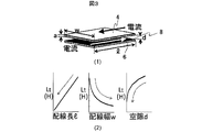
- FIG. 3 is an explanatory diagram showing the relationship between the length, width and thickness of the opposing metal foils on the circuit board constituting the power semiconductor module according to this embodiment, and the inductance.
- inductive power is generated so as to cancel the change in the magnetic flux as the magnetic flux changes due to the current.
- self-inductance The ease with which self-induction occurs is called self-inductance and can be calculated by the following equation.
- inductive power is generated along with the change in magnetic flux due to the current.
- the ease of induction is called mutual inductance, and can be calculated by the following equation.
- M ⁇ o ⁇ l / 2 ⁇ [ln ⁇ 2l / f (w, d) ⁇ ⁇ 1] (H)
- d indicates the thickness of the insulating material.
- the current paths are opposed to cancel generated magnetic flux to reduce inductance.
- the magnetic flux generated in the metal foil 4 and a part of the magnetic flux generated in the metal foil 6 are offset.
- the inductance generated by the metal foil 4 and the metal foil 6 can be obtained by the following equation.
- FIG. 3 shows a characteristic in which the value of the inductance L (t) generated by the metal foil 4 and the metal foil 6 in the circuit board varies depending on the wiring length (l), the wiring width (w), and the air gap (d). Yes.
- the length (l) of the metal foil is shortened, the width (w) is widened, the thickness of the insulating material is narrowed, and the distance (d) between the metal foils is shortened to increase the magnetic flux canceling action.
- the inductance of the circuit board can be reduced, and the energy stored in the inductance is reduced, so that the effect of suppressing the jumping voltage is obtained.
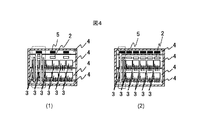
- FIG. 4 is a diagram showing the positional relationship between a number of semiconductor elements mounted in parallel and the positive terminal and the negative terminal according to this embodiment.
- two or more pairs of terminals 2 and 5 to be bonded to the metal foil 4 are provided in the long side direction of the circuit board.
- the terminals 2 and 2 5 By repeating the same pattern on the circuit board, the terminals 2 and 2 5, the size of the current loop formed through the semiconductor element 3 and the metal foils 4 and 6 can be made uniform.
- the terminals 2 and 5 are arranged at corresponding positions between the semiconductor elements 3 placed on the metal foil 4. At that time, as indicated by a dotted line in FIG. 4A, the same pattern is repeated on the circuit board, whereby the size of the current loop formed on the circuit board can be made uniform. Further, as shown in FIG. 4B, the terminals 2 and 5 may be arranged for each semiconductor element 3 placed on the metal foil 4. At that time, as shown in FIG. 4 (1), as shown by a dotted line in FIG. 4 (2), by repeating the same pattern on the circuit board 1, the size of the current loop formed on the circuit board is made uniform. Can be
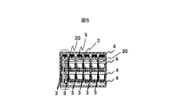
- FIG. 5 is a diagram showing the shape of the metal foil arrangement pattern on the circuit board according to this embodiment.
- slits 30 are provided in the short side direction of the metal foil 4 for each of the positive electrode side terminal 2 and the negative electrode side terminal 5, and the shape of the current path flowing on each metal foil divided by the slit 30 is uniform.
- the shape of the current flowing from the positive electrode side terminal 2 onto the metal foil is designated.
- the inductance is slightly increased because the width of the current path is narrowed, the size of the current loop can be made uniform and the size of the current loop can be arbitrarily changed by the partitioning shape by the slit 30. It becomes possible.
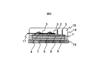
- FIG. 6 is a diagram showing an overall configuration of the power semiconductor module according to the present embodiment.
- the power semiconductor module includes a circuit board 1, a semiconductor element 3 placed on the circuit board 1, a positive terminal 2, a negative terminal 5, metal foils 4, 6, 7, an insulating material 8, 9, a module case 14, a heat dissipation base 15 fixed to the metal foil 7, an insulating gel 16, and an exhaust heat bus bar 17 whose surface is insulated.
- the exhaust heat bus bar 17 radiates heat from the surface of the semiconductor element 3 to reduce heat generation due to thermal resistance that increases with an increase in the number of laminated metal foils on the circuit board 1.
- the exhaust heat bus bar 17 is not linear, and may have a shape that increases the surface area, such as corrugated or perforated. Moreover, the structure which encloses a refrigerant
- coolant may be sufficient. At that time, the vaporized refrigerant may be cooled on the surface of the bus bar outside the semiconductor module and liquefied again.
- the exhaust heat bus bar 17 and the semiconductor element 3 are connected to exhaust heat.
- the exhaust heat bus bar 17 not only directly cools the semiconductor element 3, but also insulates above the semiconductor element.
- the structure which cools the semiconductor element 3 by cooling the gel 16 may be sufficient.
- attaches inside the module case 14 and cools the whole semiconductor module from the module case 14 may be sufficient.
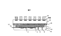
- FIG. 7 is a diagram showing a power conversion device provided with a cooling mechanism in the power semiconductor module according to the present embodiment.
- the configuration example shown in FIG. 7 is a power conversion device in which cooling fins 18 are attached to the heat dissipation base 15 of the power semiconductor module shown in FIG.
- a heat pipe-like radiator 19 is attached to the cooling fin 18, and the refrigerant is sealed inside the radiator 19, thereby cooling the semiconductor module due to a change in the state of the refrigerant.
- the refrigerant in the heat pipe is warmed and raised by the cooling fins 18 and cooled by the outside air and lowered.
- the heat pipe-shaped radiator 19 may have a configuration in which the cooling performance is improved by providing irregularities.
- the cooling pipe 18 is provided with a heat pipe-shaped radiator 19 encapsulating a refrigerant, but the cooling fin 18 itself may be immersed in the refrigerant. At that time, the refrigerant heated and vaporized by the fins can be liquefied on the surface of the case containing the fins and the refrigerant, and the cooling performance can be improved by cooling the fins again.
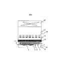
- FIG. 8 is a view showing a power conversion device provided with another cooling mechanism in the power semiconductor module according to the present embodiment.
- the cooling fin 18 of the power conversion device shown in FIG. 7 is connected to the external cooler 20 (with a cooling function independent of itself as a cooler) via the connection pipe 21. It is the attached power converter.
- the cooling performance of the semiconductor module is improved by directly connecting the cooling fins 18 and the external cooler 20, and the heat of the circuit board 1 in which the metal foil and the insulating material are laminated is removed. be able to.
- the heat pipe radiator 9 may not be an essential component.
- connection pipes 21 may be provided, and the shape is not limited to a cylindrical shape, and a configuration in which unevenness is provided to improve cooling performance may be used.
- the semiconductor module may be cooled by changing the state of the refrigerant by including not only air but also a refrigerant in the connection pipe 21, and in this case, the vaporized refrigerant is cooled on the surface of the connection pipe and then again. Cooling is realized by liquefying. Further, even if the connection pipe 21 is not provided between the cooling fin 18 and the external cooler 20, the cooling fin 18 is covered without covering the space between the two without leaking the cooling function of the external cooler 20 to the outside. It may be a structure to convey.
- a module having a 2 in 1 configuration (a configuration including an upper and lower arm series circuit in one module) as illustrated in FIG. 1 has been described as an example.
- a module having a 1 in 1 configuration in which a single switch unit is mounted, or a module having a 6 in 1 configuration in which six switch units are mounted in one module may be used.
- the present invention is not limited to the above-described embodiments, and it goes without saying that various configuration examples belonging to the scope of the technical idea of the present invention are included.
Landscapes
- Inverter Devices (AREA)
Abstract
パワー半導体モジュールのインダクタンスを低減し、且つ多数並列に実装した半導体素子間の電流バランスを改善すること。 複数の金属層間4,6に絶縁層8を介在させて積層構造とした矩形状の回路基板1と、正極側端子2と、負極側端子5と、上層金属層に載置された半導体素子3と、を備え、上層金属層4は半導体素子3の外に正極側端子2と下層金属層6と電気的接続され、下層金属層6は負極側端子5と電気的接続され、正極側端子2と負極側端子5とは近接した位置で対として配置され、正極側端子2及び負極側端子5と半導体素子3とを通る電流経路は、回路基板1の短辺方向に沿って形成され、正極側端子2と負極側端子5の対が回路基板1の長辺方向に沿って複数設置されること。半導体素子3は上層金属層4の短辺方向に沿って複数並列して配置されること。また、複数の半導体素子3に流れる電流通路は互いに略同一の電流通路長さを有すること。
Description
本発明は、パワー半導体モジュール及びこれを用いた電力変換装置に係わり、特に、多層の回路基板に適用したパワー半導体モジュールの構成に関する。
一般に、電流経路を対向させることによって、発生する磁束を相殺させ、回路基板のインダクタンスを低減させることは、従来から知られている。そして、回路基板を多層化し、表層配線と内層配線の電流を対向させて、回路基板のインダクタンスを低減する従来技術は、例えば特許文献1に開示されている。この特許文献1に記載された半導体装置では、グランドと電源の2層の配線が積層された配線基板において、電源(+電流)とグランドライン(-電流)とに対向電流を流すことでインダクタンスを低減する構成が用いられている。
また、特許文献2に記載されたパワー半導体モジュールには、多層の配線基板において内層配線をグランド配線とする構成が示されている(特許文献2の図6を参照)。
ところで、電力変換器で発生するスイッチングに伴う電力損失を低減するには、絶縁ゲートバイポーラトランジスタ(IGBT)におけるスイッチングの高速化による高速駆動と、半導体モジュールへのワイドギャップ半導体素子(例.IGBTとショットキーバリアダイオード)の搭載によるリカバリー電流の減少と、が有効である。
ここで、半導体素子の高速駆動時には高周波の電流振動が発生するが、これに対してはインダクタンスを低減することによって、電流振動を抑制することができる。また、ワイドギャップ半導体素子を搭載した大容量半導体モジュールを形成するには、当該ワイドギャップ半導体素子(SiC、GaN)が歩留まりの点から小容量のものしか製造でき難い実情からすると、ワイドギャップ半導体素子を多数並列に実装することが必要である。
その際、搭載すべき半導体素子の数を一定とすると、一の回路基板に比較的少ない数の半導体素子を搭載した場合には回路基板の数を増加せざると得ず、この回路基板の数の増加は装置の大型化や駆動信号のばらつきにつながるおそれがある。そのため、回路基板あたりの半導体素子を多数搭載する(すなわち、回路基板の数を少なくする)ことの方が望ましい。
ところで、上記の特許文献1には、多層配線基板の積層構造において、電源ラインとグランドライン間の電流の大きさを略等しくし且つ電流の向きを逆とすることでインダクタンスの低減を図ることが開示されてはいるが、多層の配線基板上における半導体素子と接続端子との位置関係については特段の記載はない。特に、半導体素子の多並列実装時においては、配線基板のインダクタンスが低減する一方で、半導体素子間のインダクタンスのばらつきが大きくなり、わずかなインダクタンスばらつきが各半導体素子の負荷、発熱のばらつきに発展するおそれがある。また、半導体素子と接続端子の位置次第によっては、形成される電流ループが大きくなり、相殺する磁束数が少なくなってインダクタンスの低減にむすびつかないこととなる。
また、上記の特許文献2に示す構成においては、電源パタンから半導体素子を経由して形成される電流ループの大きさが不均一であるため、等価的にインダクタンスがばらついて電流ループの電流バランスがくずれることとなり、ループ毎の半導体素子の動作不安定と故障に結び付くこととなる。このように、特許文献2に開示の構成では、低インダクタンス基板において半導体素子を多数並列に実装した場合の課題である、半導体素子間のインダクタンスばらつき、電流アンバランスの影響を受けることとなる。
本発明の目的は、パワー半導体モジュールのインダクタンスを低減でき、且つ、多数並列に実装した半導体素子間の電流バランスを改善するパワー半導体モジュールを提供することにある。
上記課題を解決するために、本発明は主として次のような構成を採用する。
少なくとも2層の絶縁層と3層の金属層を有し、前記金属層間に前記絶縁層を介在させて積層構造とした矩形状の回路基板と、正極電流を流す正極側端子と、負極電流を流す負極側端子と、前記金属層の内で上層の金属層に載置された半導体素子と、を備え、
前記上層金属層は、半導体素子に加えて前記正極側端子と電気的接続され、さらに前記上層金属層の下に配された下層金属層と電気的接続され、前記下層金属層は、前記負極側端子と電気的接続され、前記正極側端子と前記負極側端子とは前記回路基板上で近接した位置で対として配置され、前記正極側端子及び前記負極側端子と前記半導体素子とを通る電流経路は、前記矩形状の回路基板の短辺方向に沿って形成され、前記正極側端子と前記負極側端子の対が、前記矩形状の回路基板の長辺方向に沿って複数設置される構成とする。
少なくとも2層の絶縁層と3層の金属層を有し、前記金属層間に前記絶縁層を介在させて積層構造とした矩形状の回路基板と、正極電流を流す正極側端子と、負極電流を流す負極側端子と、前記金属層の内で上層の金属層に載置された半導体素子と、を備え、
前記上層金属層は、半導体素子に加えて前記正極側端子と電気的接続され、さらに前記上層金属層の下に配された下層金属層と電気的接続され、前記下層金属層は、前記負極側端子と電気的接続され、前記正極側端子と前記負極側端子とは前記回路基板上で近接した位置で対として配置され、前記正極側端子及び前記負極側端子と前記半導体素子とを通る電流経路は、前記矩形状の回路基板の短辺方向に沿って形成され、前記正極側端子と前記負極側端子の対が、前記矩形状の回路基板の長辺方向に沿って複数設置される構成とする。
また、前記パワー半導体モジュールにおいて、前記半導体素子はスイッチング素子とダイオードからなり、前記半導体素子は前記上層金属層の短辺方向に沿って複数並列して配置されること。さらに、前記複数設置のそれぞれの対における前記正極側端子と前記負極側端子から、当該端子に対応してそれぞれ配置された前記半導体素子に流れる複数の電流通路は、互いに略同一の電流通路長さを有すること。
本発明によれば、パワー半導体モジュールにおける低インダクタンス化と多数並列に実装した半導体素子間の電流バランスの改善を両立することができる。これによって、半導体素子に流れる電流振動を抑制することができるとともに、パワー半導体モジュールのスイッチングに伴う電力損失を低減することができる。
また、回路基板あたりの半導体素子の搭載数を増加することができ、小型かつ大容量の半導体モジュールを構成することができる。
本発明の実施形態に係るパワー半導体モジュールについて、図面を参照しながら以下説明する。図1は本発明の実施形態に係るパワー半導体モジュールを構成する多数並列実装された半導体素子、正極側端子、負極側端子、回路基板の配置構成と、電流の流れと、を示す図である。図1において、1は回路基板、2は正極側端子、3は半導体素子、4は半導体素子及び正極側端子と電気的接続する金属箔、5は負極側端子、6は金属箔4及び負極側端子と電気的接続する金属箔、7は回路基板と放熱ベース15を接続する金属箔、8は金属箔4と金属箔6を絶縁する絶縁材、9は金属箔6と金属箔7を絶縁する絶縁材、をそれぞれ表す。
図1において、回路基板1は、半導体素子3を戴置する金属箔4と、金属箔4と電気的に接続する金属箔6と、金属箔4と金属箔6を積層する絶縁材8と、放熱板15(図6を参照)と接続する金属箔7と、金属箔6と金属箔7を積層する絶縁材9と、から成り立っていて、これらの各構成要素を積層接着させたものである。図1(1)には、回路基板1上の各構成要素の載置状態を平面図及び側面図として示し、図1(2)には、回路基板1上の各構成要素の載置状態を分解図として示している。
本実施形態に係るパワー半導体モジュールは、半導体素子3と、回路基板1と、正極電流を供給する正極側端子2と、負極電流を供給する負極側端子5と、放熱ベース15(図6を参照)と、を基本的な構成としている。正極側端子2と負極側端子5とは、金属箔4,6上においてそれぞれ近接して配置され、回路基板1の長辺方向に2対以上設けられている(図示例では3対の端子2,5が長辺方向に並列実装されている)。図1において、半導体素子3は、IGBTとダイオードから成り立って1つのアーム(スイッチ部)を形成しており、図1では上下に半導体素子3,3が図示されていて、いわゆる上下アーム直列回路が図示されている。そして、図示例ではこの上下アーム直列回路が6個並列に実装されている。
正極側端子2と負極側端子5との間に流れる電流は、回路基板1内において回路基板1の短辺方向の流れである。ここで、端子2,5間を流れる電流は、例えば、上アームのIGBTがオフ状態で且つ下アームのIGBTがオンになった時に流れるリカバリー電流である。そして、下アームには、インバータ回路として正常動作時の電流がリカバリー電流に重畳されている。
ここで、後述する図4(1)に示すように、正極側及び負極側端子2,5は、金属箔4上に戴置された半導体素子3の間に対応する位置に配置してもよく、また、図4(2)に示すように、各半導体素子3に対向する位置に配置してもよい。また、正極側及び負極側端子2,5の設置位置は回路基板1の基板端部に限定されず、回路基板1の長辺方向であればどこで並列実装してもよい。また、半導体素子3と金属箔4の接続については、ワイヤボンドだけでなく、リボンボンドやフリップチップ実装によってもよい。
図2は、本実施形態に係るパワー半導体モジュールを構成する多数並列実装された半導体素子と、正極側端子及び負極側端子と、における等価回路を示す図であり、図1に示す構成に対応する等価回路である。半導体素子は、そのスイッチのオフ時に、半導体素子の接合容量と寄生のインダクタンスにより、高周波の共振電流が発生し、この共振電流により電圧も振動する。ここで、高周波とは、パワー半導体モジュールを用いた電力変換器の出力周波数の最大値より100倍以上大きい周波数のことである。
この共振電流はスイッチの遮断速度が大きいほど顕著になる。このため、シリコンを使用した半導体素子よりも、シリコンカーバイドやガリウムナイトライドのようなワイドギャップ半導体の方が電流の振動は大きくなり、電磁ノイズを引き起こすおそれがある。
そこで、電流振動の抑制には寄生インダクタンスの低減が有効であるが、図2に示すように、特に、一つの基板に半導体素子3を多数並列実装する場合においては(大容量の半導体モジュールを形成するために)、基板に戴置される半導体素子3間のインダクタンスのばらつきが、各半導体素子のスイッチのタイミングに影響を及ぼすという不都合が生じる。
本発明の実施形態によれば、金属箔4と金属箔6において、回路基板1の短辺方向(図1の図示例で紙面上下方向)に電流を流すことによって、回路基板1の長辺方向に電流を流した場合と対比すると、電流経路の長さが短く且つ電流経路の幅が広くなるため、金属箔4,6からなる導体に電流が流れる際に発生するインダクタンスを低減することができる(その理由は後述の図3で説明する)。
さらに、回路基板1上に電流を流す金属箔4と金属箔6が絶縁材8を介した積層構造となっているために、積層された金属箔4,6の表面のうち、他方の金属箔と対向する面において電流が集中(積層する金属箔では対向する金属面の側に電流が集中)し、対向して流れる電流の空隙が狭くなって、発生する磁束をより多く相殺することで、回路基板のインダクタンスを低減することができる(その理由は後述の図3で説明する)。
また、正極側端子2と負極側端子5の対を2つ以上設けることで(図1の図示例で3つ)、端子2,5から半導体素子3を経て形成される電流ループの大きさが均一化され、半導体素子3の間で発生するインダクタンスのばらつきを低減する効果がある。換言すると、半導体素子3を回路基板1に多数並列実装する場合に、図4に示すように、並列実装した半導体素子3毎に、又は2つの半導体素子毎に、端子2,5を設けることによって、それぞれの端子2,5からみた半導体素子の電流ループは、その大きさが均一化されていることになる(図1の例で、例えば左端の一対の端子のみで、6個の上下アームのリカバリー電流通路を形成するものと対比すると、電流ループの大きさが均一化される)。
以上説明したように、本実施形態によれば、低インダクタンス化と半導体素子間インダクタンスばらつき(電流アンバランスに結び付く)の低減を両立でき、スイッチングに伴う電力損失の低減、インダクタンス低減による共振周波数のずれがもたらすノイズの低減、跳ね上がり電圧の抑制だけでなく、各半導体素子のスイッチばらつきの抑制が可能となり、基板あたりに実装できる半導体素子の数を増加でき、かつ電力変換器を安全に駆動することができる。すなわち、電力変換器の安全駆動の意味は、各半導体素子への電流ループが不均一になると、一の半導体素子への過度のリカバリー電流の偏りによる当該半導体素子の故障確率が高くなることに比べて、多数並列実装時のそれぞれの半導体素子の電流ループを均一にすることで故障確率を低くして、長持ちさせることである。
特に、SiC(炭化ケイ素)やGaN(窒化ガリウム)のようなデバイスを用いて大容量半導体モジュールを構成する場合、小容量のチップを多並列で基板に実装する必要があるが、半導体素子間のインダクタンスのばらつき低減によって半導体素子毎の負荷や発熱の差を抑制できる。また、高速駆動のデバイスは、従来用いられていたSiよりも高速で遮断可能であるため、高速駆動に伴うdV/dtの増大によって電流の振動及び跳ね上がり電圧の増大が課題となっていたので、半導体素子間のインダクタンスのばらつき低減の効果は大きい。
図3は本実施形態に係るパワー半導体モジュールを構成する回路基板における対向する金属箔の長さ、幅、厚みと、インダクタンスとの関係を示す説明図である。図3において、金属箔4に電流が流れた場合、電流による磁束の変化に伴い、磁束の変化を打ち消すように誘導電力が発生する。自己誘導の起こしやすさを自己インダクタンスと呼び、次式にて求めることができる。
L=μo×l/2π[ln{2l/(a+w)}+1/2] (H)
ここで、μoは金属箔の透磁率、lは金属箔長、aは金属箔厚み、wは金属箔幅を示す。
ここで、μoは金属箔の透磁率、lは金属箔長、aは金属箔厚み、wは金属箔幅を示す。
また、金属箔4と対向する金属箔6に電流が流れた場合、電流による磁束の変化に伴い、誘導電力が発生する。誘導の起こしやすさを相互インダクタンスと呼び、次式にて求めることができる。
M=μo×l/2π[ln{2l/f(w,d)}-1] (H)
ここで、dは絶縁材の厚みを示す。
ここで、dは絶縁材の厚みを示す。
一般に、電流経路を対向させることによって、発生する磁束を相殺してインダクタンスを低減することは、従来から知られている。ここでは、金属箔4の電流経路と金属箔6の電流経路を対向させることで、金属箔4で発生する磁束と金属箔6で発生する磁束の一部が相殺される。金属箔4と金属箔6によって発生するインダクタンスは、次式にて求めることができる。
L(t)=2L-2M
図3には、回路基板における金属箔4と金属箔6によって発生するインダクタンスL(t)の値が、配線長(l)、配線幅(w)、空隙(d)によって変化する特性を表している。
図3には、回路基板における金属箔4と金属箔6によって発生するインダクタンスL(t)の値が、配線長(l)、配線幅(w)、空隙(d)によって変化する特性を表している。
図示の説明によると、金属箔の長さ(l)を短く、その幅(w)を広く、絶縁材の厚みを狭め金属箔間の距離(d)を短くして磁束相殺作用を大きくすることによって、回路基板のインダクタンスを低減することができ、インダクタンスに蓄えられるエネルギーが小さくなるため、跳ね上がり電圧抑制の効果が得られる。
図4は本実施形態に関する多数並列実装された半導体素子と、正極側端子及び負極側端子と、の位置関係を示す図である。図4に示す回路基板では、金属箔4と接着する端子2,5の対が回路基板の長辺方向に2つ以上設けられており、回路基板上に同じパターンを繰り返すことで、端子2,5から半導体素子3と金属箔4,6を経て形成される電流ループの大きさを均一化できる。
ここで、図4(1)に示すように、端子2,5は金属箔4上に戴置された半導体素子3の間の対応位置に配置する構成となっている。その際、図4(1)において点線で示すように、回路基板上に同じパターンを繰り返すことで、回路基板上に形成される電流ループの大きさを均一化できる。また、図4(2)に示すように、端子2,5は金属箔4上に戴置された半導体素子3毎に配置する構成であっても良い。その際、図4(1)と同様に、図4(2)において点線で示すように、回路基板1上に同じパターンを繰り返すことで、回路基板上に形成される電流ループの大きさを均一化できる。
このように、電流ループを複数設け且つ電流ループの大きさを均一化することで、回路基板1のインダクタンスと半導体素子3間のインダクタンスばらつきの低減を両立できる。これにより、跳ね上がり電圧による素子破壊の防止、半導体素子間の発熱や駆動速度のばらつき低減を実現でき、回路基板あたりに搭載できる半導体素子数を増加することができる。
図5は本実施形態に関する回路基板における金属箔の配置パターンの形状を示す図である。図5に示す構成例は、正極側端子2と負極側端子5毎に金属箔4の短辺方向にスリット30を設け、スリット30で区分けされた各金属箔上を流れる電流経路の形状を均一化させ、正極側端子2から金属箔上に流れる電流の形状を指定するものである。この構成例においては、電流経路の幅が狭まるためインダクタンスがやや増加するものの、スリット30による区分け形状により、電流ループの大きさを均一にするとともに、電流ループの大きさを任意に変更することが可能となる。
図6は本実施形態に係るパワー半導体モジュールの全体構成を示す図である。図6に示すように、パワー半導体モジュールは、回路基板1、回路基板1に戴置された半導体素子3、正極側端子2、負極側端子5、金属箔4,6,7、絶縁材8,9、モジュールケース14、金属箔7に固設された放熱ベース15、絶縁用ゲル16、表面に絶縁処理を施した排熱用バスバー17、から構成される。図6において、回路基板1の金属箔の積層数増加ともに増大する熱抵抗による発熱を低減するために、排熱用バスバー17は半導体素子3の表面から外部に放熱するものである。
ここで、排熱用バスバー17は直線状でなくて、波形や穴あき等のように表面積を増やす形状であってもよい。また、排熱用バスバー17内に冷媒を封入し、冷媒の状態変化により冷却する構成であってもよい。その際、気化した冷媒は、半導体モジュール外部のバスバー表面で冷却し再度液化してもよい。
図6においては、排熱用バスバー17と半導体素子3を接続し排熱させる構成としたが、排熱用バスバー17は、半導体素子3を直接冷却するだけでなく、半導体素子の上方で絶縁用ゲル16を冷却することで半導体素子3を冷却する構成であってもよい。また、モジュールケース14の内部に接着し、モジュールケース14から半導体モジュール全体を冷却する構成であってもよい。
図7は本実施形態に係るパワー半導体モジュールに冷却機構を備えた電力変換装置を示す図である。図7に示す構成例は、図6に示すパワー半導体モジュールの放熱ベース15に冷却用フィン18を取り付けた電力変換装置である。図7の構成例では、冷却用フィン18にヒートパイプ状の放熱器19を取り付け、放熱器19の内部に冷媒を封入することで、冷媒の状態変化により半導体モジュールを冷却するものである。ヒートパイプ内の冷媒は、冷却用フィン18で暖められて上昇し、外気で冷却されて下降する。この冷却によって、金属箔と絶縁材を積層させた構成である回路基板1の発熱を低減することができる。また、ヒートパイプ状の放熱器19は、凹凸を設けて冷却性能を向上させた構成であっても良い。
図7においては、冷却用フィン18に対して、冷媒を封入したヒートパイプ状放熱器19を設ける構成としたが、冷却用フィン18自体を冷媒に浸ける構成であっても良い。その際、フィンによって暖められ気化した冷媒は、フィンと冷媒を収めるケースの表面で液化し、再度フィンを冷却することで冷却性能を向上させることができる。
図8は本実施形態に係るパワー半導体モジュールに他の冷却機構を備えた電力変換装置を示す図である。図8に示す構成例は、図7に示す電力変換装置の冷却用フィン18を接続パイプ21を介して外部冷却器20(冷却器としてそれ自体で独立した冷却機能を有したものである)を取り付けた電力変換装置である。図8の構成例では、冷却用フィン18と外部冷却器20を直接接続することによって、半導体モジュールの冷却性能を向上させ、金属箔と絶縁材を積層させた回路基板1の熱を除熱させることができる。なお、図8において、ヒートパイプ状放熱器9は必須の構成要素でなくてもよい。
ここで、接続パイプ21は一つではなく複数設ける構成であってもよく、さらに、その形状は円筒状に限らず、凹凸を設け冷却性能を向上させた構成であっても良い。また、接続パイプ21内に空気だけでなく冷媒を含ませることによって、冷媒の状態変化で半導体モジュールを冷却する構成であってもよく、その際、気化した冷媒は、接続パイプ表面で冷却し再度液化することで冷却を実現する。さらに、冷却用フィン18と外部冷却器20との間に、接続パイプ21を設けなくても、両者間の空間を覆って外部冷却器20による冷却機能を外部に漏らすこと無く冷却用フィン18に伝える構造であってもよい。
以上のように、本発明の実施形態では、図1に示すような、2in1の構成のモジュール(1つのモジュール内に上下アーム直列回路を含む構成)を例に説明したが、1モジュール内に1個のスイッチ部を搭載した1in1の構成のモジュールや、1モジュール内に6個のスイッチ部を搭載した6in1の構成のモジュールであっても良い。さらに、本発明は、上述した実施形態に限定されるものではなく、本発明の技術的思想の範囲内に属する種々の構成例が含まれることは言うまでもない。
1 回路基板
2 正極側端子
3 半導体素子
4 半導体素子及び正極側端子と電気的接続する金属箔
5 負極側端子
6 金属箔4及び負極側端子と電気的接続する金属箔
7 回路基板と放熱ベースを接続する金属箔
8 金属箔4と金属箔6を絶縁する絶縁材
9 金属箔6と金属箔7を絶縁する絶縁材
14 モジュールケース
15 放熱ベース
16 絶縁用ゲル
17 排熱用バスバー
18 冷却用フィン
19 ヒートパイプ状放熱器
20 外部冷却器
21 冷却用フィンと外部冷却器の接続パイプ
30 スリット
2 正極側端子
3 半導体素子
4 半導体素子及び正極側端子と電気的接続する金属箔
5 負極側端子
6 金属箔4及び負極側端子と電気的接続する金属箔
7 回路基板と放熱ベースを接続する金属箔
8 金属箔4と金属箔6を絶縁する絶縁材
9 金属箔6と金属箔7を絶縁する絶縁材
14 モジュールケース
15 放熱ベース
16 絶縁用ゲル
17 排熱用バスバー
18 冷却用フィン
19 ヒートパイプ状放熱器
20 外部冷却器
21 冷却用フィンと外部冷却器の接続パイプ
30 スリット
Claims (12)
- 少なくとも2層の絶縁層と3層の金属層を有し、前記金属層間に前記絶縁層を介在させて積層構造とした矩形状の回路基板と、正極電流を流す正極側端子と、負極電流を流す負極側端子と、前記金属層の内で上層の金属層に載置された半導体素子と、を備え、
前記上層金属層は、半導体素子に加えて前記正極側端子と電気的接続され、さらに前記上層金属層の下に配された下層金属層と電気的接続され、
前記下層金属層は、前記負極側端子と電気的接続され、
前記正極側端子と前記負極側端子とは前記回路基板上で近接した位置で対として配置され、
前記正極側端子及び前記負極側端子と前記半導体素子とを通る電流経路は、前記矩形状の回路基板の短辺方向に沿って形成され、
前記正極側端子と前記負極側端子の対が、前記矩形状の回路基板の長辺方向に沿って複数設置される
ことを特徴とするパワー半導体モジュール。 - 請求項1において、
前記半導体素子はスイッチング素子とダイオードからなり、前記半導体素子は前記上層金属層の短辺方向に沿って複数並列して配置されることを特徴とするパワー半導体モジュール。 - 請求項1又は2において、
前記複数設置のそれぞれの対における前記正極側端子と前記負極側端子から、当該端子に対応してそれぞれ配置された前記半導体素子に流れる複数の電流通路は、互いに略同一の電流通路長さを有する
ことを特徴とするパワー半導体モジュール。 - 請求項1、2または3において、
前記半導体素子は、シリコンカーバイド又はガリウムナイトライドを含むワイドギャップ半導体であり、シリコンよりも高速に遮断可能なデバイスであることを特徴とするパワー半導体モジュール。 - 請求項1ないし4のいずれか1つの請求項において、
前記矩形状の回路基板上で、前記正極側端子と前記負極側端子と前記半導体素子の配置は、前記回路基板の短辺方向に沿って配置され、当該配置は同一パターンの繰り返しで複数並列実装されていることを特徴とするパワー半導体モジュール。 - 請求項1ないし5のいずれか1つの請求項において、
前記正極側端子及び前記負極側端子毎に前記上層金属層の短辺方向にスリットを設け、前記スリットで区切られたそれぞれの金属層を流れる電流経路を均一化させることを特徴とするパワー半導体モジュール。 - 請求項1ないし6のいずれか1つの請求項において、
前記正極側端子と前記負極側端子は、前記上層金属層の短辺方向に並列配置された半導体素子同士の中間位置に対応する位置に設けることを特徴とするパワー半導体モジュール。 - 請求項1ないし6のいずれか1つの請求項において、
前記正極側端子と前記負極側端子は、前記上層金属層の短辺方向に並列配置された半導体素子の各位置に対応する位置に設けることを特徴とするパワー半導体モジュール。 - 請求項1ないし6のいずれか1つの請求項において、
前記半導体素子を載置した前記上層金属層とは逆側の最下層の金属層に放熱ベースを取り付け、
前記上層金属層に載置された複数の半導体素子に接続された高熱伝導導体の排熱用バスバーを設ける
ことを特徴とするパワー半導体モジュール。 - 複数の金属層間に絶縁層を介在させて積層構造とした矩形状の回路基板と、正極電流を流す正極側端子と、負極電流を流す負極側端子と、前記金属層の内で上層の金属層に載置された半導体素子と、を備え、前記上層金属層は、半導体素子に加えて前記正極側端子と電気的接続され、さらに前記上層金属層の下に配された下層金属層と電気的接続され、前記下層金属層は、前記負極側端子と電気的接続され、前記正極側端子と前記負極側端子とは前記回路基板上で近接した位置で対として配置され、前記正極側端子及び前記負極側端子と前記半導体素子とを通る電流経路は、前記矩形状の回路基板の短辺方向に沿って形成され、前記正極側端子と前記負極側端子の対が、前記矩形状の回路基板の長辺方向に沿って複数設置され、前記半導体素子を載置した前記上層金属層とは逆側の最下層の金属層に放熱ベースを取り付けたパワー半導体モジュールを用い、
前記パワー半導体モジュールの前記放熱ベースに冷却用フィンを取り付ける
ことを特徴とする電力変換装置。 - 請求項10において、
前記冷却用フィンに対して、冷媒を封入したヒートパイプ状放熱器を設置することを特徴とする電力変換装置。 - 請求項10において、
前記冷却用フィンに対して、独自に冷却機能を有した外部の冷却器を直接接続することを特徴とする電力変換装置。
Priority Applications (3)
| Application Number | Priority Date | Filing Date | Title |
|---|---|---|---|
| JP2014551810A JP6155282B2 (ja) | 2012-12-13 | 2012-12-13 | パワー半導体モジュール及びこれを用いた電力変換装置 |
| PCT/JP2012/082403 WO2014091608A1 (ja) | 2012-12-13 | 2012-12-13 | パワー半導体モジュール及びこれを用いた電力変換装置 |
| TW102136770A TW201436154A (zh) | 2012-12-13 | 2013-10-11 | 功率半導體模組及使用彼之電力變換裝置 |
Applications Claiming Priority (1)
| Application Number | Priority Date | Filing Date | Title |
|---|---|---|---|
| PCT/JP2012/082403 WO2014091608A1 (ja) | 2012-12-13 | 2012-12-13 | パワー半導体モジュール及びこれを用いた電力変換装置 |
Publications (1)
| Publication Number | Publication Date |
|---|---|
| WO2014091608A1 true WO2014091608A1 (ja) | 2014-06-19 |
Family
ID=50933927
Family Applications (1)
| Application Number | Title | Priority Date | Filing Date |
|---|---|---|---|
| PCT/JP2012/082403 Ceased WO2014091608A1 (ja) | 2012-12-13 | 2012-12-13 | パワー半導体モジュール及びこれを用いた電力変換装置 |
Country Status (3)
| Country | Link |
|---|---|
| JP (1) | JP6155282B2 (ja) |
| TW (1) | TW201436154A (ja) |
| WO (1) | WO2014091608A1 (ja) |
Cited By (10)
| Publication number | Priority date | Publication date | Assignee | Title |
|---|---|---|---|---|
| WO2016084241A1 (ja) * | 2014-11-28 | 2016-06-02 | 日産自動車株式会社 | ハーフブリッジパワー半導体モジュール及びその製造方法 |
| WO2017090281A1 (ja) * | 2015-11-25 | 2017-06-01 | シャープ株式会社 | モジュール基板 |
| CN108231751A (zh) * | 2016-12-15 | 2018-06-29 | 英飞凌科技股份有限公司 | 用于功率电路的平行板波导结构 |
| CN110034100A (zh) * | 2017-11-15 | 2019-07-19 | 夏普株式会社 | 功率半导体组件及电子设备 |
| US10410952B2 (en) | 2016-12-15 | 2019-09-10 | Infineon Technologies Ag | Power semiconductor packages having a substrate with two or more metal layers and one or more polymer-based insulating layers for separating the metal layers |
| US10811329B2 (en) | 2015-02-17 | 2020-10-20 | Koninklijke Philips N.V. | Ceramic substrate and method for producing a ceramic substrate |
| WO2021117227A1 (ja) * | 2019-12-13 | 2021-06-17 | 三菱電機株式会社 | 半導体装置、半導体システム、移動体、及び半導体装置の製造方法 |
| WO2021225072A1 (ja) * | 2020-05-08 | 2021-11-11 | 株式会社日立製作所 | 電力変換装置 |
| CN114365280A (zh) * | 2019-09-04 | 2022-04-15 | 株式会社电装 | 功率模块 |
| CN115547954A (zh) * | 2022-10-20 | 2022-12-30 | 臻驱科技(上海)有限公司 | 一种带镂空结构的双面散热的功率半导体模块 |
Citations (5)
| Publication number | Priority date | Publication date | Assignee | Title |
|---|---|---|---|---|
| JPH11354955A (ja) * | 1998-06-11 | 1999-12-24 | Mitsubishi Electric Corp | 電子機器の冷却構造 |
| JP2002373971A (ja) * | 2001-03-30 | 2002-12-26 | Hitachi Ltd | 半導体装置 |
| JP2010087400A (ja) * | 2008-10-02 | 2010-04-15 | Mitsubishi Electric Corp | 半導体装置 |
| JP2011222707A (ja) * | 2010-04-08 | 2011-11-04 | Mitsubishi Electric Corp | 電力用半導体装置 |
| WO2013018811A1 (ja) * | 2011-08-01 | 2013-02-07 | 富士電機株式会社 | パワー半導体モジュール |
Family Cites Families (6)
| Publication number | Priority date | Publication date | Assignee | Title |
|---|---|---|---|---|
| JP3521757B2 (ja) * | 1998-09-08 | 2004-04-19 | 株式会社豊田自動織機 | 半導体モジュール電極構造 |
| JP2004186504A (ja) * | 2002-12-04 | 2004-07-02 | Hitachi Unisia Automotive Ltd | 半導体装置 |
| JP4479365B2 (ja) * | 2004-06-14 | 2010-06-09 | 日産自動車株式会社 | 半導体装置 |
| JP4946845B2 (ja) * | 2007-12-13 | 2012-06-06 | 株式会社豊田自動織機 | 半導体装置 |
| JP2011036015A (ja) * | 2009-07-31 | 2011-02-17 | Daikin Industries Ltd | 電力変換装置 |
| FR2974969B1 (fr) * | 2011-05-03 | 2014-03-14 | Alstom Transport Sa | Dispositif d'interconnexion electrique d'au moins un composant electronique avec une alimentation electrique comprenant des moyens de diminution d'une inductance de boucle entre des premiere et deuxieme bornes |
-
2012
- 2012-12-13 JP JP2014551810A patent/JP6155282B2/ja active Active
- 2012-12-13 WO PCT/JP2012/082403 patent/WO2014091608A1/ja not_active Ceased
-
2013
- 2013-10-11 TW TW102136770A patent/TW201436154A/zh unknown
Patent Citations (5)
| Publication number | Priority date | Publication date | Assignee | Title |
|---|---|---|---|---|
| JPH11354955A (ja) * | 1998-06-11 | 1999-12-24 | Mitsubishi Electric Corp | 電子機器の冷却構造 |
| JP2002373971A (ja) * | 2001-03-30 | 2002-12-26 | Hitachi Ltd | 半導体装置 |
| JP2010087400A (ja) * | 2008-10-02 | 2010-04-15 | Mitsubishi Electric Corp | 半導体装置 |
| JP2011222707A (ja) * | 2010-04-08 | 2011-11-04 | Mitsubishi Electric Corp | 電力用半導体装置 |
| WO2013018811A1 (ja) * | 2011-08-01 | 2013-02-07 | 富士電機株式会社 | パワー半導体モジュール |
Cited By (23)
| Publication number | Priority date | Publication date | Assignee | Title |
|---|---|---|---|---|
| US10756057B2 (en) | 2014-11-28 | 2020-08-25 | Nissan Motor Co., Ltd. | Half-bridge power semiconductor module and method of manufacturing same |
| JPWO2016084241A1 (ja) * | 2014-11-28 | 2017-10-26 | 日産自動車株式会社 | ハーフブリッジパワー半導体モジュール及びその製造方法 |
| US20170345792A1 (en) * | 2014-11-28 | 2017-11-30 | Nissan Motor Co., Ltd. | Half-bridge power semiconductor module and method of manufacturing same |
| WO2016084241A1 (ja) * | 2014-11-28 | 2016-06-02 | 日産自動車株式会社 | ハーフブリッジパワー半導体モジュール及びその製造方法 |
| US10811329B2 (en) | 2015-02-17 | 2020-10-20 | Koninklijke Philips N.V. | Ceramic substrate and method for producing a ceramic substrate |
| WO2017090281A1 (ja) * | 2015-11-25 | 2017-06-01 | シャープ株式会社 | モジュール基板 |
| EP3349249A3 (en) * | 2016-12-15 | 2018-09-26 | Infineon Technologies AG | Parallel plate waveguide for power circuits |
| US10410952B2 (en) | 2016-12-15 | 2019-09-10 | Infineon Technologies Ag | Power semiconductor packages having a substrate with two or more metal layers and one or more polymer-based insulating layers for separating the metal layers |
| US10453742B2 (en) | 2016-12-15 | 2019-10-22 | Infineon Technologies Ag | Power semiconductor package having a parallel plate waveguide |
| US10319631B2 (en) | 2016-12-15 | 2019-06-11 | Infineon Technologies Ag | Parallel plate waveguide for power semiconductor package |
| CN108231751A (zh) * | 2016-12-15 | 2018-06-29 | 英飞凌科技股份有限公司 | 用于功率电路的平行板波导结构 |
| CN110034100A (zh) * | 2017-11-15 | 2019-07-19 | 夏普株式会社 | 功率半导体组件及电子设备 |
| US10756011B2 (en) | 2017-11-15 | 2020-08-25 | Sharp Kabushiki Kaisha | Power semiconductor module, electronic device, and method for controlling power semiconductor module |
| CN114365280A (zh) * | 2019-09-04 | 2022-04-15 | 株式会社电装 | 功率模块 |
| CN114365280B (zh) * | 2019-09-04 | 2025-09-02 | 株式会社电装 | 功率模块 |
| JPWO2021117227A1 (ja) * | 2019-12-13 | 2021-06-17 | ||
| WO2021117227A1 (ja) * | 2019-12-13 | 2021-06-17 | 三菱電機株式会社 | 半導体装置、半導体システム、移動体、及び半導体装置の製造方法 |
| JP7199575B2 (ja) | 2019-12-13 | 2023-01-05 | 三菱電機株式会社 | 半導体システム及び移動体 |
| CN114787994A (zh) * | 2019-12-13 | 2022-07-22 | 三菱电机株式会社 | 半导体装置、半导体系统、移动体及半导体装置的制造方法 |
| US12243789B2 (en) | 2019-12-13 | 2025-03-04 | Mitsubishi Electric Corporation | Semiconductor device, semiconductor system, moving body, and method for manufacturing semiconductor device |
| WO2021225072A1 (ja) * | 2020-05-08 | 2021-11-11 | 株式会社日立製作所 | 電力変換装置 |
| CN115398621A (zh) * | 2020-05-08 | 2022-11-25 | 株式会社日立制作所 | 电力转换装置 |
| CN115547954A (zh) * | 2022-10-20 | 2022-12-30 | 臻驱科技(上海)有限公司 | 一种带镂空结构的双面散热的功率半导体模块 |
Also Published As
| Publication number | Publication date |
|---|---|
| JPWO2014091608A1 (ja) | 2017-01-05 |
| JP6155282B2 (ja) | 2017-06-28 |
| TW201436154A (zh) | 2014-09-16 |
Similar Documents
| Publication | Publication Date | Title |
|---|---|---|
| JP6155282B2 (ja) | パワー半導体モジュール及びこれを用いた電力変換装置 | |
| JP6865838B2 (ja) | 半導体モジュール及び電力変換装置 | |
| JP6300978B2 (ja) | 電力用半導体モジュール | |
| JP5798412B2 (ja) | 半導体モジュール | |
| JP6127847B2 (ja) | 電力変換装置 | |
| JP6096614B2 (ja) | パワー半導体モジュールおよびそれを用いた電力変換装置 | |
| TWI698969B (zh) | 功率元件封裝結構 | |
| JP2020064913A (ja) | 半導体装置 | |
| WO2013018343A1 (ja) | 半導体モジュール及びそれを搭載したインバータ | |
| JP2013219290A (ja) | 半導体装置 | |
| JP6604926B2 (ja) | 半導体モジュール | |
| US11923266B2 (en) | Semiconductor module circuit structure | |
| JP2007234690A (ja) | パワー半導体モジュール | |
| JP2012175070A (ja) | 半導体パッケージ | |
| WO2018220721A1 (ja) | 半導体パワーモジュール | |
| JP2023183026A (ja) | 半導体装置 | |
| JP7418255B2 (ja) | 電力変換装置 | |
| CN210516724U (zh) | 一种功率半导体模块和功率半导体器件 | |
| JP6818873B2 (ja) | スイッチング素子駆動ユニット | |
| CN117716489B (zh) | 集成GaN功率模块 | |
| US10530354B2 (en) | Insulated gate semiconductor device and method for manufacturing insulated gate semiconductor device | |
| KR102795539B1 (ko) | 파워모듈 | |
| JP2014072385A (ja) | 半導体装置 | |
| JP2016101071A (ja) | 半導体装置 | |
| JP7535444B2 (ja) | 絶縁基板および電力変換装置 |
Legal Events
| Date | Code | Title | Description |
|---|---|---|---|
| 121 | Ep: the epo has been informed by wipo that ep was designated in this application |
Ref document number: 12889881 Country of ref document: EP Kind code of ref document: A1 |
|
| ENP | Entry into the national phase |
Ref document number: 2014551810 Country of ref document: JP Kind code of ref document: A |
|
| NENP | Non-entry into the national phase |
Ref country code: DE |
|
| 122 | Ep: pct application non-entry in european phase |
Ref document number: 12889881 Country of ref document: EP Kind code of ref document: A1 |