WO2014087752A1 - 弾性波装置の製造方法及び弾性波装置 - Google Patents
弾性波装置の製造方法及び弾性波装置 Download PDFInfo
- Publication number
- WO2014087752A1 WO2014087752A1 PCT/JP2013/078521 JP2013078521W WO2014087752A1 WO 2014087752 A1 WO2014087752 A1 WO 2014087752A1 JP 2013078521 W JP2013078521 W JP 2013078521W WO 2014087752 A1 WO2014087752 A1 WO 2014087752A1
- Authority
- WO
- WIPO (PCT)
- Prior art keywords
- functional element
- support layer
- line
- wave device
- holding member
- Prior art date
- Legal status (The legal status is an assumption and is not a legal conclusion. Google has not performed a legal analysis and makes no representation as to the accuracy of the status listed.)
- Ceased
Links
Images








Classifications
-
- H—ELECTRICITY
- H03—ELECTRONIC CIRCUITRY
- H03H—IMPEDANCE NETWORKS, e.g. RESONANT CIRCUITS; RESONATORS
- H03H3/00—Apparatus or processes specially adapted for the manufacture of impedance networks, resonating circuits, resonators
- H03H3/007—Apparatus or processes specially adapted for the manufacture of impedance networks, resonating circuits, resonators for the manufacture of electromechanical resonators or networks
- H03H3/02—Apparatus or processes specially adapted for the manufacture of impedance networks, resonating circuits, resonators for the manufacture of electromechanical resonators or networks for the manufacture of piezoelectric or electrostrictive resonators or networks
-
- H—ELECTRICITY
- H03—ELECTRONIC CIRCUITRY
- H03H—IMPEDANCE NETWORKS, e.g. RESONANT CIRCUITS; RESONATORS
- H03H3/00—Apparatus or processes specially adapted for the manufacture of impedance networks, resonating circuits, resonators
- H03H3/007—Apparatus or processes specially adapted for the manufacture of impedance networks, resonating circuits, resonators for the manufacture of electromechanical resonators or networks
- H03H3/08—Apparatus or processes specially adapted for the manufacture of impedance networks, resonating circuits, resonators for the manufacture of electromechanical resonators or networks for the manufacture of resonators or networks using surface acoustic waves
-
- H—ELECTRICITY
- H03—ELECTRONIC CIRCUITRY
- H03H—IMPEDANCE NETWORKS, e.g. RESONANT CIRCUITS; RESONATORS
- H03H9/00—Networks comprising electromechanical or electro-acoustic elements; Electromechanical resonators
- H03H9/02—Details
- H03H9/05—Holders or supports
- H03H9/10—Mounting in enclosures
- H03H9/1064—Mounting in enclosures for surface acoustic wave [SAW] devices
- H03H9/1092—Mounting in enclosures for surface acoustic wave [SAW] devices the enclosure being defined by a cover cap mounted on an element forming part of the surface acoustic wave [SAW] device on the side of the IDT's
-
- H—ELECTRICITY
- H10—SEMICONDUCTOR DEVICES; ELECTRIC SOLID-STATE DEVICES NOT OTHERWISE PROVIDED FOR
- H10N—ELECTRIC SOLID-STATE DEVICES NOT OTHERWISE PROVIDED FOR
- H10N30/00—Piezoelectric or electrostrictive devices
- H10N30/01—Manufacture or treatment
- H10N30/08—Shaping or machining of piezoelectric or electrostrictive bodies
- H10N30/081—Shaping or machining of piezoelectric or electrostrictive bodies by coating or depositing using masks, e.g. lift-off
-
- H—ELECTRICITY
- H10—SEMICONDUCTOR DEVICES; ELECTRIC SOLID-STATE DEVICES NOT OTHERWISE PROVIDED FOR
- H10N—ELECTRIC SOLID-STATE DEVICES NOT OTHERWISE PROVIDED FOR
- H10N30/00—Piezoelectric or electrostrictive devices
- H10N30/01—Manufacture or treatment
- H10N30/08—Shaping or machining of piezoelectric or electrostrictive bodies
- H10N30/085—Shaping or machining of piezoelectric or electrostrictive bodies by machining
- H10N30/088—Shaping or machining of piezoelectric or electrostrictive bodies by machining by cutting or dicing
-
- H—ELECTRICITY
- H10—SEMICONDUCTOR DEVICES; ELECTRIC SOLID-STATE DEVICES NOT OTHERWISE PROVIDED FOR
- H10N—ELECTRIC SOLID-STATE DEVICES NOT OTHERWISE PROVIDED FOR
- H10N30/00—Piezoelectric or electrostrictive devices
- H10N30/80—Constructional details
- H10N30/87—Electrodes or interconnections, e.g. leads or terminals
-
- H—ELECTRICITY
- H03—ELECTRONIC CIRCUITRY
- H03H—IMPEDANCE NETWORKS, e.g. RESONANT CIRCUITS; RESONATORS
- H03H3/00—Apparatus or processes specially adapted for the manufacture of impedance networks, resonating circuits, resonators
- H03H3/007—Apparatus or processes specially adapted for the manufacture of impedance networks, resonating circuits, resonators for the manufacture of electromechanical resonators or networks
- H03H3/02—Apparatus or processes specially adapted for the manufacture of impedance networks, resonating circuits, resonators for the manufacture of electromechanical resonators or networks for the manufacture of piezoelectric or electrostrictive resonators or networks
- H03H3/04—Apparatus or processes specially adapted for the manufacture of impedance networks, resonating circuits, resonators for the manufacture of electromechanical resonators or networks for the manufacture of piezoelectric or electrostrictive resonators or networks for obtaining desired frequency or temperature coefficient
- H03H2003/0414—Resonance frequency
- H03H2003/0478—Resonance frequency in a process for mass production
-
- H—ELECTRICITY
- H10—SEMICONDUCTOR DEVICES; ELECTRIC SOLID-STATE DEVICES NOT OTHERWISE PROVIDED FOR
- H10N—ELECTRIC SOLID-STATE DEVICES NOT OTHERWISE PROVIDED FOR
- H10N30/00—Piezoelectric or electrostrictive devices
- H10N30/01—Manufacture or treatment
- H10N30/02—Forming enclosures or casings
-
- Y—GENERAL TAGGING OF NEW TECHNOLOGICAL DEVELOPMENTS; GENERAL TAGGING OF CROSS-SECTIONAL TECHNOLOGIES SPANNING OVER SEVERAL SECTIONS OF THE IPC; TECHNICAL SUBJECTS COVERED BY FORMER USPC CROSS-REFERENCE ART COLLECTIONS [XRACs] AND DIGESTS
- Y10—TECHNICAL SUBJECTS COVERED BY FORMER USPC
- Y10T—TECHNICAL SUBJECTS COVERED BY FORMER US CLASSIFICATION
- Y10T29/00—Metal working
- Y10T29/42—Piezoelectric device making
-
- Y—GENERAL TAGGING OF NEW TECHNOLOGICAL DEVELOPMENTS; GENERAL TAGGING OF CROSS-SECTIONAL TECHNOLOGIES SPANNING OVER SEVERAL SECTIONS OF THE IPC; TECHNICAL SUBJECTS COVERED BY FORMER USPC CROSS-REFERENCE ART COLLECTIONS [XRACs] AND DIGESTS
- Y10—TECHNICAL SUBJECTS COVERED BY FORMER USPC
- Y10T—TECHNICAL SUBJECTS COVERED BY FORMER US CLASSIFICATION
- Y10T29/00—Metal working
- Y10T29/49—Method of mechanical manufacture
- Y10T29/49002—Electrical device making
- Y10T29/49005—Acoustic transducer
Definitions
- the present invention relates to a method for manufacturing an elastic wave device and an elastic wave device.
- Patent Document 1 describes an example thereof.
- Patent Document 1 In the manufacturing method described in Patent Document 1, first, a plurality of element portions are formed on a mother substrate made of a piezoelectric body. When forming the element portion, a power supply line electrically connected to each element portion is formed together with the element portion. Next, a support layer having protrusions is formed on the mother substrate so as to surround each element portion. Next, a cover member is disposed on the support layer. Thereafter, the obtained laminate is divided into each element portion by dicing, whereby a plurality of acoustic wave devices are manufactured in the same manufacturing process.
- Patent Document 1 by providing a protrusion on the support layer, it is possible to suppress a leak failure in the sealed space by suppressing distortion of the frame-shaped support layer due to curing shrinkage.
- the main object of the present invention is to provide a method of manufacturing an acoustic wave device that can reduce the occurrence of short-circuit defects and leak defects.
- a plurality of functional element portions and connection lines that electrically connect the plurality of functional element portions are formed on one main surface of the mother substrate having piezoelectricity.
- a resin-made support layer is formed on one main surface of the mother substrate to surround the functional element portion.
- An elastic wave device having a functional element portion is obtained by dividing a laminate having a mother substrate, a functional element portion, and a support layer into a plurality of pieces according to a dicing line.
- the connection line includes a line main body located on the dicing line, and a connection portion that electrically connects the line main body and the functional element portion.
- a resin holding member straddling the line body in the width direction of the line body is formed on the mother substrate so as to be separated from the support layer.
- a holding member that covers the line main body side end of the connecting portion is provided.
- the area where the holding member is not provided is held larger than the area where the holding member is provided.
- a member is provided.
- the holding member and the support layer are formed by the same method.
- the elastic wave device includes a piezoelectric substrate, a functional element portion, an electrode portion, a support layer, and a cover.
- the functional element portion is provided on one main surface of the piezoelectric substrate.
- the electrode part is electrically connected to the functional element part.
- the electrode portion reaches the end side of the piezoelectric substrate.
- the support layer is provided on one main surface of the piezoelectric substrate so as to surround the functional element portion.
- the cover is supported by the support layer.
- the cover covers the functional element unit.
- the support layer is provided apart from the end side of the piezoelectric substrate, and surrounds the functional element unit.
- the elastic wave device according to the present invention further includes a resin holding member.
- the holding member is provided on the piezoelectric substrate so as to be separated from the support layer.
- the holding member reaches the end side of the piezoelectric substrate.
- an acoustic wave device that can reduce the occurrence of short-circuit defects and leak defects.
- FIG. 1 is a schematic plan view for explaining a manufacturing process of the acoustic wave device according to the first embodiment.
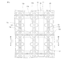
- FIG. 2 is a schematic plan view for explaining a manufacturing process of the acoustic wave device according to the first embodiment.
- FIG. 3 is a schematic plan view for explaining a manufacturing process of the acoustic wave device according to the first embodiment.
- 4 is a schematic cross-sectional view taken along line IV-IV in FIG.
- FIG. 5 is a schematic cross-sectional view taken along line VV in FIG.
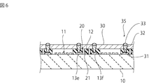
- FIG. 6 is a schematic cross-sectional view of the laminate produced in the first embodiment.
- FIG. 7 is a schematic plan view of the laminate produced in the first embodiment.
- FIG. 8 is a schematic plan view of the acoustic wave device manufactured in the first embodiment.
- FIG. 9 is a schematic cross-sectional view taken along line IX-IX in FIG.
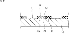
- FIG. 10 is a schematic plan view for explaining a manufacturing process of the acoustic wave device according to the second embodiment.
- FIG. 11 is a schematic cross-sectional view taken along line XI-XI in FIG.
- FIG. 12 is a schematic plan view of the acoustic wave device manufactured in the second embodiment.
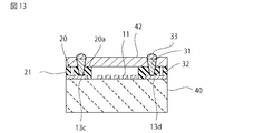
- 13 is a schematic cross-sectional view taken along line XIII-XIII in FIG.
- FIG. 14 is a schematic plan view in which the vicinity of the electrode land in FIG. 12 is enlarged.
- the acoustic wave device 1 is a surface acoustic wave device, but may be another type of acoustic wave device such as a boundary acoustic wave device.
- the mother substrate 10 is made of, for example, a piezoelectric body.
- the mother substrate 10 has piezoelectricity.
- the mother substrate 10 may be composed of a piezoelectric substrate.
- the mother substrate 10 may include a piezoelectric substrate and a non-piezoelectric layer disposed on one main surface of the piezoelectric substrate.
- the piezoelectric substrate can be made of, for example, LiTaO 3 , LiNbO 3 , quartz, or the like.
- the non-piezoelectric layer can be made of, for example, silicon oxide.
- the thickness (H 1 ) of the mother substrate 10 can be about 100 to 300 ⁇ m, for example.
- the functional element portion 11 and the connection line 12 can be formed by, for example, a sputtering method, a CVD (Chemical Vapor Deposition) method, or the like.
- the plurality of functional element portions 11 are formed in a matrix on the mother substrate 10 as shown in FIG.
- the row interval L 1 between the plurality of functional element portions 11 is preferably about 500 ⁇ m to 1800 ⁇ m.
- Row spacing L 2 of a plurality of functional elements 11 is preferably about 500 [mu] m ⁇ 1800 .mu.m.
- Each of the plurality of functional element units 11 has at least one IDT electrode and excites an elastic wave.
- the functional element unit 11 may constitute at least one of a ladder type filter unit and a longitudinally coupled resonator type elastic wave filter unit.
- the functional element unit 11 has a plurality of electrode lands 13a to 13f to which at least one IDT electrode is electrically connected.
- the plurality of electrode lands 13a to 13f are electrically connected to the connection line 12, respectively.
- connection line 12 includes a line body 12a and a connection portion 12b.
- Row spacing L 3 line body 12a is preferably about 500 [mu] m ⁇ 1800 .mu.m.
- Line spacing L 4 of the line main body 12a is preferably about 500 [mu] m ⁇ 1800 .mu.m.
- the thickness H 2 of the line main body 12a is preferably about 0.5 ⁇ m to 5 ⁇ m.
- the connection part 12b electrically connects the line body 12a and the functional element part 11 (specifically, the electrode lands 13a to 13f of the functional element part 11). Specifically, each of the electrode lands 13a to 13f is electrically connected to the line main body 12a via the connection portion 12b.
- the line width W L1 and the line width W L2 of the line body 12a and the line width W L3 of the connecting portion 12b are preferably about 5 ⁇ m to 30 ⁇ m.
- a resin support layer 20 is formed on the mother substrate 10 so as to surround each of the plurality of functional element portions 11.
- the thickness H 3 of the support layer 20 is preferably about 5 ⁇ m to 20 ⁇ m.
- the support layer 20 can be formed, for example, by patterning a resin layer formed on the entire mother substrate 10 by a screen printing method or the like using a photolithography method or the like.
- the support layer 20 can be composed of, for example, a polyimide resin, an epoxy resin, a silicone resin, or the like.
- the holding member 21 is formed so as to intersect the line main body 12a.
- the holding member 21 is formed on the mother substrate 10 so as to straddle the line main body 12a in the width direction of the line main body 12a.
- the thickness H 4 of the holding member 21 is preferably about 5 ⁇ m to 20 ⁇ m. Note that the thickness H 4 of the holding member 21 is smaller than the thickness H 3 of the support layer 20 and may not be connected to the cover.
- the widths W L4 and W L5 of the holding member 21 are preferably about 10 ⁇ m to 80 ⁇ m. Spacing D 2 of the holding member 21 is preferably about 300 [mu] m ⁇ 1700.
- the holding member 21 is not connected to the support layer 20 and has an intersecting portion 21a that intersects the line main body 12a.
- a plurality of intersecting portions 21a are provided at intervals from each other along the direction in which the line main body 12a extends.
- the extending direction of the intersecting portion 21a and the extending direction of the line main body portion 12a may be inclined, but typically, the extending direction of the intersecting portion 21a and the extending direction of the line main body 12a are orthogonal to each other. Only the crossing part 21a of the holding member 21 is provided on the line main body 12a, and the part excluding the crossing part 21 of the holding member 21 is not provided on the line main body 12a.
- the line main body 12a is exposed from the holding member 21 except for the portion covered with the intersecting portion 21a.
- the support layer 20 is not provided on the line main body 12a and covers the electrode lands 13a to 13f.
- the holding member 21 is formed by patterning using the same material as the support layer 20 and using the photolithography method simultaneously with the support layer 20 has been described. That is, the example in which the holding member 21 and the support layer 20 are integrally formed has been described. However, you may form the holding member 21 and the support layer 20 by a different material and a formation method.
- the functional element portion 11 is made to adhere to the mother substrate 10.
- the inside of the space constituted by the support layer 20 and the cover 30 is sealed.
- the thickness H 5 of the cover 30 is preferably about 10 ⁇ m to 60 ⁇ m.
- the cover 30 can be made of a material such as resin, glass, or ceramic. Note that the plate-like surface shape includes not only a flat surface but also a curved surface.
- the cover 30 is not limited to the structure formed of a single material, and may be a laminate of a plurality of layers made of different materials.
- connection line 12 may be referred to as a power supply line.
- the width W D of the dicing line L is preferably about 10 [mu] m ⁇ 50 [mu] m.
- the acoustic wave device 1 includes a piezoelectric substrate 40 (see FIG. 9) formed from a mother substrate 10. On the piezoelectric substrate 40, the functional element unit 11 is provided.
- the functional element unit 11 includes at least one IDT electrode and a plurality of electrode lands 13a to 13f to which at least one IDT electrode is electrically connected.
- the electrode lands 13a to 13f are electrically connected to an electrode portion 41 (see FIG. 8) constituted by the connection portion 12b of the connection line 12, respectively.
- the electrode portion 41 reaches the end side of the piezoelectric substrate 40.
- the support layer 20 surrounding the functional element unit 11 is provided on the piezoelectric substrate 40.
- a cover 42 supported by the support layer 20 is provided on the piezoelectric substrate 40.
- the cover 42 is formed from the cover 30.
- the dicing line L is set so that the line main body 12a is positioned on the dicing line L.
- Width W D of the mother substrate 10 is cut by the dicing saw is greater than the width W L1, W L2 of the line main body 12a. Therefore, the line main body 12a is removed by dicing, and the electrode lands 13a to 13f are electrically insulated from each other.
- the dicing saw is likely to be clogged. From this viewpoint, it is preferable not to arrange a support layer made of resin on the dicing line.
- the holding member 21 is formed so as to intersect with the line main body 12 a of the connection line 12 and not to be connected to the support layer (typically orthogonal). Further, on the dicing line L, it is desirable to make the area where the holding member 21 is not arranged larger than the area where the holding member 21 is arranged. This will be specifically described in the embodiment.
- W and area value A 1 of the cross section in the dicing region multiplied by the number of intersections to the area can be calculated by D ⁇ W L4.
- the area value A 2 of the dicing region can be calculated by W D ⁇ L 4.
- the area value A1 of the intersection is less than half of the area value A2 of the dicing region so that the area of the intersection removed by dicing is larger than the area of the region exposed to the piezoelectric substrate surface by dicing.
- leakage failure due to deformation of the holding member 21 can be suppressed by forming the holding member 21 that is not connected to the support layer 20 and performing dicing. Furthermore, peeling of the connection line 12 during dicing can be suppressed, and clogging of the dicing saw can be suppressed. As a result, it is possible to suppress the occurrence of an acoustic wave device having a leak failure and a short-circuit failure. Therefore, an elastic wave device can be manufactured with a high yield rate.
- the holding member 21 narrower than the width of the support layer 20 can be formed, clogging of the dicing saw can be suppressed, so that the interval for performing the dressing process for recovering clogging of the dicing saw is increased, or replacement of the dicing saw is performed.
- the effect of increasing the period can be obtained simultaneously with the effect of suppressing the occurrence of short circuit failure.
- the occurrence rate of short-circuit failure is compared between the example of the first embodiment and the comparative example 1 in which the holding member 21 is not provided in the first embodiment using 12,000 samples.
- the occurrence number of short-circuit defects was 0 and 0 ppm, and in Comparative Example 1, the occurrence number of short-circuit defects was 8 and was 667 ppm. Further, when the occurrence rate of leak defects is compared, in Comparative Example 1, several leak defects occur in 10,000 samples, that is, 100 ppm to 900 ppm. In the first embodiment, the leak defects occur for 10,000 samples. There were no leak failures.
- the support layer 20 is not located on the dicing line L except for the intersection 21a. For this reason, compared with the case where a resin layer is provided over the whole dicing line L etc., for example, the clogging of the dicing saw used for the dicing of the laminated body 35 hardly occurs.
- the holding member 21 is formed so as to intersect the line main body 12 a of the connection line 12, in the acoustic wave device 1, the support layer 20 is separated from the end side of the piezoelectric substrate 40.
- a plurality of intersecting portions 21 are provided at intervals in each side of each region constituting the acoustic wave device 1 of the stacked body 35. .
- the support layer 20 it is preferable to provide the support layer 20 so that the crossing portion 21 covers the end of the connection portion 12b on the line main body 12a side.
- the holding member 21 is not connected to the support layer 20, covers a part of the electrode part 41, and a part of the electrode part 41 is exposed from the holding member 21. May be.
Landscapes
- Engineering & Computer Science (AREA)
- Manufacturing & Machinery (AREA)
- Physics & Mathematics (AREA)
- Acoustics & Sound (AREA)
- Surface Acoustic Wave Elements And Circuit Networks Thereof (AREA)
Abstract
短絡不良とリーク不良の発生を少なくでき得る弾性波装置の製造方法を提供する。 圧電性を有するマザー基板10の一方主面上に、複数の機能素子部11と、複数の機能素子部11を電気的に接続する接続ライン12とを形成する。マザー基板10の一方主面上に、機能素子部11を包囲する樹脂製の支持層20を形成する。マザー基板10、機能素子部11及び支持層20を有する積層体35を、ダイシングラインに従って複数に分断することにより、機能素子部11を有する弾性波装置1を得る。接続ライン12は、ダイシングライン上に位置するライン本体12aと、ライン本体12aと機能素子部11とを電気的に接続している接続部12bとを有する。積層体35の分断に先立って、マザー基板10上に、ライン本体12aの幅方向においてライン本体12aを跨ぐ樹脂製の保持部材21を支持層20と離間して形成する。
Description
本発明は、弾性波装置の製造方法及び弾性波装置に関する。
従来、弾性波装置の製造方法として、圧電体からなるマザー基板の上に、複数の素子部を形成した後に、各素子部に分断することにより、複数の弾性波装置を同じ製造工程で製造する方法が知られている。例えば、特許文献1には、その一例が記載されている。
特許文献1に記載の製造方法では、まず、圧電体からなるマザー基板の上に、複数の素子部を形成する。素子部の形成に際しては、各素子部に電気的に接続された給電ラインを、素子部と共に形成する。次に、マザー基板の上に、各素子部を包囲するように突起部を有する支持層を形成する。次に、支持層の上に、カバー部材を配する。その後、得られた積層体を、ダイシングにより各素子部に分断することにより、複数の弾性波装置を同じ製造工程で製造する。
特許文献1に記載のように、支持層に突出部を設けることで、硬化収縮による枠状の支持層の歪みを抑制することにより、封止空間のリーク不良を抑制することができる。
しかしながら、特許文献1に記載の弾性波装置の製造方法では、ダイシングによる切削力によって、給電ラインがマザー基板から剥離し、給電ラインが除去できない問題が発生することがある。機能素子に電気的に接続される給電ラインの剥離により、短絡不良を有する弾性波装置が製造されやすくなるという問題がある。また、特許文献1に記載の弾性波装置の製造方法で突起部の数量を増やして給電ラインの剥離を防止しようとすると、ダイシングによる切削力で変形した突起部が支持体本体を変形させるため、リーク不良が発生しやすくなる問題がある。
本発明の主な目的は、短絡不良とリーク不良の発生を少なくでき得る弾性波装置の製造方法を提供することにある。
本発明に係る弾性波装置の製造方法では、圧電性を有するマザー基板の一方主面上に、複数の機能素子部と、複数の機能素子部を電気的に接続する接続ラインとを形成する。マザー基板の一方主面上に、機能素子部を包囲する樹脂製の支持層を形成する。マザー基板、機能素子部及び支持層を有する積層体を、ダイシングラインに従って複数に分断することにより、機能素子部を有する弾性波装置を得る。接続ラインは、ダイシングライン上に位置するライン本体と、ライン本体と機能素子部とを電気的に接続している接続部とを有する。積層体の分断に先立って、マザー基板上に、ライン本体の幅方向においてライン本体を跨ぐ樹脂製の保持部材を支持層と離間して形成する。
本発明に係る弾性波装置の製造方法のある特定の局面では、接続部のライン本体側端部を覆う保持部材を設ける。
本発明に係る弾性波装置の製造方法の別の特定の局面では、ダイシングラインが位置する領域において、保持部材が設けられていない面積が、保持部材が設けられた面積よりも大きくなるように保持部材を設ける。
本発明に係る弾性波装置の製造方法のさらに他の特定の局面では、保持部材と支持層とを同じ工法で形成する。
本発明に係る弾性波装置は、圧電基板と、機能素子部と、電極部と、支持層と、カバーとを備える。機能素子部は、圧電基板の一方主面上に設けられている。電極部は、機能素子部に電気的に接続されている。電極部は、圧電基板の端辺に至る。支持層は、圧電基板の一方主面上に、機能素子部を包囲するように設けられている。カバーは、支持層により支持されている。カバーは、機能素子部を覆っている。支持層は、圧電基板の端辺から離間して設けられており、機能素子部を包囲している。本発明に係る弾性波装置は、樹脂製の保持部材をさらに備える。保持部材は、圧電基板上に、支持層と離間して設けられている。保持部材は、圧電基板の端辺にまで至っている。
本発明によれば、短絡不良とリーク不良の発生を少なくでき得る弾性波装置の製造方法を提供することができる。
以下、本発明を実施した好ましい形態の一例について説明する。但し、下記の実施形態は、単なる例示である。本発明は、下記の実施形態に何ら限定されない。
また、実施形態等において参照する各図面において、実質的に同一の機能を有する部材は同一の符号で参照することとする。また、実施形態等において参照する図面は、模式的に記載されたものである。図面に描画された物体の寸法の比率などは、現実の物体の寸法の比率などとは異なる場合がある。図面相互間においても、物体の寸法比率等が異なる場合がある。具体的な物体の寸法比率等は、以下の説明を参酌して判断されるべきである。
(第1の実施形態)
本実施形態では、図8及び図9に示す弾性波装置1の製造方法について、図1~図7を主として参照しながら説明する。なお、本実施形態において、弾性波装置1は、弾性表面波装置であるが、弾性境界波装置などの他の種類の弾性波装置であってもよい。
本実施形態では、図8及び図9に示す弾性波装置1の製造方法について、図1~図7を主として参照しながら説明する。なお、本実施形態において、弾性波装置1は、弾性表面波装置であるが、弾性境界波装置などの他の種類の弾性波装置であってもよい。
まず、図1に示されるように、マザー基板10の上に、複数の機能素子部11と、接続ライン12とを形成する。マザー基板10は、例えば、圧電体からなる。マザー基板10は、圧電性を有する。マザー基板10は、圧電基板により構成されていてもよい。また、マザー基板10は、圧電基板と、圧電基板の一主面上に配された非圧電層とを有していてもよい。圧電基板は、例えば、LiTaO3やLiNbO3、水晶などにより構成することができる。非圧電層は、例えば、酸化ケイ素などにより構成することができる。マザー基板10の厚み(H1)は、例えば、100~300μm程度とすることができる。
機能素子部11と、接続ライン12とは、例えば、スパッタリング法やCVD(Chemical Vapor Deposition)法等により形成することができる。
複数の機能素子部11は、マザー基板10上において、図1に示すようにマトリクス状に形成される。複数の機能素子部11の行間隔L1は、500μm~1800μm程度であることが好ましい。複数の機能素子部11の列間隔L2は、500μm~1800μm程度であることが好ましい。
複数の機能素子部11は、それぞれ、少なくとも一つのIDT電極を有し、弾性波を励振させる。例えば、弾性波装置1が、弾性波フィルタ装置である場合は、機能素子部11は、ラダー型フィルタ部及び縦結合共振子型弾性波フィルタ部の少なくとも一方を構成していてもよい。
機能素子部11は、少なくとも一つのIDT電極が電気的に接続された複数の電極ランド13a~13fを有する。複数の電極ランド13a~13fは、それぞれ、接続ライン12に電気的に接続されている。
図1、図4に示すように、接続ライン12は、ライン本体12aと、接続部12bとを有する。ライン本体12aの列間隔L3は、500μm~1800μm程度であることが好ましい。ライン本体12aの行間隔L4は、500μm~1800μm程度であることが好ましい。ライン本体12aの厚みH2は、0.5μm~5μm程度であることが好ましい。接続部12bは、ライン本体12aと機能素子部11(詳細には、機能素子部11の電極ランド13a~13f)とを電気的に接続している。具体的には、各電極ランド13a~13fは、それぞれ、接続部12bを介してライン本体12aに電気的に接続されている。なお、ライン本体12aの線幅WL1,線幅WL2,接続部12bの線幅WL3は、5μm~30μm程度であることが好ましい。
次に、図2に示されるように、マザー基板10の上に、複数の機能素子部11のそれぞれを包囲するように樹脂製の支持層20を形成する。支持層20の厚みH3は、5μm~20μm程度であることが好ましい。支持層20は、例えば、スクリーン印刷法等によりマザー基板10の全体の上に形成した樹脂層を、フォトリソグラフィー法等を用いてパターニングすることにより形成することができる。支持層20は、例えば、ポリイミド樹脂、エポキシ樹脂、シリコーン樹脂等により構成することができる。
保持部材21は、ライン本体12aと交差するように形成される。保持部材21は、マザー基板10上に、ライン本体12aの幅方向においてライン本体12aを跨ぐように形成される。保持部材21の厚みH4は、5μm~20μm程度であることが好ましい。なお、保持部材21の厚みH4は支持層20の厚みH3より小さく、カバーに接続されていなくてもよい。保持部材21の幅WL4、WL5は、10μm~80μm程度であることが好ましい。保持部材21の間隔D2は、300μm~1700μm程度であることが好ましい。よって、保持部材21は、支持層20と接続されず、ライン本体12aと交差する交差部21aを有する。交差部21aは、ライン本体12aの延びる方向に沿って、相互に間隔をおいて複数設けられている。交差部21aの延びる方向とライン本体分12aの延びる方向とは傾斜していてもよいが、典型的には、交差部21aの延びる方向とライン本体12aの延びる方向とは直交している。ライン本体12aの上には、保持部材21のうちの交差部21aのみが設けられており、保持部材21の交差部21を除いた部分は、ライン本体12aの上に設けられていない。すなわち、ライン本体12aは、交差部21aに覆われた部分を除いて、保持部材21から露出している。また、支持層20は、ライン本体12a上に設けられず、電極ランド13a~13fを覆っている。第1の実施形態では、保持部材21を、支持層20と同じ材料を使用して、支持層20と同時にフォトリソグラフィー法を用いてパターニングして形成する例について説明した。すなわち、保持部材21と支持層20とを一体に形成する例について説明した。もっとも、保持部材21と支持層20とは、異なる材料、形成方法によって形成してもよい。
次に、図3~図5に示されるように、支持層20の上に、複数の機能素子部11を覆うように板状のカバー30を設けることにより、機能素子部11を、マザー基板10、支持層20及びカバー30によって構成される空間内部に封止する。カバー30の厚みH5は、10μm~60μm程度であることが好ましい。カバー30は、例えば、樹脂、ガラス、セラミック等の材料により構成することができる。なお、板状の表面形状は、平面だけでなく、曲面が含まれる。カバー30は単一の材料で形成される構成に限定されず、異なる材料からなる複数の層の積層体であってもよい。
次に、図6に示されるように、支持層20及びカバー30に電極ランド13a~13fに臨むビアホール31を形成する。その後、電極ランド13a~13fの露出部の上に複数のアンダーバンプメタル32とバンプ電極33とを順次形成し、図6及び図7に示す積層体35を完成させる。なお、複数のアンダーバンプメタル32は、例えば、接続ライン12を介して電極ランド13a~13fに通電し、メッキにより同時に形成することができる。従って、本発明では、接続ライン12は、給電ラインと呼ぶこともある。
次に、図7に示される列間隔L3と行間隔L4とがライン本体12aと同じ格子状であるダイシングラインLに沿って、積層体35をダイシングすることにより複数に分断する。これにより、図8及び図9に示される弾性波装置1を完成させることができる。なお、ダイシングラインLの幅WDは、10μm~50μm程度であることが好ましい。
弾性波装置1は、マザー基板10から形成された圧電基板40(図9を参照)を備える。圧電基板40の上には、機能素子部11が設けられている。機能素子部11は、少なくとも一つのIDT電極と、少なくとも一つのIDT電極が電気的に接続された複数の電極ランド13a~13fとを有する。電極ランド13a~13fには、それぞれ、接続ライン12の接続部12bから構成された電極部41(図8を参照)が電気的に接続されている。電極部41は、圧電基板40の端辺に至っている。圧電基板40の上には、機能素子部11を包囲する支持層20が設けられている。圧電基板40の上には、支持層20によって支持されたカバー42が設けられている。このカバー42は、カバー30から形成されたものである。
本実施形態では、ライン本体12aがダイシングラインL上に位置するようにダイシングラインLを設定する。マザー基板10がダイシングソーにより切削される幅WDは、ライン本体12aの幅WL1,WL2よりも大きい。このため、ダイシングにより、ライン本体12aは、除去され、電極ランド13a~13fが、互いに電気的に絶縁される。
ところで、ダイシングライン上に樹脂からなる部材があると、ダイシングソーの目詰まりが生じやすくなる。この観点からは、ダイシングライン上には、樹脂からなる支持層を配さないことが好ましい。
しかしながら、本発明者が鋭意研究した結果、ダイシングライン上に支持層に接続する突出部が設けられている場合は、製造される弾性波装置の支持層の変形により、リーク不良が生じやすいことが見出された。また、短絡不良が生じやすい原因が、接続ラインがダイシング時に剥離することにあることが見出された。
そこで、本実施形態では、図2に示されるように、接続ライン12のライン本体12aと交差し、支持層と接続しないように(典型的には直交するように)保持部材21を形成する。さらに、ダイシングラインL上において、保持部材21が配置される面積より保持部材21が配置されない面積を大きくすることが望ましい。実施形態で具体的に説明する。WD・WL4で算出できる面積に交差部の数量を乗じたダイシング領域内における交差部の面積値A1とする。WD・L4で算出できるダイシング領域の面積値A2とする。このとき、ダイシングによって除去される交差部の面積がダイシングによって圧電基板面に露出する領域の面積より大きくなるには交差部の面積値A1がダイシング領域の面積値A2の半分以下であれば好ましいため、比A2/A1の値は、2以上であることが好ましい。具体的には、D2:500μm、WD:10μm、WL4:80μm、L4:1000μm、交差部の数量:2とした実施例ではA2/A1=3.12と算出される。同様に、WD・WL3で算出できる面積に交差部の数量を乗じたダイシング領域内における交差部の面積値A3とする。WD・L3で算出できるダイシング領域の面積値A4とする。4:300、WD:10μm、WL5:50μm、L5:500μm、交差部の数量:2である実施例ではA4/A3=6.25と算出される。A1/A2及びA4/A3は3より大きいことが好ましい。また、ライン本体12aの剥離の発生を抑制するため、保持部材21を所定の間隔でライン本体12aの延びる方向に複数配置して、ライン本体12aを複数の箇所で保持することが好ましいが、保持部材21の配置箇所を増加させるとダイシングソーの目詰まりが増加する。そこで、文献1に開示された弾性波装置の製造方法において、保持部材21の幅WL4、WL5を支持層20の幅より狭い幅で形成すると、保持部材21がダイシングの切削力によって変形しやすくなる。そのため、支持層20に接続された保持部材21によって支持層20が変形し、リーク不良を有する弾性波装置が製造されてしまう。
しかしながら、支持層20と接続されていない保持部材21を形成してダイシングを実施することにより、保持部材21の変形によるリーク不良を抑制できる。さらに、ダイシング時における接続ライン12の剥離が抑制され、かつダイシンソーの目詰まりが抑制できる。その結果、リーク不良及び短絡不良を有する弾性波装置の発生を抑制できる。従って、高い良品率で弾性波装置を製造することができる。さらに、支持層20の幅より狭い保持部材21が形成できるため、ダイシンソーの目詰まりが抑制できるので、ダイシングソーの目詰まりを回復するドレッシング工程を実施する間隔が長くなる、または、ダイシングソーの交換期間が長くなる効果が、短絡不良の発生を抑制できる効果と同時に得ることができる。具体的には、第1の実施形態の実施例と、第1の実施形態において保持部材21を設けない比較例1とで、短絡不良の発生率を1万2千個の試料を使って比較すると、第1の実施形態の実施例おいて短絡不良の発生数0個で0ppmであり、比較例1において短絡不良の発生数8個で667ppmであった。また、リーク不良の発生率を比較すると、比較例1においてリーク不良が1万個の試料に数個程度、すなわち100ppm~900ppmで発生するが、第1の実施形態において1万個の試料に対してリーク不良が0個であった。さらに、第1の実施形態と、第1の実施形態においてダイシングラインの全部を支持層20で覆った比較例2とで、ダイシングソーのドレス工程の実施間隔を比較すると、第1の実施形態ではダイシングライン5本毎にダイシングソーのドレス工程の実施が必要であり、比較例2ではダイシングライン1本毎にドレス工程の実施が必要であった。目詰まりしたダイシングソーでマザー基板を切断すると、マザー基板の欠け、割れなどの問題が発生する。
また、交差部21aを除いて、支持層20は、ダイシングラインL上に位置していない。このため、例えば、樹脂層をダイシングラインL上全体にわたって設ける場合などと比較して、積層体35のダイシングに用いるダイシングソーの目詰まりも生じ難い。
このように、本実施形態では、接続ライン12のライン本体12aと交差するように保持部材21を形成するため、弾性波装置1においては、支持層20は、圧電基板40の端辺から離間して設けられており、機能素子部11を包囲する支持層本体20と、支持層20に接続されておらず、圧電基板40の端辺にまで至る保持部材21とを有する。
接続ライン12の剥離をより効果的に抑制する観点からは、積層体35の弾性波装置1を構成する各領域の各辺において、交差部21が間隔をおいて複数設けられていることが好ましい。
また、図10及び図11に示されるように、交差部21が接続部12bのライン本体12a側の端部を覆うように支持層20を設けることが好ましい。なお、図14に示されるように、保持部材21は、支持層20と接続されておらず、電極部41の一部を覆っており、電極部41の一部が保持部材21から露出していてもよい。
1…弾性波装置
10…マザー基板
11…機能素子部
12…接続ライン
12a…ライン本体
12b…接続部
13a~13f…電極ランド
20…支持層
21…保持部材
21a…交差部
30…カバー
31…ビアホール
32…アンダーバンプメタル
33…バンプ電極
35…積層体
40…圧電基板
41…電極部
42…カバー
10…マザー基板
11…機能素子部
12…接続ライン
12a…ライン本体
12b…接続部
13a~13f…電極ランド
20…支持層
21…保持部材
21a…交差部
30…カバー
31…ビアホール
32…アンダーバンプメタル
33…バンプ電極
35…積層体
40…圧電基板
41…電極部
42…カバー
Claims (5)
- 圧電性を有するマザー基板の一方主面上に、複数の機能素子部と、前記複数の機能素子部を電気的に接続する接続ラインとを形成する工程と、
前記マザー基板の一方主面上に、前記機能素子部を包囲する樹脂製の支持層を形成する工程と、
前記マザー基板、前記機能素子部及び前記支持層を有する積層体を、ダイシングラインに従って複数に分断することにより、前記機能素子部を有する弾性波装置を得る工程と、を備え、
前記接続ラインは、前記ダイシングライン上に位置するライン本体と、前記ライン本体と前記機能素子部とを電気的に接続している接続部とを有し、
前記積層体の分断に先立って、前記マザー基板上に、前記ライン本体の幅方向において前記ライン本体を跨ぐ樹脂製の保持部材を前記支持層と離間して形成する工程をさらに備える、弾性波装置の製造方法。 - 前記接続部の前記ライン本体側端部を覆う前記保持部材を設ける、請求項1に記載の弾性波装置の製造方法。
- 前記ダイシングラインが位置する領域において、前記保持部材が設けられていない面積が、前記保持部材が設けられた面積よりも大きくなるように前記保持部材を設ける、請求項1または2に記載の弾性波装置の製造方法。
- 前記保持部材と前記支持層とを同じ工法で形成する、請求項1~3のいずれか一項に記載の弾性波装置の製造方法。
- 圧電基板と、
前記圧電基板の一方主面上に設けられた機能素子部と、
前記機能素子部に電気的に接続されており、前記圧電基板の端辺に至る電極部と、
前記圧電基板の一方主面上に、前記機能素子部を包囲するように設けられた支持層と、
前記支持層により支持されており、前記機能素子部を覆うカバーと、
を備え、
前記支持層は、前記圧電基板の端辺から離間して設けられており、前記機能素子部を包囲しており、
前記圧電基板上に、前記支持層と離間して設けられており、前記圧電基板の端辺にまで至る樹脂製の保持部材をさらに備える、弾性波装置。
Priority Applications (4)
| Application Number | Priority Date | Filing Date | Title |
|---|---|---|---|
| JP2014550985A JP6044643B2 (ja) | 2012-12-05 | 2013-10-22 | 弾性波装置の製造方法及び弾性波装置 |
| CN201380060102.6A CN104798302B (zh) | 2012-12-05 | 2013-10-22 | 弹性波装置的制造方法以及弹性波装置 |
| US14/705,029 US10320355B2 (en) | 2012-12-05 | 2015-05-06 | Method of manufacturing elastic wave device |
| US16/400,111 US10644669B2 (en) | 2012-12-05 | 2019-05-01 | Elastic wave device |
Applications Claiming Priority (2)
| Application Number | Priority Date | Filing Date | Title |
|---|---|---|---|
| JP2012-266376 | 2012-12-05 | ||
| JP2012266376 | 2012-12-05 |
Related Child Applications (1)
| Application Number | Title | Priority Date | Filing Date |
|---|---|---|---|
| US14/705,029 Continuation US10320355B2 (en) | 2012-12-05 | 2015-05-06 | Method of manufacturing elastic wave device |
Publications (1)
| Publication Number | Publication Date |
|---|---|
| WO2014087752A1 true WO2014087752A1 (ja) | 2014-06-12 |
Family
ID=50883180
Family Applications (1)
| Application Number | Title | Priority Date | Filing Date |
|---|---|---|---|
| PCT/JP2013/078521 Ceased WO2014087752A1 (ja) | 2012-12-05 | 2013-10-22 | 弾性波装置の製造方法及び弾性波装置 |
Country Status (4)
| Country | Link |
|---|---|
| US (2) | US10320355B2 (ja) |
| JP (1) | JP6044643B2 (ja) |
| CN (1) | CN104798302B (ja) |
| WO (1) | WO2014087752A1 (ja) |
Cited By (2)
| Publication number | Priority date | Publication date | Assignee | Title |
|---|---|---|---|---|
| JPWO2017098809A1 (ja) * | 2015-12-11 | 2018-08-30 | 株式会社村田製作所 | 弾性波装置 |
| JP2022182128A (ja) * | 2021-05-27 | 2022-12-08 | 日清紡マイクロデバイス株式会社 | 電子デバイスの製造方法 |
Citations (4)
| Publication number | Priority date | Publication date | Assignee | Title |
|---|---|---|---|---|
| JP2002261582A (ja) * | 2000-10-04 | 2002-09-13 | Matsushita Electric Ind Co Ltd | 弾性表面波デバイスおよびその製造方法ならびにそれを用いた回路モジュール |
| JP2006333130A (ja) * | 2005-05-26 | 2006-12-07 | Alps Electric Co Ltd | 表面弾性波装置 |
| JP2008135999A (ja) * | 2006-11-28 | 2008-06-12 | Fujitsu Media Device Kk | 弾性波デバイスおよびその製造方法 |
| WO2012132147A1 (ja) * | 2011-03-28 | 2012-10-04 | 株式会社村田製作所 | 電子部品及びその製造方法 |
Family Cites Families (17)
| Publication number | Priority date | Publication date | Assignee | Title |
|---|---|---|---|---|
| JPH0756927B2 (ja) * | 1988-12-16 | 1995-06-14 | 株式会社村田製作所 | 弾性表面波素子の製造方法 |
| JP2001094390A (ja) * | 1999-09-20 | 2001-04-06 | Toshiba Corp | 弾性表面波デバイスおよびその製造方法 |
| US6710682B2 (en) * | 2000-10-04 | 2004-03-23 | Matsushita Electric Industrial Co., Ltd. | Surface acoustic wave device, method for producing the same, and circuit module using the same |
| JP3797144B2 (ja) * | 2001-06-25 | 2006-07-12 | 株式会社村田製作所 | 弾性表面波装置 |
| US7156741B2 (en) * | 2003-01-31 | 2007-01-02 | Wms Gaming, Inc. | Gaming device for wagering on multiple game outcomes |
| JP4210958B2 (ja) * | 2004-07-14 | 2009-01-21 | 株式会社村田製作所 | 圧電デバイス |
| EP1892831B1 (en) * | 2005-06-16 | 2012-08-29 | Murata Manufacturing Co., Ltd. | Piezoelectric device and manufacturing method thereof |
| JP4712632B2 (ja) * | 2006-07-24 | 2011-06-29 | 太陽誘電株式会社 | 弾性波デバイス及びその製造方法 |
| WO2009078137A1 (ja) * | 2007-12-14 | 2009-06-25 | Murata Manufacturing Co., Ltd. | 表面波装置及びその製造方法 |
| JP4484934B2 (ja) | 2008-02-26 | 2010-06-16 | 富士通メディアデバイス株式会社 | 電子部品及びその製造方法 |
| JP4664397B2 (ja) * | 2008-06-24 | 2011-04-06 | 日本電波工業株式会社 | 圧電部品及びその製造方法 |
| WO2010047031A1 (ja) * | 2008-10-24 | 2010-04-29 | 株式会社 村田製作所 | 電子部品、およびその製造方法 |
| US8334737B2 (en) * | 2009-07-15 | 2012-12-18 | Panasonic Corporation | Acoustic wave device and electronic apparatus using the same |
| WO2011065499A1 (ja) * | 2009-11-27 | 2011-06-03 | 京セラ株式会社 | 弾性波装置およびその製造方法 |
| JP2012009991A (ja) * | 2010-06-23 | 2012-01-12 | Murata Mfg Co Ltd | 弾性波素子の製造方法 |
| DE102012112058B4 (de) * | 2012-12-11 | 2020-02-27 | Snaptrack, Inc. | MEMS-Bauelement und Verfahren zur Verkapselung von MEMS-Bauelementen |
| KR101825499B1 (ko) * | 2013-08-13 | 2018-02-05 | 가부시키가이샤 무라타 세이사쿠쇼 | 탄성파 장치 |
-
2013
- 2013-10-22 JP JP2014550985A patent/JP6044643B2/ja active Active
- 2013-10-22 CN CN201380060102.6A patent/CN104798302B/zh active Active
- 2013-10-22 WO PCT/JP2013/078521 patent/WO2014087752A1/ja not_active Ceased
-
2015
- 2015-05-06 US US14/705,029 patent/US10320355B2/en active Active
-
2019
- 2019-05-01 US US16/400,111 patent/US10644669B2/en active Active
Patent Citations (4)
| Publication number | Priority date | Publication date | Assignee | Title |
|---|---|---|---|---|
| JP2002261582A (ja) * | 2000-10-04 | 2002-09-13 | Matsushita Electric Ind Co Ltd | 弾性表面波デバイスおよびその製造方法ならびにそれを用いた回路モジュール |
| JP2006333130A (ja) * | 2005-05-26 | 2006-12-07 | Alps Electric Co Ltd | 表面弾性波装置 |
| JP2008135999A (ja) * | 2006-11-28 | 2008-06-12 | Fujitsu Media Device Kk | 弾性波デバイスおよびその製造方法 |
| WO2012132147A1 (ja) * | 2011-03-28 | 2012-10-04 | 株式会社村田製作所 | 電子部品及びその製造方法 |
Cited By (3)
| Publication number | Priority date | Publication date | Assignee | Title |
|---|---|---|---|---|
| JPWO2017098809A1 (ja) * | 2015-12-11 | 2018-08-30 | 株式会社村田製作所 | 弾性波装置 |
| JP2022182128A (ja) * | 2021-05-27 | 2022-12-08 | 日清紡マイクロデバイス株式会社 | 電子デバイスの製造方法 |
| JP7712796B2 (ja) | 2021-05-27 | 2025-07-24 | 日清紡マイクロデバイス株式会社 | 電子デバイスの製造方法 |
Also Published As
| Publication number | Publication date |
|---|---|
| JP6044643B2 (ja) | 2016-12-14 |
| US20190260341A1 (en) | 2019-08-22 |
| CN104798302A (zh) | 2015-07-22 |
| US10644669B2 (en) | 2020-05-05 |
| US20150236237A1 (en) | 2015-08-20 |
| CN104798302B (zh) | 2017-07-07 |
| JPWO2014087752A1 (ja) | 2017-01-05 |
| US10320355B2 (en) | 2019-06-11 |
Similar Documents
| Publication | Publication Date | Title |
|---|---|---|
| JP5880529B2 (ja) | 弾性表面波フィルタ | |
| US20160329878A1 (en) | Acoustic wave device | |
| CN101911485B (zh) | 压电器件 | |
| JP5838131B2 (ja) | タッチオンレンズデバイスを製造するための方法 | |
| JP5591163B2 (ja) | 弾性波装置およびその製造方法 | |
| US8421307B2 (en) | Acoustic wave device | |
| JP6026829B2 (ja) | 弾性表面波デバイス | |
| JP5818946B2 (ja) | 弾性波装置 | |
| JP2012029262A (ja) | 圧電振動片及びその製造方法 | |
| US10644669B2 (en) | Elastic wave device | |
| JP5848079B2 (ja) | 弾性波デバイス及びその製造方法 | |
| JPWO2014171369A1 (ja) | 弾性表面波装置 | |
| JP2021027383A (ja) | 弾性波装置 | |
| JP6166190B2 (ja) | 弾性波素子および弾性波装置 | |
| JP5596970B2 (ja) | 弾性波装置及びその製造方法 | |
| JP7712796B2 (ja) | 電子デバイスの製造方法 | |
| JP2011109481A (ja) | 弾性波デバイスおよびその製造方法 | |
| JP2015039204A (ja) | 弾性波装置およびその製造方法 | |
| JP2007028196A (ja) | 弾性境界波装置の製造方法及び弾性境界波装置 | |
| JP2010258555A (ja) | 弾性境界波装置の製造方法 | |
| JP6352844B2 (ja) | 多数個取り回路配線基板および弾性表面波装置 | |
| WO2023157798A1 (ja) | 弾性波装置 | |
| WO2018079485A1 (ja) | 弾性波装置 | |
| JP6460706B2 (ja) | 弾性表面波デバイスの製造方法 | |
| JP6068220B2 (ja) | 電子部品の製造方法 |
Legal Events
| Date | Code | Title | Description |
|---|---|---|---|
| 121 | Ep: the epo has been informed by wipo that ep was designated in this application |
Ref document number: 13859880 Country of ref document: EP Kind code of ref document: A1 |
|
| ENP | Entry into the national phase |
Ref document number: 2014550985 Country of ref document: JP Kind code of ref document: A |
|
| NENP | Non-entry into the national phase |
Ref country code: DE |
|
| 122 | Ep: pct application non-entry in european phase |
Ref document number: 13859880 Country of ref document: EP Kind code of ref document: A1 |