WO2014065068A1 - 発光装置 - Google Patents
発光装置 Download PDFInfo
- Publication number
- WO2014065068A1 WO2014065068A1 PCT/JP2013/075872 JP2013075872W WO2014065068A1 WO 2014065068 A1 WO2014065068 A1 WO 2014065068A1 JP 2013075872 W JP2013075872 W JP 2013075872W WO 2014065068 A1 WO2014065068 A1 WO 2014065068A1
- Authority
- WO
- WIPO (PCT)
- Prior art keywords
- light emitting
- substrate
- light
- emitting device
- ceramic
- Prior art date
- Legal status (The legal status is an assumption and is not a legal conclusion. Google has not performed a legal analysis and makes no representation as to the accuracy of the status listed.)
- Ceased
Links
Images



Classifications
-
- H—ELECTRICITY
- H10—SEMICONDUCTOR DEVICES; ELECTRIC SOLID-STATE DEVICES NOT OTHERWISE PROVIDED FOR
- H10H—INORGANIC LIGHT-EMITTING SEMICONDUCTOR DEVICES HAVING POTENTIAL BARRIERS
- H10H20/00—Individual inorganic light-emitting semiconductor devices having potential barriers, e.g. light-emitting diodes [LED]
- H10H20/80—Constructional details
- H10H20/85—Packages
- H10H20/858—Means for heat extraction or cooling
- H10H20/8585—Means for heat extraction or cooling being an interconnection
-
- H—ELECTRICITY
- H10—SEMICONDUCTOR DEVICES; ELECTRIC SOLID-STATE DEVICES NOT OTHERWISE PROVIDED FOR
- H10H—INORGANIC LIGHT-EMITTING SEMICONDUCTOR DEVICES HAVING POTENTIAL BARRIERS
- H10H20/00—Individual inorganic light-emitting semiconductor devices having potential barriers, e.g. light-emitting diodes [LED]
- H10H20/80—Constructional details
- H10H20/85—Packages
- H10H20/8506—Containers
-
- H—ELECTRICITY
- H10—SEMICONDUCTOR DEVICES; ELECTRIC SOLID-STATE DEVICES NOT OTHERWISE PROVIDED FOR
- H10H—INORGANIC LIGHT-EMITTING SEMICONDUCTOR DEVICES HAVING POTENTIAL BARRIERS
- H10H20/00—Individual inorganic light-emitting semiconductor devices having potential barriers, e.g. light-emitting diodes [LED]
- H10H20/80—Constructional details
- H10H20/85—Packages
- H10H20/857—Interconnections, e.g. lead-frames, bond wires or solder balls
-
- H—ELECTRICITY
- H10—SEMICONDUCTOR DEVICES; ELECTRIC SOLID-STATE DEVICES NOT OTHERWISE PROVIDED FOR
- H10W—GENERIC PACKAGES, INTERCONNECTIONS, CONNECTORS OR OTHER CONSTRUCTIONAL DETAILS OF DEVICES COVERED BY CLASS H10
- H10W90/00—Package configurations
-
- H—ELECTRICITY
- H10—SEMICONDUCTOR DEVICES; ELECTRIC SOLID-STATE DEVICES NOT OTHERWISE PROVIDED FOR
- H10H—INORGANIC LIGHT-EMITTING SEMICONDUCTOR DEVICES HAVING POTENTIAL BARRIERS
- H10H20/00—Individual inorganic light-emitting semiconductor devices having potential barriers, e.g. light-emitting diodes [LED]
- H10H20/80—Constructional details
- H10H20/85—Packages
- H10H20/852—Encapsulations
- H10H20/853—Encapsulations characterised by their shape
-
- H—ELECTRICITY
- H10—SEMICONDUCTOR DEVICES; ELECTRIC SOLID-STATE DEVICES NOT OTHERWISE PROVIDED FOR
- H10H—INORGANIC LIGHT-EMITTING SEMICONDUCTOR DEVICES HAVING POTENTIAL BARRIERS
- H10H20/00—Individual inorganic light-emitting semiconductor devices having potential barriers, e.g. light-emitting diodes [LED]
- H10H20/80—Constructional details
- H10H20/85—Packages
- H10H20/855—Optical field-shaping means, e.g. lenses
- H10H20/856—Reflecting means
-
- H—ELECTRICITY
- H10—SEMICONDUCTOR DEVICES; ELECTRIC SOLID-STATE DEVICES NOT OTHERWISE PROVIDED FOR
- H10H—INORGANIC LIGHT-EMITTING SEMICONDUCTOR DEVICES HAVING POTENTIAL BARRIERS
- H10H20/00—Individual inorganic light-emitting semiconductor devices having potential barriers, e.g. light-emitting diodes [LED]
- H10H20/80—Constructional details
- H10H20/85—Packages
- H10H20/858—Means for heat extraction or cooling
- H10H20/8581—Means for heat extraction or cooling characterised by their material
-
- H—ELECTRICITY
- H10—SEMICONDUCTOR DEVICES; ELECTRIC SOLID-STATE DEVICES NOT OTHERWISE PROVIDED FOR
- H10W—GENERIC PACKAGES, INTERCONNECTIONS, CONNECTORS OR OTHER CONSTRUCTIONAL DETAILS OF DEVICES COVERED BY CLASS H10
- H10W72/00—Interconnections or connectors in packages
- H10W72/50—Bond wires
- H10W72/551—Materials of bond wires
- H10W72/552—Materials of bond wires comprising metals or metalloids, e.g. silver
- H10W72/5522—Materials of bond wires comprising metals or metalloids, e.g. silver comprising gold [Au]
-
- H—ELECTRICITY
- H10—SEMICONDUCTOR DEVICES; ELECTRIC SOLID-STATE DEVICES NOT OTHERWISE PROVIDED FOR
- H10W—GENERIC PACKAGES, INTERCONNECTIONS, CONNECTORS OR OTHER CONSTRUCTIONAL DETAILS OF DEVICES COVERED BY CLASS H10
- H10W90/00—Package configurations
- H10W90/701—Package configurations characterised by the relative positions of pads or connectors relative to package parts
- H10W90/751—Package configurations characterised by the relative positions of pads or connectors relative to package parts of bond wires
- H10W90/753—Package configurations characterised by the relative positions of pads or connectors relative to package parts of bond wires between laterally-adjacent chips
Definitions
- the present invention relates to a light emitting device including a light emitting element formed on a substrate.
- a light-emitting device including a light-emitting element formed on a substrate a light-emitting device using a ceramic substrate, a light-emitting device including an organic resist layer as an insulating layer on a metal substrate, and the like are known.
- Patent Document 1 in order to form a laminated plate having tracking resistance, a ceramic layer is formed by spraying ceramic on one side of a copper foil, an adhesive is applied to the ceramic layer, and an adhesive is applied.
- a technique for laminating a paper-based phenol resin-impregnated coated fabric on the surface is disclosed.
- Patent Document 2 discloses a thermoelectric conversion device using a metal substrate on which an insulating coating layer made of a ceramic paint is formed.
- Patent Document 3 discloses a technique for forming an insulating film by applying a ceramic paint to a substrate such as an aluminum plate.
- Japanese Patent Publication Japanese Patent Publication “Japanese Laid-Open Patent Publication No. 1-156056 (published on June 19, 1989)” Japanese Patent Publication “Japanese Patent Laid-Open No. 2006-66822 (published on March 9, 2006)” Japanese Patent Publication “JP 59-149958 A (published on August 28, 1984)”
- an organic resist that has been conventionally used as an insulating layer on a substrate of a light emitting device has a problem that sufficient thermal conductivity, heat resistance, and light resistance cannot be obtained.
- a configuration using a conventional organic resist as the insulating layer provides sufficient light reflectivity. I can't.
- the present invention has been made in view of the above-described problems, and an object thereof is to improve heat dissipation and light utilization efficiency in a light emitting device including a light emitting element formed on a substrate.
- a light-emitting device is a light-emitting device including a substrate and a light-emitting element disposed on the substrate, the thermal conductivity formed by applying a ceramic paint on the substrate. And a ceramic insulating film having light reflectivity, wherein the light emitting element is disposed on the ceramic insulating film.
- FIG. 1A is a top view showing a configuration example of the light emitting device 30 according to this embodiment
- FIG. 1B is a cross-sectional view taken along the line AA shown in FIG.
- the light emitting device 30 includes a substrate 100, a light emitting element (semiconductor light emitting element) 110, a light reflecting resin frame 130, a sealing resin 140, and a ceramic insulating film 150 having a single layer structure.
- the substrate 100 is a substrate made of a material having high thermal conductivity.
- the material of the substrate 100 is not particularly limited as long as it is a material having high thermal conductivity.
- a substrate made of a metal such as aluminum or copper can be used.
- an aluminum substrate is used because it is inexpensive, easy to process, and strong against atmospheric humidity.
- the outer shape of the substrate 100 is a hexagon.
- the outer shape of the substrate 100 is not limited to this, and may be other polygons such as a triangle, a quadrangle, a pentagon, and an octagon. Alternatively, it may be circular or elliptical, or may have other shapes.
- the ceramic insulating film 150 is a film formed on one surface (hereinafter referred to as a surface) of the substrate 100 by a printing method, and has electrical insulation, high light reflectivity, and high thermal conductivity.
- a light emitting element 110 On the surface of the ceramic insulating film 150, a light emitting element 110, a light reflecting resin frame 130, and a sealing resin 140 are provided. Furthermore, anode conductor wiring 160, cathode conductor wiring 165, anode electrode 170 and cathode electrode 180 as land portions, alignment mark 190, polarity mark 195, and the like are directly formed on the surface of ceramic insulating film 150. ing.
- a protective element (not shown) connected in parallel with a circuit in which a plurality of light emitting elements 110 are connected in series is provided on the surface of the ceramic insulating film 150 as a resistance element for protecting the light emitting elements 110 from electrostatic withstand voltage. Further, it may be formed.
- the protective element can be formed by, for example, a printing resistor or a Zener diode. When a Zener diode is used as the protective element, the Zener diode is die-bonded on the wiring pattern and further electrically connected to a desired wiring by wire bonding. Also in this case, the Zener diode is connected in parallel to a circuit in which a plurality of light emitting elements 110 are connected in series.
- the light emitting element 110 is a semiconductor light emitting element such as an LED (Light Emitting Diode), and in this embodiment, a blue light emitting element having an emission peak wavelength of around 450 nm is used.
- the configuration of the light emitting element 110 is not limited to this, and for example, an ultraviolet (near ultraviolet) light emitting element having an emission peak wavelength of 390 nm to 420 nm may be used. By using the above ultraviolet (near ultraviolet) light emitting element, the luminous efficiency can be further improved.
- a plurality (20 in this embodiment) of light emitting elements 110 are mounted at predetermined positions that can satisfy a predetermined light emission amount on the surface of the ceramic insulating film 150.
- Electrical connection of the light emitting element 110 (such as the anode conductor wiring 160 and the cathode conductor wiring 165) is performed by wire bonding using wires.
- a gold wire can be used as the wire.
- the light reflecting resin frame 130 forms an annular (arc-shaped) light reflecting resin frame 130 made of an alumina filler-containing silicone resin.
- the material of the light reflecting resin frame 130 is not limited to this, and any insulating resin having light reflecting characteristics may be used.
- the shape of the light reflecting resin frame 130 is not limited to an annular shape (arc shape), and may be an arbitrary shape. The same applies to the shapes of the anode conductor wiring 160, the cathode conductor wiring 165, and the protection element.
- the sealing resin 140 is a sealing resin layer made of a translucent resin, and is formed by filling a region surrounded by the light reflecting resin frame 130, and seals the ceramic insulating film 150, the light emitting element 110, the wire, and the like. Stop.
- the sealing resin 140 may contain a phosphor.
- a phosphor that is excited by the primary light emitted from the light emitting element 110 and emits light having a longer wavelength than the primary light is used.
- the configuration of the phosphor is not particularly limited, and can be appropriately selected according to the desired white chromaticity. For example, as a combination of daylight white color or light bulb color, a combination of YAG yellow phosphor and (Sr, Ca) AlSiN 3 : Eu red phosphor, a combination of YAG yellow phosphor and CaAlSiN 3 : Eu red phosphor, etc. Can be used.
- a combination of (Sr, Ca) AlSiN 3 : Eu red phosphor and Ca 3 (Sc, Mg) 2 Si 3 O 12 : Ce green phosphor can be used.
- the combination of another fluorescent substance may be used and the structure containing only a YAG yellow fluorescent substance as pseudo white may be used.
- the light emitting element 110 and the electrode portion are formed on the surface of the ceramic insulating film 150.
- a sealing resin 140 that seals a member (a part of the ceramic insulating film 150, the light emitting element 110, and a wire) is directly formed. That.
- a ceramic insulating film 150 having a thickness of 100 ⁇ m is formed on one surface of a substrate 100 made of aluminum by a printing method. Specifically, after a ceramic coating is printed on one surface of the substrate 100 (film thickness of 20 ⁇ m or more), the ceramic insulating film 150 is formed through a drying process and a firing process. As the ceramic coating, it is preferable to use a coating that exhibits electrical insulation, high thermal conductivity, and high light reflectivity after the firing step. Further, the ceramic paint includes a caking agent for attaching the ceramic paint to the substrate 100, a resin for facilitating printing, and a solvent for maintaining the viscosity.
- the anode conductor wiring 160, the cathode conductor wiring 165, the anode electrode 170 and the cathode electrode 180 as the land portion, the alignment mark 190, and the polarity mark 195 are formed on the ceramic insulating film 150 by a screen printing method. To do.
- the anode conductor wiring 160, the cathode conductor wiring 165, the alignment mark 190, and the polarity mark 195 are Ag (silver) having a thickness of 1.0 ⁇ m and Ni having a thickness of 2.0 ⁇ m. (Nickel) and 0.3 ⁇ m thick Au (gold) were formed. Further, as the anode electrode 170 and the cathode electrode 180 as the land portions, Ag (silver) having a thickness of 1.0 ⁇ m, Cu (copper) having a thickness of 20 ⁇ m, Ni (nickel) having a thickness of 2.0 ⁇ m, A 0.3 ⁇ m thick Au (gold) was formed.
- each light emitting element 110 is fixed on the ceramic insulating film 150 using a resin paste.
- each light emitting element 110 is connected by a wire, and the conductor wiring 160 and the light emitting element 110 are wire-bonded for electrical connection.
- a light reflecting resin frame 130 is formed on the substrate 100, the anode conductor wiring 160, and the cathode conductor wiring 165 so as to surround the periphery of the mounting region of the light emitting element 110.
- the formation method of the light reflection resin frame 130 is not particularly limited, and a conventionally known method can be used.
- the sealing resin 140 is filled in the region surrounded by the light reflecting resin frame 130, and the ceramic insulating film 150, the light emitting element 110, the wire, and the like in the region are sealed.
- the reflectance of the ceramic insulating film 150 formed in this embodiment is about 4% higher than the reflectance of the substrate 100 made of aluminum.
- the thickness of the ceramic insulating film 150 is determined based on the reflectance and the dielectric strength voltage. If the ceramic insulating film 150 is too thick, cracks may occur. If the ceramic insulating film 150 is too thin, sufficient reflectance and dielectric strength may not be obtained. For this reason, the thickness of the ceramic insulating film 150 formed on the substrate 100 is 20 ⁇ m or more in order to ensure the reflectance in the visible light region and the insulation between the light emitting element 110 and the substrate 100 and to prevent the occurrence of cracks. It is preferably 130 or less, and more preferably 50 ⁇ m or more and 100 ⁇ m or less.
- the ceramic insulating film 150 having a single layer structure is formed on the substrate 100.
- the multilayered ceramic insulating film 150 including a plurality of ceramic layers is formed on the substrate 100.
- FIG. 2A is a top view showing a configuration example of the light emitting device 10 according to the present embodiment
- FIG. 2B is a cross-sectional view taken along the line BB shown in FIG.
- the light emitting device 10 includes a substrate 100, a light emitting element (semiconductor light emitting element) 110, a light reflecting resin frame 130, a sealing resin 140, and a multilayer ceramic insulating film 150.
- the light emitting device 10 has a (i) multilayer structure in which the ceramic insulating film 150 includes a ceramic layer (first ceramic layer) 150b having high thermal conductivity and a ceramic layer (second ceramic layer) 150a having high light reflectivity. And (ii) the outer shape of the substrate 100 is different from the light emitting device 30 of the first embodiment, but the other points are substantially the same.
- the substrate 100 is a substrate made of a material having high thermal conductivity.
- the material of the substrate 100 is not particularly limited as long as it is a material having high thermal conductivity.
- a substrate made of a metal such as aluminum or copper can be used.
- an aluminum substrate is used as in the first embodiment.
- the ceramic insulating film 150 is a film having a multilayer structure in which a high thermal conductive ceramic layer 150b and a high light reflective ceramic layer 150a are stacked on the substrate 100.
- the ceramic insulating film 150 having high thermal conductivity and high light reflectivity is formed by laminating the above two different ceramic layers to form a multilayer structure.
- the high thermal conductivity ceramic layer 150b and the high light reflection ceramic layer 150a are preferably formed by forming the high thermal conductivity ceramic layer 150b on the substrate 100 and forming the high light reflection ceramic layer 150a thereon.
- it is preferable that at least one of the high thermal conductive ceramic layer 150b and the high light reflective ceramic layer 150a has electrical insulation.
- a light emitting element 110 On the surface of the ceramic insulating film 150, a light emitting element 110, a light reflecting resin frame 130, and a sealing resin 140 are provided. Furthermore, anode conductor wiring 160, cathode conductor wiring 165, anode electrode 170 and cathode electrode 180 as land portions, alignment mark 190, polarity mark 195, and the like are directly formed on the surface of ceramic insulating film 150. ing.
- a protective element (not shown) connected in parallel with a circuit in which a plurality of light emitting elements 110 are connected in series is provided on the surface of the ceramic insulating film 150 as a resistance element for protecting the light emitting elements 110 from electrostatic withstand voltage. Further, it may be formed.
- the protective element can be formed by, for example, a printing resistor or a Zener diode. When a Zener diode is used as the protective element, the Zener diode is die-bonded on the wiring pattern and further electrically connected to a desired wiring by wire bonding. Also in this case, the Zener diode is connected in parallel to a circuit in which a plurality of light emitting elements 110 are connected in series.
- the light emitting element 110 is a semiconductor light emitting element such as an LED (Light Emitting Diode), and in this embodiment, a blue light emitting element having an emission peak wavelength of around 450 nm is used.
- the configuration of the light emitting element 110 is not limited to this, and for example, an ultraviolet (near ultraviolet) light emitting element having an emission peak wavelength of 390 nm to 420 nm may be used. By using the above ultraviolet (near ultraviolet) light emitting element, the luminous efficiency can be further improved.
- a plurality of light emitting elements 110 are mounted on the surface of the highly light-reflective ceramic layer 150a at predetermined positions that satisfy a predetermined light emission amount. Electrical connection of the light emitting element 110 (such as the anode conductor wiring 160 and the cathode conductor wiring 165) is performed by wire bonding using wires. For example, a gold wire can be used as the wire.
- the light reflecting resin frame 130 forms an annular (arc-shaped) light reflecting resin frame 130 made of an alumina filler-containing silicone resin.
- the material of the light reflecting resin frame 130 is not limited to this, and any insulating resin having light reflecting characteristics may be used.
- the shape of the light reflecting resin frame 130 is not limited to an annular shape (arc shape), and may be an arbitrary shape. The same applies to the shapes of the anode conductor wiring 160, the cathode conductor wiring 165, and the protection element.
- the sealing resin 140 is a sealing resin layer made of a translucent resin, and is formed by filling a region surrounded by the light reflecting resin frame 130, and seals the ceramic insulating film 150, the light emitting element 110, the wire, and the like. Stop.
- the sealing resin 140 may contain a phosphor.
- a phosphor that is excited by the primary light emitted from the light emitting element 110 and emits light having a longer wavelength than the primary light is used.
- the configuration of the phosphor is not particularly limited, and can be appropriately selected according to the desired white chromaticity. For example, as a combination of daylight white color or light bulb color, a combination of YAG yellow phosphor and (Sr, Ca) AlSiN 3 : Eu red phosphor, a combination of YAG yellow phosphor and CaAlSiN 3 : Eu red phosphor, etc. Can be used.
- a combination of (Sr, Ca) AlSiN 3 : Eu red phosphor and Ca 3 (Sc, Mg) 2 Si 3 O 12 : Ce green phosphor can be used.
- the combination of another fluorescent substance may be used and the structure containing only a YAG yellow fluorescent substance as pseudo white may be used.
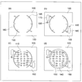
- FIG. 3 is an explanatory diagram illustrating a manufacturing process of the light emitting device 10.
- a high thermal conductive ceramic layer 150b having a thickness of 50 ⁇ m is formed on one surface of a substrate 100 made of aluminum by a printing method. Specifically, after a ceramic coating to be the high thermal conductivity ceramic layer 150b is printed on one surface of the substrate 100 (film thickness of 20 ⁇ m or more), the high thermal conductivity ceramic layer 150b is formed through a drying step and a firing step. .
- the coating material which shows high heat conductivity after a baking process is used as said ceramic coating material.
- the ceramic paint includes a caking agent for attaching the ceramic paint to the substrate 100, a resin for facilitating printing, and a solvent for maintaining the viscosity.
- a high light reflective ceramic layer 150a having a thickness of 50 ⁇ m is formed on the high thermal conductive ceramic layer 150b by a printing method. Specifically, after a ceramic coating that becomes the high light reflective ceramic layer 150a is printed on the high thermal conductive ceramic layer 150b (film thickness of 20 ⁇ m or more), it is formed through a drying step and a firing step.
- the coating material which shows high light reflectivity after a baking process is used as said ceramic paint.
- the ceramic paint includes a caking agent for attaching the ceramic paint to the substrate 100, a resin for facilitating printing, and a solvent for maintaining the viscosity.
- the anode conductor wiring 160, the cathode conductor wiring 165, and the alignment mark 190 are formed on the ceramic insulating film 150 (highly light-reflective ceramic layer 150a) by a screen printing method (FIG. 3A). reference). Thereafter, the anode electrode 170 and the cathode electrode 180 as the land portion, and the polarity mark 195 are formed by a screen printing method (see FIG. 3B).
- the anode conductor wiring 160, the cathode conductor wiring 165, the alignment mark 190, and the polarity mark 195 are Ag (silver) having a thickness of 1.0 ⁇ m and Ni having a thickness of 2.0 ⁇ m. (Nickel) and 0.3 ⁇ m thick Au (gold) were formed. Further, as the anode electrode 170 and the cathode electrode 180 as the land portions, Ag (silver) having a thickness of 1.0 ⁇ m, Cu (copper) having a thickness of 20 ⁇ m, Ni (nickel) having a thickness of 2.0 ⁇ m, A 0.3 ⁇ m thick Au (gold) was formed.
- the plurality of light emitting elements 110 are fixed on the ceramic insulating film 150 (highly reflective ceramic layer 150a) using a resin paste. Further, each light emitting element 110 is connected by a wire, and the conductor wirings 160 and 165 and the light emitting element 110 are wire-bonded for electrical connection (see FIG. 3C).
- a light reflecting resin frame 130 is formed on the substrate 100, the anode conductor wiring 160, and the cathode conductor wiring 165 so as to surround the periphery of the mounting region of the light emitting element 110.
- the formation method of the light reflection resin frame 130 is not particularly limited, and a conventionally known method can be used.
- the sealing resin 140 is filled in the region surrounded by the light reflecting resin frame 130, and the ceramic insulating film 150, the light emitting element 110, the wire, and the like in the region are sealed (see FIG. 3D).
- the reflectance (reflectance of light having a wavelength of 450 nm) of the ceramic insulating film 150 (highly light-reflective ceramic layer 150a) formed in this embodiment is about 4% as compared with the reflectance of the substrate 100 made of aluminum. high.
- the thickness of the high light reflective ceramic layer 150a and the high thermal conductivity ceramic layer 150b is too thick, cracks may occur. If the thickness is too thin, sufficient light reflection characteristics, thermal conductivity, and dielectric strength can be obtained. It may not be possible. For this reason, in the present embodiment, in consideration of characteristics required for the high light reflective ceramic layer 150a and the high thermal conductivity ceramic layer 150b (high light reflectivity, high thermal conductivity, withstand voltage), and prevention of occurrence of cracks, The thickness of each of these layers was 50 ⁇ m. In addition, when it is desired to prioritize one of the characteristics of high light reflectivity or high thermal conductivity, the thickness of any layer may be set thick.
- the thickness of each layer should be set to 10 ⁇ m or more and 65 ⁇ m or less, respectively. Is preferable, and is more preferably set to 25 ⁇ m or more and 50 ⁇ m or less. In order to prevent the occurrence of cracks more reliably, the total thickness of the high light reflective ceramic layer 150a and the high thermal conductive ceramic layer 150b is preferably set to 100 ⁇ m or more and 130 ⁇ m or less.
- the configuration in which the multilayered ceramic insulating film 150 including the high thermal conductive ceramic layer 150b and the high light reflective ceramic layer 150a is formed on the substrate 100 has been described.
- a multilayer structure including a silver (Ag) layer for imparting light reflectivity and a high thermal conductive ceramic layer will be described.
- FIG. 4A is a top view showing a configuration example of the light emitting device 20 according to the present embodiment
- FIG. 4B is a cross-sectional view taken along the line CC in FIG. 4A.
- the light emitting device 20 includes a substrate 100, a light emitting element (semiconductor light emitting element) 110, a light reflecting resin frame 130, a sealing resin 140, a silver (Ag) layer 150 c, and a high thermal conductive ceramic insulating film. 150b.
- a high heat conductive ceramic layer (high heat dissipation ceramic layer) 150b (ceramic insulating film 150) is formed on the surface of a silver (Ag) layer 150c having high light reflectivity.
- a point where a male screw (screw member) 205 for fixing the light emitting device 20 to a heat sink (not shown) is formed on the back side of the substrate 100, and (iii) the outer shape of the substrate 100 is six. Although it is a square shape, it differs from the second embodiment, but the other points are substantially the same.
- a multilayer structure including a silver (Ag) layer 150c formed by plating on the substrate 100 and a high thermal conductive ceramic layer 150b formed by a printing method on the silver layer 150c is formed.
- a ceramic material that has electrical insulation and does not absorb light emitted from the light emitting element 110 (light transmittance) is used as the high thermal conductive ceramic layer 150b.
- the surface of the silver layer 150c is highly thermally conductive. Since it coat
- the light emitting device 20 includes a male screw 205 for attaching the light emitting device 20 to a heat sink (not shown) on a part of the back surface of the substrate 100. Thereby, the light-emitting device 20 can be firmly attached to the heat sink.
- the male screw 205 may be integrally formed with the substrate 100 or may be attached to the substrate 100 by welding or the like.
- the material of the male screw 205 is not particularly limited, but it is preferable to use a material having high thermal conductivity in order to improve heat dissipation to the heat sink.
- the outer shape of the substrate 100 is a hexagon.
- the light emitting device 20 can be firmly attached to the heat sink with the male screw 205 by tightening the substrate 100 with a tool such as a wrench or spanner.
- the outer shape of the substrate 100 is not limited to a hexagon, and may be other polygons such as a triangle, a quadrangle, a pentagon, an octagon, a circle or an ellipse, or other shapes. There may be.
- it is preferable that at least a part of the outer shape of the substrate 100 is a linear shape.
- this embodiment demonstrated the structure provided with the silver layer 150c as a light reflection layer, it is not restricted to this, for example, the structure which has a metal layer which has light reflectivity other than silver as a light reflection layer It is good.
- a light-emitting device is a light-emitting device including a substrate and a light-emitting element placed over the substrate, and is formed by applying a ceramic paint on the substrate.
- the ceramic insulating film having thermal conductivity and light reflectivity is provided, and the light emitting element is disposed on the ceramic insulating film.
- a light emitting device in which an insulating layer having excellent thermal conductivity and light reflectivity is formed on a substrate on which a light emitting element is mounted. Moreover, in order to obtain a light-emitting device with a large output, it is necessary to mount a large number of light-emitting elements on the substrate, and it is necessary to increase the area of the substrate. By forming a ceramic insulating film, a light emitting device having high reflectivity and high heat dissipation can be easily realized.
- the substrate may be made of a metal material.
- the ceramic insulating film may have a multilayer structure.
- the layer in contact with the substrate is a first ceramic layer having thermal conductivity
- the layer farthest from the substrate is a second ceramic having light reflectivity. It is good also as a structure which is a layer.
- the thickness of the first ceramic layer may be 10 ⁇ m or more and 65 ⁇ m or less.
- the thickness of the second ceramic layer may be 10 ⁇ m or more and 65 ⁇ m or less.
- a metal layer having light reflectivity formed on the surface of the substrate; and the ceramic insulating film includes a ceramic layer having light transmissivity and heat conductivity formed on the metal layer. It is good also as a structure.
- the ceramic insulating film may be formed on one surface of the substrate, and a screw portion for attaching the light emitting device to another device may be formed on the other surface of the substrate. Good.
- the external shape when the substrate is viewed from the normal direction of the substrate surface may be a polygonal shape or a shape having at least one straight line portion.
- a light emitting element On the surface of the ceramic insulating film, a light emitting element, an electrode portion for connecting the light emitting device to an external wiring or an external device, a wiring for connecting the light emitting element and the electrode portion, and the light emitting device
- a frame portion made of a resin having light reflectivity formed so as to surround a region where the element is arranged, and a sealing resin for sealing a member arranged in the region surrounded by the frame portion are formed. It is good also as composition which has.
- the present invention can be used in a light emitting device including a light emitting element formed on a substrate.
Landscapes
- Led Device Packages (AREA)
Abstract
Description
本発明の一実施形態について説明する。
本発明の他の実施形態について説明する。なお、説明の便宜上、実施形態1で説明した部材と同じ機能を有する部材については同じ符号を付し、その説明を省略する。
本発明のさらに他の実施形態について説明する。なお、説明の便宜上、実施形態1で説明した部材と同じ機能を有する部材については同じ符号を付し、その説明を省略する。
100 基板
110 発光素子
130 光反射樹脂枠
140 封止樹脂
150 セラミック絶縁膜
150a 高光反射性セラミック層(第2セラミック層)
150b 高熱伝導性セラミック層(第1セラミック層)
150c 銀層(金属層)
160 アノード用導電体配線(配線)
165 カソード用導電体配線(配線)
170 アノード電極(電極部)
180 カソード電極(電極部)205 雄ネジ(ネジ部)
Claims (10)
- 基板と、上記基板上の配置された発光素子とを備えた発光装置であって、
上記基板上にセラミック塗料を塗布することによって形成された熱伝導性および光反射性を有するセラミック絶縁膜を備え、
上記発光素子は上記セラミック絶縁膜上に配置されていることを特徴とする発光装置。 - 上記基板は、金属材料からなることを特徴とする請求項1に記載の発光装置。
- 上記セラミック絶縁膜は多層構造からなることを特徴とする請求項1または2に記載の発光装置。
- 上記セラミック絶縁膜を構成する複数の層のうち、上記基板と接触する層は熱伝導を有する第1セラミック層であり、上記基板から最も遠い側の層は光反射性を有する第2セラミック層であることを特徴とする請求項3に記載の発光装置。
- 上記第1セラミック層の厚さは10μm以上65μm以下であることを特徴とする請求項4に記載の発光装置。
- 上記第2セラミック層の厚さは10μm以上65μm以下であることを特徴とする請求項4または5に記載の発光装置。
- 上記基板の表面に形成された光反射性を有する金属層を備え、
上記セラミック絶縁膜は、上記金属層上に形成された光透過性および熱伝導を有するセラミック層を備えていることを特徴とする請求項1に記載の発光装置。 - 上記セラミック絶縁膜は、上記基板における一方の面に形成されており、
上記基板における上記他方の面に、当該発光装置を他の装置に取り付けるためのネジ部が形成されていることを特徴とする請求項1から7のいずれか1項に記載の発光装置。 - 上記基板を基板面法線方向から見たときの外形形状が、多角形状、または少なくとも一つの直線部分を有する形状であることを特徴とする請求項8に記載の発光装置。
- 上記セラミック絶縁膜の表面に、発光素子と、この発光装置を外部配線または外部装置に接続するための電極部と、上記発光素子と上記電極部とを接続するための配線と、上記発光素子が配置されている領域を取り囲むように形成された光反射性を有する樹脂からなる枠部と、上記枠部によって囲まれる領域に配置された部材を封止する封止樹脂とが形成されていることを特徴とする請求項1から9のいずれか1項に記載の発光装置。
Priority Applications (3)
| Application Number | Priority Date | Filing Date | Title |
|---|---|---|---|
| US14/436,513 US9859484B2 (en) | 2012-10-24 | 2013-09-25 | Light emitting apparatus |
| JP2014543203A JP6138814B2 (ja) | 2012-10-24 | 2013-09-25 | 発光装置および発光装置の製造方法 |
| CN201380053640.2A CN104718620B (zh) | 2012-10-24 | 2013-09-25 | 发光装置 |
Applications Claiming Priority (2)
| Application Number | Priority Date | Filing Date | Title |
|---|---|---|---|
| JP2012-235169 | 2012-10-24 | ||
| JP2012235169 | 2012-10-24 |
Publications (1)
| Publication Number | Publication Date |
|---|---|
| WO2014065068A1 true WO2014065068A1 (ja) | 2014-05-01 |
Family
ID=50544448
Family Applications (1)
| Application Number | Title | Priority Date | Filing Date |
|---|---|---|---|
| PCT/JP2013/075872 Ceased WO2014065068A1 (ja) | 2012-10-24 | 2013-09-25 | 発光装置 |
Country Status (4)
| Country | Link |
|---|---|
| US (1) | US9859484B2 (ja) |
| JP (1) | JP6138814B2 (ja) |
| CN (1) | CN104718620B (ja) |
| WO (1) | WO2014065068A1 (ja) |
Cited By (1)
| Publication number | Priority date | Publication date | Assignee | Title |
|---|---|---|---|---|
| WO2017204134A1 (ja) * | 2016-05-24 | 2017-11-30 | シチズン電子株式会社 | Led照明装置及びled照明装置の製造方法 |
Families Citing this family (2)
| Publication number | Priority date | Publication date | Assignee | Title |
|---|---|---|---|---|
| CN105359284B (zh) * | 2013-06-28 | 2019-05-14 | 西铁城时计株式会社 | Led装置 |
| JP6923808B2 (ja) | 2018-06-22 | 2021-08-25 | 日亜化学工業株式会社 | 発光装置及びその製造方法 |
Citations (5)
| Publication number | Priority date | Publication date | Assignee | Title |
|---|---|---|---|---|
| JP2008103480A (ja) * | 2006-10-18 | 2008-05-01 | Toyoda Gosei Co Ltd | 発光装置 |
| JP2011216588A (ja) * | 2010-03-31 | 2011-10-27 | Toshiba Corp | 発光素子モジュール基板、発光素子モジュール及び照明装置 |
| JP2011258866A (ja) * | 2010-06-11 | 2011-12-22 | Asahi Glass Co Ltd | 発光素子搭載用基板および発光装置 |
| JP2012039067A (ja) * | 2010-01-29 | 2012-02-23 | Nitto Denko Corp | 熱伝導性シートおよび発光ダイオード実装基板 |
| JP2012079855A (ja) * | 2010-09-30 | 2012-04-19 | Sharp Corp | 発光装置及びこれを備えた照明装置 |
Family Cites Families (30)
| Publication number | Priority date | Publication date | Assignee | Title |
|---|---|---|---|---|
| JPS59149958A (ja) | 1983-02-01 | 1984-08-28 | Toshiba Corp | 絶縁被覆形成方法 |
| JPH01156056A (ja) | 1987-12-14 | 1989-06-19 | Hitachi Chem Co Ltd | 積層板の製造方法 |
| JP2514006Y2 (ja) * | 1990-04-16 | 1996-10-16 | 株式会社東電通 | Ccpコネクタプレス工具 |
| JP2002304902A (ja) | 2001-04-04 | 2002-10-18 | Matsushita Electric Works Ltd | 光源装置 |
| CN101006031B (zh) * | 2004-08-18 | 2012-06-20 | 株式会社德山 | 用于安装发光元件的副安装件用陶瓷基板及其制造方法 |
| JP2006066822A (ja) | 2004-08-30 | 2006-03-09 | Denso Corp | 熱電変換装置 |
| JP3131092U (ja) * | 2007-02-08 | 2007-04-19 | 宋文恭 | ハイパワー発光ダイオード |
| JP5538671B2 (ja) * | 2007-09-19 | 2014-07-02 | シャープ株式会社 | 発光装置およびledランプ |
| CN201167092Y (zh) | 2007-12-19 | 2008-12-17 | 亿光电子工业股份有限公司 | 发光二极管的封装结构 |
| CN101335319B (zh) * | 2008-05-30 | 2011-11-02 | 潮州三环(集团)股份有限公司 | 一种高功率led陶瓷封装基座及其生产工艺 |
| JP2010010469A (ja) * | 2008-06-27 | 2010-01-14 | Toshiba Corp | 発光素子搭載用窒化アルミニウム基板および発光デバイス |
| JP4572994B2 (ja) * | 2008-10-28 | 2010-11-04 | 東芝ライテック株式会社 | 発光モジュールおよび照明装置 |
| TW201139641A (en) | 2010-01-29 | 2011-11-16 | Nitto Denko Corp | Heat dissipation structure |
| TW201131716A (en) | 2010-01-29 | 2011-09-16 | Nitto Denko Corp | Thermal conductive sheet, light-emitting diode mounting substrate, and thermal conductive adhesive sheet |
| TW201213972A (en) | 2010-01-29 | 2012-04-01 | Nitto Denko Corp | Backlighting assembly and liquid crystal display device |
| US8592844B2 (en) | 2010-01-29 | 2013-11-26 | Nitto Denko Corporation | Light-emitting diode device |
| US20110259564A1 (en) | 2010-01-29 | 2011-10-27 | Nitto Denko Corporation | Thermal conductive sheet |
| JP2012036364A (ja) | 2010-01-29 | 2012-02-23 | Nitto Denko Corp | 熱伝導性シート |
| US20110259567A1 (en) | 2010-01-29 | 2011-10-27 | Nitto Denko Corporation | Thermal conductive sheet |
| TWI513810B (zh) | 2010-01-29 | 2015-12-21 | 日東電工股份有限公司 | 攝像零件 |
| TWI492972B (zh) | 2010-01-29 | 2015-07-21 | 日東電工股份有限公司 | 熱傳導性片材 |
| TW201203477A (en) | 2010-01-29 | 2012-01-16 | Nitto Denko Corp | Power module |
| TW201139643A (en) | 2010-01-29 | 2011-11-16 | Nitto Denko Corp | Thermal conductive sheet |
| JP5206770B2 (ja) | 2010-02-19 | 2013-06-12 | 旭硝子株式会社 | 発光素子搭載用基板および発光装置 |
| JP5459555B2 (ja) * | 2010-03-05 | 2014-04-02 | 東芝ライテック株式会社 | 発光モジュール及び照明装置 |
| JP5851680B2 (ja) | 2010-09-24 | 2016-02-03 | 株式会社小糸製作所 | 発光モジュール |
| JPWO2012042962A1 (ja) * | 2010-09-30 | 2014-02-06 | 日亜化学工業株式会社 | 発光装置および発光装置の製造方法 |
| US9300062B2 (en) * | 2010-11-22 | 2016-03-29 | Cree, Inc. | Attachment devices and methods for light emitting devices |
| US9786825B2 (en) * | 2012-02-07 | 2017-10-10 | Cree, Inc. | Ceramic-based light emitting diode (LED) devices, components, and methods |
| US8889517B2 (en) * | 2012-04-02 | 2014-11-18 | Jds Uniphase Corporation | Broadband dielectric reflectors for LED with varying thickness |
-
2013
- 2013-09-25 JP JP2014543203A patent/JP6138814B2/ja not_active Expired - Fee Related
- 2013-09-25 WO PCT/JP2013/075872 patent/WO2014065068A1/ja not_active Ceased
- 2013-09-25 CN CN201380053640.2A patent/CN104718620B/zh not_active Expired - Fee Related
- 2013-09-25 US US14/436,513 patent/US9859484B2/en active Active
Patent Citations (5)
| Publication number | Priority date | Publication date | Assignee | Title |
|---|---|---|---|---|
| JP2008103480A (ja) * | 2006-10-18 | 2008-05-01 | Toyoda Gosei Co Ltd | 発光装置 |
| JP2012039067A (ja) * | 2010-01-29 | 2012-02-23 | Nitto Denko Corp | 熱伝導性シートおよび発光ダイオード実装基板 |
| JP2011216588A (ja) * | 2010-03-31 | 2011-10-27 | Toshiba Corp | 発光素子モジュール基板、発光素子モジュール及び照明装置 |
| JP2011258866A (ja) * | 2010-06-11 | 2011-12-22 | Asahi Glass Co Ltd | 発光素子搭載用基板および発光装置 |
| JP2012079855A (ja) * | 2010-09-30 | 2012-04-19 | Sharp Corp | 発光装置及びこれを備えた照明装置 |
Cited By (3)
| Publication number | Priority date | Publication date | Assignee | Title |
|---|---|---|---|---|
| WO2017204134A1 (ja) * | 2016-05-24 | 2017-11-30 | シチズン電子株式会社 | Led照明装置及びled照明装置の製造方法 |
| JPWO2017204134A1 (ja) * | 2016-05-24 | 2019-03-28 | シチズン電子株式会社 | Led照明装置及びled照明装置の製造方法 |
| JP6990177B2 (ja) | 2016-05-24 | 2022-02-03 | シチズン電子株式会社 | Led照明装置及びled照明装置の製造方法 |
Also Published As
| Publication number | Publication date |
|---|---|
| US20160172564A1 (en) | 2016-06-16 |
| CN104718620B (zh) | 2018-01-02 |
| US9859484B2 (en) | 2018-01-02 |
| CN104718620A (zh) | 2015-06-17 |
| JP6138814B2 (ja) | 2017-05-31 |
| JPWO2014065068A1 (ja) | 2016-09-08 |
Similar Documents
| Publication | Publication Date | Title |
|---|---|---|
| CN100539134C (zh) | 照明装置 | |
| KR102098831B1 (ko) | Led 조명 모듈 및 led 조명 장치 | |
| US11043615B2 (en) | Light-emitting device having a dielectric multilayer film arranged on the side surface of the light-emitting element | |
| JP4678391B2 (ja) | 照明装置 | |
| JP6107415B2 (ja) | 発光装置 | |
| JP6004795B2 (ja) | Led光源装置及び光反射性基板 | |
| JP6728676B2 (ja) | 発光装置 | |
| JP6138814B2 (ja) | 発光装置および発光装置の製造方法 | |
| TW201924099A (zh) | 發光裝置 | |
| JP6675111B2 (ja) | Ledモジュール | |
| JP6104946B2 (ja) | 発光装置およびその製造方法 | |
| JP6426332B2 (ja) | 発光装置 | |
| JP6817599B2 (ja) | Ledモジュール | |
| JP6092266B2 (ja) | 発光装置の製造方法 | |
| JP6497615B2 (ja) | 実装基板及びそれを用いたledモジュール | |
| KR20110131429A (ko) | 발광소자 및 이의 제조방법 | |
| CN107887370A (zh) | 彩色发光二极管封装结构 | |
| US20140183565A1 (en) | Light-Emitting Module Board and Manufacturing Method of the Light-Emitting Module Board | |
| CN104350621B (zh) | Led照明模块及led照明装置 | |
| JP2023091319A (ja) | 発光装置 | |
| JP2018006704A (ja) | 発光装置および照明装置 | |
| JP2010050367A (ja) | 発光装置 |
Legal Events
| Date | Code | Title | Description |
|---|---|---|---|
| 121 | Ep: the epo has been informed by wipo that ep was designated in this application |
Ref document number: 13849023 Country of ref document: EP Kind code of ref document: A1 |
|
| ENP | Entry into the national phase |
Ref document number: 2014543203 Country of ref document: JP Kind code of ref document: A |
|
| WWE | Wipo information: entry into national phase |
Ref document number: 14436513 Country of ref document: US |
|
| NENP | Non-entry into the national phase |
Ref country code: DE |
|
| 122 | Ep: pct application non-entry in european phase |
Ref document number: 13849023 Country of ref document: EP Kind code of ref document: A1 |