WO2014061524A1 - 荷電粒子線装置および試料作製法 - Google Patents
荷電粒子線装置および試料作製法 Download PDFInfo
- Publication number
- WO2014061524A1 WO2014061524A1 PCT/JP2013/077453 JP2013077453W WO2014061524A1 WO 2014061524 A1 WO2014061524 A1 WO 2014061524A1 JP 2013077453 W JP2013077453 W JP 2013077453W WO 2014061524 A1 WO2014061524 A1 WO 2014061524A1
- Authority
- WO
- WIPO (PCT)
- Prior art keywords
- sample
- charged particle
- probe
- particle beam
- gas
- Prior art date
- Legal status (The legal status is an assumption and is not a legal conclusion. Google has not performed a legal analysis and makes no representation as to the accuracy of the status listed.)
- Ceased
Links
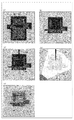
Images


Classifications
-
- H—ELECTRICITY
- H01—ELECTRIC ELEMENTS
- H01J—ELECTRIC DISCHARGE TUBES OR DISCHARGE LAMPS
- H01J37/00—Discharge tubes with provision for introducing objects or material to be exposed to the discharge, e.g. for the purpose of examination or processing thereof
- H01J37/30—Electron-beam or ion-beam tubes for localised treatment of objects
- H01J37/317—Electron-beam or ion-beam tubes for localised treatment of objects for changing properties of the objects or for applying thin layers thereon, e.g. for ion implantation
- H01J37/3178—Electron-beam or ion-beam tubes for localised treatment of objects for changing properties of the objects or for applying thin layers thereon, e.g. for ion implantation for applying thin layers on objects
-
- G—PHYSICS
- G01—MEASURING; TESTING
- G01N—INVESTIGATING OR ANALYSING MATERIALS BY DETERMINING THEIR CHEMICAL OR PHYSICAL PROPERTIES
- G01N1/00—Sampling; Preparing specimens for investigation
- G01N1/28—Preparing specimens for investigation including physical details of (bio-)chemical methods covered elsewhere, e.g. G01N33/50, C12Q
- G01N1/286—Preparing specimens for investigation including physical details of (bio-)chemical methods covered elsewhere, e.g. G01N33/50, C12Q involving mechanical work, e.g. chopping, disintegrating, compacting, homogenising
-
- H—ELECTRICITY
- H01—ELECTRIC ELEMENTS
- H01J—ELECTRIC DISCHARGE TUBES OR DISCHARGE LAMPS
- H01J37/00—Discharge tubes with provision for introducing objects or material to be exposed to the discharge, e.g. for the purpose of examination or processing thereof
- H01J37/26—Electron or ion microscopes; Electron or ion diffraction tubes
- H01J37/28—Electron or ion microscopes; Electron or ion diffraction tubes with scanning beams
-
- H—ELECTRICITY
- H01—ELECTRIC ELEMENTS
- H01J—ELECTRIC DISCHARGE TUBES OR DISCHARGE LAMPS
- H01J37/00—Discharge tubes with provision for introducing objects or material to be exposed to the discharge, e.g. for the purpose of examination or processing thereof
- H01J37/30—Electron-beam or ion-beam tubes for localised treatment of objects
- H01J37/3002—Details
- H01J37/3005—Observing the objects or the point of impact on the object
-
- H—ELECTRICITY
- H01—ELECTRIC ELEMENTS
- H01J—ELECTRIC DISCHARGE TUBES OR DISCHARGE LAMPS
- H01J37/00—Discharge tubes with provision for introducing objects or material to be exposed to the discharge, e.g. for the purpose of examination or processing thereof
- H01J37/30—Electron-beam or ion-beam tubes for localised treatment of objects
- H01J37/3002—Details
- H01J37/3007—Electron or ion-optical systems
-
- H—ELECTRICITY
- H01—ELECTRIC ELEMENTS
- H01J—ELECTRIC DISCHARGE TUBES OR DISCHARGE LAMPS
- H01J37/00—Discharge tubes with provision for introducing objects or material to be exposed to the discharge, e.g. for the purpose of examination or processing thereof
- H01J37/30—Electron-beam or ion-beam tubes for localised treatment of objects
- H01J37/31—Electron-beam or ion-beam tubes for localised treatment of objects for cutting or drilling
-
- G—PHYSICS
- G01—MEASURING; TESTING
- G01N—INVESTIGATING OR ANALYSING MATERIALS BY DETERMINING THEIR CHEMICAL OR PHYSICAL PROPERTIES
- G01N1/00—Sampling; Preparing specimens for investigation
- G01N1/28—Preparing specimens for investigation including physical details of (bio-)chemical methods covered elsewhere, e.g. G01N33/50, C12Q
- G01N1/286—Preparing specimens for investigation including physical details of (bio-)chemical methods covered elsewhere, e.g. G01N33/50, C12Q involving mechanical work, e.g. chopping, disintegrating, compacting, homogenising
- G01N2001/2873—Cutting or cleaving
-
- H—ELECTRICITY
- H01—ELECTRIC ELEMENTS
- H01J—ELECTRIC DISCHARGE TUBES OR DISCHARGE LAMPS
- H01J2237/00—Discharge tubes exposing object to beam, e.g. for analysis treatment, etching, imaging
- H01J2237/06—Sources
- H01J2237/063—Electron sources
-
- H—ELECTRICITY
- H01—ELECTRIC ELEMENTS
- H01J—ELECTRIC DISCHARGE TUBES OR DISCHARGE LAMPS
- H01J2237/00—Discharge tubes exposing object to beam, e.g. for analysis treatment, etching, imaging
- H01J2237/06—Sources
- H01J2237/08—Ion sources
-
- H—ELECTRICITY
- H01—ELECTRIC ELEMENTS
- H01J—ELECTRIC DISCHARGE TUBES OR DISCHARGE LAMPS
- H01J2237/00—Discharge tubes exposing object to beam, e.g. for analysis treatment, etching, imaging
- H01J2237/20—Positioning, supporting, modifying or maintaining the physical state of objects being observed or treated
- H01J2237/208—Elements or methods for movement independent of sample stage for influencing or moving or contacting or transferring the sample or parts thereof, e.g. prober needles or transfer needles in FIB/SEM systems
-
- H—ELECTRICITY
- H01—ELECTRIC ELEMENTS
- H01J—ELECTRIC DISCHARGE TUBES OR DISCHARGE LAMPS
- H01J2237/00—Discharge tubes exposing object to beam, e.g. for analysis treatment, etching, imaging
- H01J2237/245—Detection characterised by the variable being measured
- H01J2237/24564—Measurements of electric or magnetic variables, e.g. voltage, current, frequency
-
- H—ELECTRICITY
- H01—ELECTRIC ELEMENTS
- H01J—ELECTRIC DISCHARGE TUBES OR DISCHARGE LAMPS
- H01J2237/00—Discharge tubes exposing object to beam, e.g. for analysis treatment, etching, imaging
- H01J2237/26—Electron or ion microscopes
- H01J2237/28—Scanning microscopes
- H01J2237/2813—Scanning microscopes characterised by the application
- H01J2237/2817—Pattern inspection
-
- H—ELECTRICITY
- H01—ELECTRIC ELEMENTS
- H01J—ELECTRIC DISCHARGE TUBES OR DISCHARGE LAMPS
- H01J2237/00—Discharge tubes exposing object to beam, e.g. for analysis treatment, etching, imaging
- H01J2237/30—Electron or ion beam tubes for processing objects
- H01J2237/304—Controlling tubes
-
- H—ELECTRICITY
- H01—ELECTRIC ELEMENTS
- H01J—ELECTRIC DISCHARGE TUBES OR DISCHARGE LAMPS
- H01J2237/00—Discharge tubes exposing object to beam, e.g. for analysis treatment, etching, imaging
- H01J2237/30—Electron or ion beam tubes for processing objects
- H01J2237/317—Processing objects on a microscale
- H01J2237/3174—Etching microareas
- H01J2237/31742—Etching microareas for repairing masks
- H01J2237/31744—Etching microareas for repairing masks introducing gas in vicinity of workpiece
-
- H—ELECTRICITY
- H01—ELECTRIC ELEMENTS
- H01J—ELECTRIC DISCHARGE TUBES OR DISCHARGE LAMPS
- H01J2237/00—Discharge tubes exposing object to beam, e.g. for analysis treatment, etching, imaging
- H01J2237/30—Electron or ion beam tubes for processing objects
- H01J2237/317—Processing objects on a microscale
- H01J2237/3174—Etching microareas
- H01J2237/31745—Etching microareas for preparing specimen to be viewed in microscopes or analyzed in microanalysers
-
- H—ELECTRICITY
- H01—ELECTRIC ELEMENTS
- H01J—ELECTRIC DISCHARGE TUBES OR DISCHARGE LAMPS
- H01J2237/00—Discharge tubes exposing object to beam, e.g. for analysis treatment, etching, imaging
- H01J2237/30—Electron or ion beam tubes for processing objects
- H01J2237/317—Processing objects on a microscale
- H01J2237/31749—Focused ion beam
Definitions
- the present invention relates to a charged particle beam apparatus having a function of automatically preparing a sample for electron microscope observation using a charged particle beam and a sample preparation method.
- Patent Document 1 A technique related to a charged particle beam apparatus, particularly a focused ion beam (FIB) apparatus, is disclosed in Patent Document 1.
- the FIB apparatus can perform microfabrication of a sample by utilizing a sputtering phenomenon that occurs when the sample is irradiated with a focused ion beam.
- Patent Document 2 discloses a technique related to a combination of an FIB apparatus and an SEM or STEM.
- the FIB irradiation axis and the electron beam irradiation axis are arranged at an acute angle, and a sample is installed at the intersection.
- a section subjected to FIB processing can be observed with an SEM as it is.
- a desired region is extracted from a sample in a FIB processing apparatus, and is used for observation of a transmission electron microscope (TEM) or a scanning transmission electron microscope (STEM).
- TEM transmission electron microscope
- STEM scanning transmission electron microscope
- a microsampling method capable of producing a thin film sample is disclosed. This method comprises the steps of conductive film deposition, peripheral processing, bottom cutting, mechanical probe fixing, support cutting, micro sample extraction, fixing to a sample stage, mechanical probe cutting, and thin film processing. Traditionally, the operator manually operated the entire process.
- the FIB processing method is a technique for irradiating a sample with a focused ion beam and performing fine processing using a sputtering phenomenon.
- FIB processing of insulating materials such as ceramics and polymers
- charges accumulate on the sample due to ion irradiation and are easily charged.
- a conductive material is coated on the entire surface of the sample to prevent charging.
- Such pretreatment is useful for detecting contact between the mechanical probe used in the microsampling method and the sample, in addition to preventing charging.
- An object of the present invention relates to providing a sample preparation method that eliminates the problem of contact detection that has conventionally relied on user experience and uses the above-described automatic processing.
- the present invention has the following configuration in view of the above problems.
- a charged particle beam apparatus comprising a possible probe, a gas nozzle that discharges a conductive gas to the sample, and a control unit that controls driving of the probe and gas emission from the gas nozzle
- the control unit includes: After processing the sample by irradiating the sample with a charged particle beam and before bringing the probe into contact with the sample, the gas is discharged from the gas nozzle toward the processing position, and the charged particle beam is irradiated to process the sample.
- a charged particle beam apparatus comprising a contact detection unit that forms a conductive film on a portion and determines that the conductive film formed on the processing portion is in contact with the probe.
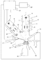
- the schematic diagram which showed the structure of the charged particle beam apparatus of one Example of this invention The schematic diagram which showed the structure of the charged particle beam apparatus of one Example of this invention.
- the schematic diagram which shows the procedure of the general microsampling method The schematic diagram which showed the contact detection method with the sample using a mechanical probe.
- the schematic diagram which shows one Example of electroconductive film film-forming on the sample surface by this invention The schematic diagram which shows one Example of electroconductive film film-forming on the sample surface by this invention.
- the schematic diagram which shows one Example of electroconductive film film-forming on the sample surface by this invention The schematic diagram which shows one Example of electroconductive film film-forming on the sample surface by this invention.
- the schematic diagram which shows one Example of electroconductive film film-forming on the surface and side surface of a micro sample in the case of fixing the bottom part of the micro sample extracted by this invention to a sample stand.
- the schematic diagram which shows one Example of electroconductive film film-forming on the surface of a micro sample, a side surface, and a bottom cut surface in the case of fixing the bottom part of the extracted micro sample by this invention to a sample stand.
- the schematic diagram which shows one Example of electroconductive film film-forming on the surface of a micro sample, a side surface, and a bottom part cut surface in the case of fixing the side surface of the extracted micro sample by this invention to a sample stand. It is an Example of electroconductive film film-forming on the sample surface by this invention. It is an Example of electroconductive film film-forming on the sample surface by this invention.
- the schematic diagram of the sample section structure which can apply the present invention. A procedure when the present invention is applied to automatic processing of a microsampling method.
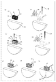
- FIG. 1 is a schematic diagram showing the configuration of a charged particle beam apparatus capable of observing an SEM image in the same chamber as the fine processing by FIB processing.
- the ion beam irradiation system 1 includes an ion source 2, a focusing lens 3, a deflector 4, and an objective lens 5.
- the ion beam irradiation system 1 has a function of forming an ion beam 6 and focusing and scanning the sample surface.
- the electron beam irradiation system 7 includes an electron source 8, a focusing lens 9, a deflector 10, and an objective lens 11, and has a function of forming an electron beam 12 and focusing and scanning on the sample surface.
- the original sample 13 is fixed on the sample stage 14.
- the chamber 15 includes an ion beam irradiation system 1, an electron beam irradiation system 7, a sample stage 14, a secondary charged particle detector 17 that detects secondary charged particles 16 generated by the ion beam 6 and electron beam 12 irradiation, and a micro sample.
- a mechanical probe 18 capable of extracting gas
- a deposition nozzle 19 capable of ejecting gas and forming a film
- a vacuum pump 20 They are controlled by the control unit 21.
- An optical system setting window and a secondary charged particle beam image are displayed on the CRT 22.
- On the sample stage 14, a sample stage for fixing the original sample 13 and a micro sample extracted using the mechanical probe 18 can be installed.
- the ion beam irradiation system 1 and the electron beam irradiation system 7 can scan the same location on the original sample 13 or the micro sample.
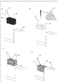
- FIG. 2 is a schematic diagram showing a configuration of a charged particle beam apparatus capable of fine processing by FIB processing.
- the ion beam irradiation system 1 includes an ion source 2, a focusing lens 3, a deflector 4, and an objective lens 5.
- the ion beam irradiation system 1 has a function of forming an ion beam 6 and focusing and scanning the sample surface.
- the original sample 13 is fixed on the sample stage 14.
- the chamber 15 includes an ion beam irradiation system 1, a sample stage 14, a secondary charged particle detector 17 that detects secondary charged particles 16 generated by the ion beam 6 irradiation, a mechanical probe 18 that can extract a minute sample, and gas.
- a deposition nozzle 19 and a vacuum pump 20 capable of jetting film formation are provided. They are controlled by the control unit 21.
- An optical system setting window and a secondary charged particle beam image are displayed on the CRT 22.
- the ion beam irradiation system can scan the original sample 13 and the micro sample.
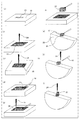
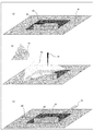
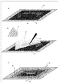
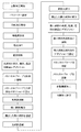
- FIG. 3 shows a procedure of a general microsampling method.
- the original sample 13 is inserted into the charged particle beam apparatus, and a conductive film 23 is formed on the surface of the original sample 13 by the deposition function ((a) of FIG. 3).
- peripheral processing is performed with the FIB 24 leaving the conductive film 23 ((b) of FIG. 3).
- the sample is tilted and the bottom 25 is cut with the FIB 24 ((c) of FIG. 3). Return the sample tilt to the original angle.
- the mechanical probe 18 is brought into contact with the sample surface.
- the conductive film 23 is formed using the deposition function, and the mechanical probe and the sample are fixed ((d) in FIG. 3).
- the support part 26 is cut off by the FIB 24 ((e) of FIG. 3).
- the micro sample 27 is extracted ((f) in FIG. 3).
- the extracted micro sample 27 is brought into contact with the sample stage 28.
- the conductive film 23 is formed by the deposition function, and the micro sample 27 and the sample stage 28 are fixed ((g) in FIG. 3).
- the mechanical probe 18 is cut by the FIB 24 ((h) in FIG. 3).
- a thin sample is processed into a thin film using the FIB 24 to produce a thin film sample 29 ((i) in FIG. 3).
- conductive film deposition FIG. 3 (a)
- sample extraction FIG. 3 (f)
- thin film processing FIG. 3 (i)
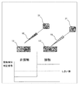
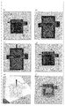
- FIG. 4 shows a method for detecting contact with a sample using a mechanical probe.
- the mechanical probe 18 is connected to the contact detection determination unit 31.
- the contact detection determination unit 31 can read a contact detection determination signal between the sample 13 and the mechanical probe 18. When the contact detection determination signal is equal to or less than the threshold value, it is determined to be non-contact, and when the contact detection determination signal is equal to or greater than the threshold value, it is determined to be contact.
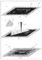
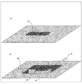
- 5 and 6 show examples of forming a conductive film on the surface of a sample according to the present invention. These embodiments can be implemented by any of the FIB apparatus, the FIB-SEM apparatus, and the FIB-STEM apparatus.
- a conductive material is coated on the entire surface of the sample. This is to operate the antistatic function and the contact detection function between the mechanical probe and the sample. After coating, a sample is inserted into the charged particle beam apparatus. First, a conductive film is formed on the surface of the observation target region using the position function, peripheral processing, and bottom cutting are performed. These operations can be performed without being affected by charging because the conductive material 41 has already been coated (FIG. 5A).
- FIG. 5B shows a state in which a conductive film is formed while jetting a gas 45 from the deposition nozzle 19 and irradiating the FIB 24.
- the conductive film 23 is formed on the surface 43, and the electrical conduction path 46 between the mechanical probe 18 and the surface 43 can be secured, so that the contact detection operates normally ((c) in FIG. 5).
- FIG. 5B shows a state in which a conductive film is formed while jetting a gas 45 from the deposition nozzle 19 and irradiating the FIB 24.
- FIG. 6 shows an example of forming a conductive film on the surface of a sample according to the present invention.
- the observation direction in each figure was the FIB incident direction.
- FIG. 5 it is assumed that the sputtered material 42 generated by the peripheral processing is reattached to the surface 43 and the side surface 44 ((a) of FIG. 6).
- the sample is tilted ((b) in FIG. 6).
- the scale is reduced in the vertical direction because the sample is observed in an inclined state.
- the bottom 25 is cut with the FIB 24 ((c) in FIG. 6). Next, it deposits on the surface 43, the side surface 44, and the bottom part cut surface 51 of a process site
- 6D shows a state in which the conductive film is formed while the gas 45 is ejected from the deposition nozzle 19 and irradiated with the FIB 24.
- the deposition may be performed in a state of being further inclined from the angle at which the bottom is cut.
- the conductive film 23 is formed on the surface 43, the side surface 44, and the bottom cut surface 51, and an electrical conduction path between the mechanical probe and the sample surface can be secured, so that the contact detection operates normally (see FIG. 6 (e)).
- 7 and 8 show an embodiment of forming a conductive film on the sample surface according to the present invention.
- FIB apparatus can be implemented by any of the FIB apparatus, the FIB-SEM apparatus, and the FIB-STEM apparatus.
- the FIB beam intensity follows the Gaussian distribution and is strongest at the center and weaker at the periphery.
- the surface is slightly sputtered due to the influence of a part having a low beam intensity (beam flare).
- beam flare the beam intensity
- FIG. 7B shows a state where a conductive film is formed while jetting gas 45 from the deposition nozzle 19 and scanning with the FIB 24. By this treatment, the conductive film 23 is formed, and the electrical conduction path 46 between the mechanical probe 18 and the surface 43 can be secured ((c) in FIG. 7).
- the conductive film 23 may be formed on the support portion in advance during the deposition at the start of microsampling ((a) of FIG. 8). It is desirable that the thickness of the conductive film at this time is adjusted to be a little thick so as not to disappear due to beam flare. By this processing, the conductive film 23 on the upper portion of the support portion does not disappear even if peripheral processing is performed, so that an electrical conduction path 46 between the mechanical probe 18 and the surface 43 can be secured ((b) of FIG. 8).
- the micro sample to which the mechanical probe is fixed is extracted and fixed on the sample stage after the support portion is cut. Detection of contact with the mechanical probe, the extracted microsample, and the sample stage is performed by detecting electrical continuity therebetween.
- the sample is an insulating material or when a sputtered material is attached, there is a problem that electrical continuity cannot be secured and contact detection does not operate normally.
- 9, 10 and 11 show examples of forming a conductive film on a sample according to the present invention. These embodiments can be implemented by any of the FIB apparatus, the FIB-SEM apparatus, and the FIB-STEM apparatus.
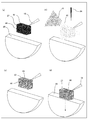
- FIG. 9 shows an embodiment of forming a conductive film on the surface and side surfaces of a micro sample when the bottom of the extracted micro sample is fixed to a sample stage.
- FIG. 9A is a schematic diagram before the micro sample 27 extracted by the mechanical probe 18 is brought into contact with the sample stage 28. Next, it deposits on the surface 43 and the side surface 44 of the micro sample 27.
- FIG. 9B shows a state in which a conductive film is formed while ejecting the gas 45 from the deposition nozzle 19 and irradiating the FIB 24.
- the conductive film 23 is formed on the surface 43 and the side surface 44 ((c) of FIG. 9), and an electrical conduction path 46 between the mechanical probe 18, the micro sample 27, and the sample stage 28 can be secured, so that contact is made.
- FIG. 10 shows an example of forming a conductive film on the surface, side surface, and bottom cut surface of the micro sample when the bottom of the extracted micro sample is fixed to the sample stage.
- FIG. 10A is a schematic diagram before the micro sample 27 extracted by the mechanical probe 18 is brought into contact with the sample stage 28. In this state, it is deposited on the surface 43 and the side surface 44 of the micro sample 27.
- FIG. 10B shows a state in which a conductive film is formed while jetting a gas 45 from the deposition nozzle 19 and irradiating the FIB 24.
- FIG. 10 shows an example of forming a conductive film on the surface, side surface, and bottom cut surface of the micro sample when the bottom of the extracted micro sample is fixed to the sample stage.
- FIG. 10A is a schematic diagram before the micro sample 27 extracted by the mechanical probe 18 is brought into contact with the sample stage 28. In this state, it is deposited on the surface 43 and the side surface 44 of the micro sample 27.
- FIG. 10B shows a
- FIG. 10C is a schematic view after the micro sample 27 is rotated in the ⁇ direction by using the rotating mechanism of the mechanical probe 18 after the conductive film 23 is formed on the surface 43 and the side surface 44. Next, in this state, it is deposited on the bottom cut surface 51 of the micro sample 27.
- FIG. 10D shows a state in which a conductive film is formed on the bottom cut surface in a sample state where the side and bottom cut surfaces can be expected from the FIB 24 while the gas 45 is ejected from the deposition nozzle 19 and irradiated with the FIB 24. Indicates.
- the conductive film 23 is also formed in the bottom cut portion 51 ((e) in FIG. 10).
- FIG. 11 shows an example of forming a conductive film on the surface, side, and bottom of the micro sample when the side surface of the extracted micro sample is fixed to the sample stage.
- FIG. 11A is a schematic diagram before the micro sample 27 extracted by the mechanical probe 18 is brought into contact with the sample stage 28. Next, the surface 43 and the side surface 44 are deposited.
- FIG. 11B shows a state in which the conductive film is formed while the gas 45 is ejected from the deposition nozzle 19 and irradiated with the FIB 24.
- the conductive film 23 is formed on the surface 43 and the side surface 44 ((c) of FIG. 11), and the electrical conduction path 46 of the mechanical probe 18, the minute sample 27, and the sample stage 28 can be secured, so that contact detection is possible. It will operate normally ((d) of FIG. 11).
- a conductive film is formed by depositing on the surface and side surfaces of a minute sample.
- the micro sample is rotated using the rotating mechanism of the mechanical probe, and the side and bottom cut surfaces are deposited on the bottom cut surface in a sample state that can be expected from the FIB, and a conductive film is formed.
- FIGS. 5 to 11 are embodiments relating to the formation of a conductive film by FIB, and therefore any of the FIB apparatus, FIB-SEM apparatus, and FIB-STEM apparatus can be implemented.
- the formation of the conductive film using the electron beam can be performed only by the FIB-SEM apparatus or the FIB-STEM apparatus. That is, in the embodiments shown in FIGS. 5 to 11, the same processing can be performed using an electron beam instead of the FIB used for forming the conductive film.
- FIG. 12 shows an example of forming a conductive film on the sample surface according to the present invention.
- the sputtered material 42 is reattached to the surface 43 and the side surface 44 ((a) of FIG. 12). Since the processing site is electrically isolated, there is a problem that electrical continuity between the mechanical probe and the sample cannot be ensured and contact detection is impossible. Therefore, a conductive film is formed on the surface using the deposition function ((b) of FIG. 12).
- FIG. 12B shows a state where a gas 45 is ejected from the deposition nozzle 19 and a conductive film is formed on the surface 43 while scanning with the electron beam 12.
- the conductive film 23 is formed on the surface 43 and the electrical conduction path 46 between the mechanical probe 18 and the surface 43 can be secured, so that the contact detection operates normally ((c) in FIG. 12).
- FIG. 13 shows an example of forming a conductive film on the surface of a sample according to the present invention. The observation direction in each figure was the incident direction of the electron beam. Similarly to FIG. 12, it is assumed that the sputtered material 42 generated by the peripheral processing is reattached to the surface 43 and the side surface 44 ((a) of FIG. 13). The sample is tilted (FIG.
- FIG. 13B shows a state in which a conductive film is formed while jetting a gas 45 from the deposition nozzle 19 and scanning with the electron beam 12.
- the deposition may be performed after adjusting the angle so that the bottom cut surface can be observed with an electron beam.
- FIG. 14 shows a schematic diagram of a cross-sectional structure of a sample to which the present invention can be applied.
- the present invention is applicable to a sample in which an electrical conduction path cannot be ensured, such as a sample including a part of an insulating material in an insulating material or a conductive material. It can also be used for conductive materials.
- FIG. 14A is a schematic cross-sectional view of an insulating material.
- Insulating materials include various materials such as ceramics, polymers, and biological samples.
- ceramics is shown as a representative example.
- the ceramic 140 has a sintered body structure of a large number of grains 141.
- FIG. 14B is a schematic cross-sectional view of a sample that partially includes an insulating material in the conductive material.
- a semiconductor example is shown as a representative example.
- the semiconductor 142 has a structure in which an insulating film 144 and a conductive film 145 are stacked over a Si substrate 143 that is a conductive material.
- FIGS. 5 to 14 can be applied to the automatic processing and manual operation of the microsampling method.
- FIG. 15 shows a processing procedure when the present invention is applied to automatic processing of the microsampling method.
- machining Conducting conductive film formation by deposition, peripheral processing, and bottom cutting.
- a conductive film is formed by depositing on the surface, side surface, and bottom cut surface.
- Insert the mechanical probe A mechanical probe is brought into contact with the sample surface. An electrical conduction path is secured and contact detection is activated.
- the tip and the original sample are fixed by deposition. Cut the support with FIB. Remove a small sample and retract it along with the mechanical probe. Evacuate the original sample. Insert the sample stage. Insert the excised microsample.
- the conductive film is deposited by depositing on the surface, side surface, and bottom cut surface of the extracted micro sample.
- a minute sample is brought into contact with the sample table.
- An electrical conduction path is secured and contact detection is activated.
- a micro sample and a sample stage are fixed by deposition. Cut the mechanical probe with FIB. Retract the mechanical probe.
- automatic thin film processing is performed to produce a thin film sample.
- the cross-sectional SEM observation is intended, the cross-section may be simply finished with FIB.
Landscapes
- Chemical & Material Sciences (AREA)
- Analytical Chemistry (AREA)
- Physics & Mathematics (AREA)
- General Health & Medical Sciences (AREA)
- Life Sciences & Earth Sciences (AREA)
- Biochemistry (AREA)
- Health & Medical Sciences (AREA)
- General Physics & Mathematics (AREA)
- Immunology (AREA)
- Pathology (AREA)
- Engineering & Computer Science (AREA)
- Plasma & Fusion (AREA)
- Sampling And Sample Adjustment (AREA)
Priority Applications (3)
| Application Number | Priority Date | Filing Date | Title |
|---|---|---|---|
| US14/434,687 US9362088B2 (en) | 2012-10-15 | 2013-10-09 | Charged particle beam device and sample preparation method |
| CN201380053492.4A CN104737266B (zh) | 2012-10-15 | 2013-10-09 | 带电粒子束装置以及试样制作方法 |
| DE112013004612.1T DE112013004612B4 (de) | 2012-10-15 | 2013-10-09 | Mit einem Strahl geladener Teilchen arbeitende Vorrichtung und Probenpräparationsverfahren |
Applications Claiming Priority (2)
| Application Number | Priority Date | Filing Date | Title |
|---|---|---|---|
| JP2012-227596 | 2012-10-15 | ||
| JP2012227596A JP5887247B2 (ja) | 2012-10-15 | 2012-10-15 | 荷電粒子線装置および試料作製法 |
Publications (1)
| Publication Number | Publication Date |
|---|---|
| WO2014061524A1 true WO2014061524A1 (ja) | 2014-04-24 |
Family
ID=50488092
Family Applications (1)
| Application Number | Title | Priority Date | Filing Date |
|---|---|---|---|
| PCT/JP2013/077453 Ceased WO2014061524A1 (ja) | 2012-10-15 | 2013-10-09 | 荷電粒子線装置および試料作製法 |
Country Status (5)
| Country | Link |
|---|---|
| US (1) | US9362088B2 (enExample) |
| JP (1) | JP5887247B2 (enExample) |
| CN (1) | CN104737266B (enExample) |
| DE (1) | DE112013004612B4 (enExample) |
| WO (1) | WO2014061524A1 (enExample) |
Families Citing this family (9)
| Publication number | Priority date | Publication date | Assignee | Title |
|---|---|---|---|---|
| KR102383571B1 (ko) * | 2014-06-30 | 2022-04-06 | 가부시키가이샤 히다치 하이테크 사이언스 | 자동 시료 제작 장치 |
| JP6231461B2 (ja) * | 2014-10-31 | 2017-11-15 | アオイ電子株式会社 | 試料固定装置 |
| JP6689602B2 (ja) | 2014-12-22 | 2020-04-28 | カール ツァイス マイクロスコーピー エルエルシー | 荷電粒子ビームシステム及び方法 |
| CN105158516B (zh) * | 2015-08-20 | 2018-10-16 | 上海华力微电子有限公司 | 一种集成电路分析中透射电镜平面样品的制备方法 |
| CN106226134A (zh) * | 2016-07-29 | 2016-12-14 | 上海华力微电子有限公司 | 制备透射电子显微镜样品的方法 |
| JP6885576B2 (ja) * | 2017-01-19 | 2021-06-16 | 株式会社日立ハイテクサイエンス | 荷電粒子ビーム装置 |
| JP6931214B2 (ja) * | 2017-01-19 | 2021-09-01 | 株式会社日立ハイテクサイエンス | 荷電粒子ビーム装置 |
| JP6974820B2 (ja) * | 2017-03-27 | 2021-12-01 | 株式会社日立ハイテクサイエンス | 荷電粒子ビーム装置、試料加工方法 |
| US11315754B2 (en) * | 2020-04-27 | 2022-04-26 | Applied Materials Israel Ltd. | Adaptive geometry for optimal focused ion beam etching |
Citations (4)
| Publication number | Priority date | Publication date | Assignee | Title |
|---|---|---|---|---|
| JP2001235321A (ja) * | 1999-12-13 | 2001-08-31 | Mitsubishi Electric Corp | 集束イオンビーム装置,集束イオンビーム装置の制御方法及び接触検出方法 |
| JP2004245660A (ja) * | 2003-02-13 | 2004-09-02 | Seiko Instruments Inc | 小片試料の作製とその壁面の観察方法及びそのシステム |
| JP2009224788A (ja) * | 2009-04-27 | 2009-10-01 | Hitachi Ltd | プローブ装置 |
| JP2010507882A (ja) * | 2006-10-20 | 2010-03-11 | エフ・イ−・アイ・カンパニー | サンプル抽出および取り扱いのための方法および装置 |
Family Cites Families (11)
| Publication number | Priority date | Publication date | Assignee | Title |
|---|---|---|---|---|
| JP2774884B2 (ja) | 1991-08-22 | 1998-07-09 | 株式会社日立製作所 | 試料の分離方法及びこの分離方法で得た分離試料の分析方法 |
| JPH0582479A (ja) | 1991-09-19 | 1993-04-02 | Hitachi Ltd | 集束イオンビーム装置 |
| EP0927880A4 (en) * | 1997-07-22 | 2010-11-17 | Hitachi Ltd | METHOD AND DEVICE FOR PREPARING SAMPLES |
| JP3401426B2 (ja) | 1998-03-23 | 2003-04-28 | 日本電子株式会社 | Fib−sem装置における試料加工方法およびfib−sem装置 |
| US6452174B1 (en) * | 1999-12-13 | 2002-09-17 | Mitsubishi Denki Kabushiki Kaisha | Charged particle beam apparatus and method of controlling same |
| JP4408538B2 (ja) * | 2000-07-24 | 2010-02-03 | 株式会社日立製作所 | プローブ装置 |
| JP4088533B2 (ja) * | 2003-01-08 | 2008-05-21 | 株式会社日立ハイテクノロジーズ | 試料作製装置および試料作製方法 |
| US7112790B1 (en) * | 2003-08-13 | 2006-09-26 | Cypress Semiconductor Corp. | Method to prepare TEM samples |
| EP2106555B1 (en) * | 2006-10-20 | 2015-01-07 | FEI Company | Method for s/tem sample analysis |
| DE102009008166A1 (de) * | 2009-02-10 | 2010-09-02 | Carl Zeiss Nts Gmbh | Verfahren zur Abscheidung von Schutzstrukturen |
| CN202189227U (zh) * | 2011-07-26 | 2012-04-11 | 中国科学院物理研究所 | 纳米图形化和超宽频电磁特性测量系统 |
-
2012
- 2012-10-15 JP JP2012227596A patent/JP5887247B2/ja active Active
-
2013
- 2013-10-09 US US14/434,687 patent/US9362088B2/en active Active
- 2013-10-09 DE DE112013004612.1T patent/DE112013004612B4/de active Active
- 2013-10-09 CN CN201380053492.4A patent/CN104737266B/zh active Active
- 2013-10-09 WO PCT/JP2013/077453 patent/WO2014061524A1/ja not_active Ceased
Patent Citations (4)
| Publication number | Priority date | Publication date | Assignee | Title |
|---|---|---|---|---|
| JP2001235321A (ja) * | 1999-12-13 | 2001-08-31 | Mitsubishi Electric Corp | 集束イオンビーム装置,集束イオンビーム装置の制御方法及び接触検出方法 |
| JP2004245660A (ja) * | 2003-02-13 | 2004-09-02 | Seiko Instruments Inc | 小片試料の作製とその壁面の観察方法及びそのシステム |
| JP2010507882A (ja) * | 2006-10-20 | 2010-03-11 | エフ・イ−・アイ・カンパニー | サンプル抽出および取り扱いのための方法および装置 |
| JP2009224788A (ja) * | 2009-04-27 | 2009-10-01 | Hitachi Ltd | プローブ装置 |
Also Published As
| Publication number | Publication date |
|---|---|
| JP2014082028A (ja) | 2014-05-08 |
| DE112013004612B4 (de) | 2019-11-21 |
| CN104737266A (zh) | 2015-06-24 |
| US20150255250A1 (en) | 2015-09-10 |
| CN104737266B (zh) | 2016-10-26 |
| US9362088B2 (en) | 2016-06-07 |
| JP5887247B2 (ja) | 2016-03-16 |
| DE112013004612T5 (de) | 2015-07-02 |
Similar Documents
| Publication | Publication Date | Title |
|---|---|---|
| JP5887247B2 (ja) | 荷電粒子線装置および試料作製法 | |
| JP6224612B2 (ja) | 断面観察薄片の裏側薄化用の高スループットtem調製プロセスおよびハードウェア | |
| JP6366216B2 (ja) | Tem画像化用の薄い試料を作製する方法 | |
| JP5173142B2 (ja) | 試料作製のための反復的周状切削 | |
| US8642958B2 (en) | Composite charged particle beam apparatus and sample processing and observing method | |
| JP5350605B2 (ja) | サンプルの作製 | |
| JP5908964B2 (ja) | 複合集束イオンビーム装置 | |
| US9384941B2 (en) | Charged particle beam apparatus and sample observation method | |
| US20100243889A1 (en) | Forming an image while milling a work piece | |
| CN105103270A (zh) | 用于准备用于成像的样本的方法 | |
| TW201409525A (zh) | 用於聚焦離子束加工之端點檢測 | |
| US10347461B2 (en) | Method for the in situ preparation of microscopic specimens | |
| US20060017016A1 (en) | Method for the removal of a microscopic sample from a substrate | |
| JP5142240B2 (ja) | 荷電ビーム装置及び荷電ビーム加工方法 | |
| KR102485795B1 (ko) | 시료 트렌치 매립 방법 | |
| JP2010197272A (ja) | 電子顕微鏡の試料コーティング方法 | |
| EP3023763B1 (en) | Specimen preparation device | |
| JP5246981B2 (ja) | 試料加工方法及びイオンビーム装置 | |
| JP2019174204A (ja) | デポジション膜の形成方法 | |
| JP6305143B2 (ja) | 断面加工方法 |
Legal Events
| Date | Code | Title | Description |
|---|---|---|---|
| 121 | Ep: the epo has been informed by wipo that ep was designated in this application |
Ref document number: 13848022 Country of ref document: EP Kind code of ref document: A1 |
|
| DPE1 | Request for preliminary examination filed after expiration of 19th month from priority date (pct application filed from 20040101) | ||
| WWE | Wipo information: entry into national phase |
Ref document number: 112013004612 Country of ref document: DE Ref document number: 1120130046121 Country of ref document: DE |
|
| WWE | Wipo information: entry into national phase |
Ref document number: 14434687 Country of ref document: US |
|
| 122 | Ep: pct application non-entry in european phase |
Ref document number: 13848022 Country of ref document: EP Kind code of ref document: A1 |