WO2014057751A1 - 積層セラミック電子部品およびその製造方法 - Google Patents
積層セラミック電子部品およびその製造方法 Download PDFInfo
- Publication number
- WO2014057751A1 WO2014057751A1 PCT/JP2013/074061 JP2013074061W WO2014057751A1 WO 2014057751 A1 WO2014057751 A1 WO 2014057751A1 JP 2013074061 W JP2013074061 W JP 2013074061W WO 2014057751 A1 WO2014057751 A1 WO 2014057751A1
- Authority
- WO
- WIPO (PCT)
- Prior art keywords
- crystal phase
- multilayer ceramic
- external electrode
- area
- electronic component
- Prior art date
- Legal status (The legal status is an assumption and is not a legal conclusion. Google has not performed a legal analysis and makes no representation as to the accuracy of the status listed.)
- Ceased
Links
Images


Classifications
-
- H—ELECTRICITY
- H01—ELECTRIC ELEMENTS
- H01G—CAPACITORS; CAPACITORS, RECTIFIERS, DETECTORS, SWITCHING DEVICES, LIGHT-SENSITIVE OR TEMPERATURE-SENSITIVE DEVICES OF THE ELECTROLYTIC TYPE
- H01G4/00—Fixed capacitors; Processes of their manufacture
- H01G4/30—Stacked capacitors
-
- H—ELECTRICITY
- H01—ELECTRIC ELEMENTS
- H01G—CAPACITORS; CAPACITORS, RECTIFIERS, DETECTORS, SWITCHING DEVICES, LIGHT-SENSITIVE OR TEMPERATURE-SENSITIVE DEVICES OF THE ELECTROLYTIC TYPE
- H01G4/00—Fixed capacitors; Processes of their manufacture
- H01G4/002—Details
- H01G4/005—Electrodes
- H01G4/008—Selection of materials
-
- H—ELECTRICITY
- H01—ELECTRIC ELEMENTS
- H01G—CAPACITORS; CAPACITORS, RECTIFIERS, DETECTORS, SWITCHING DEVICES, LIGHT-SENSITIVE OR TEMPERATURE-SENSITIVE DEVICES OF THE ELECTROLYTIC TYPE
- H01G4/00—Fixed capacitors; Processes of their manufacture
- H01G4/002—Details
- H01G4/005—Electrodes
- H01G4/008—Selection of materials
- H01G4/0085—Fried electrodes
-
- H—ELECTRICITY
- H01—ELECTRIC ELEMENTS
- H01G—CAPACITORS; CAPACITORS, RECTIFIERS, DETECTORS, SWITCHING DEVICES, LIGHT-SENSITIVE OR TEMPERATURE-SENSITIVE DEVICES OF THE ELECTROLYTIC TYPE
- H01G4/00—Fixed capacitors; Processes of their manufacture
- H01G4/002—Details
- H01G4/005—Electrodes
- H01G4/012—Form of non-self-supporting electrodes
-
- H—ELECTRICITY
- H01—ELECTRIC ELEMENTS
- H01G—CAPACITORS; CAPACITORS, RECTIFIERS, DETECTORS, SWITCHING DEVICES, LIGHT-SENSITIVE OR TEMPERATURE-SENSITIVE DEVICES OF THE ELECTROLYTIC TYPE
- H01G4/00—Fixed capacitors; Processes of their manufacture
- H01G4/002—Details
- H01G4/018—Dielectrics
- H01G4/06—Solid dielectrics
- H01G4/08—Inorganic dielectrics
- H01G4/12—Ceramic dielectrics
- H01G4/1209—Ceramic dielectrics characterised by the ceramic dielectric material
-
- H—ELECTRICITY
- H01—ELECTRIC ELEMENTS
- H01G—CAPACITORS; CAPACITORS, RECTIFIERS, DETECTORS, SWITCHING DEVICES, LIGHT-SENSITIVE OR TEMPERATURE-SENSITIVE DEVICES OF THE ELECTROLYTIC TYPE
- H01G4/00—Fixed capacitors; Processes of their manufacture
- H01G4/002—Details
- H01G4/018—Dielectrics
- H01G4/06—Solid dielectrics
- H01G4/08—Inorganic dielectrics
- H01G4/12—Ceramic dielectrics
- H01G4/1209—Ceramic dielectrics characterised by the ceramic dielectric material
- H01G4/1218—Ceramic dielectrics characterised by the ceramic dielectric material based on titanium oxides or titanates
- H01G4/1227—Ceramic dielectrics characterised by the ceramic dielectric material based on titanium oxides or titanates based on alkaline earth titanates
-
- H—ELECTRICITY
- H01—ELECTRIC ELEMENTS
- H01G—CAPACITORS; CAPACITORS, RECTIFIERS, DETECTORS, SWITCHING DEVICES, LIGHT-SENSITIVE OR TEMPERATURE-SENSITIVE DEVICES OF THE ELECTROLYTIC TYPE
- H01G4/00—Fixed capacitors; Processes of their manufacture
- H01G4/002—Details
- H01G4/228—Terminals
- H01G4/232—Terminals electrically connecting two or more layers of a stacked or rolled capacitor
- H01G4/2325—Terminals electrically connecting two or more layers of a stacked or rolled capacitor characterised by the material of the terminals
-
- H—ELECTRICITY
- H01—ELECTRIC ELEMENTS
- H01G—CAPACITORS; CAPACITORS, RECTIFIERS, DETECTORS, SWITCHING DEVICES, LIGHT-SENSITIVE OR TEMPERATURE-SENSITIVE DEVICES OF THE ELECTROLYTIC TYPE
- H01G4/00—Fixed capacitors; Processes of their manufacture
- H01G4/002—Details
- H01G4/228—Terminals
- H01G4/248—Terminals the terminals embracing or surrounding the capacitive element, e.g. caps
Definitions
- the present invention relates to a multilayer ceramic electronic component such as a multilayer ceramic capacitor and a method for manufacturing the same, and more particularly, to an external electrode disposed on the surface of a multilayer ceramic element having an internal electrode so as to be electrically connected to the internal electrode. And a method for manufacturing the multilayer ceramic electronic component.
- a multilayer ceramic capacitor which is one of the typical multilayer ceramic electronic components, includes a multilayer ceramic element in which a plurality of internal electrodes are laminated via a ceramic layer, and a surface of the multilayer ceramic element so as to be electrically connected to the internal electrode. And an external electrode disposed on the surface.
- an external electrode of such a multilayer ceramic electronic component for example, a two-layer structure comprising a first layer in contact with the surface of a bare chip made of a ceramic sintered body and a second layer laminated on the first layer.
- a first layer is formed using a conductive paste in which a metal resinate is dispersed in an organic binder and an organic solvent
- a second layer is formed from a conductive paste in which a metal powder is dispersed in a thermosetting resin and an organic solvent.
- an external electrode that is in contact with the surface of a bare chip made of a ceramic sintered body and that is formed using a conductive paste in which a metal resinate is dispersed in an organic binder and an organic solvent is proposed. (See Patent Document 2).
- these external electrodes have good plating solution resistance when forming a plating layer, and electronic parts equipped with these external electrodes realize excellent electrical characteristics, reliability, and mechanical characteristics. It is supposed to be possible.
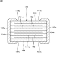
- the surface-mounted monolithic ceramic capacitor 130 generally includes a sintered monolithic ceramic element 133 in which a plurality of internal electrodes 131 a and 131 b are laminated via a ceramic layer 132. External electrodes 135a and 135b are disposed on both end surfaces 134a and 134b of the (ceramic capacitor element) so as to be electrically connected to the internal electrodes 131a and 131b.
- the external electrodes 135a and 135b are formed so as to wrap around the side surfaces 136 of the multilayer ceramic element 133 from both end surfaces 134a and 134b of the multilayer ceramic element 133.
- the rectangular parallelepiped ceramic body 133 has four side surfaces, and the external electrodes 135a and 135b wrap around the four side surfaces from both end surfaces 134a and 134b.
- the external electrodes 135a and 135b may be formed with a Ni plating film to prevent cracking during soldering (dissolution of the external electrode into the solder), and further to ensure solderability, In many cases, an Sn plating film is formed on the Ni plating film.
- the multilayer ceramic element 133 and the external electrode 135a are formed from the leading end portions (wrapping leading end portions) 144a and 144b of the surrounding portions of the external electrodes 135a and 135b. , 135b, the plating solution enters and the ceramic components are eluted.
- the strength of the multilayer ceramic element 133 in the vicinity of the wraparound tip portions 144a and 144b of the external electrodes 135a and 135b is reduced to cause cracks at the time of reflow, or the deflection strength is insufficient and the reliability is reduced. There is a problem of doing.
- the present invention solves the above-described problem, and does not cause a decrease in the strength of the multilayer ceramic element in the vicinity of the peripheral edge portion of the external electrode or a decrease in reliability due to the strength, and the highly reliable multilayer ceramic electronic
- An object is to provide a component and a method for manufacturing the component.
- the multilayer ceramic electronic component of the present invention is: A multilayer ceramic electronic component comprising a multilayer ceramic element having a structure in which an internal electrode and a ceramic layer are laminated, wherein an external electrode is disposed so as to be electrically connected to the internal electrode,
- the external electrode includes an inorganic material containing at least Si;
- a crystal phase containing at least Si, Ti, and Ba is formed at an interface with the ceramic layer constituting the multilayer ceramic element at a peripheral edge of the external electrode; and
- the following crystal phase area ratio value indicating the relationship between the area of the crystal phase formed at the interface with the ceramic layer and the area of the glass phase is 75 to 98. It is characterized by being in the range of%.
- Crystal phase area ratio (%) ⁇ Crystal phase area / (Crystal phase area + Glass phase area) ⁇ ⁇ 100
- the method for manufacturing the multilayer ceramic electronic component of the present invention includes: A method for producing a multilayer ceramic electronic component comprising a multilayer ceramic element having a structure in which an internal electrode and a ceramic layer are laminated, wherein an external electrode is disposed so as to be electrically connected to the internal electrode, A conductive paste for forming an external electrode containing at least Si is applied to the multilayer ceramic element so that Si, Ti, and Ba exist at the interface between the multilayer ceramic element and the conductive paste.
- Process Forming the external electrode by baking the conductive paste; In an atmosphere of oxygen electromotive force of 650 to 850 mV, heat treatment is performed under the conditions of a top temperature of 850 to 1000 ° C.
- Crystal phase area ratio (%) ⁇ Crystal phase area / (Crystal phase area + Glass phase area) ⁇ ⁇ 100
- the external electrode includes an inorganic substance containing at least Si, and at least at the interface between the peripheral edge of the external electrode and the ceramic layer constituting the multilayer ceramic element.
- the crystal phase containing Ti, Ti, and Ba is formed, and the relationship between the area of the crystal phase formed at the interface with the ceramic layer and the area of the glass phase in a region within 5 ⁇ m from the peripheral edge of the external electrode is shown. Since the value of the crystal phase area ratio is in the range of 75 to 98%, when a plating film is formed on the surface of the external electrode, the plating solution constitutes the peripheral edge portion of the external electrode and the multilayer ceramic element.
- the manufacturing method of the multilayer ceramic electronic component according to the present invention includes forming the external electrode by baking the conductive paste, and then performing the heat treatment under the above-described predetermined conditions to thereby obtain the peripheral edge portion of the external electrode.
- a crystal phase containing at least Si, Ti, and Ba is generated at the interface with the ceramic layer constituting the multilayer ceramic element, and the crystal phase area and glass in a region within 5 ⁇ m from the peripheral edge of the external electrode Since the crystal phase is generated so that the crystal phase area ratio indicating the relationship with the area of the phase is in the range of 75 to 98%, the plating solution can be used even when the plating film is formed on the surface of the external electrode.
- FIG. 1 is a perspective view schematically showing a configuration of a multilayer ceramic electronic component according to an embodiment of the present invention. It is sectional drawing which shows typically the structure of the multilayer ceramic electronic component concerning one Embodiment of this invention. It is sectional drawing which shows the structure of a common multilayer ceramic electronic component (multilayer ceramic capacitor).
- FIG. 1 is a perspective view showing a multilayer ceramic electronic component (here, a multilayer ceramic capacitor) according to an embodiment of the present invention
- FIG. 2 is a cross-sectional view taken along line AA of FIG.
- the multilayer ceramic capacitor 30 includes a sintered multilayer ceramic element 33 (ceramic capacitor element) in which a plurality of internal electrodes 31 a and 31 b are stacked via a ceramic layer 32.
- a sintered multilayer ceramic element 33 ceramic capacitor element
- one end sides of the internal electrodes 31 a and 31 b are alternately drawn out from both end faces 34 a and 34 b of the multilayer ceramic element 33.
- a pair of external electrodes 35a and 35b are disposed on both end faces 34a and 34b of the multilayer ceramic element 33 so as to be electrically connected to the internal electrodes 31a and 31b.
- the external electrodes 35 a and 35 b are formed so as to wrap around the side surface 36 of the multilayer ceramic element 33 from both end faces 34 a and 34 b of the multilayer ceramic element 33.
- the rectangular parallelepiped ceramic body 33 includes four side surfaces 36, and the external electrodes 35a and 35b wrap around the four side surfaces 36 from both end surfaces 34a and 34b.
- the interface between the tip portions (peripheral end portions) 44a and 44b of the wraparound portions of the external electrodes 35a and 35b and the ceramic layer 32 constituting the multilayer ceramic element 33 is schematically shown in FIG.
- the crystal phase C containing at least Si, Ti, and Ba and the glass phase G are configured to exist at a predetermined ratio.
- Crystal phase area ratio (Crystal phase area ratio (%) ⁇ Crystal phase area / (Crystal phase area + Glass phase area) ⁇ showing the relationship between the area of the crystal phase C formed at the interface and the area of the glass phase G X100) is in the range of 75 to 98%.
- the ceramic layer 32 is formed of a dielectric ceramic having a perovskite structure mainly composed of Ba and Ti, and the internal electrodes 31a and 31b are base metal electrodes made of Ni. is there.
- the external electrodes 35a and 35b are Cu baking electrode layers formed by applying and baking a conductive paste containing Cu powder as a conductive component and blending glass frit and the like.
- Ni plating films 36a and 36b are formed on the external electrodes 35a and 35b, and Sn plating films 37a and 37b are further formed on the Ni plating films 36a and 36b.
- an organic binder, an organic solvent, a plasticizer, and a dispersant are blended in a predetermined ratio to a ceramic dielectric powder made of a perovskite type compound containing Ba and Ti to prepare a ceramic slurry. .
- the ceramic slurry is formed on a resin film so that the thickness after drying becomes 4.0 ⁇ m, and a ceramic green sheet is produced.
- the conductive component (metal component) used in the conductive paste for forming the internal electrode there are no particular restrictions on the conductive component (metal component) used in the conductive paste for forming the internal electrode, but a material using Ni, Ni alloy, Cu, Cu alloy or the like, which is a base metal powder, may be used as appropriate. it can.
- a material using Ni, Ni alloy, Cu, Cu alloy or the like, which is a base metal powder may be used as appropriate. it can.
- 50 parts by weight of Ni powder having an average particle size of 0.3 ⁇ m, 45 parts by weight of a resin solution obtained by dissolving 10 parts by weight of ethyl cellulose in butyl carbitol, and the remaining dispersant and thickener are blended.
- a conductive paste was used.
- the divided multilayer ceramic elements are degreased in a nitrogen atmosphere at 400 ° C. for 10 hours, and then in a nitrogen-hydrogen-water vapor mixed atmosphere at a top temperature of 1200 ° C. and an oxygen partial pressure of 10 ⁇ . Firing is performed under conditions of 9 to 10 ⁇ 10 MPa.
- an external electrode (Cu-baked electrode layer) is formed by firing in a nitrogen-air-water vapor mixed atmosphere or a nitrogen-hydrogen-water vapor mixed atmosphere at a top temperature of 800 ° C. and an oxygen electromotive force of 280 mV. To do.
- test numbers 1 and 2 in Table 1 are samples of comparative examples in which the heat treatment conditions do not satisfy the requirements of the present invention.
- Test numbers 3 to 8 are examples of the examples in which the heat treatment conditions satisfy the requirements of the present invention. It is a sample.
- the location determined to be a crystal phase was cut out by FIB processing, spot diffraction was performed using TEM (Transmission Electron Microscope), and it was confirmed that there was a crystal peak.
- TEM Transmission Electron Microscope
- spot diffraction was performed using TEM, and it was confirmed that there was no crystal peak.
- Crystal phase area ratio (%) ⁇ Crystal phase area / (Crystal phase area + Glass phase area) ⁇ ⁇ 100 The results are also shown in Table 1.
- the crystal phase was a crystal phase containing at least Si, Ba, and Ti. Since this crystal phase does not elute into the Ni plating solution, an increase in the crystal phase results in an improvement in the Ni plating solution resistance at the tip (periphery end) of the wraparound portion of the external electrode, resulting in an increase in strength. improves.
- the upper limit of the crystal phase area ratio is 98%.
- the manufacturing method of this embodiment only samples having a crystal phase area ratio of up to 98% can be manufactured. It depends.
- Si contained in the crystal phase is supplied from the conductive paste (external electrode paste), and Ti and Ba are supplied from the ceramic layer constituting the multilayer ceramic element (that is, derived from the conductive paste).
- Si, Ti, and Ba that form the crystal phase are formed as external electrodes. It may be contained in the material for use (external electrode paste), or may be contained in the ceramic layer constituting the multilayer ceramic element.
- any part of Si, Ti, and Ba may be included in the external electrode forming material (external electrode paste), and the rest may be included in the ceramic layer.
- all of Si, Ti, and Ba may be contained in the glass component that constitutes the external electrode forming material (external electrode paste).
- the glass component that constitutes the external electrode forming material external electrode paste.
- the external electrode paste for the purpose of improving the characteristics of the external electrode paste, in the case of using borosilicate glass added with Ti or Ba as a glass material constituting the external electrode paste, as a ceramic layer constituting the multilayer ceramic element, Ti or It is possible to use a ceramic material that does not contain Ba.
- the present invention is not limited to the above-described embodiment, and is a specific arrangement of internal electrodes and external electrodes constituting a multilayer ceramic electronic component, and a specific case of forming a plating film.
- Various applications and modifications can be made within the scope of the invention with respect to general conditions.
Landscapes
- Engineering & Computer Science (AREA)
- Power Engineering (AREA)
- Manufacturing & Machinery (AREA)
- Microelectronics & Electronic Packaging (AREA)
- Chemical & Material Sciences (AREA)
- Ceramic Engineering (AREA)
- Inorganic Chemistry (AREA)
- Materials Engineering (AREA)
- Ceramic Capacitors (AREA)
- Fixed Capacitors And Capacitor Manufacturing Machines (AREA)
Description
内部電極とセラミック層とが積層された構造を有する積層セラミック素子に、前記内部電極と電気的に導通するように外部電極が配設されてなる積層セラミック電子部品であって、
前記外部電極が少なくともSiを含有する無機物質を含み、
前記外部電極の周縁端部における、前記積層セラミック素子を構成する前記セラミック層との界面に、少なくともSi、Ti、およびBaを含む結晶相が形成されており、かつ、
前記外部電極の周縁端部から5μm以内の領域における、前記セラミック層との界面に形成された前記結晶相の面積とガラス相の面積との関係を示す下記結晶相面積比率の値が75~98%の範囲にあること
を特徴としている。
結晶相面積比率(%)={結晶相面積/(結晶相面積+ガラス相面積)}×100
内部電極とセラミック層とが積層された構造を有する積層セラミック素子に、前記内部電極と電気的に導通するように外部電極が配設されてなる積層セラミック電子部品の製造方法であって、
前記積層セラミック素子に、少なくともSiを含有する外部電極形成用の導電性ペーストを付与し、前記積層セラミック素子と前記導電性ペーストとの界面にSiと、Tiと、Baとが存在する状態とする工程と、
前記導電性ペーストを焼き付けることにより前記外部電極を形成する工程と、
酸素起電力650~850mVの雰囲気中、トップ温度850~1000℃の条件下に熱処理を施すことにより、前記外部電極の周縁端部における、前記積層セラミック素子を構成する前記セラミック層との界面に、少なくともSi、Ti、およびBaを含む結晶相を生成させるとともに、前記外部電極の周縁端部から5μm以内の領域における、前記結晶相の面積とガラス相の面積との関係を示す下記結晶相面積比率が75~98%の範囲となるように前記結晶相を生成させる工程と
を備えていること特徴としている。
結晶相面積比率(%)={結晶相面積/(結晶相面積+ガラス相面積)}×100
その結果、外部電極の周縁端部の近傍における、セラミック層からのセラミック構成成分の溶出を抑制することが可能になり、積層セラミック素子の強度低下やそれに起因する信頼性の低下などを引き起こすおそれの少ない、信頼性の高い積層セラミック電子部品を得ることができるようになる。
図1は本発明の一実施形態にかかる積層セラミック電子部品(ここでは積層セラミックコンデンサ)を示す斜視図、図2は図1のA-A線断面図である。
また、積層セラミック素子33の両端面34a,34bに、内部電極31a,31bの一端側が交互に引き出されている。
次に、本発明の実施形態にかかる積層セラミックコンデンサ30の製造方法について説明する。
この実施形態では、平均粒径0.3μmのNi粉末50重量部と、ブチルカルビトールにエチルセルロース10重量部を溶解した樹脂溶液45重量部と、残部の分散剤および増粘剤とを配合してなる導電性ペーストを用いた。
なお、表1の試験番号1および2の試料は、熱処理条件が本発明の要件を満たさない比較例の試料であり、試験番号3~8は、熱処理条件が本発明の要件を満たす実施例の試料である。
これにより、図1,2に示すような構造を有する積層セラミックコンデンサが得られる。
上述のようにして作製した試料(積層セラミックコンデンサ)について、外部電極35a,35bの回り込み部分の先端部(周縁端部)44a,44bから5μm以内の領域R(図2)における、外部電極35a,35bと積層セラミック素子33を構成するセラミック層32との界面に形成された結晶相C(図2)とガラス相G(図2)の生成状態(結晶相面積比率)、結晶相の元素特性を調べるとともに、たわみ試験を行った。以下に説明を行う。
外部電極の回り込み部分の先端部(周縁端部)から5μm以内の領域における、セラミック層との界面における結晶相およびガラス相の生成状態を調べるために、積層セラミックコンデンサの幅(W)方向中央部を、長さ(L)方向に沿って、厚み(T)方向に切断した断面(図2参照)の四隅の外部電極35a,35bの周縁端部44a,44bから5μm以内の領域Rを、FIB(Focused Ion Beam)を用いて研磨処理した後、SIM(Secondary Ion Microscopy)を用いて観察した。
また、ガラス相と判定した箇所についても、同様にその箇所をFIB加工で切り取り、TEMを用いてスポット回折を行い、結晶ピークがないことを確認した。
結晶相面積比率(%)={結晶相面積/(結晶相面積+ガラス相面積)}×100
その結果を表1に併せて示す。
外部電極の周縁端部から5μm以内の領域における外部電極と、セラミック層との界面における結晶相の組成を調べるために、積層セラミックコンデンサの幅(W)方向中央部を、長さ(L)方向に沿って、厚み(T)方向に切断した断面(図2参照)の四隅の、外部電極とセラミック層との界面をFIBを用いて研磨処理した後、FE-WDX(Field-Emission Wavelength-Dispersive X-ray Spectrometry)を用いて定性分析を行い、Si、Ba、Ti元素の存在を調べた。その結果を表1に併せて示す。

ガラスエポキシ基板に上述のようにして作製した積層セラミックコンデンサ(試料)をはんだ実装し、1.0mm/sの速さで荷重を加え、たわみ量が1.5mmに達してから5±1s間保持した。その後、積層セラミックコンデンサを断面研磨し、研磨面を観察してクラックの発生の有無を調べた。そして、試験に供した試料に対するクラックの発生の認められた試料の数からクラックの発生率を算出した(n=20)。その結果を表1に併せて示す。
31a,31b 内部電極
32 セラミック層
33 焼結済みの積層セラミック素子
34a,34b セラミックコンデンサ素子の両端面
35a,35b 外部電極
36 積層セラミック素子の側面
36a,36b Niめっき膜
37a,37b Snめっき膜
44a,44b 外部電極の回り込み部分の先端部(周縁端部)
C 結晶相
G ガラス相
R 外部電極の周縁端部から5μm以内の領域
L 積層セラミックコンデンサの長さ
T 積層セラミックコンデンサの厚み
W 積層セラミックコンデンサの幅
Claims (2)
- 内部電極とセラミック層とが積層された構造を有する積層セラミック素子に、前記内部電極と電気的に導通するように外部電極が配設されてなる積層セラミック電子部品であって、
前記外部電極が少なくともSiを含有する無機物質を含み、
前記外部電極の周縁端部における、前記積層セラミック素子を構成する前記セラミック層との界面に、少なくともSi、Ti、およびBaを含む結晶相が形成されており、かつ、
前記外部電極の周縁端部から5μm以内の領域における、前記セラミック層との界面に形成された前記結晶相の面積とガラス相の面積との関係を示す下記結晶相面積比率の値が75~98%の範囲にあること
を特徴とする積層セラミック電子部品。
結晶相面積比率(%)={結晶相面積/(結晶相面積+ガラス相面積)}×100 - 内部電極とセラミック層とが積層された構造を有する積層セラミック素子に、前記内部電極と電気的に導通するように外部電極が配設されてなる積層セラミック電子部品の製造方法であって、
前記積層セラミック素子に、少なくともSiを含有する外部電極形成用の導電性ペーストを付与し、前記積層セラミック素子と前記導電性ペーストとの界面にSiと、Tiと、Baとが存在する状態とする工程と、
前記導電性ペーストを焼き付けることにより前記外部電極を形成する工程と、
酸素起電力650~850mVの雰囲気中、トップ温度850~1000℃の条件下に熱処理を施すことにより、前記外部電極の周縁端部における、前記積層セラミック素子を構成する前記セラミック層との界面に、少なくともSi、Ti、およびBaを含む結晶相を生成させるとともに、前記外部電極の周縁端部から5μm以内の領域における、前記結晶相の面積とガラス相の面積との関係を示す下記結晶相面積比率が75~98%の範囲となるように前記結晶相を生成させる工程と
を備えていることを特徴とする積層セラミック電子部品の製造方法。
結晶相面積比率(%)={結晶相面積/(結晶相面積+ガラス相面積)}×100
Priority Applications (5)
| Application Number | Priority Date | Filing Date | Title |
|---|---|---|---|
| JP2014540783A JP5880725B2 (ja) | 2012-10-09 | 2013-09-06 | 積層セラミック電子部品およびその製造方法 |
| KR1020157009080A KR101688200B1 (ko) | 2012-10-09 | 2013-09-06 | 적층 세라믹 전자부품 및 그 제조방법 |
| CN201380052110.6A CN104737252B (zh) | 2012-10-09 | 2013-09-06 | 层叠陶瓷电子部件及其制造方法 |
| US14/680,492 US9620290B2 (en) | 2012-10-09 | 2015-04-07 | Monolithic ceramic electronic component and method for manufacturing the same |
| US15/441,585 US9831037B2 (en) | 2012-10-09 | 2017-02-24 | Monolithic ceramic electronic component and method for manufacturing the same |
Applications Claiming Priority (2)
| Application Number | Priority Date | Filing Date | Title |
|---|---|---|---|
| JP2012-224220 | 2012-10-09 | ||
| JP2012224220 | 2012-10-09 |
Related Child Applications (1)
| Application Number | Title | Priority Date | Filing Date |
|---|---|---|---|
| US14/680,492 Continuation US9620290B2 (en) | 2012-10-09 | 2015-04-07 | Monolithic ceramic electronic component and method for manufacturing the same |
Publications (1)
| Publication Number | Publication Date |
|---|---|
| WO2014057751A1 true WO2014057751A1 (ja) | 2014-04-17 |
Family
ID=50477222
Family Applications (1)
| Application Number | Title | Priority Date | Filing Date |
|---|---|---|---|
| PCT/JP2013/074061 Ceased WO2014057751A1 (ja) | 2012-10-09 | 2013-09-06 | 積層セラミック電子部品およびその製造方法 |
Country Status (6)
| Country | Link |
|---|---|
| US (2) | US9620290B2 (ja) |
| JP (1) | JP5880725B2 (ja) |
| KR (1) | KR101688200B1 (ja) |
| CN (1) | CN104737252B (ja) |
| TW (1) | TWI471884B (ja) |
| WO (1) | WO2014057751A1 (ja) |
Cited By (5)
| Publication number | Priority date | Publication date | Assignee | Title |
|---|---|---|---|---|
| JP2022136766A (ja) * | 2021-03-08 | 2022-09-21 | Tdk株式会社 | セラミック電子部品 |
| CN115458329A (zh) * | 2018-08-23 | 2022-12-09 | 三星电机株式会社 | 多层陶瓷电子组件 |
| US11763994B2 (en) | 2021-02-24 | 2023-09-19 | Murata Manufacturing Co., Ltd. | Multilayer ceramic capacitor |
| JP2023162775A (ja) * | 2022-04-27 | 2023-11-09 | 太陽誘電株式会社 | 積層セラミック電子部品、回路基板、および積層セラミック電子部品の製造方法 |
| WO2024070426A1 (ja) * | 2022-09-30 | 2024-04-04 | 太陽誘電株式会社 | 積層セラミック電子部品、およびその製造方法 |
Families Citing this family (6)
| Publication number | Priority date | Publication date | Assignee | Title |
|---|---|---|---|---|
| TWI471884B (zh) * | 2012-10-09 | 2015-02-01 | Murata Manufacturing Co | Laminated ceramic electronic parts and manufacturing method thereof |
| JP2014212352A (ja) * | 2014-08-13 | 2014-11-13 | 株式会社村田製作所 | 積層セラミックコンデンサ、これを含む積層セラミックコンデンサ連、および、積層セラミックコンデンサの実装体 |
| JP6597008B2 (ja) * | 2015-07-16 | 2019-10-30 | 株式会社村田製作所 | 積層セラミックコンデンサ及び積層セラミックコンデンサの製造方法 |
| US10068710B2 (en) | 2015-07-17 | 2018-09-04 | Murata Manufacturing Co., Ltd. | Laminated ceramic electronic component and method for manufacturing same |
| JP7408975B2 (ja) * | 2019-09-19 | 2024-01-09 | Tdk株式会社 | セラミック電子部品 |
| JP7276296B2 (ja) * | 2020-09-30 | 2023-05-18 | 株式会社村田製作所 | 積層セラミックコンデンサ |
Citations (4)
| Publication number | Priority date | Publication date | Assignee | Title |
|---|---|---|---|---|
| JP2010034503A (ja) * | 2008-06-25 | 2010-02-12 | Murata Mfg Co Ltd | 積層セラミック電子部品およびその製造方法 |
| JP2012119616A (ja) * | 2010-12-03 | 2012-06-21 | Tdk Corp | 電子部品の製造方法及び電子部品 |
| JP2012156171A (ja) * | 2011-01-24 | 2012-08-16 | Taiyo Yuden Co Ltd | 積層セラミックコンデンサ及び積層セラミックコンデンサの製造方法 |
| JP2012169334A (ja) * | 2011-02-10 | 2012-09-06 | Koa Corp | チップ部品およびその製造方法 |
Family Cites Families (15)
| Publication number | Priority date | Publication date | Assignee | Title |
|---|---|---|---|---|
| JPH0834168B2 (ja) * | 1988-10-19 | 1996-03-29 | 昭栄化学工業株式会社 | セラミックコンデンサ端子電極用導電性組成物 |
| JPH0529176A (ja) * | 1991-07-19 | 1993-02-05 | Rohm Co Ltd | 電子部品の端子電極 |
| JPH09190950A (ja) | 1996-01-09 | 1997-07-22 | Mitsubishi Materials Corp | 電子部品の外部電極 |
| JPH09266129A (ja) | 1996-03-28 | 1997-10-07 | Mitsubishi Materials Corp | チップ型電子部品の外部電極 |
| JP3644235B2 (ja) * | 1998-03-03 | 2005-04-27 | 株式会社村田製作所 | 積層セラミック電子部品 |
| JP2000143341A (ja) * | 1998-09-11 | 2000-05-23 | Murata Mfg Co Ltd | 誘電体セラミック組成物及び積層セラミック部品 |
| US20010016252A1 (en) | 2000-02-09 | 2001-08-23 | Murata Manufacturing Co., Ltd. | Conductive paste and ceramic electronic device using the same |
| JP2001297628A (ja) * | 2000-02-09 | 2001-10-26 | Murata Mfg Co Ltd | 導電性ペーストおよびセラミック電子部品 |
| JP3780851B2 (ja) * | 2000-03-02 | 2006-05-31 | 株式会社村田製作所 | チタン酸バリウムおよびその製造方法ならびに誘電体セラミックおよびセラミック電子部品 |
| JP3680684B2 (ja) * | 2000-03-06 | 2005-08-10 | 株式会社村田製作所 | 絶縁体磁器、セラミック多層基板、セラミック電子部品及び積層セラミック電子部品 |
| JP2001297626A (ja) | 2000-04-13 | 2001-10-26 | Nitto Denko Corp | 可逆的ゾル−ゲル状電解質とこれを用いてなる電気化学素子 |
| CN1258783C (zh) * | 2002-10-21 | 2006-06-07 | 清华大学 | 用于贱金属电极的高介电、抗还原电容介质材料 |
| CN102007557B (zh) | 2008-03-24 | 2012-04-04 | 京瓷株式会社 | 层叠陶瓷电容器 |
| CN101546648B (zh) * | 2008-03-26 | 2012-01-18 | 三星电机株式会社 | 多层陶瓷电容器 |
| TWI471884B (zh) * | 2012-10-09 | 2015-02-01 | Murata Manufacturing Co | Laminated ceramic electronic parts and manufacturing method thereof |
-
2013
- 2013-08-28 TW TW102130898A patent/TWI471884B/zh active
- 2013-09-06 JP JP2014540783A patent/JP5880725B2/ja active Active
- 2013-09-06 KR KR1020157009080A patent/KR101688200B1/ko active Active
- 2013-09-06 WO PCT/JP2013/074061 patent/WO2014057751A1/ja not_active Ceased
- 2013-09-06 CN CN201380052110.6A patent/CN104737252B/zh active Active
-
2015
- 2015-04-07 US US14/680,492 patent/US9620290B2/en active Active
-
2017
- 2017-02-24 US US15/441,585 patent/US9831037B2/en active Active
Patent Citations (4)
| Publication number | Priority date | Publication date | Assignee | Title |
|---|---|---|---|---|
| JP2010034503A (ja) * | 2008-06-25 | 2010-02-12 | Murata Mfg Co Ltd | 積層セラミック電子部品およびその製造方法 |
| JP2012119616A (ja) * | 2010-12-03 | 2012-06-21 | Tdk Corp | 電子部品の製造方法及び電子部品 |
| JP2012156171A (ja) * | 2011-01-24 | 2012-08-16 | Taiyo Yuden Co Ltd | 積層セラミックコンデンサ及び積層セラミックコンデンサの製造方法 |
| JP2012169334A (ja) * | 2011-02-10 | 2012-09-06 | Koa Corp | チップ部品およびその製造方法 |
Cited By (7)
| Publication number | Priority date | Publication date | Assignee | Title |
|---|---|---|---|---|
| CN115458329A (zh) * | 2018-08-23 | 2022-12-09 | 三星电机株式会社 | 多层陶瓷电子组件 |
| CN115458329B (zh) * | 2018-08-23 | 2024-04-05 | 三星电机株式会社 | 多层陶瓷电子组件 |
| US11763994B2 (en) | 2021-02-24 | 2023-09-19 | Murata Manufacturing Co., Ltd. | Multilayer ceramic capacitor |
| JP2022136766A (ja) * | 2021-03-08 | 2022-09-21 | Tdk株式会社 | セラミック電子部品 |
| JP7544627B2 (ja) | 2021-03-08 | 2024-09-03 | Tdk株式会社 | セラミック電子部品 |
| JP2023162775A (ja) * | 2022-04-27 | 2023-11-09 | 太陽誘電株式会社 | 積層セラミック電子部品、回路基板、および積層セラミック電子部品の製造方法 |
| WO2024070426A1 (ja) * | 2022-09-30 | 2024-04-04 | 太陽誘電株式会社 | 積層セラミック電子部品、およびその製造方法 |
Also Published As
| Publication number | Publication date |
|---|---|
| KR101688200B1 (ko) | 2016-12-20 |
| KR20150053979A (ko) | 2015-05-19 |
| CN104737252A (zh) | 2015-06-24 |
| TW201419332A (zh) | 2014-05-16 |
| JP5880725B2 (ja) | 2016-03-09 |
| TWI471884B (zh) | 2015-02-01 |
| US20170162331A1 (en) | 2017-06-08 |
| US9620290B2 (en) | 2017-04-11 |
| JPWO2014057751A1 (ja) | 2016-09-05 |
| US9831037B2 (en) | 2017-11-28 |
| CN104737252B (zh) | 2017-08-08 |
| US20150213959A1 (en) | 2015-07-30 |
Similar Documents
| Publication | Publication Date | Title |
|---|---|---|
| JP5880725B2 (ja) | 積層セラミック電子部品およびその製造方法 | |
| JP7188843B2 (ja) | キャパシタ部品 | |
| US9978519B2 (en) | Multilayer ceramic electronic component | |
| JP6645470B2 (ja) | 外部電極用導電性ペーストおよびその外部電極用導電性ペーストを用いて製造する電子部品の製造方法 | |
| TWI559345B (zh) | Ceramic electronic parts | |
| KR101645626B1 (ko) | 전자부품 | |
| JP2012059742A (ja) | 積層セラミックコンデンサ | |
| JPWO2014175034A1 (ja) | 積層セラミックコンデンサおよびその製造方法 | |
| JP6024830B2 (ja) | 積層セラミック電子部品 | |
| CN112992535A (zh) | 多层电子组件 | |
| JP7847477B2 (ja) | 誘電体組成物および積層セラミック電子部品 | |
| KR20140032212A (ko) | 도전성 수지 조성물 및 이를 포함하는 적층 세라믹 전자 부품 | |
| JP2023023579A (ja) | コイル部品 | |
| CN105983690B (zh) | 被覆铜粉末、铜糊和铜导体膜 | |
| JP2018137285A (ja) | 電子部品 | |
| JP6168721B2 (ja) | 積層セラミック電子部品およびその製造方法 | |
| KR102762891B1 (ko) | 적층 세라믹 전자부품 | |
| KR20210149355A (ko) | 전자 부품 및 그 제조방법 | |
| JP2015043446A (ja) | 積層セラミックコンデンサ | |
| US20250336612A1 (en) | Multilayer ceramic capacitor | |
| US20260128222A1 (en) | Multilayer electronic component | |
| JP4815828B2 (ja) | 導電性ペースト、電子部品、及び電子機器 | |
| JP2024086533A (ja) | 積層型電子部品 | |
| JP2025081242A (ja) | 積層型電子部品 | |
| JP2026031875A (ja) | 積層型電子部品 |
Legal Events
| Date | Code | Title | Description |
|---|---|---|---|
| 121 | Ep: the epo has been informed by wipo that ep was designated in this application |
Ref document number: 13844909 Country of ref document: EP Kind code of ref document: A1 |
|
| ENP | Entry into the national phase |
Ref document number: 2014540783 Country of ref document: JP Kind code of ref document: A |
|
| ENP | Entry into the national phase |
Ref document number: 20157009080 Country of ref document: KR Kind code of ref document: A |
|
| NENP | Non-entry into the national phase |
Ref country code: DE |
|
| 122 | Ep: pct application non-entry in european phase |
Ref document number: 13844909 Country of ref document: EP Kind code of ref document: A1 |