WO2014050820A1 - 積層体、積層体の分離方法、および分離層の評価方法 - Google Patents
積層体、積層体の分離方法、および分離層の評価方法 Download PDFInfo
- Publication number
- WO2014050820A1 WO2014050820A1 PCT/JP2013/075722 JP2013075722W WO2014050820A1 WO 2014050820 A1 WO2014050820 A1 WO 2014050820A1 JP 2013075722 W JP2013075722 W JP 2013075722W WO 2014050820 A1 WO2014050820 A1 WO 2014050820A1
- Authority
- WO
- WIPO (PCT)
- Prior art keywords
- separation layer
- light
- substrate
- laser
- laminate
- Prior art date
- Legal status (The legal status is an assumption and is not a legal conclusion. Google has not performed a legal analysis and makes no representation as to the accuracy of the status listed.)
- Ceased
Links
Images


Classifications
-
- C—CHEMISTRY; METALLURGY
- C23—COATING METALLIC MATERIAL; COATING MATERIAL WITH METALLIC MATERIAL; CHEMICAL SURFACE TREATMENT; DIFFUSION TREATMENT OF METALLIC MATERIAL; COATING BY VACUUM EVAPORATION, BY SPUTTERING, BY ION IMPLANTATION OR BY CHEMICAL VAPOUR DEPOSITION, IN GENERAL; INHIBITING CORROSION OF METALLIC MATERIAL OR INCRUSTATION IN GENERAL
- C23C—COATING METALLIC MATERIAL; COATING MATERIAL WITH METALLIC MATERIAL; SURFACE TREATMENT OF METALLIC MATERIAL BY DIFFUSION INTO THE SURFACE, BY CHEMICAL CONVERSION OR SUBSTITUTION; COATING BY VACUUM EVAPORATION, BY SPUTTERING, BY ION IMPLANTATION OR BY CHEMICAL VAPOUR DEPOSITION, IN GENERAL
- C23C16/00—Chemical coating by decomposition of gaseous compounds, without leaving reaction products of surface material in the coating, i.e. chemical vapour deposition [CVD] processes
- C23C16/22—Chemical coating by decomposition of gaseous compounds, without leaving reaction products of surface material in the coating, i.e. chemical vapour deposition [CVD] processes characterised by the deposition of inorganic material, other than metallic material
- C23C16/30—Deposition of compounds, mixtures or solid solutions, e.g. borides, carbides, nitrides
-
- B—PERFORMING OPERATIONS; TRANSPORTING
- B01—PHYSICAL OR CHEMICAL PROCESSES OR APPARATUS IN GENERAL
- B01D—SEPARATION
- B01D1/00—Evaporating
- B01D1/14—Evaporating with heated gases or vapours or liquids in contact with the liquid
Definitions
- the present invention relates to a laminate, a method for separating a laminate, and a method for evaluating a separation layer.
- the thickness (film thickness) of the wafer substrate on which the semiconductor chip is based is currently 125 ⁇ m to 150 ⁇ m, but it is said that it must be 25 ⁇ m to 50 ⁇ m for the next generation chip. Therefore, in order to obtain a wafer substrate having the above film thickness, a wafer substrate thinning step is indispensable.
- the circuit on the wafer substrate is automatically transferred while the support plate is bonded to the wafer substrate during the manufacturing process in order to prevent damage to the thinned wafer substrate. Etc. are mounted. Then, after the manufacturing process, the wafer substrate is separated from the support plate. Therefore, it is preferable that the wafer substrate and the support plate are firmly bonded during the manufacturing process, but it is preferable that the wafer substrate can be smoothly separated from the support plate after the manufacturing process.
- Patent Document 1 As a semiconductor chip manufacturing method in which a support is bonded to a semiconductor wafer, the semiconductor wafer is processed, and then the support is separated, a method as described in Patent Document 1 is known.
- a light-transmitting support and a semiconductor wafer are bonded together via a photothermal conversion layer and an adhesive layer provided on the support, and the semiconductor wafer is processed and then supported.
- the photothermal conversion layer is decomposed, and the semiconductor wafer is separated from the support.
- the present invention has been made in view of the above-described problems.
- the substrate and the support are easily bonded by light irradiation after the manufacturing process while realizing strong adhesion between the substrate and the support during the manufacturing process.
- the main purpose is to provide a technique for separating and suitably preventing adverse effects of light on the substrate surface.
- a laminate according to the present invention includes a substrate, an adhesive layer, a separation layer that is altered by absorbing light, and a light transmissive support in this order. It is a laminate, and the OD value of the separation layer is 0.20 or more and 1.00 or less.
- the separation method of the laminate according to the present invention includes a substrate, an adhesive layer, a separation layer having an OD value of 0.20 or more and 1.00 or less and denatured by absorbing light, and a light transmitting property. And a support for separating the laminated body laminated in this order, wherein a repetition frequency and an average output value set from the OD value are set to the separation layer via the support.
- the method includes an irradiation step of irradiating a laser beam, and a separation step of separating the substrate and the support after the irradiation step.
- the evaluation method of the separation layer according to the present invention is a separation of a laminate in which a substrate, an adhesive layer, a separation layer that is altered by absorbing light, and a light-transmitting support are laminated in this order.
- a method for evaluating a separation layer for evaluating a layer, comprising a measurement step of measuring an OD value of the separation layer.
- the substrate and the support are firmly bonded during the manufacturing process, the substrate and the support are easily separated by light irradiation after the manufacturing process, and the substrate is irradiated with light. It has the effect of preventing adverse effects.
- a laminate according to an embodiment of the present invention is a laminate in which a substrate, an adhesive layer, a separation layer that is altered by absorbing light, and a light-transmissive support are laminated in this order.
- the OD value of the separation layer is from 0.20 to 1.00.
- the supported substrate, the adhesive layer, the separation layer, and the support are laminated in this order, and the supported substrate is temporarily fixed to the support via the adhesive layer and the separation layer. Has been.
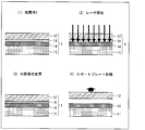
- the laminated body which concerns on this embodiment is demonstrated. If the laminated body of this embodiment is used as a laminated body which temporarily fixed the to-be-supported substrate to the support body, a specific use will not be specifically limited. In the following description, a stacked body in which a semiconductor wafer (supported substrate) is temporarily fixed to a support plate (support) used in a wafer support system will be described as an example. As shown in FIG. 1 (1), the laminate 1 according to this embodiment includes a substrate 11, a support plate (support) 12, an adhesive layer 14, and a separation layer 16.
- the substrate 11 is subjected to processes such as thinning and mounting while being supported by the support plate 12.
- the substrate 11 is not limited to a wafer substrate, and an arbitrary substrate such as a thin film substrate or a flexible substrate can be used. Further, a fine structure of an electronic element such as an electric circuit may be formed on the surface of the substrate 11 on the adhesive layer 14 side.
- the support plate 12 is a support body that supports the substrate 11 and has optical transparency. Therefore, when light is irradiated toward the support plate 12 from outside the stacked body 1, the light passes through the support plate 12 and reaches the separation layer 16. Further, the support plate 12 does not necessarily need to transmit all the light, and it is sufficient if the support plate 12 can transmit the light to be absorbed by the separation layer 16 (having a predetermined wavelength).
- the separation layer 16 is a layer formed of a material that changes in quality by absorbing light irradiated through the support.
- the “deterioration” of the separation layer 16 means a phenomenon that causes the separation layer 16 to be broken by receiving a slight external force or a state in which the adhesive force with the layer in contact with the separation layer 16 is reduced. Means.
- the separation layer 16 loses its strength or adhesiveness before being irradiated with light. Therefore, by applying a slight external force (for example, lifting the support plate 12), the separation layer 16 is broken, and the support plate 12 and the substrate 11 can be easily separated.
- the alteration of the separation layer 16 includes decomposition (exothermic or non-exothermic), cross-linking, configuration change or dissociation of functional groups due to absorbed light energy (and curing of the separation layer and degassing associated therewith). , Contraction or expansion) and the like.
- the alteration of the separation layer 16 occurs as a result of light absorption by the material constituting the separation layer 16. Therefore, the type of alteration of the separation layer 16 can be changed according to the type of material constituting the separation layer 16.
- the separation layer 16 is provided on the surface of the support plate 12 on the side where the substrate 11 is bonded via the adhesive layer 14. That is, the separation layer 16 is provided between the support plate 12 and the adhesive layer 14.
- the thickness of the separation layer 16 is, for example, 0.05 to 100 ⁇ m, more preferably 0.1 to 50 ⁇ m, still more preferably 0.1 to 10 ⁇ m, and particularly preferably 0.3 to 1 ⁇ m. If the thickness of the separation layer 16 is within the range of 0.05 to 100 ⁇ m, the separation layer 16 can be altered as desired by irradiation with light for a short time and irradiation with low energy light. The thickness of the separation layer 16 is particularly preferably within a range of 1 ⁇ m or less from the viewpoint of productivity.
- another layer may be further formed between the separation layer 16 and the support plate 12.
- the other layer should just be comprised from the material which permeate
- the wavelength of light that can be used differs depending on the type of material constituting the separation layer 16. Therefore, the material constituting the other layer does not need to transmit all light, and can be appropriately selected from materials capable of transmitting light having a wavelength that can alter the material constituting the separation layer 16.
- the separation layer 16 is preferably formed only from a material having a structure that absorbs light, but the material does not have a structure that absorbs light as long as the essential characteristics of the present invention are not impaired. May be added to form the separation layer 16. In addition, it is preferable that the surface of the separation layer 16 on the side facing the adhesive layer 14 is flat (unevenness is not formed), whereby the formation of the separation layer 16 can be easily performed, and Even in the pasting, it is possible to paste evenly.
- a material that forms the separation layer 16 as described below may be used by bonding it to the support plate 12 in advance, or the separation layer 16 may be formed on the support plate 12. You may use what applied the material and solidified in the film form.
- the method of applying the material constituting the separation layer 16 on the support plate 12 is appropriately selected from conventionally known methods such as chemical vapor deposition (CVD) deposition according to the type of material constituting the separation layer 16. it can.
- CVD chemical vapor deposition
- the separation layer 16 may be altered by absorbing light irradiated from the laser. That is, the light applied to the separation layer 16 to alter the separation layer 16 may be light emitted from a laser.
- lasers that emit light to irradiate the separation layer 16 include YAG lasers, ruby lasers, glass lasers, YVO 4 lasers, LD lasers, fiber lasers and other solid lasers, dye lasers and other liquid lasers, CO 2 lasers, Examples thereof include gas lasers such as excimer lasers, Ar lasers, and He—Ne lasers, laser beams such as semiconductor lasers and free electron lasers, and non-laser beams.
- the laser that emits light to irradiate the separation layer 16 can be appropriately selected according to the material constituting the separation layer 16, and irradiates light having a wavelength that can alter the material constituting the separation layer 16. Select the laser to be used.
- the separation layer 16 may contain a polymer containing a light-absorbing structure in its repeating unit.
- the polymer is altered by irradiation with light. The alteration of the polymer occurs when the structure absorbs the irradiated light.
- the separation layer 16 loses its strength or adhesiveness before being irradiated with light as a result of the alteration of the polymer. Therefore, by applying a slight external force (for example, lifting the support plate 12), the separation layer 16 is broken, and the support plate 12 and the substrate 11 can be easily separated.
- the above-mentioned structure having light absorptivity is a chemical structure in which a polymer containing the structure as a repeating unit is altered by light absorption by the structure.
- the structure is a chemical moiety containing a conjugated ⁇ -electron system consisting of, for example, a substituted or unsubstituted benzene ring, fused ring or heterocyclic ring. More specifically, the structure may be a cardo structure or a benzophenone structure, diphenyl sulfoxide structure, diphenyl sulfone structure (bisphenyl sulfone structure), diphenyl structure or diphenylamine structure present in the side chain of the polymer.
- the structure can be represented by the following formula:
- each R is independently an alkyl group, aryl group, halogen, hydroxyl group, ketone group, sulfoxide group, sulfone group, or N (R 1 ) (R 2 ) (where R 1 and R 2 are Each independently a hydrogen atom or an alkyl group having 1 to 5 carbon atoms), Z is absent or is CO—, —SO 2 —, —SO— or —NH—, and n is 0 or It is an integer from 1 to 5.
- the polymer includes, for example, a repeating unit represented by any one of (a) to (d) among the following formulas, represented by (e), or represented by (f) Contains structure in its main chain.
- l is an integer of 1 or more, m is 0 or an integer of 1 to 2, and X is any one of the formulas shown in the above “Chemical Formula 1” in (a) to (e). , (F) is any one of the formulas shown in the above “Chemical Formula 1” or does not exist, and Y 1 and Y 2 are each independently —CO— or SO 2 —. l is preferably an integer of 10 or less.
- Examples of the benzene ring, condensed ring and heterocyclic ring shown in the above “chemical formula 1” include phenyl, substituted phenyl, benzyl, substituted benzyl, naphthalene, substituted naphthalene, anthracene, substituted anthracene, anthraquinone, substituted anthraquinone, acridine, substituted Examples include acridine, azobenzene, substituted azobenzene, fluorin, substituted fluorin, fluorinone, substituted fluorin, carbazole, substituted carbazole, N-alkylcarbazole, dibenzofuran, substituted dibenzofuran, phenanthrene, substituted phenanthrene, pyrene and substituted pyrene.
- the substituent is, for example, alkyl, aryl, halogen atom, alkoxy, nitro, aldehyde, cyano, amide, dialkylamino, sulfonamide, imide, carboxylic acid, carboxylic acid Selected from esters, sulfonic acids, sulfonate esters, alkylaminos and arylaminos.
- the fifth substituent having two phenyl groups and Z is —C ( ⁇ O) — , 4-dihydroxybenzophenone, 2,3,4-trihydroxybenzophenone, 2,2 ', 4,4'-tetrahydroxybenzophenone, 2,2', 5,6'-tetrahydroxybenzophenone, 2-hydroxy-4- Methoxybenzophenone, 2-hydroxy-4-octoxybenzophenone, 2-hydroxy-4-dodecyloxybenzophenone, 2,2'-dihydroxy-4-methoxybenzophenone, 2,6-dihydroxy-4-methoxybenzophenone, 2,2 ' -Dihydroxy-4,4'-dimethoxybenzophenone, 4-amino-2'-hydroxybenzophenone, 4-di Tylamino-2'-hydroxybenzophenone, 4-diethylamino-2'-hydroxybenzophenone, 4-dimethylamino-4'-methoxy-2'-hydroxy
- the above structure can absorb light having a wavelength in a desired range by selecting the type.
- the wavelength of light that can be absorbed by the above structure is more preferably 100 to 2000 nm. Within this range, the wavelength of light that can be absorbed by the structure is on the shorter wavelength side, for example, 100 to 500 nm.
- the structure can alter the polymer containing the structure by absorbing ultraviolet light, preferably having a wavelength of about 300-370 nm.
- Light that can be absorbed by the above structure is, for example, a high-pressure mercury lamp (wavelength: 254 nm to 436 nm), a KrF excimer laser (wavelength: 248 nm), an ArF excimer laser (wavelength: 193 nm), an F2 excimer laser (wavelength: 157 nm), or XeCl.
- the separation layer 16 described above contains a polymer including the above structure as a repeating unit, but the separation layer 16 may further include a component other than the polymer.
- the component include a filler, a plasticizer, and a component that can improve the peelability of the support plate 12. These components are appropriately selected from conventionally known substances or materials that do not hinder or promote the absorption of light by the above structure and the alteration of the polymer.
- the separation layer 16 can be made of an inorganic material.
- the said inorganic substance is a material which changes in quality by light absorption.
- the separation layer 16 composed of such an inorganic material is altered by absorption of light, and loses strength or adhesiveness before being irradiated with light. Since the separation layer 16 that has been irradiated with light is broken by receiving a slight external force (for example, lifting the support plate 12), the support plate 12 and the substrate 11 can be easily separated.
- the said inorganic substance should just be a material which changes in quality by absorbing light, and the said inorganic substance can use suitably one or more types of inorganic substances selected from the group which consists of a metal, a metal compound, and carbon, for example.
- the metal compound refers to a compound containing a metal atom, and can be, for example, a metal oxide or a metal nitride.
- examples of such inorganic materials include, but are not limited to, gold, silver, copper, iron, nickel, aluminum, titanium, chromium, SiO 2 , SiN, Si 3 N 4 , TiN, and carbon.
- One or more inorganic substances selected from the group consisting of: Carbon is a concept that may include allotropes of carbon, and may be, for example, diamond, fullerene, diamond-like carbon, carbon nanotube, and the like.
- the above inorganic substance absorbs light having a wavelength in a specific range depending on the type.
- the inorganic material can be suitably altered.
- YAG laser YAG laser
- ruby laser glass laser
- YVO 4 laser LD laser
- fiber laser or other solid laser dye laser
- a liquid laser such as CO 2 laser, excimer laser, Ar laser, He—Ne laser or other gas laser, semiconductor laser, free electron laser or other laser light, or non-laser light may be used as appropriate.
- the separation layer 16 made of an inorganic material can be formed on the support plate 12 by a known technique such as sputtering, chemical vapor deposition (CVD), plating, plasma CVD, or spin coating.
- the thickness of the separation layer 16 made of an inorganic material is not particularly limited as long as it is a film thickness that can sufficiently absorb the light to be used. For example, a film thickness of 0.05 to 10 ⁇ m is more preferable.
- an adhesive may be applied in advance to both surfaces or one surface of an inorganic film (for example, a metal film) made of an inorganic material constituting the separation layer 16 and attached to the support plate 12 and the substrate 11.
- the separation layer 16 may be formed of a compound having an infrared absorbing structure.
- the compound is altered by absorbing infrared rays.
- the separation layer 16 loses its strength or adhesiveness before being irradiated with infrared rays as a result of the alteration of the compound. Therefore, by applying a slight external force (for example, lifting the support plate), the separation layer 16 is broken and the support plate 12 and the substrate 11 can be easily separated.
- Examples of the compound having an infrared absorptive structure or an infrared absorptive structure include alkanes, alkenes (vinyl, trans, cis, vinylidene, trisubstituted, tetrasubstituted, conjugated, cumulene, ring Formula), alkyne (monosubstituted, disubstituted), monocyclic aromatic (benzene, monosubstituted, disubstituted, trisubstituted), alcohol and phenols (free OH, intramolecular hydrogen bond, intermolecular hydrogen bond, saturated Secondary, saturated tertiary, unsaturated secondary, unsaturated tertiary), acetal, ketal, aliphatic ether, aromatic ether, vinyl ether, oxirane ether, peroxide ether, ketone, dialkylcarbonyl, aromatic Carbonyl, 1,3-diketone enol, o-hydroxy aryl ketone
- Examples of the structure containing the carbon-halogen bond include —CH 2 Cl, —CH 2 Br, —CH 2 I, —CF 2 —, —CF 3 , —CH ⁇ CF 2 , —CF ⁇ CF 2 , fluorine Aryl chloride, and aryl chloride.
- Examples of the structure including the Si—A 1 bond include SiH, SiH 2 , SiH 3 , Si—CH 3 , Si—CH 2 —, Si—C 6 H 5 , SiO aliphatic, Si—OCH 3 , Si—OCH. 2 CH 3 , Si—OC 6 H 5 , Si—O—Si, Si—OH, SiF, SiF 2 , SiF 3 and the like.
- As a structure including a Si—A 1 bond it is particularly preferable to form a siloxane skeleton and a silsesquioxane skeleton.
- the above structure can absorb infrared rays having a wavelength in a desired range by selecting the type.
- the wavelength of infrared rays that can be absorbed by the above structure is, for example, in the range of 1 ⁇ m to 20 ⁇ m, and the range of 2 ⁇ m to 15 ⁇ m can be more suitably absorbed.
- the structure is a Si—O bond, a Si—C bond, or a Ti—O bond, it can be in the range of 9 ⁇ m to 11 ⁇ m.
- the infrared wavelength that can be absorbed by each structure can be easily understood by those skilled in the art.
- non-patent literature SILVERSTEIN / BASSLER / MORRILL, “Identification method by spectrum of organic compound (5th edition) —Combination of MS, IR, NMR and UV” (published in 1992) The description on pages 146 to 151 may be referred to.
- a compound having an infrared absorbing structure used for forming the separation layer 16 among the compounds having the structure as described above, it can be dissolved in a solvent for coating and solidified to form a solid layer. As long as it is possible, there is no particular limitation.
- a resin that is a copolymer of a repeating unit represented by the following formula (1) and a repeating unit represented by the following formula (2), or A resin that is a copolymer of a repeating unit represented by the formula (1) and a repeating unit derived from an acrylic compound can be used.
- R 1 is hydrogen, an alkyl group having 10 or less carbon atoms, or an alkoxy group having 10 or less carbon atoms
- a tert-butylstyrene (TBST) -dimethylsiloxane copolymer which is a copolymer of a repeating unit represented by the above formula (1) and a repeating unit represented by the following formula (3) is used.
- a polymer is more preferable, and a TBST-dimethylsiloxane copolymer containing a repeating unit represented by the above formula (1) and a repeating unit represented by the following formula (3) in a ratio of 1: 1 is further preferable.
- a resin that is a copolymer of a repeating unit represented by the following formula (4) and a repeating unit represented by the following formula (5) can be used.
- R 2 is hydrogen or an alkyl group having 1 to 10 carbon atoms
- R 3 is an alkyl group having 1 to 10 carbon atoms, or a phenyl group.
- the copolymer contains a repeating unit represented by the following formula (7) in a ratio of 7: 3.
- the polymer having a silsesquioxane skeleton may have a random structure, a ladder structure, and a cage structure, and any structure may be used.
- Examples of the compound containing a Ti—O bond include (i) tetra-i-propoxytitanium, tetra-n-butoxytitanium, tetrakis (2-ethylhexyloxy) titanium, and titanium-i-propoxyoctylene glycolate.
- chelating titanium such as (ii) di-i-propoxy bis (acetylacetonato) titanium and propanedioxytitanium bis (ethylacetoacetate), (iii) iC 3 H 7 O — [— Ti (Oi-C 3 H 7 ) 2 —O—] n—iC 3 H 7 and nC 4 H 9 O— [Ti (On—C 4 H 9 ) 2 —O— ] N- n-C 4 H 9 and other titanium polymers, (iv) tri-n-butoxytitanium monostearate, titanium stearate, di-i-propoxytitanium diiso Stearate, and acylate titanium such as (2-n-butoxycarbonylbenzoyloxy) tributoxytitanium, and (v) water-soluble titanium compounds such as di-n-butoxy-bis (triethanolaminato) titanium. .
- di-n-butoxy bis (triethanolaminato) titanium Ti (OC 4 H 9 ) 2 [OC 2 H 4 N (C 2 H 4 OH) 2 ] 2 ) is preferred.
- the separation layer 16 described above contains a compound having an infrared absorbing structure
- the separation layer 16 may further include a component other than the above compound.
- the component include a filler, a plasticizer, and a component that can improve the peelability of the support plate 12. These components are appropriately selected from conventionally known substances or materials that do not interfere with or promote infrared absorption by the above structure and alteration of the compound.
- the separation layer 16 can be composed of a fluorocarbon. Fluorocarbon is altered by the absorption of light.
- the separation layer 16 made of fluorocarbon is altered by absorption of light, and loses strength or adhesiveness before being irradiated with light. Since the separation layer 16 that has been irradiated with light is broken by receiving a slight external force (for example, lifting the support plate 12), the support plate 12 and the substrate 11 can be easily separated.
- the fluorocarbon constituting the separation layer 16 can be suitably formed by a plasma CVD method.
- fluorocarbon includes CxFy (perfluorocarbon) and CxHyFz (x, y, and z are positive integers), but is not limited thereto, for example, CHF 3 , CH 2 F 2 , C 2 H 2 F 2 , C 4 F 8 , C 2 F 6 , C 5 F 8, etc.
- an inert gas such as nitrogen, helium, or argon, a hydrocarbon such as oxygen, alkane, or alkene, and carbon dioxide or hydrogen are added to the fluorocarbon used to configure the separation layer 16 as necessary. May be. Further, a mixture of these gases may be used (a mixed gas of fluorocarbon, hydrogen, nitrogen, etc.).
- the separation layer 16 may be composed of a single type of fluorocarbon, or may be composed of two or more types of fluorocarbon.
- Fluorocarbon absorbs light having a wavelength in a specific range depending on its type. By irradiating the separation layer with light having a wavelength within a range that is absorbed by the fluorocarbon used in the separation layer 16, the fluorocarbon can be suitably altered.
- the light applied to the separation layer 16 is a liquid such as a solid laser such as a YAG laser, a ruby laser, a glass laser, a YVO 4 laser, an LD laser, or a fiber laser, or a dye laser depending on the wavelength that can be absorbed by the fluorocarbon.
- a gas laser such as a laser, a CO 2 laser, an excimer laser, an Ar laser, or a He—Ne laser, a laser beam such as a semiconductor laser or a free electron laser, or a non-laser beam may be used as appropriate.
- the wavelength at which the fluorocarbon can be altered is not limited to this, but for example, a wavelength in the range of 600 nm or less can be used.
- the separation layer 16 may contain an infrared absorbing material.
- An infrared absorbing material is a material that is altered by the absorption of light.
- the separation layer 16 configured to contain an infrared absorbing material is altered by absorption of light and loses strength or adhesiveness before being irradiated with light. Since the separation layer 16 that has been irradiated with light is broken by receiving a slight external force (for example, lifting the support plate 12), the support plate 12 and the substrate 11 can be easily separated.
- the infrared absorbing material may be any material that is altered by absorbing infrared rays, and for example, carbon black, iron particles, or aluminum particles can be suitably used as the infrared absorbing material.
- the infrared absorbing material absorbs light having a wavelength in a specific range depending on the type. By irradiating the separation layer 16 with light having a wavelength in a range that is absorbed by the infrared absorbing material used for the separation layer 16, the infrared absorbing material can be suitably altered.
- the separation layer 16 can be a layer formed by plasma treatment using a reactive gas.
- the reaction gas preferably contains an organic compound having an unsaturated bond and a fluorine compound.
- the organic compound is not particularly limited as long as it has an unsaturated bond, and examples thereof include alkenes, cycloalkenes, alkynes, and aromatic compounds.
- alkene examples include 1,2-butadiene, 1,3-butadiene, 2,3-dimethyl-1,3-butadiene, 3-methyl-1,2-butadiene, isoprene, and the like.
- cycloalkene examples include 1,3-hexadiene, 1,4-hexadiene, cyclopentadiene, 1,5-cyclooctadiene, and the like.
- alkyne acetylene etc. can be mentioned, for example.
- the aromatic compound examples include benzene, toluene, xylene, styrene and the like.
- an organic compound having an ether bond, an ester bond, a siloxy bond, or the like can be used.
- the organic compound having an ether bond and / or a siloxy bond examples include 1-methoxy-3- (trimethylsilyloxy) -1,3-butadiene and 2-trimethylsilyloxy-1,3-butadiene.
- Examples of the organic compound having an ester bond examples include ethyl 2,3-butadiene acid.
- the organic compound is preferably an alkene or a cycloalkene.
- Alkenes or cycloalkenes have a structure that is not easily destroyed by low-density plasma. For this reason, by containing alkene or cycloalkene in the reaction gas, the alkene or cycloalkene can be suitably polymerized in the plasma treatment without excessive destruction. Also, unsaturated bonds can be introduced into the separation layer 16 formed by plasma treatment. Therefore, by using alkene or cycloalkene as the organic compound, it is possible to suitably form the separation layer 16 that is altered by absorbing light.
- the organic compound preferably has two or more unsaturated bonds.
- the separation layer 16 that can absorb light more preferably can be formed.
- the organic compound preferably has a boiling point in the range of 30 ° C. or more and 100 ° C. or less, more preferably in the range of 30 ° C. or more and 60 ° C. or less, and in the range of 40 ° C. or more and 50 ° C. or less. Most preferably. If the boiling point of the organic compound is in the range of 30 ° C. or higher and 100 ° C. or lower, the organic compound can be suitably used as the reaction gas under the conditions for the plasma treatment.
- Examples of the fluorine compound contained in the reaction gas used in the method for manufacturing a laminate according to this embodiment include fluorocarbon, carbon tetrafluoride (CF 4 ), nitrogen trifluoride (NF 3 ), and sulfur hexafluoride (SF). 6 ) and the like.
- Examples of the fluorocarbon include C 4 F 8 and the like.
- the plasma processing apparatus used for the plasma processing is not particularly limited, and a known plasma processing apparatus can be used.
- the electrode provided in the plasma processing apparatus is not particularly limited, and may be, for example, a dual coil antenna, a single coil antenna, or a parallel plate electrode, but a separation layer formed on a support by using a parallel plate electrode.
- the surface area of 16 can be increased, and as a result, a laminate can be manufactured using a substrate having a larger diameter.
- the shape of the reaction chamber of the plasma processing apparatus is not particularly limited, and may be a dome shape or other shapes such as a cylindrical shape.
- the size of the reaction chamber may be appropriately selected according to the size of the substrate to be processed.
- the material of the reaction chamber can be appropriately selected from known materials that do not hinder the plasma treatment and the formation of the separation layer 16.
- the plasma generated in the plasma processing apparatus includes capacitively coupled plasma (CCP: Conductive Coupled Plasma) by an electrostatic field generated by a high frequency power applied to a coil electrode or a parallel plate electrode, and inductive coupling by an induction electric field generated by a high frequency current flowing through the coil electrode.
- CCP Conductive Coupled Plasma
- ICP Inductive Coupled Plasma
- the plasma treatment in the separation layer forming step is preferably a low density plasma treatment.
- the low density plasma is a plasma having an ion density of 1 ⁇ 10 10 cm ⁇ 3 or less, and means a plasma mainly composed of capacitive coupling.
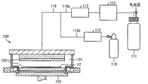
- FIG. 2 is a schematic diagram illustrating a separation layer manufacturing process included in the manufacturing method according to an embodiment of the present invention.
- the plasma processing apparatus 100 used in the separation layer forming process included in the laminate manufacturing method according to the present embodiment has a pair of parallel plate electrodes 102 and a support plate 12 placed in a reaction chamber 101. Stage 103 is provided.
- the plasma processing apparatus 100 communicates with the container 111 storing the organic compound so as to pass through the liquid mass flow controller 112 and the vaporizer 113 through the pipe 116a, and passes through the mass flow controller 115 through the pipe 116b.
- the fluorine compound cylinder 114 communicates. Further, the pipes 116 a and 116 b merge with the pipe 116.
- the reaction chamber 101 is used for forming the separation layer 16 from the reaction gas by plasma treatment. Moreover, the reaction chamber 101 can adjust the pressure in the reaction chamber 101 by a vacuum pump (not shown).
- the pair of parallel plate electrodes 102 are provided in the reaction chamber 101 and generate plasma using a reaction gas by applying high-frequency power.
- the stage 103 includes one of the pair of parallel plate electrodes 102 so that the support plate 12 can be placed thereon.
- the container 111 stores an organic compound used for the reaction gas, and supplies the organic compound to the liquid mass flow controller 112 via the pipe 116a by pressurizing with nitrogen.
- the liquid mass flow controller 112 is a device that adjusts the flow rate of the organic compound, and adjusts the flow rate of the organic compound supplied to the vaporizer 113 via the pipe 116a.
- the fluorine compound cylinder 114 is a cylinder storing a fluorine compound used as a reaction gas, and supplies the fluorine gas to the mass flow controller 115 through the pipe 116b.
- the mass flow controller 115 is a device that adjusts the flow rate of the fluorine gas, and adjusts the flow rate of the fluorine gas supplied through the pipe 116b.
- the piping 116 can be prevented from being liquefied by being heated.
- the support plate 12 is placed on the stage 103 provided with one of the pair of parallel plate electrodes 102 in the reaction chamber 101.
- a preheating step of preheating the inside of the reaction chamber 101 and the support plate 12 may be performed.
- the surface of the support plate 12 may be cleaned by adding oxygen gas to the pretreatment gas.
- a reaction gas that becomes the separation layer 16 is supplied into the reaction chamber 101, and the separation layer 16 is formed on the support plate 12 by plasma treatment.
- the organic compound contained in the reaction gas is supplied from the container 111, the flow rate is adjusted by the liquid mass flow controller 112, and the vaporizer 113 vaporizes the organic compound.
- the fluorine compound is supplied from the fluorine compound cylinder 114 and the flow rate is adjusted by the mass flow controller 115. Thereafter, the vaporized organic compound and fluorine compound are mixed in the pipe 116 and supplied into the reaction chamber 101 while being heated.
- the volume ratio of the organic compound and the fluorine compound contained in the reaction gas can be adjusted by adjusting the flow rates of the organic compound and the fluorine gas with the liquid mass flow controller 112 and the mass flow controller 115.
- the volume ratio of the organic compound to the fluorine compound is 6: 4 to 9: 1
- the separation layer 16 having no chemical resistance and good brittleness can be formed.
- the separation layer 16 that can be suitably removed by the cleaning liquid can be formed.
- the volume ratio of the organic compound and the fluorine compound can be adjusted during the separation layer forming step.
- inert gases such as nitrogen, helium and argon, and additional gases such as hydrogen and oxygen may be added to the reaction gas.
- the target temperature in the reaction chamber 101 is not particularly limited, and a known temperature can be used, but it is more preferably in the range of 100 ° C. or higher and 300 ° C. or lower, and the range of 200 ° C. or higher and 250 ° C. or lower. It is particularly preferred that By setting the temperature in the reaction chamber to such a range, the plasma treatment can be suitably performed.
- the thickness of the separation layer 16 formed in the separation layer forming step is not particularly limited as long as it is a film thickness that can sufficiently absorb the light to be used.
- the range is 0.5 ⁇ m or more and 2.0 ⁇ m or less.
- the film thickness is more preferably within the range of 1.0 ⁇ m or more and 1.5 or less. What is necessary is just to set the formation time of the separation layer 16 in a separation layer formation process according to the film thickness to form.
- the separation layer 16 can include a first separation layer 16 a and a second separation layer 16 b.
- the laminate 20 has the same configuration as that of the laminate 1 except that the separation layer 16 has two layers.
- the first separation layer 16a is formed by the plasma processing apparatus 100 of FIG. 2 using a reactive gas containing an organic compound having an unsaturated bond and a fluorine compound.
- the second separation layer 16b is a layer that does not correspond to the first separation layer 16a and is formed of a material that is altered by the light irradiation exemplified in this specification.
- the first separation layer 16a and the second separation layer 16b are formed on the support.
- the first separation layer 16a has chemical resistance in various chemical treatments
- the second separation layer 16b has good separation properties after irradiation with light.
- the first separation layer 16a can prevent the second separation layer 16b from being altered by chemical treatment.
- the second separation layer 16b is on the first separation layer 16a
- the first separation layer 16a functions as a separation layer even if the second separation layer 16b is altered by chemical treatment. It can be secured.
- the separation layer can be suitably altered and the substrate can be easily separated from the laminate.
- optical density In general, the optical density (hereinafter referred to as OD value) is obtained by the following equation (1).
- D ⁇ log (I / I 0 ) (1)
- D is the OD value
- I is the intensity of incident light
- I 0 is the intensity of transmitted light.
- the OD value of the separation layer 16 is evaluated based on the OD value measured using an X-Rite 310 (OD value measuring machine: manufactured by X-Rite).
- the OD value of the separation layer 16 of the laminate 1 is preferably 0.20 or more and 1.00 or less, and more preferably 0.30 or more and 1.00 or less. In the range where the OD value of the separation layer 16 is 0.20 or more and 1.00 or less (particularly, the range of 0.30 or more and 1.00 or less, and so on), the laser beam is applied so that the substrate 11 is not damaged. The present inventors have found that irradiation time can be reduced and the film formation time of the separation layer 16 can be shortened.
- damage to the substrate 11 can be suitably prevented under the following conditions.
- the OD value of the separation layer 16 is set to 0.20 or more and 1.00 or less, it is preferable to set the irradiation condition of the laser light as follows.
- the average output value of the laser beam is preferably in the range of 1.0 W or more and 5.0 W or less, and more preferably in the range of 3.0 W or more and 4.0 W or less.
- the repetition frequency of the laser light is preferably in the range of 20 kHz or more and 60 kHz or less, and more preferably in the range of 30 kHz or more and 50 kHz or less.
- the wavelength of the laser light is preferably 300 nm or more and 700 nm or less, and more preferably 450 nm or more and 650 nm or less. According to such conditions, the energy of the pulsed light applied to the separation layer 16 can be set to an appropriate condition for altering the separation layer 16 while preventing damage to the substrate 11.
- the beam spot diameter of the pulsed light used in the separation step of the separation layer 16 is preferably 100 ⁇ m or more and 250 ⁇ m or less, and more preferably 120 ⁇ m or more and 230 ⁇ m or less.
- the irradiation pitch of the pulsed light may be any pitch that does not overlap adjacent beam spots and can change the separation layer 16, but is preferably 110 ⁇ m or more and 250 ⁇ m or less, preferably 160 ⁇ m or more, More preferably, it is 220 ⁇ m or less.
- the irradiation speed of the pulse light may be any speed that can change the separation layer 16, but is preferably 4000 mm / s or more and 10000 mm / s or less, preferably 5000 mm / s or more and 8000 mm / s or less. It is more preferable that
- the pulse width of the pulsed light applied to the separation layer 16 is preferably 20 nanoseconds or more. More preferably, it is 40 nanoseconds or more, More preferably, it is 70 nanoseconds or more.
- the upper limit of the pulse width of the pulsed light applied to the separation layer 16 is preferably 200 nanoseconds, and more preferably 150 nanoseconds.
- the OD value of the separation layer 16 varies depending on the type of material constituting the separation layer 16. Further, for example, when the separation layer 16 is formed by a chemical vapor deposition (CVD) method, the thickness varies depending on the density of the material constituting the separation layer 16. In this case, the density of the separation layer 16 can be adjusted by changing the film formation time of the separation layer 16 by chemical vapor deposition (CVD), the injection rate of the source gas, and the like.
- CVD chemical vapor deposition
- the separation layer 16 is preferably formed only from a material having a structure that absorbs light, but the material does not have a structure that absorbs light as long as the essential characteristics of the present invention are not impaired. Can also be added to adjust the OD value.
- the adhesive layer 14 is configured to adhere and fix the substrate 11 to the support plate 12 and at the same time to cover and protect the surface of the substrate 11. Therefore, the adhesive layer needs to have adhesiveness and strength for maintaining the fixing of the substrate 11 to the support plate 12 and the covering of the surface to be protected of the substrate 11 when the substrate 11 is processed or transported. . On the other hand, when it becomes unnecessary to fix the substrate 11 to the support plate 12, it needs to be easily peeled or removed from the substrate 11.
- the adhesive layer 14 usually has strong adhesiveness, and the adhesive layer 14 is composed of an adhesive whose adhesiveness is reduced by some treatment or has solubility in a specific solvent.
- the thickness of the adhesive layer 14 is more preferably 1 to 200 ⁇ m, and further preferably 10 to 150 ⁇ m.
- the adhesive layer 14 can be formed by applying an adhesive material as described below onto the substrate 11 by a conventionally known method such as spin coating.
- adhesive for example, various adhesives known in the art such as acrylic, novolak, naphthoxan, hydrocarbon, polyimide, and elastomer are adhesives that constitute the adhesive layer 14 according to the present embodiment. It can be used. Below, the composition of resin which the contact bonding layer 14 in this embodiment contains is demonstrated.
- the resin contained in the adhesive layer 14 may be any resin as long as it has adhesiveness, for example, a hydrocarbon resin, an acrylic-styrene resin, a maleimide resin, an elastomer resin, or a combination thereof.
- the hydrocarbon resin is a resin that has a hydrocarbon skeleton and is obtained by polymerizing a monomer composition.
- cycloolefin polymer hereinafter sometimes referred to as “resin (A)”
- resin (A) cycloolefin polymer
- resin (B) at least one resin selected from the group consisting of terpene resin, rosin resin and petroleum resin
- Resin (A) may be a resin obtained by polymerizing a monomer component containing a cycloolefin monomer.
- Specific examples of the resin (A) include a ring-opening (co) polymer of a monomer component containing a cycloolefin monomer, and a resin obtained by addition (co) polymerization of a monomer component containing a cycloolefin monomer. Can be mentioned.
- Examples of the cycloolefin monomer contained in the monomer component constituting the resin (A) include bicyclic compounds such as norbornene and norbornadiene, tricyclic compounds such as dicyclopentadiene and dihydroxypentadiene, and tetracyclododecene.
- Tetracycles pentacycles such as cyclopentadiene trimer, heptacycles such as tetracyclopentadiene, or polycyclic alkyl (methyl, ethyl, propyl, butyl, etc.) substituted alkenyls (vinyl, etc.) Examples include substituted, alkylidene (such as ethylidene) substituted, aryl (such as phenyl, tolyl, naphthyl) substituted, and the like.
- norbornene-based monomers selected from the group consisting of norbornene, tetracyclododecene, and alkyl-substituted products thereof are particularly preferable.
- the monomer component constituting the resin (A) may contain another monomer copolymerizable with the above-described cycloolefin monomer, and preferably contains, for example, an alkene monomer.
- alkene monomer examples include ethylene, propylene, 1-butene, isobutene, 1-hexene, ⁇ -olefin, and the like.
- the alkene monomer may be linear or branched.
- a cycloolefin monomer is contained as a monomer component constituting the resin (A) from the viewpoint of high heat resistance (low thermal decomposability, low thermal weight reduction).
- the ratio of the cycloolefin monomer to the whole monomer component constituting the resin (A) is preferably 5 mol% or more, more preferably 10 mol% or more, and further preferably 20 mol% or more. preferable.
- the ratio of the cycloolefin monomer to the whole monomer component constituting the resin (A) is not particularly limited, but is preferably 80 mol% or less from the viewpoint of solubility and stability over time in a solution, More preferably, it is 70 mol% or less.
- a linear or branched alkene monomer may be contained as a monomer component constituting the resin (A).
- the ratio of the alkene monomer to the whole monomer component constituting the resin (A) is preferably 10 to 90 mol%, more preferably 20 to 85 mol% from the viewpoint of solubility and flexibility. 30 to 80 mol% is more preferable.
- the resin (A) is a resin having no polar group, such as a resin obtained by polymerizing a monomer component composed of a cycloolefin monomer and an alkene monomer, at high temperatures. It is preferable for suppressing generation of gas.
- the polymerization method and polymerization conditions for polymerizing the monomer component are not particularly limited and may be appropriately set according to a conventional method.
- Examples of commercially available products that can be used as the resin (A) include “TOPAS” manufactured by Polyplastics Co., Ltd., “APEL” manufactured by Mitsui Chemicals, Inc., “ZEONOR” and “ZEONEX” manufactured by Zeon Corporation. And “ARTON” manufactured by JSR Corporation.
- the glass transition point (Tg) of the resin (A) is preferably 60 ° C. or higher, and particularly preferably 70 ° C. or higher.
- Tg glass transition point
- Resin (B) is at least one resin selected from the group consisting of terpene resins, rosin resins and petroleum resins.
- terpene resin examples include terpene resins, terpene phenol resins, modified terpene resins, hydrogenated terpene resins, hydrogenated terpene phenol resins, and the like.
- rosin resin examples include rosin, rosin ester, hydrogenated rosin, hydrogenated rosin ester, polymerized rosin, polymerized rosin ester, and modified rosin.
- Examples of petroleum resins include aliphatic or aromatic petroleum resins, hydrogenated petroleum resins, modified petroleum resins, alicyclic petroleum resins, coumarone-indene petroleum resins, and the like. Among these, hydrogenated terpene resins and hydrogenated petroleum resins are more preferable.
- the softening point of the resin (B) is not particularly limited, but is preferably 80 to 160 ° C.
- the softening point of the resin (B) is 80 ° C. or higher, the adhesive laminate can be suppressed from being softened when exposed to a high temperature environment, and adhesion failure does not occur.
- the softening point of the resin (B) is 160 ° C. or less, the resin (B) exhibits a good peeling rate when peeling the adhesive laminate.
- the molecular weight of the resin (B) is not particularly limited, but is preferably 300 to 3000. When the molecular weight of the resin (B) is 300 or more, the resin (B) exhibits sufficient heat resistance and the degassing amount is reduced under a high temperature environment. On the other hand, when the molecular weight of the resin (B) is 3000 or less, the resin (B) exhibits a good peeling rate when peeling the adhesive laminate.
- the molecular weight of resin (B) in this embodiment means the molecular weight of polystyrene conversion measured by gel permeation chromatography (GPC).
- the mixture may use what mixed resin (A) and resin (B) as resin.
- the mixture exhibits good heat resistance and peel rate.
- the mixture has a peeling rate and a high temperature environment. It is preferable because of its excellent heat resistance and flexibility.
- acryl-styrene resin examples include a resin obtained by polymerization using styrene or a styrene derivative and (meth) acrylic acid ester as monomers.
- Examples of the (meth) acrylic acid ester include a (meth) acrylic acid alkyl ester having a chain structure, a (meth) acrylic acid ester having an aliphatic ring, and a (meth) acrylic acid ester having an aromatic ring.
- Examples of the (meth) acrylic acid alkyl ester having a chain structure include an acrylic long-chain alkyl ester having an alkyl group having 15 to 20 carbon atoms and an acrylic alkyl ester having an alkyl group having 1 to 14 carbon atoms. .
- acrylic long-chain alkyl ester examples include acrylic acid or methacrylic acid whose alkyl group is n-pentadecyl group, n-hexadecyl group, n-heptadecyl group, n-octadecyl group, n-nonadecyl group, n-eicosyl group, etc.
- alkyl esters examples include alkyl esters.
- the alkyl group may be branched.
- acrylic alkyl ester having an alkyl group having 1 to 14 carbon atoms examples include known acrylic alkyl esters used in existing acrylic adhesives.
- esters examples include esters.
- Examples of (meth) acrylic acid ester having an aliphatic ring include cyclohexyl (meth) acrylate, cyclopentyl (meth) acrylate, 1-adamantyl (meth) acrylate, norbornyl (meth) acrylate, isobornyl (meth) acrylate, and tricyclodecanyl.
- (Meth) acrylate, tetracyclododecanyl (meth) acrylate, dicyclopentanyl (meth) acrylate and the like can be mentioned, and isobornyl methacrylate and dicyclopentanyl (meth) acrylate are more preferable.
- the (meth) acrylic acid ester having an aromatic ring is not particularly limited.
- the aromatic ring include a phenyl group, a benzyl group, a tolyl group, a xylyl group, a biphenyl group, a naphthyl group, and an anthracenyl group.
- the aromatic ring may have a linear or branched alkyl group having 1 to 5 carbon atoms. Specifically, phenoxyethyl acrylate is preferable.
- maleimide resins include N-methylmaleimide, N-ethylmaleimide, Nn-propylmaleimide, N-isopropylmaleimide, Nn-butylmaleimide, N-isobutylmaleimide, N-sec as monomers.
- Males having an aliphatic hydrocarbon group such as maleimide having an alkyl group, N-cyclopropylmaleimide, N-cyclobutylmaleimide, N-cyclopentylmaleimide, N-cyclohexylmaleimide, N-cycloheptylmaleimide, N-cyclooctylmaleimide Resins obtained by polymerizing aromatic maleimides having an aryl group such as imide, N-phenylmaleimide, Nm-methylphenylmaleimide, No-methylphenylmaleimide, and Np-methylphenylmaleimide It is done.
- aryl group such as imide, N-phenylmaleimide, Nm-methylphenylmaleimide, No-methylphenylmaleimide, and Np-methylphenylmaleimide It is done.
- a cycloolefin copolymer that is a copolymer of a repeating unit represented by the following chemical formula (8) and a repeating unit represented by the following chemical formula (9) can be used as the resin of the adhesive component.
- n is 0 or an integer of 1 to 3.
- APL 8008T, APL 8009T, APL 6013T (all manufactured by Mitsui Chemicals, Inc.) and the like can be used.
- the adhesive layer 14 it is preferable to form the adhesive layer 14 using a resin other than a photocurable resin (for example, a UV curable resin).
- a resin other than a photocurable resin for example, a UV curable resin
- the photocurable resin may remain as a residue around the minute irregularities of the substrate 11 after the adhesive layer 14 is peeled or removed.
- an adhesive that dissolves in a specific solvent is preferable as a material constituting the adhesive layer 14. This is because the adhesive layer 14 can be removed by dissolving it in a solvent without applying a physical force to the substrate 11. When the adhesive layer 14 is removed, the adhesive layer 14 can be easily removed without damaging or deforming the substrate 11 even from the substrate 11 whose strength has decreased.
- hexane, heptane, octane, nonane, methyloctane, decane, undecane, dodecane, tridecane, and other linear hydrocarbons, having 3 to 15 carbon atoms are used.
- hydrocarbons eg), p-menthane, o-menthane, m-menthane, diphenylmenthane, 1,4-terpine, 1,8-terpin, bornane, norbornane, pinane, tujang, kalan, longifolene, geraniol , Nerol, linalool, citral, citronellol, menthol, isomenthol, neomenthol, ⁇ -terpineol, ⁇ -terpineol, ⁇ -terpineol, terpinen-1-ol, terpinen-4-ol, dihydroterpinyl acetate, 1,4 -Cineol, 1,8-Cineol Terpene solvents such as borneol, carvone, yonon, thuyon, camphor, d-limonene, l-limonene, dipentene; lactones such as ⁇ -butyrol
- the elastomer preferably contains a styrene unit as a constituent unit of the main chain.
- the elastomer used as the adhesive preferably has a styrene unit content in the range of 14% by weight to 50% by weight.
- the elastomer preferably has a weight average molecular weight in the range of 10,000 to 200,000.
- elastomers examples include polystyrene-poly (ethylene / propylene) block copolymer (SEP), styrene-isoprene-styrene block copolymer (SIS), styrene-butadiene-styrene block copolymer (SBS), and styrene-butadiene-butylene-styrene block.
- SEP polystyrene-poly (ethylene / propylene) block copolymer
- SIS styrene-isoprene-styrene block copolymer
- SBS styrene-butadiene-styrene block copolymer
- styrene-butadiene-butylene-styrene block examples include polystyrene-poly (ethylene / propylene) block copolymer (SEP), styrene-isoprene-s
- SBBS ethylene-propylene terpolymer
- EPT ethylene-propylene terpolymer
- SEBS styrene-ethylene-butylene-styrene block copolymer
- SEPS styrene-ethylene-propylene-styrene block copolymer
- SEEPS styrene-ethylene-ethylene-propylene-styrene block copolymer
- the adhesive material may further contain other miscible substances as long as the essential characteristics of the present invention are not impaired.
- various conventional additives such as additional resins, plasticizers, adhesion aids, stabilizers, colorants, antioxidants and surfactants for improving the performance of the adhesive may be further used. it can.
- the separation layer 16 is irradiated with pulsed laser light through the support plate 12 (irradiation process). . At this time, the irradiated laser light passes through the light-transmitting support plate 12 and reaches the separation layer 16.
- the separation layer 16 is altered as shown in (2) in FIG. 1 by absorbing the laser beam that has arrived. Thereby, the adhesion between the substrate 11 and the support plate 12 is weakened, and the support plate 12 is easily separated from the substrate 11 as shown in FIG.
- the separation layer 16 In order to separate the support plate 12 from the laminate 1, when the separation layer 16 is irradiated with laser light from the support plate 12 side, the laser light may leak from the separation layer 16.
- the leaked light reaches the substrate 11, and the substrate 11 itself or an electronic element such as an electronic circuit to be protected formed on the substrate 11 may be adversely affected by the leaked light.
- adverse effects of leaked light include disassembly of electronic circuits mounted on the substrate 11, damage to the substrate 11, and the like.
- an OD value of the separation layer 16 may be selected from 0.20 to 1.00. Such selection of the OD value in the separation layer 16 makes it possible to change the separation layer 16 in a desired manner without damaging the substrate 11 with the transmitted light of the laser light by irradiation with the laser beam.
- damage to the substrate 11 can be suitably prevented under the following conditions.
- the OD value of the separation layer 16 is set to 0.20 or more and 1.00 or less, it is preferable to set the irradiation condition of the laser light as follows.
- the average output value of the laser beam is preferably in the range of 1.0 W or more and 5.0 W or less, and more preferably in the range of 3.0 W or more and 4.0 W or less.
- the repetition frequency of the laser light is preferably in the range of 20 kHz or more and 60 kHz or less, and more preferably in the range of 30 kHz or more and 50 kHz or less.
- the wavelength of the laser light is preferably 300 nm or more and 700 nm or less, and more preferably 450 nm or more and 650 nm or less. According to such conditions, the energy of the pulsed light applied to the separation layer 16 can be set to an appropriate condition for altering the separation layer 16 while preventing damage to the substrate 11.
- the beam spot diameter of the pulsed light used in the separation step of the separation layer 16 is preferably 100 ⁇ m or more and 250 ⁇ m or less, and more preferably 120 ⁇ m or more and 230 ⁇ m or less.
- the irradiation pitch of the pulsed light may be any pitch that does not overlap adjacent beam spots and can change the separation layer 16, but is preferably 110 ⁇ m or more and 250 ⁇ m or less, preferably 160 ⁇ m or more, More preferably, it is 220 ⁇ m or less.
- the irradiation speed of the pulse light may be any speed that can change the separation layer 16, but is preferably 4000 mm / s or more and 10000 mm / s or less, preferably 5000 mm / s or more and 8000 mm / s or less. It is more preferable that
- the pulse width of the pulsed light applied to the separation layer 16 is preferably 20 nanoseconds or more. More preferably, it is 40 nanoseconds or more, More preferably, it is 70 nanoseconds or more.
- the upper limit of the pulse width of the pulsed light applied to the separation layer 16 is preferably 200 nanoseconds, and more preferably 150 nanoseconds.
- the irradiation apparatus for irradiating pulsed light in the method for separating the laminate is not particularly limited as long as the separation layer 16 can be irradiated with pulsed light having a pulse width of 20 nanoseconds or more.
- An oscillator appropriately selected from laser oscillators and the like can be used.
- the irradiation device can be selected as appropriate according to the material constituting the separation layer 16, and a laser that irradiates light capable of altering the material constituting the separation layer 16 may be selected.
- the frequency of the laser beam is preferably 300 nm to 700 nm. When the frequency of the laser light is within the range, it becomes easy to alter the separation layer 16 without damaging the substrate 11 and the electronic device formed on the substrate 11 with the laser light applied to the separation layer.
- the irradiation step it is preferable to uniformly irradiate the entire laminate 1 with pulsed light.
- the separation layer 16 can be altered so that the substrate 11 and the support plate 12 can be easily separated, the laminate can be used. 1 may be partially irradiated with pulsed light.
- the separation method of the laminate by adjusting the OD value of the separation layer 16 to 0.20 or more and 1.00 or less, an appropriate repetition frequency and average output of the pulsed laser light can be set. is there. Therefore, since the laser light set appropriately is irradiated, even if the light leaked without being absorbed in the separation layer 16 reaches the substrate 11, it may damage the substrate 11 and the electronic elements formed on the substrate 11. Absent. In addition, since the separation layer 16 can be irradiated with light having an energy intensity necessary for altering the separation layer 16, the substrate 11 and the support plate 12 can be easily separated.
- the substrate 11 and the support plate 12 can be easily separated by light irradiation after the manufacturing process while realizing strong adhesion between the substrate 11 and the support plate 12 during the manufacturing process. In addition to being possible, there is an effect that the adverse effect on the substrate 11 by light can be prevented.
- the present invention provides a method for evaluating a separation layer including a measurement step of measuring the OD value of the separation layer. That is, as described above, if the OD value of the separation layer is within a predetermined range, damage to the substrate surface can be prevented. Therefore, by measuring the OD value of the separation layer, it can be evaluated whether or not the separation layer does not transmit light that damages the substrate surface.
- the separation layer evaluation method when the OD value of the separation layer measured in the measurement step is 0.20 or more, it is determined that the separation layer does not transmit light that damages the substrate surface. it can. More preferably, when the OD value of the separation layer measured in the measurement step is 0.20 or more and 1.00 or less, it can be determined that the separation layer does not transmit light that causes damage to the substrate surface. In this way, it is possible to avoid the manufacture of defective products due to damage received on the substrate surface in the irradiation step. In addition, it is preferable that the average output value of the laser beam in the irradiation process at this time is 1.0 W or more and 5.0 W or less, and more preferably 3.0 W or more and 4.0 W or less. .
- the repetition frequency of the laser light is preferably in the range of 20 kHz to 60 kHz, and more preferably in the range of 30 kHz to 50 kHz.
- the wavelength of the laser beam is preferably 300 nm or more and 700 nm or less, and more preferably 450 nm or more and 650 nm or less.
- the beam spot diameter of the pulsed light is preferably 100 ⁇ m or more and 250 ⁇ m or less, and more preferably 120 ⁇ m or more and 230 ⁇ m or less.
- the irradiation pitch of the pulsed light may be any pitch that does not overlap adjacent beam spots and can change the separation layer 16, but is preferably 110 ⁇ m or more and 250 ⁇ m or less, preferably 160 ⁇ m or more, More preferably, it is 220 ⁇ m or less.
- the irradiation speed of the pulse light may be any speed that can change the separation layer 16, but is preferably 4000 mm / s or more and 10000 mm / s or less, preferably 5000 mm / s or more and 8000 mm / s or less. It is more preferable that Furthermore, the pulse width of the pulsed light applied to the separation layer 16 is preferably 20 nanoseconds or more. More preferably, it is 40 nanoseconds or more, More preferably, it is 70 nanoseconds or more.
- the upper limit of the pulse width of the pulsed light applied to the separation layer 16 is preferably 200 nanoseconds, and more preferably 150 nanoseconds.
- the conditions of the reaction chamber provided with the parallel plate electrodes for manufacturing the laminate were adjusted to an output power of a high-frequency power source of 1.0 kW, a pressure of 67 Pa, and a film formation temperature of 220 ° C.
- a high-frequency power source of 1.0 kW
- a pressure of 67 Pa a pressure of 67 Pa
- isoprene adjusted to a flow rate of 200 sccm was supplied as a reaction gas, and plasma treatment by plasma CVD was performed.
- a reaction gas containing isoprene adjusted to a flow rate of 100 sccm and sulfur hexafluoride (SF 6 ) adjusted to a flow rate of 100 sccm in a ratio of 1: 1 is supplied, and a plasma CVD method is performed. Plasma treatment was performed. Thereby, a separation layer (film thickness: 0.5 ⁇ m) formed from isoprene and sulfur hexafluoride (SF 6 ) was formed on a 12-inch bare glass. The separation layer is referred to as an “isoprene membrane” for convenience.
- an adhesive composition (TZNR-A3007, manufactured by Tokyo Ohka Kogyo Co., Ltd.) is applied to a 12-inch silicon wafer (substrate), and baked at 100 ° C., 160 ° C., and 200 ° C. for 3 minutes, respectively, to form an adhesive layer (film) (Thickness 50 ⁇ m) was formed (adhesive layer forming step). And it bonded together with the glass support body which formed the fluorocarbon film
- the laser light wavelength was 532 nm
- the laser light diameter was 180 ⁇ m
- the center-to-center distance between irradiated regions in the laser pulse was 180 ⁇ m
- the scanning speed was 7200 mm / s
- the average output and repetition frequency of the laser light were changed.
- Laser light irradiation was performed under conditions to determine whether the separation layer could be peeled off.
- a fluorocarbon film was formed on a 12-inch bare glass (support plate) by plasma CVD using C 4 F 8 as a reaction gas under the conditions of a flow rate of 400 sccm, a pressure of 700 mTorr, a high-frequency power of 2500 W, and a film formation temperature of 240 ° C. Separation layer forming step). At this time, the thickness of the separation layer was set to 2000 mm (0.2 ⁇ m), 4500 mm (0.45 ⁇ m), and 7000 mm (0.7 ⁇ m), respectively, and the film formation time was changed under three conditions.
- OD value measuring machine manufactured by X-Rite Co., Ltd.
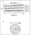
- the OD value was measured at a certain distance from the center position of each separation layer. The results are shown in Table 2 and FIG.
- OD value was measured in each position where the distance from the center in the separated layer on a support plate differs as shown in Table 2 and FIG. 4 (a) and (b).
- the distance from the center of the separation layer to 120 mm was 6 mm, and the distance from the center to 120 mm to 150 mm was 3 mm.
- an adhesive composition (TZNR-A3007, Tokyo Ohka Kogyo Co., Ltd.) was placed on the Sn-Ag plate of a 12-inch silicon wafer (substrate) equipped with a Sn-Ag plate (tin-silver plate, 0.3 to 0.4 ⁇ m). Company) was applied and baked at 100 ° C., 160 ° C., and 200 ° C. for 3 minutes each to form an adhesive layer (film thickness 50 ⁇ m) (adhesive layer forming step).
- the Sn—Ag plate was used in place of an element mounted on the wafer substrate, an electric circuit, or the like. And it bonded together with the glass support body which formed the fluorocarbon film
- the wavelength of the laser beam is 532 nm
- the diameter of the laser beam is 180 ⁇ m
- the distance between the centers of the irradiated regions in the laser pulse is 180 ⁇ m
- the scanning speed is 7200 mm / s
- the average output of the laser beam is 3.42 W
- the repetition frequency Laser light irradiation was performed at 40 kHz.
- the damage received by the Sn-Ag plate was visually confirmed with a microscope.
- damage was indicated, and when no laser beam spot was formed, no damage was indicated.
- Target: 2000A where the OD value was entirely lower than 0.30 damage was observed on the Sn-Ag plate in both positions (1) and (2).
- Target: 4500A slight damage was observed on the Sn-Ag plate at the position where the OD value of both (3) and (4) was 0.29, but the OD value was 0.30 or more and 1.00. No damage was observed on the Sn-Ag plate at the following positions.
- Target: 7000A with an OD value of 0.30 or more and 1.00 or less over the entire surface, no damage was observed on the Sn-Ag plate in both positions (5) and (6).
- each of the laminates using 12-inch silicon wafers (substrates) loaded with various materials was prepared, and the deposition time of the separation layer by the CVD method
- the CVD method By creating a support plate that forms separation layers showing different OD values, creating a laminate that combines the conditions, and irradiating laser light, the effect of laser light on each material was compared with the case of Sn-Ag plate.
- Materials used in place of the elements and electric circuits were Cu (1 ⁇ m), SiO 2 (1 ⁇ m), Al (0.2 ⁇ m), and polyimide (0.1 ⁇ m), and these were formed on a 12-inch silicon wafer (substrate). The attached one was used for evaluation. The same evaluation was performed on the bare silicon wafer and compared with the case of the Sn—Ag plate.
- a fluorocarbon film was formed on a 12-inch bare glass (support plate) by plasma CVD using C 4 F 8 as a reaction gas under the conditions of a flow rate of 400 sccm, a pressure of 700 mTorr, a high-frequency power of 2500 W, and a film formation temperature of 240 ° C. Separation layer forming step).
- the film thickness of the separation layer was set to 2000 mm (0.2 ⁇ m), 4500 mm (0.45 ⁇ m), and 7000 mm (0.7 ⁇ m), respectively, and the film formation time was changed under three conditions.
- a support plate (“direct” in Table 3 below) that does not form a separation layer was also prepared.
- an OD value at a fixed distance from the center position of each separation layer was measured using an X-Rite 310 (OD value measuring device, manufactured by X-Rite).
- the thickness target of the separation layer is 2000 mm
- the OD value is about 0.15
- the film thickness target is 4500 mm
- the OD value is about 0.30
- the film thickness target is 7000 mm
- the OD value is about It became 0.45.
- an adhesive composition (TZNR-A3007, manufactured by Tokyo Ohka Kogyo Co., Ltd.) is applied onto a 12-inch silicon wafer (substrate) with or without various materials, and 100 ° C. and 160 ° C. Then, each layer was baked at 200 ° C. for 3 minutes to form an adhesive layer (film thickness 50 ⁇ m) (adhesive layer forming step).
- the various substrates were bonded to various glass supports (having a fluorocarbon film) for 3 minutes under conditions of 220 ° C. and 4000 Kg under vacuum to form a laminate (lamination step).
- the wavelength of the laser beam is 532 nm
- the diameter of the laser beam is 180 ⁇ m
- the distance between the centers of the irradiated regions in the laser pulse is 180 ⁇ m
- the scanning speed is 7300 mm / s
- the average output of the laser beam is 3.42 W
- the repetition frequency Laser light irradiation was performed at 40 kHz.
- the results differed depending on the type of material mounted on the substrate. That is, the OD value necessary for avoiding damage to elements, electrical circuits, and the like on the substrate by the laser light differs depending on the substrate. However, by selecting an appropriate OD value according to the type of material mounted on the substrate, in any case, it is shown that damage to elements, electrical circuits, etc. on the substrate due to laser light can be avoided. It was done.
- the present invention can be suitably used, for example, in a manufacturing process of a miniaturized semiconductor device.
Landscapes
- Chemical & Material Sciences (AREA)
- Chemical Kinetics & Catalysis (AREA)
- Inorganic Chemistry (AREA)
- General Chemical & Material Sciences (AREA)
- Engineering & Computer Science (AREA)
- Materials Engineering (AREA)
- Mechanical Engineering (AREA)
- Metallurgy (AREA)
- Organic Chemistry (AREA)
- Laminated Bodies (AREA)
Description
本発明は、積層体、積層体の分離方法、および分離層の評価方法に関する。
近年、ICカード、携帯電話などの電子機器の薄型化、小型化、軽量化などが要求されている。これらの要求を満たすためには、組み込まれる半導体チップについても薄型の半導体チップを使用しなければならない。このため、半導体チップの基となるウエハ基板の厚さ(膜厚)は現状では125μm~150μmであるが、次世代のチップ用には25μm~50μmにしなければならないといわれている。したがって、上記の膜厚のウエハ基板を得るためには、ウエハ基板の薄板化工程が必要不可欠である。
ウエハ基板は、薄板化によって強度が低下するので、薄板化したウエハ基板の破損を防ぐために、製造プロセス中は、ウエハ基板にサポートプレートを貼り合わせた状態で自動搬送しながら、ウエハ基板上に回路等の構造物を実装する。そして、製造プロセス後に、ウエハ基板をサポートプレートから分離する。したがって、製造プロセス中は、ウエハ基板とサポートプレートとが強固に接着していることが好ましいが、製造プロセス後には、サポートプレートからウエハ基板を円滑に分離できることが好ましい。
ウエハ基板とサポートプレートとを強固に接着した場合、接着材料によっては、ウエハ基板上に実装した構造物を破損させることなく、ウエハ基板からサポートプレートを分離することは困難である。したがって、製造プロセス中にはウエハ基板とサポートプレートとの強固な接着を実現しつつ、製造プロセス後にはウエハ基板上に実装した素子を破損させることなく分離するという、非常に困難な仮止め技術の開発が求められている。
半導体ウエハに支持体を貼り合わせ、半導体ウエハを処理した後、支持体を分離するような半導体チップの製造方法として、特許文献1に記載のような方法が知られている。特許文献1に記載の方法においては、光透過性の支持体と半導体ウエハとを、支持体側に設けられた光熱変換層と接着剤層とを介して貼り合わせ、半導体ウエハを処理した後、支持体側から放射エネルギーを照射することによって光熱変換層を分解して、支持体から半導体ウエハを分離する。
特許文献1に記載のように、半導体ウエハから支持体を分離するとき、支持体側から放射エネルギーを照射すると、照射したレーザー光が光熱変換層から漏れることがある。そして、その漏れ光が半導体ウエハ等の基板、又は基板に実装された電気回路、表示素子等に到達し、これらに悪影響を及ぼすことがある。このような漏れ光を低減するための方法として、光熱変換層を厚膜化することが考えられるが、スループットの悪化及びコストの増大を招く。
本発明は、上記課題に鑑みてなされたものであり、製造プロセス中には基板と支持体との強固な接着を実現しつつ、製造プロセス後には光照射によって、容易に基板と支持体とを分離するとともに、光による基板表面への悪影響を好適に防止するための技術を提供することを主たる目的とする。
上記の課題を解決するために、本発明に係る積層体は、基板と、接着層と、光を吸収することにより変質する分離層と、光透過性の支持体とがこの順番に積層された積層体であって、該分離層のOD値が、0.20以上、1.00以下であることを特徴とする。
また、本発明に係る積層体の分離方法は、基板と、接着層と、OD値が0.20以上、1.00以下であり、光を吸収することにより変質する分離層と、光透過性の支持体とがこの順番に積層された積層体を分離する積層体の分離方法であって、該支持体を介して、該分離層に上記OD値から設定される繰り返し周波数および平均出力値を有するレーザー光を照射する照射工程と、該照射工程の後、該基板と該支持体とを分離する分離工程とを包含することを特徴とする。
また、本発明に係る分離層の評価方法は、基板と、接着層と、光を吸収することにより変質する分離層と、光透過性の支持体とがこの順番に積層された積層体の分離層を評価する分離層の評価方法であって、該分離層のOD値を測定する測定工程を包含することを特徴とする。
本発明によれば、製造プロセス中には基板と支持体との強固な接着を実現しつつ、製造プロセス後には光照射によって、容易に基板と支持体とを分離するとともに、光による基板への悪影響を防止できるという効果を奏する。
〔積層体〕
本発明の一実施形態に係る積層体は、基板と、接着層と、光を吸収することによって変質する分離層と、光透過性の支持体とがこの順番に積層された積層体であって、該分離層のOD値が、0.20以上、1.00以下である構成である。
本発明の一実施形態に係る積層体は、基板と、接着層と、光を吸収することによって変質する分離層と、光透過性の支持体とがこの順番に積層された積層体であって、該分離層のOD値が、0.20以上、1.00以下である構成である。
すなわち、本実施形態に係る積層体は、被支持基板、接着層、分離層、および支持体がこの順に積層されており、被支持基板は、接着層および分離層を介して支持体に仮止めされている。
図1を参照して、本実施形態に係る積層体を説明する。本実施形態の積層体は、被支持基板を支持体に仮止めした積層体として用いるのであれば、具体的な用途は特に限定されない。以下の説明では、ウエハサポートシステムにおいて利用される、半導体ウエハ(被支持基板)をサポートプレート(支持体)に対して仮止めした積層体を例に挙げる。図1中(1)に示すように、本実施形態に係る積層体1は、基板11、サポートプレート(支持体)12、接着層14および分離層16を備えている。
(基板)
基板11は、サポートプレート12に支持された状態で、薄化、実装等のプロセスに供されるものである。基板11としては、ウエハ基板に限定されず、薄いフィルム基板、フレキシブル基板等の任意の基板を使用できる。また、基板11における接着層14側の面には、電気回路等の電子素子の微細構造が形成されていてもよい。
基板11は、サポートプレート12に支持された状態で、薄化、実装等のプロセスに供されるものである。基板11としては、ウエハ基板に限定されず、薄いフィルム基板、フレキシブル基板等の任意の基板を使用できる。また、基板11における接着層14側の面には、電気回路等の電子素子の微細構造が形成されていてもよい。
(サポートプレート)
サポートプレート12は、基板11を支持する支持体であり、光透過性を有している。そのため、積層体1の外からサポートプレート12に向けて光が照射されたときに、当該光がサポートプレート12を通過して分離層16に到達する。また、サポートプレート12は、必ずしも全ての光を透過させる必要はなく、分離層16に吸収されるべき(所定の波長を有している)光を透過させることができればよい。
サポートプレート12は、基板11を支持する支持体であり、光透過性を有している。そのため、積層体1の外からサポートプレート12に向けて光が照射されたときに、当該光がサポートプレート12を通過して分離層16に到達する。また、サポートプレート12は、必ずしも全ての光を透過させる必要はなく、分離層16に吸収されるべき(所定の波長を有している)光を透過させることができればよい。
(分離層)
分離層16は、支持体を介して照射される光を吸収することによって変質する材料から形成されている層である。本明細書において、分離層16が「変質する」とは、分離層16を、わずかな外力を受けて破壊され得る状態、又は分離層16と接する層との接着力が低下した状態にさせる現象を意味する。光の吸収によって生じる分離層16の変質の結果として、分離層16は、光の照射を受ける前の強度又は接着性を失う。よって、わずかな外力を加える(例えば、サポートプレート12を持ち上げるなど)ことによって、分離層16が破壊されて、サポートプレート12と基板11とを容易に分離できる。
分離層16は、支持体を介して照射される光を吸収することによって変質する材料から形成されている層である。本明細書において、分離層16が「変質する」とは、分離層16を、わずかな外力を受けて破壊され得る状態、又は分離層16と接する層との接着力が低下した状態にさせる現象を意味する。光の吸収によって生じる分離層16の変質の結果として、分離層16は、光の照射を受ける前の強度又は接着性を失う。よって、わずかな外力を加える(例えば、サポートプレート12を持ち上げるなど)ことによって、分離層16が破壊されて、サポートプレート12と基板11とを容易に分離できる。
また、分離層16の変質は、吸収した光のエネルギーによる(発熱性又は非発熱性の)分解、架橋、立体配置の変化又は官能基の解離(そして、これらにともなう分離層の硬化、脱ガス、収縮又は膨張)等であり得る。分離層16の変質は、分離層16を構成する材料による光の吸収の結果として生じる。よって、分離層16の変質の種類は、分離層16を構成する材料の種類に応じて変化し得る。
分離層16は、サポートプレート12における、接着層14を介して基板11が貼り合わされる側の表面に設けられている。すなわち、分離層16は、サポートプレート12と接着層14との間に設けられている。
分離層16の厚さは、例えば、0.05~100μmであり、0.1~50μmがより好ましく、0.1~10μmがさらに好ましく、0.3~1μmであることが特に好ましい。分離層16の厚さが0.05~100μmの範囲内に収まっていれば、短時間の光の照射及び低エネルギーの光の照射によって、分離層16を所望のように変質させることができる。また、分離層16の厚さは、生産性の観点から1μm以下の範囲内に収まっていることが特に好ましい。
なお、積層体1において、分離層16とサポートプレート12との間に他の層がさらに形成されていてもよい。この場合、他の層は光を透過する材料から構成されていればよい。これによって、分離層16への光の入射を妨げることなく、積層体1に好ましい性質などを付与する層を、適宜追加できる。分離層16を構成している材料の種類によって、用い得る光の波長が異なる。よって、他の層を構成する材料は、すべての光を透過させる必要はなく、分離層16を構成する材料を変質させ得る波長の光を透過させることができる材料から適宜選択し得る。
また、分離層16は、光を吸収する構造を有する材料のみから形成されていることが好ましいが、本発明における本質的な特性を損なわない範囲において、光を吸収する構造を有していない材料を添加して、分離層16を形成してもよい。また、分離層16における接着層14に対向する側の面が平坦である(凹凸が形成されていない)ことが好ましく、これにより、分離層16の形成が容易に実施され、且つ接着層14との貼り付けにおいても均一に貼り付けることが可能となる。
分離層16は、以下に示すような分離層16を構成する材料を予めフィルム状に形成したものをサポートプレート12に貼り合わせて用いてもよいし、サポートプレート12上に分離層16を構成する材料を塗布してフィルム状に固化したものを用いてもよい。サポートプレート12上に分離層16を構成する材料を塗布する方法は、分離層16を構成する材料の種類に応じて、化学気相成長(CVD)法による堆積等の従来公知の方法から適宜選択できる。
分離層16は、レーザーから照射される光を吸収することによって変質するものであってもよい。すなわち、分離層16を変質させるために分離層16に照射される光は、レーザーから照射されたものであってもよい。分離層16に照射する光を発射するレーザーの例としては、YAGレーザー、ルビーレーザー、ガラスレーザー、YVO4レーザー、LDレーザー、ファイバーレーザー等の固体レーザー、色素レーザー等の液体レーザー、CO2レーザー、エキシマレーザー、Arレーザー、He-Neレーザー等の気体レーザー、半導体レーザー、自由電子レーザー等のレーザー光、及ぶ非レーザー光が挙げられる。分離層16に照射する光を発射するレーザーは、分離層16を構成している材料に応じて適宜選択することが可能であり、分離層16を構成する材料を変質させ得る波長の光を照射するレーザーを選択すればよい。
<光吸収性を有している構造をその繰返し単位に含んでいる重合体>
分離層16は、光吸収性を有している構造をその繰返し単位に含んでいる重合体を含有していてもよい。当該重合体は光の照射を受けて変質する。当該重合体の変質は、上記構造が照射された光を吸収することによって生じる。分離層16は、重合体の変質の結果として、光の照射を受ける前の強度又は接着性を失っている。よって、わずかな外力を加える(例えば、サポートプレート12を持ち上げるなど)ことによって、分離層16が破壊されて、サポートプレート12と基板11とを容易に分離できる。
分離層16は、光吸収性を有している構造をその繰返し単位に含んでいる重合体を含有していてもよい。当該重合体は光の照射を受けて変質する。当該重合体の変質は、上記構造が照射された光を吸収することによって生じる。分離層16は、重合体の変質の結果として、光の照射を受ける前の強度又は接着性を失っている。よって、わずかな外力を加える(例えば、サポートプレート12を持ち上げるなど)ことによって、分離層16が破壊されて、サポートプレート12と基板11とを容易に分離できる。
光吸収性を有している上記構造は、繰返し単位として当該構造を含んでいる重合体を、当該構造による光の吸収によって変質させる化学構造である。当該構造は、例えば、置換もしくは非置換のベンゼン環、縮合環又は複素環からなる共役π電子系を含んでいる化学部分である。より詳細には、当該構造は、カルド構造、又は上記重合体の側鎖に存在するベンゾフェノン構造、ジフェニルスルフォキシド構造、ジフェニルスルホン構造(ビスフェニルスルホン構造)、ジフェニル構造もしくはジフェニルアミン構造であり得る。上記構造が上記重合体の側鎖に存在する場合、当該構造は以下の式によって表され得る。

式中、Rはそれぞれ独立して、アルキル基、アリール基、ハロゲン、水酸基、ケトン基、スルホキシド基、スルホン基又はN(R1)(R2)であり(ここで、R1及びR2はそれぞれ独立して、水素原子又は炭素数1~5のアルキル基である)、Zは、存在しないか、又はCO-、-SO2-、-SO-若しくは-NH-であり、nは0又は1~5の整数である。
また、上記重合体は、例えば、以下の式のうち、(a)~(d)のいずれかによって表される繰返し単位を含んでいるか、(e)によって表されるか、又は(f)の構造をその主鎖に含んでいる。
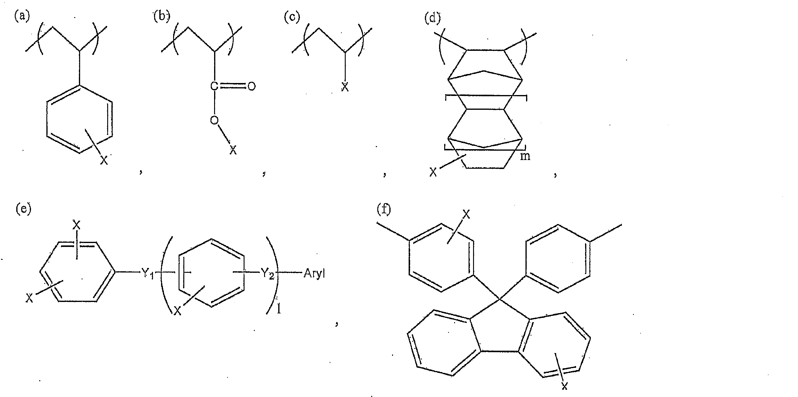
式中、lは1以上の整数であり、mは0又は1~2の整数であり、Xは、(a)~(e)において上記の“化1”に示した式のいずれかであり、(f)において上記の“化1”に示した式のいずれかであるか、又は存在せず、Y1及びY2はそれぞれ独立して、-CO-又はSO2-である。lは好ましくは10以下の整数である。
上記の“化1”に示されるベンゼン環、縮合環及び複素環の例としては、フェニル、置換フェニル、ベンジル、置換ベンジル、ナフタレン、置換ナフタレン、アントラセン、置換アントラセン、アントラキノン、置換アントラキノン、アクリジン、置換アクリジン、アゾベンゼン、置換アゾベンゼン、フルオリン、置換フルオリン、フルオリノン、置換フルオリン、カルバゾール、置換カルバゾール、N-アルキルカルバゾール、ジベンゾフラン、置換ジベンゾフラン、フェナンスレン、置換フェナンスレン、ピレン及び置換ピレンが挙げられる。例示した置換基が置換を有している場合、その置換基は、例えば、アルキル、アリール、ハロゲン原子、アルコキシ、ニトロ、アルデヒド、シアノ、アミド、ジアルキルアミノ、スルホンアミド、イミド、カルボン酸、カルボン酸エステル、スルホン酸、スルホン酸エステル、アルキルアミノ及びアリールアミノから選択される。
上記の“化1”に示される置換基のうち、フェニル基を2つ有している5番目の置換基であって、Zが-SO2-である場合の例としては、ビス(2,4‐ジヒドロキシフェニル)スルホン、ビス(3,4‐ジヒドロキシフェニル)スルホン、ビス(3,5‐ジヒドロキシフェニル)スルホン、ビス(3,6‐ジヒドロキシフェニル)スルホン、ビス(4‐ヒドロキシフェニル)スルホン、ビス(3‐ヒドロキシフェニル)スルホン、ビス(2‐ヒドロキシフェニル)スルホン、及びビス(3,5‐ジメチル‐4‐ヒドロキシフェニル)スルホンなどが挙げられる。
上記の“化1”に示される置換基のうち、フェニル基を2つ有している5番目の置換基であって、Zが-SO-である場合の例としては、ビス(2,3‐ジヒドロキシフェニル)スルホキシド、ビス(5‐クロロ‐2,3‐ジヒドロキシフェニル)スルホキシド、ビス(2,4‐ジヒドロキシフェニル)スルホキシド、ビス(2,4‐ジヒドロキシ‐6‐メチルフェニル)スルホキシド、ビス(5‐クロロ‐2,4‐ジヒドロキシフェニル)スルホキシド、ビス(2,5‐ジヒドロキシフェニル)スルホキシド、ビス(3,4‐ジヒドロキシフェニル)スルホキシド、ビス(3,5‐ジヒドロキシフェニル)スルホキシド、ビス(2,3,4‐トリヒドロキシフェニル)スルホキシド、ビス(2,3,4‐トリヒドロキシ‐6‐メチルフェニル)‐スルホキシド、ビス(5‐クロロ‐2,3,4‐トリヒドロキシフェニル)スルホキシド、ビス(2,4,6‐トリヒドロキシフェニル)スルホキシド、及びビス(5‐クロロ‐2,4,6‐トリヒドロキシフェニル)スルホキシドなどが挙げられる。
上記の“化1”に示される置換基のうち、フェニル基を2つ有している5番目の置換基であって、Zが-C(=O)-である場合の例としては、2,4‐ジヒドロキシベンゾフェノン、2,3,4‐トリヒドロキシベンゾフェノン、2,2’,4,4’‐テトラヒドロキシベンゾフェノン、2,2’,5,6’‐テトラヒドロキシベンゾフェノン、2‐ヒドロキシ‐4‐メトキシベンゾフェノン、2‐ヒドロキシ‐4‐オクトキシベンゾフェノン、2‐ヒドロキシ‐4‐ドデシルオキシベンゾフェノン、2,2’‐ジヒドロキシ‐4‐メトキシベンゾフェノン、2,6‐ジヒドロキシ‐4‐メトキシベンゾフェノン、2,2’‐ジヒドロキシ‐4,4’‐ジメトキシベンゾフェノン、4‐アミノ‐2’‐ヒドロキシベンゾフェノン、4‐ジメチルアミノ‐2’‐ヒドロキシベンゾフェノン、4‐ジエチルアミノ‐2’‐ヒドロキシベンゾフェノン、4‐ジメチルアミノ‐4’‐メトキシ‐2’‐ヒドロキシベンゾフェノン、4‐ジメチルアミノ‐2’,4’‐ジヒドロキシベンゾフェノン、及び4‐ジメチルアミノ‐3’,4’‐ジヒドロキシベンゾフェノンなどが挙げられる。
上記構造は、その種類の選択によって、所望の範囲の波長を有している光を吸収可能である。例えば、上記構造が吸収可能な光の波長は、100~2000nmであることがより好ましい。この範囲のうち、上記構造が吸収可能な光の波長は、より短波長側であり、例えば、100~500nmである。例えば、上記構造は、好ましくは約300~370nmの波長を有している紫外光を吸収することによって、当該構造を含んでいる重合体を変質させ得る。
上記構造が吸収可能な光は、例えば、高圧水銀ランプ(波長:254nm~436nm)、KrFエキシマレーザー(波長:248nm)、ArFエキシマレーザー(波長:193nm)、F2エキシマレーザー(波長:157nm)、XeClレーザー(308nm)、XeFレーザー(波長:351nm)若しくは固体UVレーザー(波長:355nm)から発せられる光、又はg線(波長:436nm)、h線(波長:405nm)若しくはi線(波長:365nm)などである。
上述した分離層16は、繰り返し単位として上記構造を含んでいる重合体を含有しているが、分離層16は、上記重合体以外の成分をさらに含み得る。当該成分としては、フィラー、可塑剤、及びサポートプレート12の剥離性を向上し得る成分などが挙げられる。これらの成分は、上記構造による光の吸収、及び重合体の変質を妨げないか、又は促進する、従来公知の物質又は材料から適宜選択される。
<無機物>
分離層16は、無機物から構成され得る。当該無機物は、光の吸収によって変質する材料である。このような無機物によって構成されている分離層16は、光の吸収によって変質し、光の照射を受ける前の強度又は接着性を失う。光の照射を受けた分離層16は、わずかな外力を受ける(例えば、サポートプレート12を持ち上げる等)ことによって破壊されるので、サポートプレート12と基板11とを容易に分離できる。
分離層16は、無機物から構成され得る。当該無機物は、光の吸収によって変質する材料である。このような無機物によって構成されている分離層16は、光の吸収によって変質し、光の照射を受ける前の強度又は接着性を失う。光の照射を受けた分離層16は、わずかな外力を受ける(例えば、サポートプレート12を持ち上げる等)ことによって破壊されるので、サポートプレート12と基板11とを容易に分離できる。
上記無機物は、光を吸収することによって変質する材料であればよく、当該無機物として、例えば、金属、金属化合物及びカーボンからなる群より選択される1種類以上の無機物を好適に用いることができる。金属化合物とは、金属原子を含む化合物を指し、例えば、金属酸化物、金属窒化物であり得る。このような無機物の例としては、これに限定されるものではないが、金、銀、銅、鉄、ニッケル、アルミニウム、チタン、クロム、SiO2、SiN、Si3N4、TiN、及びカーボンからなる群より選ばれる1種類以上の無機物が挙げられる。なお、カーボンとは炭素の同素体をも包含し得る概念であり、例えば、ダイヤモンド、フラーレン、ダイヤモンドライクカーボン、カーボンナノチューブ等であり得る。
上記無機物は、その種類によって固有の範囲の波長を有する光を吸収する。分離層16に用いた無機物が吸収する範囲の波長の光を分離層に照射することによって、上記無機物を好適に変質させ得る。
無機物からなる分離層16に照射する光として、上記無機物が吸収可能な波長に応じて、例えば、YAGレーザー、ルビーレーザー、ガラスレーザー、YVO4レーザー、LDレーザー、ファイバーレーザー等の固体レーザー、色素レーザー等の液体レーザー、CO2レーザー、エキシマレーザー、Arレーザー、He-Neレーザー等の気体レーザー、半導体レーザー、自由電子レーザー等のレーザー光、又は非レーザー光を適宜用いればよい。
無機物からなる分離層16は、例えばスパッタ、化学蒸着(CVD)、メッキ、プラズマCVD、スピンコート等の公知の技術によって、サポートプレート12上に形成され得る。無機物からなる分離層16の厚さは特に限定されず、使用する光を十分に吸収し得る膜厚であればよいが、例えば、0.05~10μmの膜厚とすることがより好ましい。また、分離層16を構成する無機物からなる無機膜(例えば、金属膜)の両面又は片面に予め接着剤を塗布し、サポートプレート12及び基板11に貼り付けてもよい。
なお、分離層16として金属膜を使用する場合には、分離層16の膜質、レーザー光源の種類、レーザー出力等の条件によっては、レーザーの反射や膜への帯電等が起こり得る。そのため、反射防止膜や帯電防止膜を分離層16の上、下又はどちらか一方に設けることで、それらの対策をとることが好ましい。
<赤外線吸収性の構造を有する化合物>
分離層16は、赤外線吸収性の構造を有する化合物によって形成されていてもよい。当該化合物は、赤外線を吸収することにより変質する。分離層16は、化合物の変質の結果として、赤外線の照射を受ける前の強度又は接着性を失っている。よって、わずかな外力を加える(例えば、サポートプレートを持ち上げるなど)ことによって、分離層16が破壊されて、サポートプレート12と基板11とを容易に分離できる。
分離層16は、赤外線吸収性の構造を有する化合物によって形成されていてもよい。当該化合物は、赤外線を吸収することにより変質する。分離層16は、化合物の変質の結果として、赤外線の照射を受ける前の強度又は接着性を失っている。よって、わずかな外力を加える(例えば、サポートプレートを持ち上げるなど)ことによって、分離層16が破壊されて、サポートプレート12と基板11とを容易に分離できる。
赤外線吸収性を有している構造又は赤外線吸収性を有している構造を含む化合物としては、たとえば、アルカン、アルケン(ビニル、トランス、シス、ビニリデン、三置換、四置換、共役、クムレン、環式)、アルキン(一置換、二置換)、単環式芳香族(ベンゼン、一置換、二置換、三置換)、アルコール及びフェノール類(自由OH、分子内水素結合、分子間水素結合、飽和第二級、飽和第三級、不飽和第二級、不飽和第三級)、アセタール、ケタール、脂肪族エーテル、芳香族エーテル、ビニルエーテル、オキシラン環エーテル、過酸化物エーテル、ケトン、ジアルキルカルボニル、芳香族カルボニル、1,3-ジケトンのエノール、o-ヒドロキシアリールケトン、ジアルキルアルデヒド、芳香族アルデヒド、カルボン酸(二量体、カルボン酸アニオン)、ギ酸エステル、酢酸エステル、共役エステル、非共役エステル、芳香族エステル、ラクトン(β-、γ-、δ-)、脂肪族酸塩化物、芳香族酸塩化物、酸無水物(共役、非共役、環式、非環式)、第一級アミド、第二級アミド、ラクタム、第一級アミン(脂肪族、芳香族)、第二級アミン(脂肪族、芳香族)、第三級アミン(脂肪族、芳香族)、第一級アミン塩、第二級アミン塩、第三級アミン塩、アンモニウムイオン、脂肪族ニトリル、芳香族ニトリル、カルボジイミド、脂肪族イソニトリル、芳香族イソニトリル、イソシアン酸エステル、チオシアン酸エステル、脂肪族イソチオシアン酸エステル、芳香族イソチオシアン酸エステル、脂肪族ニトロ化合物、芳香族ニトロ化合物、ニトロアミン、ニトロソアミン、硝酸エステル、亜硝酸エステル、ニトロソ結合(脂肪族、芳香族、単量体、二量体)、メルカプタン及びチオフェノール及びチオール酸などの硫黄化合物、チオカルボニル基、スルホキシド、スルホン、塩化スルホニル、第一級スルホンアミド、第二級スルホンアミド、硫酸エステル、炭素-ハロゲン結合、Si-A1結合(A1は、H、C、O又はハロゲン)、P-A2結合(A2は、H、C又はO)、又はTi-O結合であり得る。
上記炭素-ハロゲン結合を含む構造としては、例えば、-CH2Cl、-CH2Br、-CH2I、-CF2-、-CF3、-CH=CF2、-CF=CF2、フッ化アリール、及び塩化アリールなどが挙げられる。
上記Si-A1結合を含む構造としては、SiH、SiH2、SiH3、Si-CH3、Si-CH2-、Si-C6H5、SiO脂肪族、Si-OCH3、Si-OCH2CH3、Si-OC6H5、Si-O-Si、Si-OH、SiF、SiF2、及びSiF3などが挙げられる。Si-A1結合を含む構造としては、特に、シロキサン骨格及びシルセスキオキサン骨格を形成していることが好ましい。
上記P-A2結合を含む構造としては、PH、PH2、P-CH3、P-CH2-、P-C6H5、A3
3-P-O(A3は脂肪族又は芳香族)、(A4O)3-P-O(A4はアルキル)、P-OCH3、P-OCH2CH3、P-OC6H5、P-O-P、P-OH、及びO=P-OHなどが挙げられる。
上記構造は、その種類の選択によって、所望の範囲の波長を有している赤外線を吸収可能である。たとえば、上記構造が吸収可能な赤外線の波長は、例えば1μm~20μmの範囲内であり、2μm~15μmの範囲内をより好適に吸収できる。さらに、上記構造がSi-O結合、Si-C結合及びTi-O結合である場合には、9μm~11μmの範囲内であり得る。なお、各構造が吸収できる赤外線の波長は、当業者によって容易に理解される。例えば、各構造における吸収帯として、非特許文献:SILVERSTEIN・BASSLER・MORRILL著「有機化合物のスペクトルによる同定法(第5版)-MS、IR、NMR、UVの併用-」(1992年発行)第146頁~第151頁の記載を参照すればよい。
分離層16の形成に用いられる、赤外線吸収性の構造を有する化合物としては、上述のような構造を有している化合物のうち、塗布のために溶媒に溶解でき、固化されて固層を形成できるものであれば、特に限定されるものではない。
一例を挙げて説明すれば、シロキサン骨格を有する化合物として、例えば、下記式(1)によって表される繰り返し単位及び下記式(2)によって表される繰り返し単位の共重合体である樹脂、あるいは下記式(1)によって表される繰り返し単位及びアクリル系化合物由来の繰り返し単位の共重合体である樹脂を用いることができる。
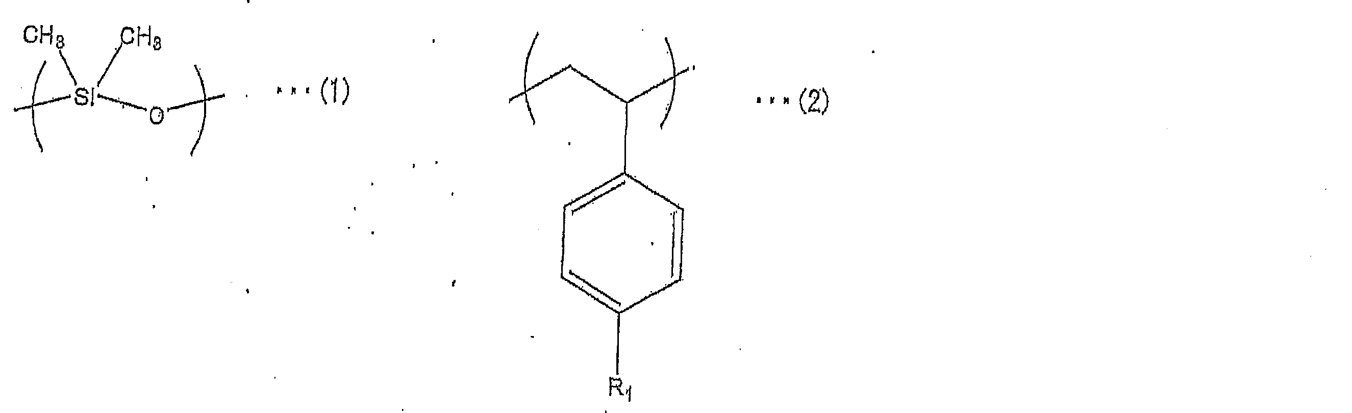
(式(2)中、R1は、水素、炭素数10以下のアルキル基、炭素数10以下のアルコキシ基である)
中でも、シロキサン骨格を有する化合物としては、上記式(1)によって表される繰り返し単位及び下記式(3)によって表される繰り返し単位の共重合体であるtert-ブチルスチレン(TBST)-ジメチルシロキサン共重合体がより好ましく、上記式(1)によって表される繰り返し単位及び下記式(3)によって表される繰り返し単位を1:1で含む、TBST-ジメチルシロキサン共重合体がさらに好ましい。
中でも、シロキサン骨格を有する化合物としては、上記式(1)によって表される繰り返し単位及び下記式(3)によって表される繰り返し単位の共重合体であるtert-ブチルスチレン(TBST)-ジメチルシロキサン共重合体がより好ましく、上記式(1)によって表される繰り返し単位及び下記式(3)によって表される繰り返し単位を1:1で含む、TBST-ジメチルシロキサン共重合体がさらに好ましい。

また、シルセスキオキサン骨格を有する化合物として、たとえば、下記式(4)によって表される繰り返し単位及び下記式(5)によって表される繰り返し単位の共重合体である樹脂を用いることができる。

(式(4)中、R2は、水素又は炭素数1以上、10以下のアルキル基であり、式(5)中、R3は、炭素数1以上、10以下のアルキル基、又はフェニル基である)
シルセスキオキサン骨格を有する化合物として、このほかにも、特許文献3:特開2007-258663号公報(2007年10月4日公開)、特許文献4:特開2010-120901号公報(2010年6月3日公開)、特許文献5:特開2009-263316号公報(2009年11月12日公開)及び特許文献6:特開2009-263596号公報(2009年11月12日公開)において開示されている各シルセスキオキサン樹脂を好適に利用できる。
シルセスキオキサン骨格を有する化合物として、このほかにも、特許文献3:特開2007-258663号公報(2007年10月4日公開)、特許文献4:特開2010-120901号公報(2010年6月3日公開)、特許文献5:特開2009-263316号公報(2009年11月12日公開)及び特許文献6:特開2009-263596号公報(2009年11月12日公開)において開示されている各シルセスキオキサン樹脂を好適に利用できる。
中でも、シルセスキオキサン骨格を有する化合物としては、下記式(6)によって表される繰り返し単位及び下記式(7)によって表される繰り返し単位の共重合体がより好ましく、下記式(6)によって表される繰り返し単位及び下記式(7)によって表される繰り返し単位を、7:3の比率において含む共重合体がさらに好ましい。
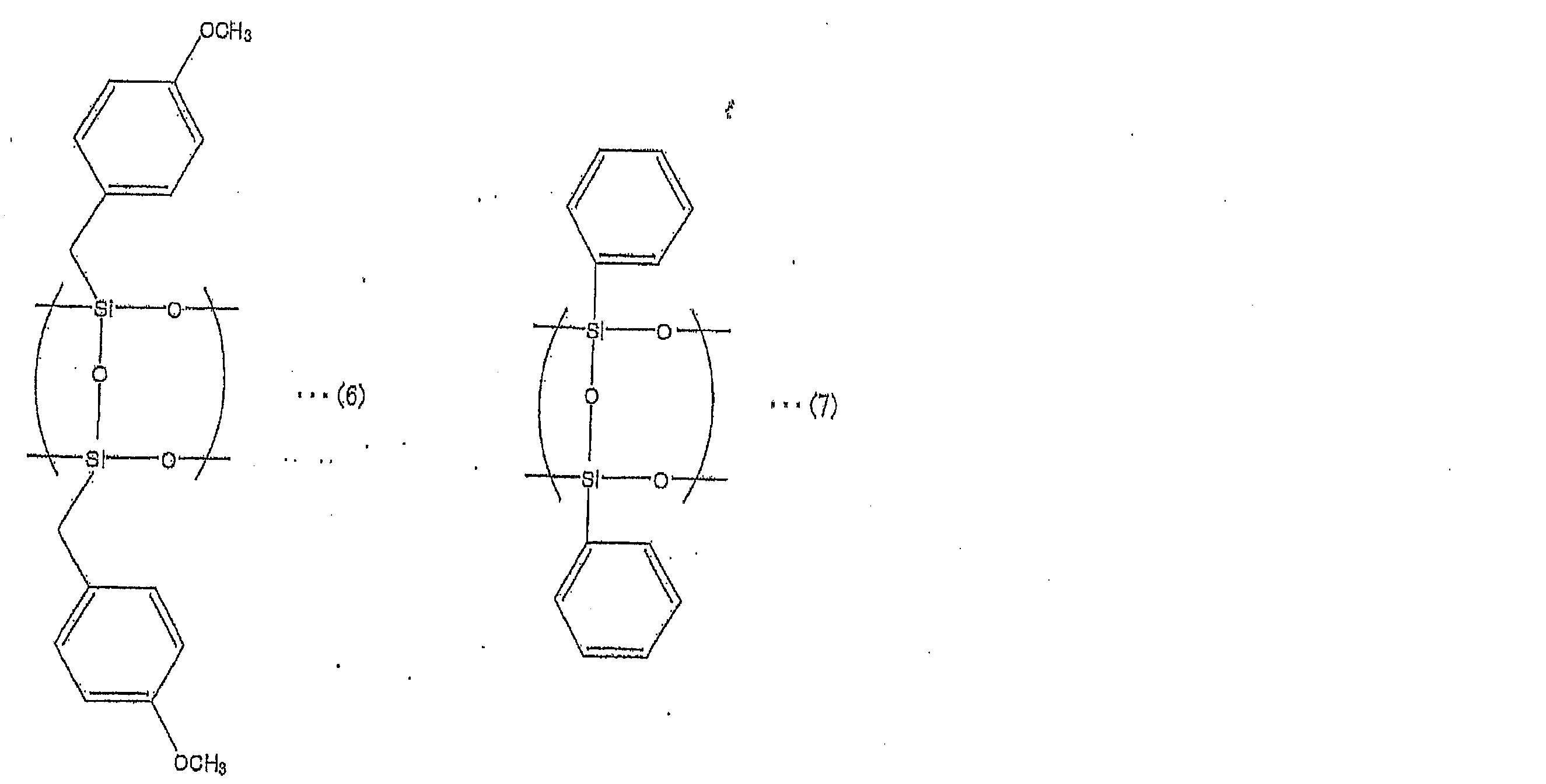
シルセスキオキサン骨格を有する重合体としては、ランダム構造、ラダー構造、及び籠型構造があり得るが、何れの構造であってもよい。
また、Ti-O結合を含む化合物としては、たとえば、(i)テトラ-i-プロポキシチタン、テトラ-n-ブトキシチタン、テトラキス(2-エチルヘキシルオキシ)チタン、及びチタニウム-i-プロポキシオクチレングリコレートなどのアルコキシチタン、(ii)ジ-i-プロポキシ・ビス(アセチルアセトナト)チタン、及びプロパンジオキシチタンビス(エチルアセトアセテート)などのキレートチタン、(iii)i-C3H7O-[-Ti(O-i-C3H7)2-O-]n -i-C3H7、及びn-C4H9O-[Ti(O-n-C4H9)2-O-]n-n-C4H9などのチタンポリマー、(iv)トリ-n-ブトキシチタンモノステアレート、チタニウムステアレート、ジ-i-プロポキシチタンジイソステアレート、及び(2-n-ブトキシカルボニルベンゾイルオキシ)トリブトキシチタンなどのアシレートチタン、(v)ジ-n-ブトキシ・ビス(トリエタノールアミナト)チタンなどの水溶性チタン化合物などが挙げられる。
中でも、Ti-O結合を含む化合物としては、ジ-n-ブトキシ・ビス(トリエタノールアミナト)チタン(Ti(OC4H9)2[OC2H4N(C2H4OH)2]2)が好ましい。
上述した分離層16は、赤外線吸収性の構造を有する化合物を含有しているが、分離層16は、上記化合物以外の成分をさらに含み得る。当該成分としては、フィラー、可塑剤、及びサポートプレート12の剥離性を向上し得る成分などが挙げられる。これらの成分は、上記構造による赤外線の吸収、及び化合物の変質を妨げないか、又は促進する、従来公知の物質又は材料から適宜選択される。
<フルオロカーボン>
分離層16は、フルオロカーボンから構成され得る。フルオロカーボンは光の吸収によって変質する。フルオロカーボンによって構成されている分離層16は、光の吸収によって変質し、光の照射を受ける前の強度又は接着性を失う。光の照射を受けた分離層16は、わずかな外力を受ける(例えば、サポートプレート12を持ち上げるなど)ことによって破壊されるので、サポートプレート12と基板11とを容易に分離できる。
分離層16は、フルオロカーボンから構成され得る。フルオロカーボンは光の吸収によって変質する。フルオロカーボンによって構成されている分離層16は、光の吸収によって変質し、光の照射を受ける前の強度又は接着性を失う。光の照射を受けた分離層16は、わずかな外力を受ける(例えば、サポートプレート12を持ち上げるなど)ことによって破壊されるので、サポートプレート12と基板11とを容易に分離できる。
また、一つの観点からいえば、分離層16を構成するフルオロカーボンは、プラズマCVD法によって好適に成膜され得る。なお、フルオロカーボンは、CxFy(パーフルオロカーボン)及びCxHyFz(x、y及びzは正の整数)を含み、これらに限定されないが、例えば、CHF3、CH2F2、C2H2F2、C4F8、C2F6、C5F8等で有り得る。また、分離層16を構成するために用いるフルオロカーボンに対して、必要に応じて窒素、ヘリウム、アルゴン等の不活性ガス、酸素、アルカン、アルケンなどの炭化水素、及び、二酸化炭素、水素を添加してもよい。また、これらのガスを複数混合して用いてもよい(フルオロカーボン、水素、窒素の混合ガス等)。また、分離層16は、単一種のフルオロカーボンから構成されていてもよいし、2種類以上のフルオロカーボンから構成されていてもよい。
フルオロカーボンは、その種類によって固有の範囲の波長を有する光を吸収する。分離層16に用いたフルオロカーボンが吸収する範囲の波長の光を分離層に照射することによって、フルオロカーボンを好適に変質させ得る。
分離層16に照射する光としては、フルオロカーボンが吸収可能な波長に応じて、例えば、YAGレーザー、ルビーレーザー、ガラスレーザー、YVO4レーザー、LDレーザー、ファイバーレーザー等の固体レーザー、色素レーザー等の液体レーザー、CO2レーザー、エキシマレーザー、Arレーザー、He-Neレーザー等の気体レーザー、半導体レーザー、自由電子レーザー等のレーザー光、又は非レーザー光を適宜用いればよい。フルオロカーボンを変質させ得る波長として、これに限定されるものではないが、例えば、600nm以下の範囲のものを用いることができる。
<赤外線吸収物質>
分離層16は、赤外線吸収物質を含有していてもよい。赤外線吸収物質は光の吸収によって変質する材料である。赤外線吸収物質を含有して構成されている分離層16は、光の吸収によって変質し、光の照射を受ける前の強度又は接着性を失う。光の照射を受けた分離層16は、わずかな外力を受ける(例えば、サポートプレート12を持ち上げる等)ことによって破壊されるので、サポートプレート12と基板11とを容易に分離できる。
分離層16は、赤外線吸収物質を含有していてもよい。赤外線吸収物質は光の吸収によって変質する材料である。赤外線吸収物質を含有して構成されている分離層16は、光の吸収によって変質し、光の照射を受ける前の強度又は接着性を失う。光の照射を受けた分離層16は、わずかな外力を受ける(例えば、サポートプレート12を持ち上げる等)ことによって破壊されるので、サポートプレート12と基板11とを容易に分離できる。
赤外線吸収物質は、赤外線を吸収することによって変質する材料であればよく、当該赤外線吸収物質として、例えば、カーボンブラック、鉄粒子、又はアルミニウム粒子を好適に用いることができる。赤外線吸収物質は、その種類によって固有の範囲の波長を有する光を吸収する。分離層16に用いた赤外線吸収物質が吸収する範囲の波長の光を分離層16に照射することによって、赤外線吸収物質を好適に変質させ得る。
<反応ガスを用いたプラズマ処理によって形成される層>
分離層16は、反応ガスを用いたプラズマ処理によって形成される層であり得る。当該反応ガスは、不飽和結合を有する有機化合物とフッ素化合物を含有していることが好ましい。
分離層16は、反応ガスを用いたプラズマ処理によって形成される層であり得る。当該反応ガスは、不飽和結合を有する有機化合物とフッ素化合物を含有していることが好ましい。
当該有機化合物としては、不飽和結合を有するものであればよく、例えば、アルケン、シクロアルケン、アルキン、及び芳香族化合物を挙げることができる。ここで、アルケンとしては、例えば、1,2-ブタジエン、1,3-ブタジエン、2,3-ジメチル-1,3-ブタジエン、3-メチル-1,2-ブタジエン、イソプレン、等を挙げることができる。又、シクロアルケンとしては、例えば、1,3-ヘキサジエン、1,4-ヘキサジエン、シクロペンタジエン、1,5-シクロオクタジエン、等を挙げることができる。又、アルキンとしては、例えば、アセチレン等を挙げることができる。又、芳香族化合物しては、ベンゼン、トルエン、キシレン、スチレン等を挙げることができる。又、不飽和結合を有していれば、例えば、エーテル結合、エステル結合、及びシロキシ結合等を有する有機化合物を用いることもできる。エーテル結合及び/又はシロキシ結合を有する有機化合物としては、例えば、1-メトキシ-3-(トリメチルシリルオキシ)-1,3-ブタジエン、及び2-トリメチルシリルオキシ-1,3-ブタジエン等を挙げることができる。又、エステル結合を有する有機化合物としては、例えば、2,3-ブタジエン酸エチル等を挙げることができる。又、これら有機化合物は、2種類以上混合して用いてもよい。これら有機化合物をプラズマ処理の反応ガスとして用いることによって、分離層16に不飽和結合を導入することができる。これによって、高密度プラズマのみならず低密度プラズマにおいても、光を吸収することによって変質する分離層16を形成することが可能になる。
ここで、有機化合物は、アルケン又はシクロアルケンであることが好ましい。アルケン又はシクロアルケンは、低密度プラズマによって崩壊しにくい構造を有している。このため、反応ガスにアルケン又はシクロアルケンを含有させることで、プラズマ処理においアルケン又はシクロアルケンを過剰に崩壊させることなく好適に重合させることができる。又、プラズマ処理によって形成される分離層16に不飽和結合を導入することができる。従って、有機化合物としてアルケン又はシクロアルケンを用いることで、光を吸収することによって変質する分離層16を好適に形成することができる。
又、有機化合物は不飽和結合が2つ以上あることが好ましい。これにより、さらに好適に光を吸収することができる分離層16を形成することができる。
又、有機化合物は、沸点が30℃以上、100℃以下の範囲内であることが好ましく、30℃以上、60℃以下の範囲内であることがさらに好ましく、40℃以上、50℃以下の範囲内であることが最も好ましい。有機化合物の沸点が、30℃以上、100℃以下の範囲内であれば、プラズマ処理のための条件において、反応ガスとして有機化合物を好適に使用することができる。
本実施形態に係る積層体の製造方法において用いる反応ガスが含有するフッ素化合物としては、例えば、フルオロカーボン、4フッ化炭素(CF4)、3フッ化窒素(NF3)及び6フッ化硫黄(SF6)等を挙げることができる。フルオロカーボンとしては、例えば、C4F8等を挙げることができる。反応ガスにフッ素化合物を含有することによって、分離層16の脆さを改善することができ、分離層16の耐薬品性を向上することができる。ここで、フッ素化合物は、フッ素化合物は、6フッ化硫黄(SF6)であることが特に好ましい。反応ガスに6フッ化硫黄(SF6)を含有させることによって、分離層16の脆さをさらに改善することができ、耐薬品性の良い分離層16を好適に形成することができる。
(プラズマ処理)
プラズマ処理に用いるプラズマ処理装置としては、特に限定されず、公知のプラズマ処理装置を用いることができる。
プラズマ処理に用いるプラズマ処理装置としては、特に限定されず、公知のプラズマ処理装置を用いることができる。
プラズマ処理装置が備える電極は、特に限定されず、例えば、デュアルコイルアンテナ、シングルコイルアンテナ、又は平行平板電極であってもよいが、平行平板電極を用いることにより、支持体上に形成する分離層16の表面積をより大きくすることが可能になり、その結果、直径のより大きい基板を用いて積層体を製造することが可能になる。
プラズマ処理装置の反応室の形状は、特に限定されず、ドーム型であってもよいし、円筒型等のその他の形状であってもよい。反応室のサイズは、処理対象の基板のサイズに応じて適宜選択すればよい。又、反応室の材質は、プラズマ処理及び分離層16の形成を阻害しない公知の材料を適宜選択することができる。
プラズマ処理装置において生じるプラズマには、コイル電極又は平行平板電極に印加される高周波電力による静電界による容量結合プラズマ(CCP:Conductive Coupled Plasma)とコイル電極に流れる高周波電流により発生する誘導電界による誘導結合プラズマ(ICP:Inductive Coupled Plasma)とが存在する。
本実施形態において、分離層形成工程のプラズマ処理は、低密度プラズマ処理であることが好ましい。ここで、低密度プラズマとは、イオン密度が1×1010cm-3以下であるプラズマであり、容量結合主体のプラズマのことをいう。分離層形成工程のプラズマ処理として低密度プラズマ処理を採用することによって、プラズマ処理装置の大型化が容易になる。このため、支持体上に形成する分離層16の表面積をより大きくすることが可能になる。従って、積層する基板の大型化が可能になる。
図2を用いて、本発明の一実施形態に係る積層体の製造方法が包含する分離層形成工程について、より詳細に説明する。図2は、本発明の一実施形態に係る製造方法が包含する分離層製造工程について説明する模式図である。
図2に示す通り、本実施形態に係る積層体の製造方法が包含する分離層形成工程に用いるプラズマ処理装置100は、反応室101内に、一対の平行平板電極102、サポートプレート12を戴置するステージ103を備えている。ここで、プラズマ処理装置100は、配管116aによって液体マスフローコントローラ112及び気化器113を経るようにして、有機化合物を貯留した容器111と連通しており、配管116bによってマスフローコントローラ115を経るようにして、フッ素化合物ボンベ114に連通している。又、配管116aと116bとは、配管116に合流している。
反応室101は、プラズマ処理により、反応ガスから分離層16を形成するために用いられる。又、反応室101は、真空ポンプ(図示せず)によって、反応室101内の圧力を調整できるようになっている。
一対の平行平板電極102は、反応室101内に設けられており、高周波電力を印加することによって反応ガスを用いてプラズマを発生させる。
ステージ103は、一対の平行平板電極102の一方を備えており、サポートプレート12を戴置できるようになっている。
容器111は、反応ガスに用いる有機化合物を貯留しており、窒素加圧することによって、配管116aを介して有機化合物を液体マスフローコントローラ112に供給する。
液体マスフローコントローラ112は、有機化合物の流量を調整する装置であり、配管116aを介して気化器113に供給する有機化合物の流量を調整する。
フッ素化合物ボンベ114は、反応ガスに用いるフッ素化合物を貯留しているボンベであり、配管116bを介して、フッ素ガスをマスフローコントローラ115に供給する。
マスフローコントローラ115は、フッ素ガスの流量を調整する装置であり、配管116bを介して供給されたフッ素ガスの流量を調整する。
配管116aと配管116bとは、配管116に合流する。ここで、配管116は加熱されることによって、反応ガスの液化を防止できるようになっている。
図2に示す通り、分離層形成工程では、反応室101内において、一対の平行平板電極102の一方を備えたステージ103の上にサポートプレート12を戴置する。ここで、反応室101内とサポートプレート12とを予備加熱する予備加熱工程を行ってもよい。
又、予備処理においては、予備処理ガスに酸素ガスを含有させることによって、サポートプレート12の表面をクリーニングしてもよい。
分離層形成工程では、反応室101内に分離層16となる反応ガスを供給して、プラズマ処理によりサポートプレート12に分離層16を形成する。ここで、反応ガスに含有されている有機化合物は、容器111から供給され、液体マスフローコントローラ112によって流量を調整され、気化器113によって気化される。又、フッ素化合物は、フッ素化合物ボンベ114から供給され、マスフローコントローラ115によって流量を調整される。その後、気化した有機化合物とフッ素化合物は配管116において混合され、加熱されつつ反応室101内に供給される。
液体マスフローコントローラ112及びマスフローコントローラ115によって有機化合物及びフッ素ガスの流量を調整することで、反応ガスが含有する有機化合物とフッ素化合物との体積比を調整することができる。例えば、有機化合物とフッ素化合物との体積比が6:4~9:1であれば、脆さがなく、耐薬品性の良い分離層16を形成することができる。又、サポートプレートを介して光を照射した後に、洗浄液によって好適に除去可能な分離層16を形成することができる。又、分離層形成工程の最中において、有機化合物とフッ素化合物の体積比を調整することもできる。
また、反応ガスには、窒素、ヘリウム、アルゴン等の不活性ガス、水素、酸素等の添加ガスを1種類以上添加してもよい。
反応室101内の目標温度は、特に限定されず、公知の温度を用いることができるが、100℃以上、300℃以下の範囲内であることがより好ましく、200℃以上、250℃以下の範囲内であることが特に好ましい。反応室内の温度を、このような範囲に設定することにより、プラズマ処理を好適に実行することができる。
分離層形成工程において形成される分離層16の厚さは特に限定されず、使用する光を十分に吸収し得る膜厚であればよいが、例えば、0.5μm以上、2.0μm以下の範囲内の膜厚とすることがより好ましく、1.0μm以上、1.5以下の範囲内の膜厚とすることが特に好ましい。分離層形成工程における分離層16の形成時間は、形成する膜厚に応じて設定すればよい。
<多層からなる分離層の例>
分離層16は、図3に示すように、第1の分離層16aおよび第2の分離層16bからなり得る。積層体20は、分離層16が2層である点を除いて、積層体1と同様の構成を有している。ここで、第1の分離層16aは、不飽和結合を有する有機化合物とフッ素化合物を含有している反応ガスを用いて、図2のプラズマ処理装置100によって形成されている。第2の分離層16bは、第1の分離層16aに該当しない、本明細書において例示されている光の照射によって変質する材料によって形成されている層である。
分離層16は、図3に示すように、第1の分離層16aおよび第2の分離層16bからなり得る。積層体20は、分離層16が2層である点を除いて、積層体1と同様の構成を有している。ここで、第1の分離層16aは、不飽和結合を有する有機化合物とフッ素化合物を含有している反応ガスを用いて、図2のプラズマ処理装置100によって形成されている。第2の分離層16bは、第1の分離層16aに該当しない、本明細書において例示されている光の照射によって変質する材料によって形成されている層である。
上記の構成によって、一実施形態に係る積層体20は、第1の分離層16aと第2分離層16bとが支持体上に形成されている。ここで、第1の分離層16aは様々な薬品処理における耐薬品性を備えており、第2の分離層16bは光を照射した後の良好な分離性を備えている。例えば、第2の分離層の16b上に第1の分離層16aがある場合、第2の分離層16bが薬品処理によって変質することを第1の分離層16aによって防止できる。逆に、第1の分離層16aの上に第2の分離層16bがある場合、第2の分離層16bが薬品処理によって変質しても、第1の分離層16aによって分離層としての機能を確保できる。又、支持体を介して分離層に光を照射することによって、分離層を好適に変質することができ、積層体から基板を容易に分離することができる。
(光学濃度)
一般には、光学濃度(以下、OD値という)は以下の式(1)で求められる。
一般には、光学濃度(以下、OD値という)は以下の式(1)で求められる。
D=-log(I/I0)・・・(1)
ここで、DはOD値であり、Iは入射光の強度であり、I0は透過光の強度である。
ここで、DはOD値であり、Iは入射光の強度であり、I0は透過光の強度である。
本実施形態においては、分離層16のOD値は、X-Rite310(OD値測定機:エックスライト社製)を用いて測定したOD値に基づき分離層16の評価を行う。
積層体1の分離層16のOD値は、0.20以上、1.00以下であることが好ましく、0.30以上、1.00以下であることがより好ましい。分離層16のOD値が0.20以上、1.00以下の範囲(特に、0.30以上、1.00以下の範囲、以下同様)において、基板11がダメージを受けないようにレーザー光を照射し得るとともに、分離層16の成膜時間を短縮し得ることを本発明者らは見出した。
特に、以下の条件において、基板11へのダメージを好適に防ぐことができる。言い換えれば、分離層16のOD値を、0.20以上、1.00以下としたとき、レーザー光の照射条件は、以下のように設定することが好ましい。
すなわち、レーザー光の平均出力値は、1.0W以上、5.0W以下の範囲であることが好ましく、3.0W以上、4.0W以下の範囲であることがより好ましい。また、レーザー光の繰り返し周波数は、20kHz以上、60kHz以下の範囲であることが好ましく、30kHz以上、50kHz以下の範囲であることがより好ましい。また、レーザー光の波長は、300nm以上、700nm以下であることが好ましく、450nm以上、650nm以下の範囲であることがより好ましい。このような条件によれば、分離層16に照射するパルス光のエネルギーを、基板11へのダメージを防ぎつつ、分離層16を変質させるための適切な条件にすることができる。
また、上記分離層16の分離工程に使用されるパルス光のビームスポット径は、100μm以上、250μm以下であることが好ましく、120μm以上、230μm以下であることがより好ましい。
また、パルス光の照射ピッチは、隣接するビームスポットが重ならず、かつ分離層16を変質させることが可能なピッチであればよいが、110μm以上、250μm以下であることが好ましく、160μm以上、220μm以下であることがより好ましい。
さらに、パルス光の照射速度は、分離層16を変質させることが可能な速度であればよいが、4000mm/s以上、10000mm/s以下であることが好ましく、5000mm/s以上、8000mm/s以下であることがより好ましい。
上記条件とすることで、レーザー光のビームスポットの重複が回避される。つまり、分離層16へ照射されるレーザー光のエネルギーの機械的側面からのばらつき(レーザー装置の設定によるばらつき)を制御できる。従って、OD値が規定された本実施形態に係る積層体に対し用いるレーザー光の照射条件として、好適に用いることができる。
さらに、分離層16に照射するパルス光のパルス幅は、20ナノ秒以上であることが好ましい。より好ましくは、40ナノ秒以上であり、さらに好ましくは、70ナノ秒以上である。分離層16に照射するパルス光のパルス幅の上限値は、200ナノ秒であることが好ましく、150ナノ秒であることがより好ましい。これにより、分離層16に吸収されずに漏れた光が、基板11及び基板11に形成された電子素子に及ぼす悪影響を、より抑えることができる。
分離層16のOD値は、分離層16を構成する材料の種類によって変化する。また、例えば、化学気相成長(CVD)法によって分離層16を成膜する場合、分離層16を構成する材料の密度によっても変化する。この場合、化学気相成長(CVD)法による分離層16の成膜時間、原料ガスの注入速度等を変更することによって、分離層16の密度を調整できる。
また、分離層16は、光を吸収する構造を有する材料のみから形成されていることが好ましいが、本発明における本質的な特性を損なわない範囲において、光を吸収する構造を有していない材料を添加して、OD値を調整することもできる。
(接着層)
接着層14は、基板11をサポートプレート12に接着固定すると同時に、基板11の表面を覆って保護する構成である。よって、接着層は、基板11の加工又は搬送の際に、サポートプレート12に対する基板11の固定、及び基板11の保護すべき面の被覆を維持する接着性及び強度を有している必要がある。一方で、サポートプレート12に対する基板11の固定が不要になったときに、基板11から容易に剥離又は除去され得る必要がある。
接着層14は、基板11をサポートプレート12に接着固定すると同時に、基板11の表面を覆って保護する構成である。よって、接着層は、基板11の加工又は搬送の際に、サポートプレート12に対する基板11の固定、及び基板11の保護すべき面の被覆を維持する接着性及び強度を有している必要がある。一方で、サポートプレート12に対する基板11の固定が不要になったときに、基板11から容易に剥離又は除去され得る必要がある。
したがって、接着層14は、通常は強固な接着性を有しており、何らかの処理によって接着性が低下するか、又は特定の溶剤に対する可溶性を有する接着剤によって構成される。接着層14の厚さは、例えば、1~200μmであることがより好ましく、10~150μmであることがさらに好ましい。接着層14は、以下に示すような接着材料を、スピン塗布のような従来公知の方法により基板11上に塗布することによって、形成可能である。
接着剤として、例えばアクリル系、ノボラック系、ナフトキサン系、炭化水素系、ポリイミド系、エラストマー等の、当該分野において公知の種々の接着剤が、本実施形態に係る接着層14を構成する接着剤として使用可能である。以下では、本実施形態における接着層14が含有する樹脂の組成について説明する。
接着層14が含有する樹脂は、接着性を備えたものであればよく、例えば、炭化水素樹脂、アクリル-スチレン系樹脂、マレイミド系樹脂、エラストマー樹脂等、又はこれの組合せなどである。
<炭化水素樹脂>
炭化水素樹脂は、炭化水素骨格を有し、単量体組成物を重合してなる樹脂である。炭化水素樹脂としては、シクロオレフィン系ポリマー(以下、「樹脂(A)」ということがある)、並びにテルペン樹脂、ロジン系樹脂及び石油樹脂からなる群より選ばれる少なくとも1種の樹脂(以下、「樹脂(B)」ということがある)等が挙げられるが、こられに限定されない。
炭化水素樹脂は、炭化水素骨格を有し、単量体組成物を重合してなる樹脂である。炭化水素樹脂としては、シクロオレフィン系ポリマー(以下、「樹脂(A)」ということがある)、並びにテルペン樹脂、ロジン系樹脂及び石油樹脂からなる群より選ばれる少なくとも1種の樹脂(以下、「樹脂(B)」ということがある)等が挙げられるが、こられに限定されない。
樹脂(A)は、シクロオレフィン系モノマーを含む単量体成分を重合してなる樹脂であってもよい。樹脂(A)の具体例としては、シクロオレフィン系モノマーを含む単量体成分の開環(共)重合体、シクロオレフィン系モノマーを含む単量体成分を付加(共)重合させた樹脂などが挙げられる。
樹脂(A)を構成する単量体成分に含まれる前記シクロオレフィン系モノマーとしては、例えば、ノルボルネン、ノルボルナジエンなどの二環体、ジシクロペンタジエン、ジヒドロキシペンタジエンなどの三環体、テトラシクロドデセンなどの四環体、シクロペンタジエン三量体などの五環体、テトラシクロペンタジエンなどの七環体、又はこれら多環体のアルキル(メチル、エチル、プロピル、ブチルなど)置換体、アルケニル(ビニルなど)置換体、アルキリデン(エチリデンなど)置換体、アリール(フェニル、トリル、ナフチルなど)置換体等が挙げられる。これらの中でも特に、ノルボルネン、テトラシクロドデセン、又はこれらのアルキル置換体からなる群より選ばれるノルボルネン系モノマーが好ましい。
樹脂(A)を構成する単量体成分は、上述したシクロオレフィン系モノマーと共重合可能な他のモノマーを含有していてもよく、例えば、アルケンモノマーを含有することが好ましい。アルケンモノマーとしては、例えば、エチレン、プロピレン、1-ブテン、イソブテン、1-ヘキセン、α-オレフィンなどが挙げられる。アルケンモノマーは、直鎖状であってもよいし、分岐状であってもよい。
また、樹脂(A)を構成する単量体成分として、シクロオレフィンモノマーを含有することが、高耐熱性(低い熱分解性、低い熱重量減少性)の観点から好ましい。樹脂(A)を構成する単量体成分全体に対するシクロオレフィンモノマーの割合は、5モル%以上であることが好ましく、10モル%以上であることがより好ましく、20モル%以上であることがさらに好ましい。また、樹脂(A)を構成する単量体成分全体に対するシクロオレフィンモノマーの割合は、特に限定されないが、溶解性及び溶液での経時安定性の観点からは80モル%以下であることが好ましく、70モル%以下であることがより好ましい。
また、樹脂(A)を構成する単量体成分として、直鎖状又は分岐鎖状のアルケンモノマーを含有してもよい。樹脂(A)を構成する単量体成分全体に対するアルケンモノマーの割合は、溶解性及び柔軟性の観点からは10~90モル%であることが好ましく、20~85モル%であることがより好ましく、30~80モル%であることがさらに好ましい。
なお、樹脂(A)は、例えば、シクロオレフィン系モノマーとアルケンモノマーとからなる単量体成分を重合させてなる樹脂のように、極性基を有していない樹脂であることが、高温下でのガスの発生を抑制するうえで好ましい。
単量体成分を重合する際の重合方法や重合条件等については、特に制限はなく、常法に従い適宜設定すればよい。
樹脂(A)として用いることのできる市販品としては、例えば、ポリプラスチックス株式会社製の「TOPAS」、三井化学株式会社製の「APEL」、日本ゼオン株式会社製の「ZEONOR」及び「ZEONEX」、JSR株式会社製の「ARTON」などが挙げられる。
樹脂(A)のガラス転移点(Tg)は、60℃以上であることが好ましく、70℃以上であることが特に好ましい。樹脂(A)のガラス転移点が60℃以上であると、接着剤積層体が高温環境に曝されたときに接着剤層の軟化をさらに抑制できる。
樹脂(B)は、テルペン系樹脂、ロジン系樹脂及び石油樹脂からなる群より選ばれる少なくとも1種の樹脂である。具体的には、テルペン系樹脂としては、例えば、テルペン樹脂、テルペンフェノール樹脂、変性テルペン樹脂、水添テルペン樹脂、水添テルペンフェノール樹脂等が挙げられる。ロジン系樹脂としては、例えば、ロジン、ロジンエステル、水添ロジン、水添ロジンエステル、重合ロジン、重合ロジンエステル、変性ロジン等が挙げられる。石油樹脂としては、例えば、脂肪族又は芳香族石油樹脂、水添石油樹脂、変性石油樹脂、脂環族石油樹脂、クマロン・インデン石油樹脂等が挙げられる。これらの中でも、水添テルペン樹脂、水添石油樹脂がより好ましい。
樹脂(B)の軟化点は、特に限定されないが、80~160℃であることが好ましい。樹脂(B)の軟化点が80℃以上であると、接着剤積層体が高温環境に曝されたときに軟化することを抑制することができ、接着不良を生じない。一方、樹脂(B)の軟化点が160℃以下であると、樹脂(B)は、接着剤積層体を剥離するときに良好な剥離速度を示す。
樹脂(B)の分子量は、特に限定されないが、300~3000であることが好ましい。樹脂(B)の分子量が300以上であると、樹脂(B)は、充分な耐熱性を示し、高温環境下において脱ガス量が少なくなる。一方、樹脂(B)の分子量が3000以下であると、樹脂(B)は、接着剤積層体を剥離するときに良好な剥離速度を示す。なお、本実施形態における樹脂(B)の分子量は、ゲル・パーミエーション・クロマトグラフィー(GPC)で測定されるポリスチレン換算の分子量を意味するものである。
なお、樹脂として、樹脂(A)と樹脂(B)とを混合したものを用いてもよい。混合することによって、混合物は、良好な耐熱性及び剥離速度を示す。例えば、樹脂(A)と樹脂(B)との混合比率が、(A):(B)=80:20~55:45(質量比)であると、混合物は、剥離速度、高温環境時の熱耐性、及び柔軟性に優れるので好ましい。
<アクリル-スチレン系樹脂>
アクリル-スチレン系樹脂としては、例えば、スチレン又はスチレンの誘導体と、(メタ)アクリル酸エステル等とを単量体として用いて重合した樹脂が挙げられる。
アクリル-スチレン系樹脂としては、例えば、スチレン又はスチレンの誘導体と、(メタ)アクリル酸エステル等とを単量体として用いて重合した樹脂が挙げられる。
(メタ)アクリル酸エステルとしては、例えば、鎖式構造からなる(メタ)アクリル酸アルキルエステル、脂肪族環を有する(メタ)アクリル酸エステル、芳香族環を有する(メタ)アクリル酸エステルが挙げられる。鎖式構造からなる(メタ)アクリル酸アルキルエステルとしては、炭素数15~20のアルキル基を有するアクリル系長鎖アルキルエステル、炭素数1~14のアルキル基を有するアクリル系アルキルエステル等が挙げられる。アクリル系長鎖アルキルエステルとしては、アルキル基がn-ペンタデシル基、n-ヘキサデシル基、n-ヘプタデシル基、n-オクタデシル基、n-ノナデシル基、n-エイコシル基等であるアクリル酸又はメタクリル酸のアルキルエステルが挙げられる。なお、当該アルキル基は、分岐状であってもよい。
炭素数1~14のアルキル基を有するアクリル系アルキルエステルとしては、既存のアクリル系接着剤に用いられている公知のアクリル系アルキルエステルが挙げられる。例えば、アルキル基が、メチル基、エチル基、プロピル基、ブチル基、2-エチルヘキシル基、イソオクチル基、イソノニル基、イソデシル基、ドデシル基、ラウリル基、トリデシル基等からなるアクリル酸又はメタクリル酸のアルキルエステルが挙げられる。
脂肪族環を有する(メタ)アクリル酸エステルとしては、シクロヘキシル(メタ)アクリレート、シクロペンチル(メタ)アクリレート、1-アダマンチル(メタ)アクリレート、ノルボルニル(メタ)アクリレート、イソボルニル(メタ)アクリレート、トリシクロデカニル(メタ)アクリレート、テトラシクロドデカニル(メタ)アクリレート、ジシクロペンタニル(メタ)アクリレート等が挙げられるが、イソボルニルメタアクリレート、ジシクロペンタニル(メタ)アクリレートがより好ましい。
芳香族環を有する(メタ)アクリル酸エステルとしては、特に限定されるものではないが、芳香族環としては、例えばフェニル基、ベンジル基、トリル基、キシリル基、ビフェニル基、ナフチル基、アントラセニル基、フェノキシメチル基、フェノキシエチル基等が挙げられる。また、芳香族環は、炭素数1~5の鎖状又は分岐状のアルキル基を有していてもよい。具体的には、フェノキシエチルアクリレートが好ましい。
<マレイミド系樹脂>
マレイミド系樹脂としては、例えば、単量体として、N-メチルマレイミド、N-エチルマレイミド、N-n-プロピルマレイミド、N-イソプロピルマレイミド、N-n-ブチルマレイミド、N-イソブチルマレイミド、N-sec-ブチルマレイミド、N-tert-ブチルマレイミド、N-n-ペンチルマレイミド、N-n-ヘキシルマレイミド、N-n-へプチルマレイミド、N-n-オクチルマレイミド、N-ラウリルマレイミド、N-ステアリルマレイミドなどのアルキル基を有するマレイミド、N-シクロプロピルマレイミド、N-シクロブチルマレイミド、N-シクロペンチルマレイミド、N-シクロヘキシルマレイミド、N-シクロヘプチルマレイミド、N-シクロオクチルマレイミド等の脂肪族炭化水素基を有するマレイミド、N-フェニルマレイミド、N-m-メチルフェニルマレイミド、N-o-メチルフェニルマレイミド、N-p-メチルフェニルマレイミド等のアリール基を有する芳香族マレイミド等を重合して得られた樹脂が挙げられる。
マレイミド系樹脂としては、例えば、単量体として、N-メチルマレイミド、N-エチルマレイミド、N-n-プロピルマレイミド、N-イソプロピルマレイミド、N-n-ブチルマレイミド、N-イソブチルマレイミド、N-sec-ブチルマレイミド、N-tert-ブチルマレイミド、N-n-ペンチルマレイミド、N-n-ヘキシルマレイミド、N-n-へプチルマレイミド、N-n-オクチルマレイミド、N-ラウリルマレイミド、N-ステアリルマレイミドなどのアルキル基を有するマレイミド、N-シクロプロピルマレイミド、N-シクロブチルマレイミド、N-シクロペンチルマレイミド、N-シクロヘキシルマレイミド、N-シクロヘプチルマレイミド、N-シクロオクチルマレイミド等の脂肪族炭化水素基を有するマレイミド、N-フェニルマレイミド、N-m-メチルフェニルマレイミド、N-o-メチルフェニルマレイミド、N-p-メチルフェニルマレイミド等のアリール基を有する芳香族マレイミド等を重合して得られた樹脂が挙げられる。
例えば、下記化学式(8)によって表される繰り返し単位及び下記化学式(9)によって表される繰り返し単位の共重合体であるシクロオレフィンコポリマーを、接着成分の樹脂として用いることができる。
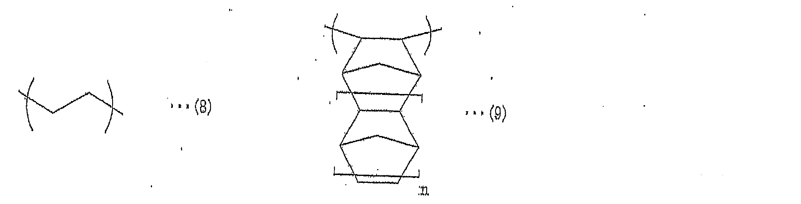
(化学式(9)中、nは0又は1~3の整数である。)
このようなシクロオレフィンコポリマーとして、APL 8008T、APL 8009T、及びAPL 6013T(全て三井化学株式会社製)などを使用できる。
このようなシクロオレフィンコポリマーとして、APL 8008T、APL 8009T、及びAPL 6013T(全て三井化学株式会社製)などを使用できる。
なお、光硬化性樹脂(例えば、UV硬化性樹脂)以外の樹脂を用いて接着層14を形成することが好ましい。これは、光硬化性樹脂が、接着層14の剥離又は除去の後に、基板11の微小な凹凸の周辺に残渣として残ってしまう場合があり得るからである。特に、特定の溶剤に溶解する接着剤が接着層14を構成する材料として好ましい。これは、基板11に物理的な力を加えることなく、接着層14を溶剤に溶解させることによって除去可能なためである。接着層14を除去するときに、強度が低下した基板11からでさえ、基板11を破損させたり、変形させたりせずに、容易に接着層14を除去できる。
上述した分離層、接着層を形成するための希釈溶剤としては、ヘキサン、ヘプタン、オクタン、ノナン、メチルオクタン、デカン、ウンデカン、ドデカン、トリデカン等の直鎖状の炭化水素、炭素数3から15の分岐状の炭化水素(例えば、)、p-メンタン、o-メンタン、m-メンタン、ジフェニルメンタン、1,4-テルピン、1,8-テルピン、ボルナン、ノルボルナン、ピナン、ツジャン、カラン、ロンギホレン、ゲラニオール、ネロール、リナロール、シトラール、シトロネロール、メントール、イソメントール、ネオメントール、α-テルピネオール、β-テルピネオール、γ-テルピネオール、テルピネン-1-オール、テルピネン-4-オール、ジヒドロターピニルアセテート、1,4-シネオール、1,8-シネオール、ボルネオール、カルボン、ヨノン、ツヨン、カンファー、d-リモネン、l-リモネン、ジペンテン等のテルペン系溶剤;γ-ブチロラクトン等のラクトン類;アセトン、メチルエチルケトン、シクロヘキサノン(CH)、メチル-n-ペンチルケトン、メチルイソペンチルケトン、2-ヘプタノン等のケトン類;エチレングリコール、ジエチレングリコール、プロピレングリコール、ジプロピレングリコール等の多価アルコール類;エチレングリコールモノアセテート、ジエチレングリコールモノアセテート、プロピレングリコールモノアセテート、又はジプロピレングリコールモノアセテート等のエステル結合を有する化合物、前記多価アルコール類又は前記エステル結合を有する化合物のモノメチルエーテル、モノエチルエーテル、モノプロピルエーテル、モノブチルエーテル等のモノアルキルエーテル又はモノフェニルエーテル等のエーテル結合を有する化合物等の多価アルコール類の誘導体(これらの中では、プロピレングリコールモノメチルエーテルアセテート(PGMEA)、プロピレングリコールモノメチルエーテル(PGME)が好ましい);ジオキサンのような環式エーテル類や、乳酸メチル、乳酸エチル(EL)、酢酸メチル、酢酸エチル、酢酸ブチル、メトキシブチルアセテート、ピルビン酸メチル、ピルビン酸エチル、メトキシプロピオン酸メチル、エトキシプロピオン酸エチル等のエステル類;アニソール、エチルベンジルエーテル、クレジルメチルエーテル、ジフェニルエーテル、ジベンジルエーテル、フェネトール、ブチルフェニルエーテル等の芳香族系有機溶剤等が挙げられる。
<エラストマー>
エラストマーは、主鎖の構成単位としてスチレン単位を含んでいることが好ましい。接着剤として用いるエラストマーは、当該スチレン単位の含有量が14重量%以上、50重量%以下の範囲であることが好ましい。さらに、エラストマーは、重量平均分子量が10,000以上、200,000以下の範囲であることが好ましい。
エラストマーは、主鎖の構成単位としてスチレン単位を含んでいることが好ましい。接着剤として用いるエラストマーは、当該スチレン単位の含有量が14重量%以上、50重量%以下の範囲であることが好ましい。さらに、エラストマーは、重量平均分子量が10,000以上、200,000以下の範囲であることが好ましい。
エラストマーとしては、例えば、ポリスチレン-ポリ(エチレン/プロピレン)ブロックコポリマー(SEP)、スチレン-イソプレン-スチレンブロックコポリマー(SIS)、スチレン-ブタジエン-スチレンブロックコポリマー(SBS)、スチレン-ブタジエン-ブチレン-スチレンブロックコポリマー(SBBS)、エチレン-プロピレンターポリマー(EPT)、これらの水添物、スチレン-エチレン-ブチレン-スチレンブロックコポリマー(SEBS)、スチレン-エチレン-プロピレン-スチレンブロックコポリマー(スチレン-イソプレン-スチレンブロックコポリマー)(SEPS)、及び、スチレン-エチレン-エチレン-プロピレン-スチレンブロックコポリマー(SEEPS)等が挙げられる。
<その他の成分>
接着材料には、本発明における本質的な特性を損なわない範囲において、混和性のある他の物質をさらに含んでいてもよい。例えば、接着剤の性能を改良するための付加的樹脂、可塑剤、接着補助剤、安定剤、着色剤、酸化防止剤及び界面活性剤等、慣用されている種々の添加剤をさらに用いることができる。
接着材料には、本発明における本質的な特性を損なわない範囲において、混和性のある他の物質をさらに含んでいてもよい。例えば、接着剤の性能を改良するための付加的樹脂、可塑剤、接着補助剤、安定剤、着色剤、酸化防止剤及び界面活性剤等、慣用されている種々の添加剤をさらに用いることができる。
〔積層体の分離方法〕
続いて、本実施形態に係る積層体の分離方法について説明する。
続いて、本実施形態に係る積層体の分離方法について説明する。
(照射工程)
本実施形態に係る積層体の分離方法においては、まず、図1中(1)に示すように、サポートプレート12を介して、パルス化されたレーザー光を分離層16に照射する(照射工程)。このとき、照射されたレーザー光は、光透過性を有するサポートプレート12を透過して、分離層16に到達する。分離層16は到達したレーザー光を吸収することによって、図1中(2)に示すように変質する。これにより、基板11とサポートプレート12との接着が弱まり、図1中(3)に示すように、基板11からサポートプレート12が容易に分離される。
本実施形態に係る積層体の分離方法においては、まず、図1中(1)に示すように、サポートプレート12を介して、パルス化されたレーザー光を分離層16に照射する(照射工程)。このとき、照射されたレーザー光は、光透過性を有するサポートプレート12を透過して、分離層16に到達する。分離層16は到達したレーザー光を吸収することによって、図1中(2)に示すように変質する。これにより、基板11とサポートプレート12との接着が弱まり、図1中(3)に示すように、基板11からサポートプレート12が容易に分離される。
積層体1からサポートプレート12を分離するために、サポートプレート12側からレーザー光を分離層16に照射したとき、分離層16からそのレーザー光が漏れることがある。
そのため、漏れた光が、基板11に到達してしまい、基板11自体又は基板11に形成されている保護されるべき電子回路等の電子素子が、漏れた光による悪影響を受けてしまうおそれがある。漏れた光による悪影響としては、基板11に実装されている電子回路の分解、基板11の損傷等が挙げられる。
この問題を回避するために、本発明者らは、分離層16に照射されるレーザー光によって、基板11及び基板11に形成された電子素子が受けるダメージについて鋭意検討を重ねた。その結果、分離層16のOD値として0.20以上、1.00以下を選択すればよいことを見出した。分離層16におけるこのようなOD値の選択は、レーザー光の照射によって、レーザー光の透過光が基板11にダメージを与えず、かつ分離層16を所望のように変質させることを可能にした。
特に、以下の条件において、基板11へのダメージを好適に防ぐことができる。言い換えれば、分離層16のOD値を、0.20以上、1.00以下としたとき、レーザー光の照射条件は、以下のように設定することが好ましい。
すなわち、レーザー光の平均出力値は、1.0W以上、5.0W以下の範囲であることが好ましく、3.0W以上、4.0W以下の範囲であることがより好ましい。また、レーザー光の繰り返し周波数は、20kHz以上、60kHz以下の範囲であることが好ましく、30kHz以上、50kHz以下の範囲であることがより好ましい。また、レーザー光の波長は、300nm以上、700nm以下であることが好ましく、450nm以上、650nm以下の範囲であることがより好ましい。このような条件によれば、分離層16に照射するパルス光のエネルギーを、基板11へのダメージを防ぎつつ、分離層16を変質させるための適切な条件にすることができる。
また、上記分離層16の分離工程に使用されるパルス光のビームスポット径は、100μm以上、250μm以下であることが好ましく、120μm以上、230μm以下であることがより好ましい。
また、パルス光の照射ピッチは、隣接するビームスポットが重ならず、かつ分離層16を変質させることが可能なピッチであればよいが、110μm以上、250μm以下であることが好ましく、160μm以上、220μm以下であることがより好ましい。
さらに、パルス光の照射速度は、分離層16を変質させることが可能な速度であればよいが、4000mm/s以上、10000mm/s以下であることが好ましく、5000mm/s以上、8000mm/s以下であることがより好ましい。
上記条件とすることで、レーザー光のビームスポットの重複が回避される。つまり、分離層16へ照射されるレーザー光のエネルギーの機械的側面からのばらつき(レーザー装置の設定によるばらつき)を制御できる。従って、OD値が規定された本実施形態に係る積層体に対して用いるレーザー光の照射条件として、好適に用いることができる。
さらに、分離層16に照射するパルス光のパルス幅は、20ナノ秒以上であることが好ましい。より好ましくは、40ナノ秒以上であり、さらに好ましくは、70ナノ秒以上である。分離層16に照射するパルス光のパルス幅の上限値は、200ナノ秒であることが好ましく、150ナノ秒であることがより好ましい。これにより、分離層16に吸収されずに漏れた光が、基板11及び基板11に形成された電子素子に及ぼす悪影響を、より抑えることができる。
積層体の分離方法においてパルス光を照射する照射装置としては、分離層16にパルス幅が20ナノ秒以上のパルス光を照射することができれば、特に限定されず、YAGレーザー、ルビーレーザー、ガラスレーザー、YVO4レーザー、LDレーザー、ファイバーレーザー等の固体レーザー発振器、色素レーザー等の液体レーザー発振器、CO2レーザー、エキシマレーザー、Arレーザー、He-Neレーザー等の気体レーザー発振器、半導体レーザー発振器、自由電子レーザー発振器等から適宜選択した発振器を使用できる。照射装置は、分離層16を構成している材料に応じて適宜選択することが可能であり、分離層16を構成する材料を変質させ得る光を照射するレーザーを選択すればよい。上記レーザー光の周波数は300nmから700nmであることが好ましい。レーザー光の周波数が当該範囲内であると、分離層に照射されたレーザー光が基板11及び基板11に形成された電子素子にダメージを与えることなく分離層16を変質させることが容易となる。
照射工程においては、パルス光を積層体1の全体に均一に照射することが好ましいが、基板11とサポートプレート12とを容易に分離できるように、分離層16を変質させることができれば、積層体1に部分的にパルス光を照射してよい。
(分離工程)
OD値が0.20以上、1.00以下である分離層16を用いた積層体1に、上記条件のレーザー光照射を行った場合、分離層16はレーザー照射を受けて変質するため、サポートプレート12は単に持ち上げるだけで、基板11から容易に分離する。
OD値が0.20以上、1.00以下である分離層16を用いた積層体1に、上記条件のレーザー光照射を行った場合、分離層16はレーザー照射を受けて変質するため、サポートプレート12は単に持ち上げるだけで、基板11から容易に分離する。
積層体の分離方法によれば、分離層16のOD値を0.20以上、1.00以下に調整することで、パルス発振されたレーザー光の適切な繰り返し周波数、及び平均出力を設定可能である。従って適切に設定されたレーザー光照射するので、分離層16において吸収されずに漏れた光が、基板11に到達したとしても、基板11及び基板11に形成された電子素子にダメージを与えることがない。また、分離層16を変質させるのに必要なエネルギー強度の光を分離層16に照射できるので、基板11とサポートプレート12とを容易に分離できる。
すなわち、積層体の分離方法によれば、製造プロセス中には基板11とサポートプレート12との強固な接着を実現しつつ、製造プロセス後には光照射によって容易に基板11とサポートプレート12とを分離可能であるとともに、光による基板11への悪影響を防止できるという効果を奏する。
〔分離層の評価方法〕
また、他の観点から見れば、本発明は、分離層のOD値を測定する測定工程を包含する分離層の評価方法を提供する。すなわち、上述のように、分離層のOD値が所定の範囲内であれば、基板表面へのダメージを防止できる。よって、分離層のOD値を測定することによって、当該分離層が、基板表面へダメージを与える光を透過させないか否かを評価できる。
また、他の観点から見れば、本発明は、分離層のOD値を測定する測定工程を包含する分離層の評価方法を提供する。すなわち、上述のように、分離層のOD値が所定の範囲内であれば、基板表面へのダメージを防止できる。よって、分離層のOD値を測定することによって、当該分離層が、基板表面へダメージを与える光を透過させないか否かを評価できる。
一実施形態において、分離層の評価方法では、測定工程において測定した分離層のOD値が0.20以上である場合、当該分離層が、基板表面へダメージを与えるような光を透過させないと決定できる。さらに好ましくは、測定工程において測定した分離層のOD値が0.20以上、1.00以下である場合、当該分離層が、基板表面へダメージを与える光を透過させないと決定できる。このようにして、照射工程において、基板表面が受けるダメージに起因する不良品の製造を回避できる。なお、このときの照射工程におけるレーザー光の平均出力値は、1.0W以上、5.0W以下の範囲であることが好ましく、3.0W以上、4.0W以下の範囲であることがより好ましい。また、レーザー光の繰り返し周波数は、20kHz以上、60kHz以下の範囲であることが好ましく、30kHz以上、50kHz以下の範囲であることがより好ましい。また、レーザー光の波長は、300nm以上、700nm以下であることが好ましく、450nm以上、650nm以下の範囲であることがより好ましい。また、パルス光のビームスポット径は、100μm以上、250μm以下であることが好ましく、120μm以上、230μm以下であることがより好ましい。また、パルス光の照射ピッチは、隣接するビームスポットが重ならず、かつ分離層16を変質させることが可能なピッチであればよいが、110μm以上、250μm以下であることが好ましく、160μm以上、220μm以下であることがより好ましい。さらに、パルス光の照射速度は、分離層16を変質させることが可能な速度であればよいが、4000mm/s以上、10000mm/s以下であることが好ましく、5000mm/s以上、8000mm/s以下であることがより好ましい。さらに、分離層16に照射するパルス光のパルス幅は、20ナノ秒以上であることが好ましい。より好ましくは、40ナノ秒以上であり、さらに好ましくは、70ナノ秒以上である。分離層16に照射するパルス光のパルス幅の上限値は、200ナノ秒であることが好ましく、150ナノ秒であることがより好ましい。
以下に実施例を示し、本発明の実施形態のさらなる詳細を説明する。もちろん、本発明は、以下の実施例に限定されず、細部には種々の態様を採用可能であることはいうまでもない。さらに、本発明は、上述した実施形態に限定されるものではなく、請求の範囲に示した範囲で種々の変更が可能であり、各実施形態にそれぞれ開示された技術的手段を適宜組み合わせて得られる実施形態についても本発明の技術的範囲に含まれる。また、本明細書中に記載された文献の全てが参考として援用される。
(出力と剥離可能範囲の評価)
12インチベアガラス(サポートプレート)に流量400sccm、圧力700mTorr、高周波電力2500W及び成膜温度240℃の条件下において、反応ガスとしてC4F8を使用したプラズマCVD法により、フルオロカーボン膜(0.5μm)を形成した(分離層形成工程)。
12インチベアガラス(サポートプレート)に流量400sccm、圧力700mTorr、高周波電力2500W及び成膜温度240℃の条件下において、反応ガスとしてC4F8を使用したプラズマCVD法により、フルオロカーボン膜(0.5μm)を形成した(分離層形成工程)。
同じく分離層形成工程として、積層体を製造する平行平板電極を備えた反応室の条件は、高周波電源の出力電力1.0kW、圧力67Pa、及び成膜温度220℃に調整した。該反応室において、まず、流量200sccmに調整したイソプレンを反応ガスとして供給して、プラズマCVD法によるプラズマ処理を行なった。その後、プラズマ処理を中断せずに、流量100sccmに調整したイソプレンおよび流量100sccmに調整した6フッ化硫黄(SF6)を、1:1の割合において含有する反応ガスを供給して、プラズマCVD法によるプラズマ処理を行なった。これにより、イソプレンと6フッ化硫黄(SF6)から形成される分離層(膜厚0.5μm)を、12インチベアガラスに形成した。当該分離層を便宜的に「イソプレン膜」と称する。
また、12インチシリコンウエハ(基板)には接着剤組成物(TZNR-A3007、東京応化工業株式会社製)を塗布し、100℃、160℃、200℃で各3分焼いて接着剤層(膜厚50μm)を形成した(接着層形成工程)。そして、真空下の220℃、4000Kgの条件で3分間、フルオロカーボン膜を形成したガラス支持体と貼り合せを行い積層体とした(積層工程)。
そして、レーザー光の波長を532nm、レーザー光の直径を180μmとして、レーザパルスにおける被照射領域同士の中心間距離を180μm、走査速度を7200mm/sとして、レーザー光の平均出力及び繰り返し周波数を変更した条件でレーザー光照射を行い、分離層を剥離し得るか否かを判定した。
評価結果を表1に示す。なお、表1では、レーザー光を照射した後、サポートプレートが剥離できた条件を「○」、剥離できなかった条件を「×」で示す。
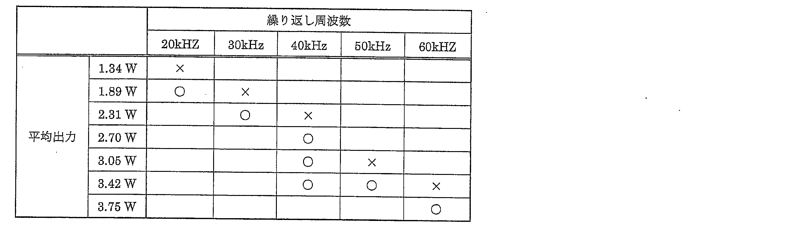
以上の結果を踏まえ、平均出力3.42W、繰り返し周波数40kHzを標準条件として、以下の検討を行った。
(OD値とSn-Ag装着基板へのダメージとの関係の検討)
続いて、CVD法による分離層の成膜時間の異なるサポートプレートを作成し、分離層のOD値を測定した後、レーザー光を発振するレーザー照射装置を用いて、レーザー光が基板に及ぼす影響を調べた。
続いて、CVD法による分離層の成膜時間の異なるサポートプレートを作成し、分離層のOD値を測定した後、レーザー光を発振するレーザー照射装置を用いて、レーザー光が基板に及ぼす影響を調べた。
12インチベアガラス(サポートプレート)に流量400sccm、圧力700mTorr、高周波電力2500W及び成膜温度240℃の条件下において、反応ガスとしてC4F8を使用したプラズマCVD法により、フルオロカーボン膜を形成した(分離層形成工程)。このとき、分離層の膜厚の目標をそれぞれ2000Å(0.2μm)、4500Å(0.45μm)、7000Å(0.7μm)として、成膜時間を3条件で変化させた。このとき、1つの条件につき、2点ずつ分離層を作成した(膜厚2000Åの分離層について(1)および(2)、膜厚4500Åの分離層について(3)および(4)、膜厚7000Åの分離層について(5)および(6))。
次に、X-Rite310(OD値測定機、エックスライト社製)を用いて上記各分離層の中心位置から一定距離ごとにOD値を測定した。結果を表2および図4(a)に示す。なお、OD値は、表2、図4(a)および(b)に示すとおり、サポートプレート上の分離層における中心からの距離が異なる各位置において測定した。分離層の中心から120mmまでの距離では6mmのピッチで、中心から120mm以上150mmまでは3mmのピッチで測定した。
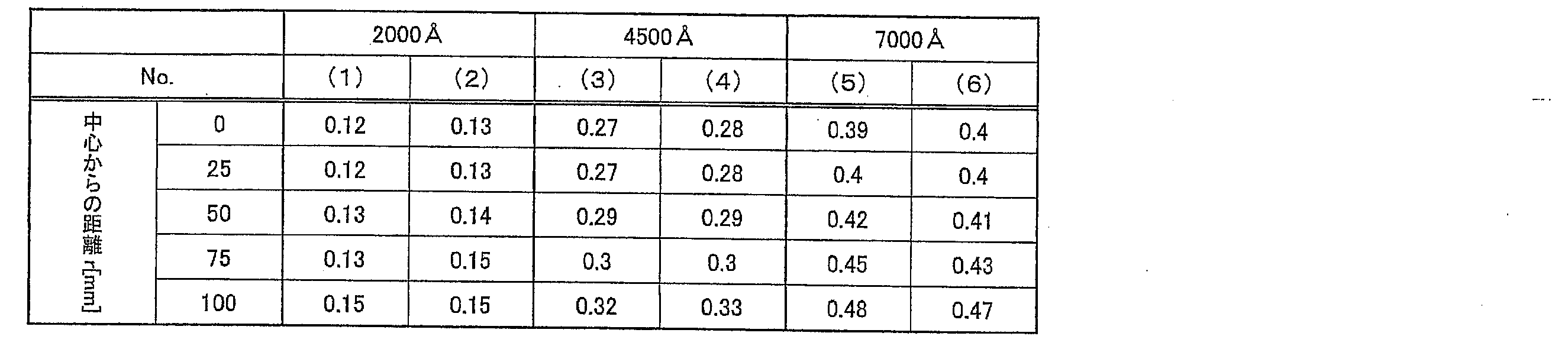
また、フルオロカーボン膜またはイソプレン膜を、分離層として形成して、同様の条件下において、OD値を測定した。結果は表3および図5に示す通りである。
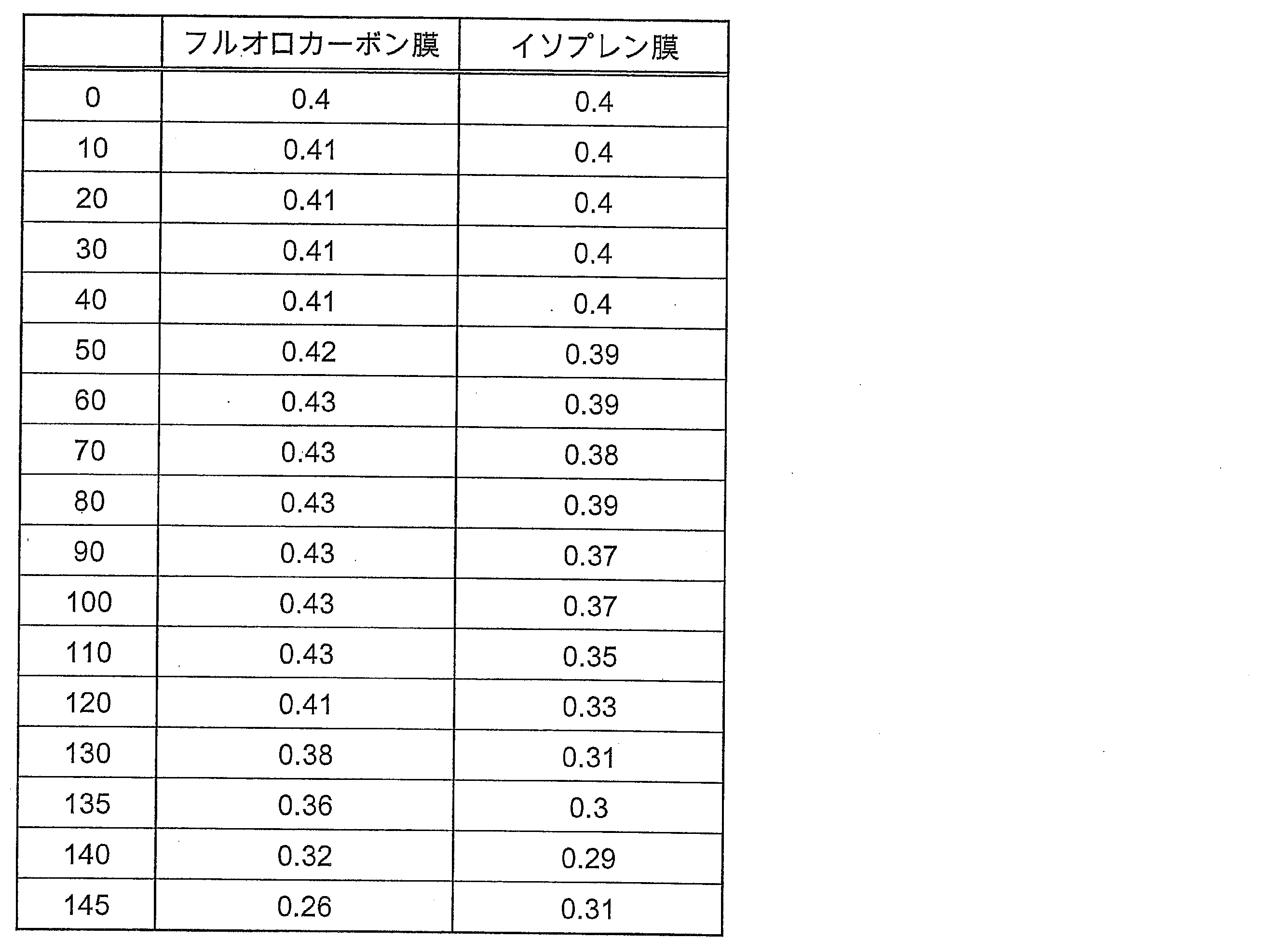
また、Sn-Ag板(スズ-銀板、0.3~0.4μm)を装着した12インチシリコンウエハ(基板)のSn-Ag板上に接着剤組成物(TZNR-A3007、東京応化工業株式会社製)を塗布し、100℃、160℃、200℃において各3分間焼いて接着剤層(膜厚50μm)を形成した(接着層形成工程)。なお、上記Sn-Ag板を、ウエハ基板に実装される素子、電気回路等の代わりとして使用した。そして、真空下の220℃、4000Kgの条件で3分間、フルオロカーボン膜を形成したガラス支持体と貼り合せを行い積層体とした(積層工程)。
そして、レーザー光の波長を532nm、レーザー光の直径を180μmとして、レーザパルスにおける被照射領域同士の中心間距離を180μm、走査速度を7200mm/sとして、レーザー光の平均出力3.42W、繰り返し周波数40kHzでレーザー光照射を行った。
上記条件でレーザー光を照射した後、Sn-Ag板が受けるダメージについて、顕微鏡にて目視で確認した。Sn-Ag板上に、レーザー光のビームスポットが形成された場合には、ダメージ有とし、形成されていない場合には、ダメージ無とした。
確認の結果、全面的にOD値が0.30より低かったTarget:2000Aでは、(1)及び(2)共にいずれの位置においてもSn-Ag板上にダメージが認められた。Target:4500Aでは、(3)及び(4)共にOD値が0.29であった位置では、Sn-Ag板上にわずかなダメージが認められたが、OD値が0.30以上1.00以下の位置ではSn-Ag板上にダメージは認められなかった。全面的にOD値が0.30以上1.00以下であるTarget:7000Aでは、(5)及び(6)共にいずれの位置においてもSn-Ag板上にダメージは認められなかった。
(OD値と各種基板へのダメージとの関係の検討)
続いて、ウエハ基板に実装される素子、電気回路等の代わりに、各種の材料を装着した12インチシリコンウエハ(基板)を用いたそれぞれ積層体を作成し、CVD法による分離層の成膜時間を調整することで、異なるOD値を示す分離層を形成するサポートプレートを作成し、それぞれの条件を組み合わせた積層体を作成し、レーザー光を照射することで、レーザー光が各材料に及ぼす効果について、Sn-Ag板の場合と比較検討を行なった。
続いて、ウエハ基板に実装される素子、電気回路等の代わりに、各種の材料を装着した12インチシリコンウエハ(基板)を用いたそれぞれ積層体を作成し、CVD法による分離層の成膜時間を調整することで、異なるOD値を示す分離層を形成するサポートプレートを作成し、それぞれの条件を組み合わせた積層体を作成し、レーザー光を照射することで、レーザー光が各材料に及ぼす効果について、Sn-Ag板の場合と比較検討を行なった。
素子、電気回路の代わりに用いた材料は、Cu(1μm)、SiO2(1μm)、Al(0.2μm)、およびポリイミド(0.1μm)であり、これらを12インチシリコンウエハ(基板)に装着したものを評価に用いた。また、ベアシリコンウエハについても同様の評価を行い、Sn-Ag板の場合と比較した。
12インチベアガラス(サポートプレート)に流量400sccm、圧力700mTorr、高周波電力2500W及び成膜温度240℃の条件下において、反応ガスとしてC4F8を使用したプラズマCVD法により、フルオロカーボン膜を形成した(分離層形成工程)。この際、分離層の膜厚の目標をそれぞれ2000Å(0.2μm)、4500Å(0.45μm)、7000Å(0.7μm)として、成膜時間を3条件で変化させた。また、比較のため、分離層を形成しないサポートプレート(下記表3における「直接」)についても準備した。
次に、X-Rite310(OD値測定機、エックスライト社製)を用いて上記各分離層の中心位置から一定距離のOD値を測定した。分離層の膜厚目標が2000Åのものは、OD値はおよそ0.15、膜厚目標が4500Åのものは、OD値がおよそ0.30、膜厚目標が7000Åのものは、OD値がおよそ0.45となった。
次に、各種の材料を装着した(又は装着していない)12インチシリコンウエハ(基板)上に接着剤組成物(TZNR-A3007、東京応化工業株式会社製)を塗布し、100℃、160℃、200℃において各3分間焼いて接着剤層(膜厚50μm)を形成した(接着層形成工程)。次に、各種基板を、それぞれ、真空下の220℃、4000Kgの条件で3分間、各種ガラス支持体(フルオロカーボン膜を有している)と貼り合せを行い積層体とした(積層工程)。
そして、レーザー光の波長を532nm、レーザー光の直径を180μmとし、レーザパルスにおける被照射領域同士の中心間距離を180μm、走査速度を7300mm/sとし、レーザー光の平均出力3.42W、繰り返し周波数40kHzでレーザー光照射を行った。
上記条件でレーザー光を照射した後、各種基板が受けたダメージについて、顕微鏡にて目視で確認した。基板上に、レーザー光のビームスポットが形成された場合には、ダメージ有とし、形成されていない場合には、ダメージ無とした。確認の結果を表4に示す。

表4に示すように、基板に装着された材料の種類によって結果に違いが生じた。すなわち、レーザー光による基板上の素子、電気回路等へのダメージを回避するために必要なOD値は、基板によって異なっていた。ただし、基板に装着された材料の種類に合わせて適切なOD値を選択することによって、いずれの場合においても、レーザー光による基板上の素子、電気回路等へのダメージを回避し得ることが示された。
また、イソプレン膜の分離層としての作用を、フルオロカーボン膜の評価と同様の条件において評価した。その結果、イソプレン膜についても、フルオロカーボン膜と同様の結果が得られた。
本発明は、例えば、微細化された半導体装置の製造工程において好適に利用できる。
1 積層体
11 基板
12 サポートプレート(支持体)
14 接着層
16 分離層
16a 第1の分離層
16b 第2の分離層
20 積層体
11 基板
12 サポートプレート(支持体)
14 接着層
16 分離層
16a 第1の分離層
16b 第2の分離層
20 積層体
Claims (7)
- 基板と、接着層と、光を吸収することにより変質する分離層と、光透過性の支持体とがこの順番に積層された積層体であって、
該分離層のOD値が、0.20以上、1.00以下であることを特徴とする積層体。 - 上記分離層は、炭化水素ガスおよびフッ化炭素ガスの少なくとも何れかを含有する反応ガスを用いたプラズマCVD法により形成されたものであることを特徴とする請求項1に記載の積層体。
- 上記分離層の厚さが、0.05μm以上、100μm以下であることを特徴とする請求項1又は2に記載の積層体。
- 基板と、接着層と、OD値が0.20以上、1.00以下であり、光を吸収することにより変質する分離層と、光透過性の支持体とがこの順番に積層された積層体を分離する積層体の分離方法であって、
該支持体を介して、該分離層に上記OD値から設定される繰り返し周波数および平均出力値を有するレーザー光を照射する照射工程と、
該照射工程の後、該基板と該支持体とを分離する分離工程とを包含することを特徴とする積層体の分離方法。 - 上記レーザー光の波長が、300nm以上、700nm以下であることを特徴とする請求項4に記載の積層体の分離方法。
- 基板と、接着層と、光を吸収することにより変質する分離層と、光透過性の支持体とがこの順番に積層された積層体の分離層を評価する分離層の評価方法であって、
該分離層のOD値を測定する測定工程を包含することを特徴とする分離層の評価方法。 - 上記測定工程にて測定した上記OD値が0.20以上であるか否かによって上記分離層を評価する評価工程を包含することを特徴とする請求項6に記載の分離層の評価方法。
Priority Applications (1)
| Application Number | Priority Date | Filing Date | Title |
|---|---|---|---|
| JP2014538496A JP6261508B2 (ja) | 2012-09-28 | 2013-09-24 | 積層体、積層体の分離方法、および分離層の評価方法 |
Applications Claiming Priority (2)
| Application Number | Priority Date | Filing Date | Title |
|---|---|---|---|
| JP2012218718 | 2012-09-28 | ||
| JP2012-218718 | 2012-09-28 |
Publications (1)
| Publication Number | Publication Date |
|---|---|
| WO2014050820A1 true WO2014050820A1 (ja) | 2014-04-03 |
Family
ID=50388219
Family Applications (1)
| Application Number | Title | Priority Date | Filing Date |
|---|---|---|---|
| PCT/JP2013/075722 Ceased WO2014050820A1 (ja) | 2012-09-28 | 2013-09-24 | 積層体、積層体の分離方法、および分離層の評価方法 |
Country Status (3)
| Country | Link |
|---|---|
| JP (1) | JP6261508B2 (ja) |
| TW (1) | TWI573693B (ja) |
| WO (1) | WO2014050820A1 (ja) |
Cited By (5)
| Publication number | Priority date | Publication date | Assignee | Title |
|---|---|---|---|---|
| JP2015217566A (ja) * | 2014-05-15 | 2015-12-07 | 東京応化工業株式会社 | 積層体の製造方法および積層体 |
| JP2016092079A (ja) * | 2014-10-30 | 2016-05-23 | 東京応化工業株式会社 | 支持体分離方法 |
| WO2020080276A1 (ja) * | 2018-10-16 | 2020-04-23 | 富士フイルム株式会社 | レーザ剥離用の積層体、組成物およびキット |
| JPWO2022210154A1 (ja) * | 2021-04-01 | 2022-10-06 | ||
| JP2024084824A (ja) * | 2015-11-02 | 2024-06-25 | エーファウ・グループ・エー・タルナー・ゲーエムベーハー | 基板を結合および剥離させる方法 |
Families Citing this family (2)
| Publication number | Priority date | Publication date | Assignee | Title |
|---|---|---|---|---|
| JP6437805B2 (ja) * | 2014-12-03 | 2018-12-12 | 東京応化工業株式会社 | 積層体の製造方法、封止基板積層体の製造方法及び積層体 |
| JP6486735B2 (ja) * | 2015-03-17 | 2019-03-20 | 東芝メモリ株式会社 | 半導体製造方法および半導体製造装置 |
Citations (4)
| Publication number | Priority date | Publication date | Assignee | Title |
|---|---|---|---|---|
| JP2007015377A (ja) * | 2005-06-07 | 2007-01-25 | Fujifilm Holdings Corp | 機能性膜含有構造体、及び、機能性膜の製造方法 |
| JP2011076767A (ja) * | 2009-09-29 | 2011-04-14 | Dainippon Printing Co Ltd | 積層体、準備用支持体、積層体の製造方法、及びデバイスの製造方法 |
| WO2012056969A1 (ja) * | 2010-10-29 | 2012-05-03 | 東京応化工業株式会社 | 積層体、およびその積層体の分離方法 |
| JP2012124467A (ja) * | 2010-11-15 | 2012-06-28 | Tokyo Ohka Kogyo Co Ltd | 積層体、および分離方法 |
Family Cites Families (1)
| Publication number | Priority date | Publication date | Assignee | Title |
|---|---|---|---|---|
| JP5756334B2 (ja) * | 2010-10-29 | 2015-07-29 | 東京応化工業株式会社 | 積層体、およびその積層体の分離方法 |
-
2013
- 2013-09-24 JP JP2014538496A patent/JP6261508B2/ja active Active
- 2013-09-24 WO PCT/JP2013/075722 patent/WO2014050820A1/ja not_active Ceased
- 2013-09-26 TW TW102134822A patent/TWI573693B/zh active
Patent Citations (4)
| Publication number | Priority date | Publication date | Assignee | Title |
|---|---|---|---|---|
| JP2007015377A (ja) * | 2005-06-07 | 2007-01-25 | Fujifilm Holdings Corp | 機能性膜含有構造体、及び、機能性膜の製造方法 |
| JP2011076767A (ja) * | 2009-09-29 | 2011-04-14 | Dainippon Printing Co Ltd | 積層体、準備用支持体、積層体の製造方法、及びデバイスの製造方法 |
| WO2012056969A1 (ja) * | 2010-10-29 | 2012-05-03 | 東京応化工業株式会社 | 積層体、およびその積層体の分離方法 |
| JP2012124467A (ja) * | 2010-11-15 | 2012-06-28 | Tokyo Ohka Kogyo Co Ltd | 積層体、および分離方法 |
Cited By (9)
| Publication number | Priority date | Publication date | Assignee | Title |
|---|---|---|---|---|
| JP2015217566A (ja) * | 2014-05-15 | 2015-12-07 | 東京応化工業株式会社 | 積層体の製造方法および積層体 |
| JP2016092079A (ja) * | 2014-10-30 | 2016-05-23 | 東京応化工業株式会社 | 支持体分離方法 |
| JP2024084824A (ja) * | 2015-11-02 | 2024-06-25 | エーファウ・グループ・エー・タルナー・ゲーエムベーハー | 基板を結合および剥離させる方法 |
| JP7778837B2 (ja) | 2015-11-02 | 2025-12-02 | エーファウ・グループ・エー・タルナー・ゲーエムベーハー | 基板を結合および剥離させる方法 |
| WO2020080276A1 (ja) * | 2018-10-16 | 2020-04-23 | 富士フイルム株式会社 | レーザ剥離用の積層体、組成物およびキット |
| JPWO2022210154A1 (ja) * | 2021-04-01 | 2022-10-06 | ||
| WO2022210154A1 (ja) * | 2021-04-01 | 2022-10-06 | 東レ株式会社 | 積層体および半導体装置の製造方法 |
| JP7790341B2 (ja) | 2021-04-01 | 2025-12-23 | 東レ株式会社 | 積層体および半導体装置の製造方法 |
| US12534399B2 (en) | 2021-04-01 | 2026-01-27 | Toray Industries, Inc. | Laminate and manufacturing method of semiconductor device |
Also Published As
| Publication number | Publication date |
|---|---|
| TW201420355A (zh) | 2014-06-01 |
| JPWO2014050820A1 (ja) | 2016-08-22 |
| JP6261508B2 (ja) | 2018-01-17 |
| TWI573693B (zh) | 2017-03-11 |
Similar Documents
| Publication | Publication Date | Title |
|---|---|---|
| JP5977532B2 (ja) | 支持体分離方法及び支持体分離装置 | |
| JP6088230B2 (ja) | 積層体の形成方法 | |
| US9627235B2 (en) | Supporting member separation method | |
| JP6261508B2 (ja) | 積層体、積層体の分離方法、および分離層の評価方法 | |
| JP5864926B2 (ja) | 積層体、分離方法、及び製造方法 | |
| WO2013172110A1 (ja) | 支持体分離方法および支持体分離装置 | |
| TWI720004B (zh) | 支撐體分離方法 | |
| US10607876B2 (en) | Method for processing mold material and method for manufacturing structural body | |
| WO2017026279A1 (ja) | 支持体分離装置及び支持体分離方法 | |
| JP2013172033A (ja) | 分離方法及び積層構造体 | |
| JP6180239B2 (ja) | 積層体の製造方法及び積層体 | |
| JP6030358B2 (ja) | 積層体 | |
| TWI636884B (zh) | 處理方法 | |
| JP6214182B2 (ja) | 基板の処理方法 | |
| JP6006569B2 (ja) | 積層体及び積層体の製造方法 | |
| JP6298393B2 (ja) | 支持体分離方法 | |
| JP6691816B2 (ja) | 封止体の製造方法 | |
| JP6055354B2 (ja) | 基板の処理方法 | |
| JP6077810B2 (ja) | プラズマ処理装置、プラズマ処理方法および積層体の製造方法 | |
| JP6101031B2 (ja) | プラズマ処理装置および積層体の製造方法 | |
| JP2014070257A (ja) | 積層体の製造方法、および分離層形成装置 | |
| JP2015046514A (ja) | 積層体の製造方法及び積層体 | |
| JP2014069494A (ja) | 積層体の製造方法および積層体 |
Legal Events
| Date | Code | Title | Description |
|---|---|---|---|
| 121 | Ep: the epo has been informed by wipo that ep was designated in this application |
Ref document number: 13840218 Country of ref document: EP Kind code of ref document: A1 |
|
| ENP | Entry into the national phase |
Ref document number: 2014538496 Country of ref document: JP Kind code of ref document: A |
|
| NENP | Non-entry into the national phase |
Ref country code: DE |
|
| 122 | Ep: pct application non-entry in european phase |
Ref document number: 13840218 Country of ref document: EP Kind code of ref document: A1 |