WO2014050464A1 - 基板処理装置、基板処理方法、及び半導体装置の製造方法 - Google Patents
基板処理装置、基板処理方法、及び半導体装置の製造方法 Download PDFInfo
- Publication number
- WO2014050464A1 WO2014050464A1 PCT/JP2013/073742 JP2013073742W WO2014050464A1 WO 2014050464 A1 WO2014050464 A1 WO 2014050464A1 JP 2013073742 W JP2013073742 W JP 2013073742W WO 2014050464 A1 WO2014050464 A1 WO 2014050464A1
- Authority
- WO
- WIPO (PCT)
- Prior art keywords
- substrate
- transfer chamber
- chamber
- processing
- transfer
- Prior art date
- Legal status (The legal status is an assumption and is not a legal conclusion. Google has not performed a legal analysis and makes no representation as to the accuracy of the status listed.)
- Ceased
Links
Images

Classifications
-
- H—ELECTRICITY
- H10—SEMICONDUCTOR DEVICES; ELECTRIC SOLID-STATE DEVICES NOT OTHERWISE PROVIDED FOR
- H10P—GENERIC PROCESSES OR APPARATUS FOR THE MANUFACTURE OR TREATMENT OF DEVICES COVERED BY CLASS H10
- H10P72/00—Handling or holding of wafers, substrates or devices during manufacture or treatment thereof
- H10P72/04—Apparatus for manufacture or treatment
- H10P72/0451—Apparatus for manufacturing or treating in a plurality of work-stations
- H10P72/0464—Apparatus for manufacturing or treating in a plurality of work-stations characterised by the construction of the transfer chamber
-
- C—CHEMISTRY; METALLURGY
- C23—COATING METALLIC MATERIAL; COATING MATERIAL WITH METALLIC MATERIAL; CHEMICAL SURFACE TREATMENT; DIFFUSION TREATMENT OF METALLIC MATERIAL; COATING BY VACUUM EVAPORATION, BY SPUTTERING, BY ION IMPLANTATION OR BY CHEMICAL VAPOUR DEPOSITION, IN GENERAL; INHIBITING CORROSION OF METALLIC MATERIAL OR INCRUSTATION IN GENERAL
- C23C—COATING METALLIC MATERIAL; COATING MATERIAL WITH METALLIC MATERIAL; SURFACE TREATMENT OF METALLIC MATERIAL BY DIFFUSION INTO THE SURFACE, BY CHEMICAL CONVERSION OR SUBSTITUTION; COATING BY VACUUM EVAPORATION, BY SPUTTERING, BY ION IMPLANTATION OR BY CHEMICAL VAPOUR DEPOSITION, IN GENERAL
- C23C16/00—Chemical coating by decomposition of gaseous compounds, without leaving reaction products of surface material in the coating, i.e. chemical vapour deposition [CVD] processes
- C23C16/44—Chemical coating by decomposition of gaseous compounds, without leaving reaction products of surface material in the coating, i.e. chemical vapour deposition [CVD] processes characterised by the method of coating
- C23C16/54—Apparatus specially adapted for continuous coating
-
- H—ELECTRICITY
- H10—SEMICONDUCTOR DEVICES; ELECTRIC SOLID-STATE DEVICES NOT OTHERWISE PROVIDED FOR
- H10P—GENERIC PROCESSES OR APPARATUS FOR THE MANUFACTURE OR TREATMENT OF DEVICES COVERED BY CLASS H10
- H10P72/00—Handling or holding of wafers, substrates or devices during manufacture or treatment thereof
- H10P72/10—Handling or holding of wafers, substrates or devices during manufacture or treatment thereof using carriers specially adapted therefor, e.g. front opening unified pods [FOUP]
- H10P72/19—Handling or holding of wafers, substrates or devices during manufacture or treatment thereof using carriers specially adapted therefor, e.g. front opening unified pods [FOUP] closed carriers
- H10P72/1916—Handling or holding of wafers, substrates or devices during manufacture or treatment thereof using carriers specially adapted therefor, e.g. front opening unified pods [FOUP] closed carriers characterised by sealing arrangements
-
- H—ELECTRICITY
- H10—SEMICONDUCTOR DEVICES; ELECTRIC SOLID-STATE DEVICES NOT OTHERWISE PROVIDED FOR
- H10P—GENERIC PROCESSES OR APPARATUS FOR THE MANUFACTURE OR TREATMENT OF DEVICES COVERED BY CLASS H10
- H10P72/00—Handling or holding of wafers, substrates or devices during manufacture or treatment thereof
- H10P72/10—Handling or holding of wafers, substrates or devices during manufacture or treatment thereof using carriers specially adapted therefor, e.g. front opening unified pods [FOUP]
- H10P72/19—Handling or holding of wafers, substrates or devices during manufacture or treatment thereof using carriers specially adapted therefor, e.g. front opening unified pods [FOUP] closed carriers
- H10P72/1924—Handling or holding of wafers, substrates or devices during manufacture or treatment thereof using carriers specially adapted therefor, e.g. front opening unified pods [FOUP] closed carriers characterised by atmosphere control
-
- H—ELECTRICITY
- H10—SEMICONDUCTOR DEVICES; ELECTRIC SOLID-STATE DEVICES NOT OTHERWISE PROVIDED FOR
- H10P—GENERIC PROCESSES OR APPARATUS FOR THE MANUFACTURE OR TREATMENT OF DEVICES COVERED BY CLASS H10
- H10P72/00—Handling or holding of wafers, substrates or devices during manufacture or treatment thereof
- H10P72/30—Handling or holding of wafers, substrates or devices during manufacture or treatment thereof for conveying, e.g. between different workstations
- H10P72/33—Handling or holding of wafers, substrates or devices during manufacture or treatment thereof for conveying, e.g. between different workstations into and out of processing chamber
- H10P72/3312—Vertical transfer of a batch of workpieces
-
- H—ELECTRICITY
- H10—SEMICONDUCTOR DEVICES; ELECTRIC SOLID-STATE DEVICES NOT OTHERWISE PROVIDED FOR
- H10P—GENERIC PROCESSES OR APPARATUS FOR THE MANUFACTURE OR TREATMENT OF DEVICES COVERED BY CLASS H10
- H10P95/00—Generic processes or apparatus for manufacture or treatments not covered by the other groups of this subclass
- H10P95/90—Thermal treatments, e.g. annealing or sintering
Definitions
- a processing chamber for processing a substrate and a transfer chamber for transferring the substrate to the processing chamber are provided, and the transfer chamber has a plurality of walls forming a casing of the transfer chamber.
- Substrate processing using a substrate processing apparatus including a body, a joint where the plurality of wall bodies are joined, an isolation space forming member that covers the joint so as to form an isolation space isolated from the transport chamber There is provided a substrate processing method comprising: a step of carrying a substrate from the transfer chamber into the processing chamber; a step of exhausting the isolation space; a step of processing a substrate carried into the processing chamber; Is done.
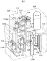
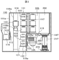
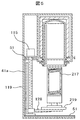
- a processing furnace 202 is provided above the boat 217.
- the processing furnace 202 includes a substrate processing chamber (not shown) inside, and a heater (not shown) that heats the substrate processing chamber around the substrate processing chamber.
- the lower end of the processing furnace 202 is opened and closed by a furnace port cap 147.
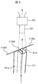
- the atmosphere in the isolated space formed by the hat rib 31, the wall body 119b, and the wall body 119c is sucked through a duct (ventilating pipe) 32 by a suction unit 33 including a blower (fan), a vacuum pump, or the like. Then, it is discharged out of the substrate processing apparatus 100.
- the duct 32 may be connected to the aforementioned transfer chamber exhaust part of the transfer chamber 124.
- the transfer chamber exhaust section is located downstream of the transfer chamber exhaust duct, the transfer chamber exhaust duct opening / closing valve provided in the transfer chamber exhaust duct, and the transfer chamber exhaust duct opening / closing valve. It is comprised by the transfer chamber suction part which consists of a provided vacuum pump.
- the soot duct 32 may be connected to the transfer chamber exhaust section at the subsequent stage of the suction section 33, or may be connected to the transfer chamber exhaust section without providing the suction section 33.
- a duct opening / closing valve (not shown) that controls the exhaust in the isolation space by opening and closing the duct 32 may be installed in the duct 32.
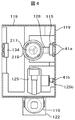
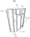
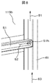
- the frame reinforcing column 51 is appropriately provided with a suction hole 41h shown in FIG. 7 so as to eliminate the stagnation of the atmosphere. Further, a duct 32 and a suction part 33 as shown in FIG. 3 are connected to the end of the mounting column 41 in the direction in which the atmosphere 81 flows.
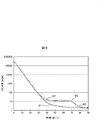
- FIG. 9 is a diagram for explaining the effect according to the second embodiment.
- the vertical axis represents oxygen concentration, and the horizontal axis represents time.
- 91 shows the time transition of the oxygen concentration in the transfer chamber 124 according to the second embodiment.
- Reference numeral 92 denotes a time transition of the oxygen concentration in the transfer chamber 124 according to the conventional structure.
- Reference numeral 94 denotes a time transition of the oxygen concentration when the atmospheric suction in the column according to the second example is started at the time 93 in the middle of 92.
- the atmosphere in the transfer chamber 124 is eliminated by exhausting the atmosphere in the column constituting the sub-housing 119, and the oxygen in the transfer chamber 124 is removed.
- the concentration can be reduced in a short time. ⁇ ⁇ ⁇
- the atmosphere in the pillar may be exhausted by connecting to the transfer chamber exhaust portion of the transfer chamber 124 and exhausting it.
- the transfer chamber includes a hollow structure reinforcing column that reinforces the casing of the transfer chamber, and is configured to exhaust the hollow portion of the rod reinforcing column.
- the casing reinforcing column and the hollow portion of the mounting column are connected, and the casing reinforcing column and the hollow portion of the mounting column are communicated with each other.
- the side surface of the isolation space forming member, the casing reinforcing column, and the mounting column is provided with at least one suction hole.
- a processing chamber for processing a substrate and a transfer chamber used for transferring the substrate to the substrate processing chamber are provided, and the transfer chamber is a transfer chamber.
- a method of manufacturing a semiconductor device using a substrate processing apparatus comprising: a step of loading a substrate from the transfer chamber into the processing chamber; a step of exhausting the isolation space; and a processing of the substrate transferred into the processing chamber.
- a process and a method for manufacturing a semiconductor device including a ridge are provided.
- a transport chamber for transporting the substrate to a processing chamber for processing a sputter substrate, a junction for joining a plurality of wall bodies, and isolation from the transport chamber Evacuating the isolation space forming portion of the transfer chamber having an isolation space forming portion that covers the joining portion so as to form a separated isolation space, carrying the substrate into the processing chamber, and A step of processing a substrate and a method of manufacturing a semiconductor device having a ridge are provided.
Landscapes
- Chemical & Material Sciences (AREA)
- General Chemical & Material Sciences (AREA)
- Chemical Kinetics & Catalysis (AREA)
- Engineering & Computer Science (AREA)
- Materials Engineering (AREA)
- Mechanical Engineering (AREA)
- Metallurgy (AREA)
- Organic Chemistry (AREA)
- Container, Conveyance, Adherence, Positioning, Of Wafer (AREA)
- Chemical Vapour Deposition (AREA)
- Drying Of Semiconductors (AREA)
Abstract
Description
Claims (3)
- 基板を処理する処理室と、 前記処理室に対し基板を搬送する搬送室と、 を備える基板処理装置であって、 前記搬送室は、 当該搬送室の筺体を形成する複数の壁体と、 前記複数の壁体が接合する接合部と、 当該搬送室と隔離された隔離空間を形成するように、前記接合部を覆う隔離空間形成部材と、を備え、 前記隔離空間を排気する排気部を備える基板処理装置。
- 基板を処理する処理室と、 前記処理室に対し基板を搬送する搬送室と、を備え、 前記搬送室は、 当該搬送室の筺体を形成する複数の壁体と、 前記複数の壁体が接合する接合部と、 当該搬送室と隔離された隔離空間を形成するように、前記接合部を覆う隔離空間形成部材と、 を備える基板処理装置を用いる基板処理方法であって、 前記搬送室から前記処理室へ基板を搬入する工程と、 前記隔離空間を排気する工程と、 前記処理室に搬入された基板を処理する工程と、 を備える基板処理方法。
- 基板を処理する処理室と、 記処理室に対し基板を搬送する搬送室と、を備え、 前記搬送室は、 当該搬送室の筺体を形成する複数の壁体と、 前記複数の壁体が接合する接合部と、 当該搬送室と隔離された隔離空間を形成するように、前記接合部を覆う隔離空間形成部材と、 を備える基板処理装置を用いる半導体装置の製造方法であって、 前記搬送室から前記処理室へ基板を搬入する工程と、 前記隔離空間を排気する工程と、 前記処理室に搬入された基板を処理する工程と、 を備える半導体装置の製造方法。
Priority Applications (3)
| Application Number | Priority Date | Filing Date | Title |
|---|---|---|---|
| JP2014538326A JP6016931B2 (ja) | 2012-09-27 | 2013-09-04 | 基板処理装置、基板処理方法、及び半導体装置の製造方法 |
| US14/431,678 US9548229B2 (en) | 2012-09-27 | 2013-09-04 | Substrate processing apparatus, method of processing substrate, and method of manufacturing semiconductor device |
| KR1020157004094A KR101740613B1 (ko) | 2012-09-27 | 2013-09-04 | 기판 처리 장치, 기판 처리 방법 및 반도체 장치의 제조 방법 |
Applications Claiming Priority (2)
| Application Number | Priority Date | Filing Date | Title |
|---|---|---|---|
| JP2012214231 | 2012-09-27 | ||
| JP2012-214231 | 2012-09-27 |
Publications (1)
| Publication Number | Publication Date |
|---|---|
| WO2014050464A1 true WO2014050464A1 (ja) | 2014-04-03 |
Family
ID=50387873
Family Applications (1)
| Application Number | Title | Priority Date | Filing Date |
|---|---|---|---|
| PCT/JP2013/073742 Ceased WO2014050464A1 (ja) | 2012-09-27 | 2013-09-04 | 基板処理装置、基板処理方法、及び半導体装置の製造方法 |
Country Status (4)
| Country | Link |
|---|---|
| US (1) | US9548229B2 (ja) |
| JP (1) | JP6016931B2 (ja) |
| KR (1) | KR101740613B1 (ja) |
| WO (1) | WO2014050464A1 (ja) |
Cited By (4)
| Publication number | Priority date | Publication date | Assignee | Title |
|---|---|---|---|---|
| CN111235541A (zh) * | 2020-03-16 | 2020-06-05 | 湖南六方晶科技有限责任公司 | 一种pvd法制备金属氧化物涂层的刀具转架 |
| JP2020150150A (ja) * | 2019-03-14 | 2020-09-17 | 株式会社Kokusai Electric | 基板処理装置、半導体装置の製造方法及びプログラム |
| JP2025023948A (ja) * | 2019-12-05 | 2025-02-19 | アプライド マテリアルズ インコーポレイテッド | 交換可能なインターフェースプレートを有する再構成可能なメインフレーム |
| JP7855660B2 (ja) | 2019-12-05 | 2026-05-08 | アプライド マテリアルズ インコーポレイテッド | 交換可能なインターフェースプレートを有する再構成可能なメインフレーム |
Families Citing this family (4)
| Publication number | Priority date | Publication date | Assignee | Title |
|---|---|---|---|---|
| TWI709163B (zh) | 2017-09-26 | 2020-11-01 | 日商國際電氣股份有限公司 | 基板處理裝置、半導體裝置之製造方法及程式 |
| JP6900412B2 (ja) * | 2019-03-20 | 2021-07-07 | 株式会社Kokusai Electric | 基板処理装置及び半導体装置の製造方法及びプログラム |
| JP7233462B2 (ja) * | 2021-03-22 | 2023-03-06 | 株式会社Kokusai Electric | 基板処理装置及び半導体装置の製造方法 |
| CN117660922B (zh) * | 2023-11-29 | 2024-06-14 | 江苏协鑫特种材料科技有限公司 | 一种碳化硅涂层生产用气相沉积炉 |
Citations (6)
| Publication number | Priority date | Publication date | Assignee | Title |
|---|---|---|---|---|
| JPH11121602A (ja) * | 1997-10-13 | 1999-04-30 | Tdk Corp | クリーンボックス、クリーン搬送方法及び装置 |
| JP2004273603A (ja) * | 2003-03-06 | 2004-09-30 | Tdk Corp | シール部材およびシール構造 |
| JP2005026513A (ja) * | 2003-07-03 | 2005-01-27 | Tokyo Electron Ltd | 処理装置 |
| JP2008294248A (ja) * | 2007-05-25 | 2008-12-04 | Tokyo Electron Ltd | 基板搬送システム |
| JP2011044633A (ja) * | 2009-08-24 | 2011-03-03 | Hitachi Kokusai Electric Inc | 基板処理装置 |
| JP2012028413A (ja) * | 2010-07-20 | 2012-02-09 | Koyo Thermo System Kk | 連続拡散処理装置 |
Family Cites Families (9)
| Publication number | Priority date | Publication date | Assignee | Title |
|---|---|---|---|---|
| US3042158A (en) * | 1961-06-26 | 1962-07-03 | Michaels Art Bronze Company In | Display case construction |
| NL8301917A (nl) * | 1983-05-31 | 1984-12-17 | Philips Nv | Werkwijze voor het meten van de snelheid en/of de lengte van voorwerpen en inrichting voor het uitvoeren van de werkwijze. |
| JPH09209150A (ja) * | 1996-02-06 | 1997-08-12 | Tokyo Electron Ltd | 真空チャンバ及びその製造方法 |
| AUPO380296A0 (en) * | 1996-11-25 | 1996-12-19 | Concrete Form Hire Pty Ltd | Clamping device for formwork panels |
| JP3484150B2 (ja) * | 2000-09-06 | 2004-01-06 | スガツネ工業株式会社 | 直交状角材の連結固定装置 |
| JP4486843B2 (ja) * | 2004-03-31 | 2010-06-23 | スガツネ工業株式会社 | 構造材の固定装置 |
| US20070209593A1 (en) * | 2006-03-07 | 2007-09-13 | Ravinder Aggarwal | Semiconductor wafer cooling device |
| JP4926530B2 (ja) | 2006-04-27 | 2012-05-09 | 東京エレクトロン株式会社 | シール部材、減圧容器、減圧処理装置、減圧容器のシール機構、および減圧容器の製造方法 |
| JP4684310B2 (ja) | 2007-08-14 | 2011-05-18 | 株式会社日立国際電気 | 基板処理装置 |
-
2013
- 2013-09-04 US US14/431,678 patent/US9548229B2/en active Active
- 2013-09-04 KR KR1020157004094A patent/KR101740613B1/ko active Active
- 2013-09-04 JP JP2014538326A patent/JP6016931B2/ja active Active
- 2013-09-04 WO PCT/JP2013/073742 patent/WO2014050464A1/ja not_active Ceased
Patent Citations (6)
| Publication number | Priority date | Publication date | Assignee | Title |
|---|---|---|---|---|
| JPH11121602A (ja) * | 1997-10-13 | 1999-04-30 | Tdk Corp | クリーンボックス、クリーン搬送方法及び装置 |
| JP2004273603A (ja) * | 2003-03-06 | 2004-09-30 | Tdk Corp | シール部材およびシール構造 |
| JP2005026513A (ja) * | 2003-07-03 | 2005-01-27 | Tokyo Electron Ltd | 処理装置 |
| JP2008294248A (ja) * | 2007-05-25 | 2008-12-04 | Tokyo Electron Ltd | 基板搬送システム |
| JP2011044633A (ja) * | 2009-08-24 | 2011-03-03 | Hitachi Kokusai Electric Inc | 基板処理装置 |
| JP2012028413A (ja) * | 2010-07-20 | 2012-02-09 | Koyo Thermo System Kk | 連続拡散処理装置 |
Cited By (6)
| Publication number | Priority date | Publication date | Assignee | Title |
|---|---|---|---|---|
| JP2020150150A (ja) * | 2019-03-14 | 2020-09-17 | 株式会社Kokusai Electric | 基板処理装置、半導体装置の製造方法及びプログラム |
| KR20200110196A (ko) | 2019-03-14 | 2020-09-23 | 가부시키가이샤 코쿠사이 엘렉트릭 | 기판 처리 장치, 반도체 장치의 제조 방법, 및 기록매체 |
| US12018373B2 (en) | 2019-03-14 | 2024-06-25 | Kokusai Electric Corporation | Substrate processing apparatus |
| JP2025023948A (ja) * | 2019-12-05 | 2025-02-19 | アプライド マテリアルズ インコーポレイテッド | 交換可能なインターフェースプレートを有する再構成可能なメインフレーム |
| JP7855660B2 (ja) | 2019-12-05 | 2026-05-08 | アプライド マテリアルズ インコーポレイテッド | 交換可能なインターフェースプレートを有する再構成可能なメインフレーム |
| CN111235541A (zh) * | 2020-03-16 | 2020-06-05 | 湖南六方晶科技有限责任公司 | 一种pvd法制备金属氧化物涂层的刀具转架 |
Also Published As
| Publication number | Publication date |
|---|---|
| US20150279712A1 (en) | 2015-10-01 |
| JPWO2014050464A1 (ja) | 2016-08-22 |
| KR101740613B1 (ko) | 2017-05-26 |
| US9548229B2 (en) | 2017-01-17 |
| KR20150036670A (ko) | 2015-04-07 |
| JP6016931B2 (ja) | 2016-10-26 |
Similar Documents
| Publication | Publication Date | Title |
|---|---|---|
| JP6016931B2 (ja) | 基板処理装置、基板処理方法、及び半導体装置の製造方法 | |
| JP4531557B2 (ja) | 半導体処理ツール内チャンバ間の相互汚染の減少 | |
| TWI868516B (zh) | 搬送系統,容器開閉裝置 | |
| CN111415884B (zh) | 基板处理装置 | |
| JP5334261B2 (ja) | 基板処理装置、基板処理装置における表示方法及び半導体装置の製造方法 | |
| JP4266197B2 (ja) | 縦型熱処理装置 | |
| JP2009010009A (ja) | 基板処理装置及び半導体装置の製造方法 | |
| JP2003124284A (ja) | 基板処理装置および半導体装置の製造方法 | |
| JP4308975B2 (ja) | 基板処理装置、基板処理方法及び半導体素子の形成方法 | |
| JP2020113746A (ja) | 処理装置 | |
| JP2018170347A (ja) | ウェハー搬送装置及びウェハー搬送方法 | |
| WO2014157071A1 (ja) | 基板処理装置、半導体装置の製造方法及び基板処理方法 | |
| JP2014067797A (ja) | 基板処理装置、基板処理方法及び半導体装置の製造方法 | |
| TWI824093B (zh) | 處理裝置(一) | |
| JP4319510B2 (ja) | 熱処理装置及び熱処理方法 | |
| JP6311280B2 (ja) | 雰囲気置換装置、基板搬送システム及びefem | |
| TW200920668A (en) | Vertical circulation conveying facility | |
| JP2012129232A (ja) | 基板処理装置及び半導体装置の製造方法 | |
| JP2005347667A (ja) | 半導体製造装置 | |
| CN104025278B (zh) | 装载闭锁装置和具备它的真空处理装置 | |
| KR102298425B1 (ko) | 기판 처리 장치, 반도체 장치의 제조 방법, 및 기록매체 | |
| JP2014029891A (ja) | 半導体製造装置 | |
| WO2004057656A1 (ja) | 基板処理装置および半導体装置の製造方法 | |
| JP2007242764A (ja) | 基板処理装置 |
Legal Events
| Date | Code | Title | Description |
|---|---|---|---|
| 121 | Ep: the epo has been informed by wipo that ep was designated in this application |
Ref document number: 13842585 Country of ref document: EP Kind code of ref document: A1 |
|
| ENP | Entry into the national phase |
Ref document number: 20157004094 Country of ref document: KR Kind code of ref document: A |
|
| ENP | Entry into the national phase |
Ref document number: 2014538326 Country of ref document: JP Kind code of ref document: A |
|
| WWE | Wipo information: entry into national phase |
Ref document number: 14431678 Country of ref document: US |
|
| NENP | Non-entry into the national phase |
Ref country code: DE |
|
| 122 | Ep: pct application non-entry in european phase |
Ref document number: 13842585 Country of ref document: EP Kind code of ref document: A1 |