WO2014034566A1 - 半導体装置、表示パネル、及び半導体装置の製造方法 - Google Patents
半導体装置、表示パネル、及び半導体装置の製造方法 Download PDFInfo
- Publication number
- WO2014034566A1 WO2014034566A1 PCT/JP2013/072588 JP2013072588W WO2014034566A1 WO 2014034566 A1 WO2014034566 A1 WO 2014034566A1 JP 2013072588 W JP2013072588 W JP 2013072588W WO 2014034566 A1 WO2014034566 A1 WO 2014034566A1
- Authority
- WO
- WIPO (PCT)
- Prior art keywords
- wiring
- film
- gate
- source
- common electrode
- Prior art date
- Legal status (The legal status is an assumption and is not a legal conclusion. Google has not performed a legal analysis and makes no representation as to the accuracy of the status listed.)
- Ceased
Links
Images









Classifications
-
- G—PHYSICS
- G02—OPTICS
- G02F—OPTICAL DEVICES OR ARRANGEMENTS FOR THE CONTROL OF LIGHT BY MODIFICATION OF THE OPTICAL PROPERTIES OF THE MEDIA OF THE ELEMENTS INVOLVED THEREIN; NON-LINEAR OPTICS; FREQUENCY-CHANGING OF LIGHT; OPTICAL LOGIC ELEMENTS; OPTICAL ANALOGUE/DIGITAL CONVERTERS
- G02F1/00—Devices or arrangements for the control of the intensity, colour, phase, polarisation or direction of light arriving from an independent light source, e.g. switching, gating or modulating; Non-linear optics
- G02F1/01—Devices or arrangements for the control of the intensity, colour, phase, polarisation or direction of light arriving from an independent light source, e.g. switching, gating or modulating; Non-linear optics for the control of the intensity, phase, polarisation or colour
- G02F1/13—Devices or arrangements for the control of the intensity, colour, phase, polarisation or direction of light arriving from an independent light source, e.g. switching, gating or modulating; Non-linear optics for the control of the intensity, phase, polarisation or colour based on liquid crystals, e.g. single liquid crystal display cells
- G02F1/133—Constructional arrangements; Operation of liquid crystal cells; Circuit arrangements
- G02F1/136—Liquid crystal cells structurally associated with a semi-conducting layer or substrate, e.g. cells forming part of an integrated circuit
- G02F1/1362—Active matrix addressed cells
- G02F1/1368—Active matrix addressed cells in which the switching element is a three-electrode device
-
- G—PHYSICS
- G02—OPTICS
- G02F—OPTICAL DEVICES OR ARRANGEMENTS FOR THE CONTROL OF LIGHT BY MODIFICATION OF THE OPTICAL PROPERTIES OF THE MEDIA OF THE ELEMENTS INVOLVED THEREIN; NON-LINEAR OPTICS; FREQUENCY-CHANGING OF LIGHT; OPTICAL LOGIC ELEMENTS; OPTICAL ANALOGUE/DIGITAL CONVERTERS
- G02F1/00—Devices or arrangements for the control of the intensity, colour, phase, polarisation or direction of light arriving from an independent light source, e.g. switching, gating or modulating; Non-linear optics
- G02F1/01—Devices or arrangements for the control of the intensity, colour, phase, polarisation or direction of light arriving from an independent light source, e.g. switching, gating or modulating; Non-linear optics for the control of the intensity, phase, polarisation or colour
- G02F1/13—Devices or arrangements for the control of the intensity, colour, phase, polarisation or direction of light arriving from an independent light source, e.g. switching, gating or modulating; Non-linear optics for the control of the intensity, phase, polarisation or colour based on liquid crystals, e.g. single liquid crystal display cells
- G02F1/133—Constructional arrangements; Operation of liquid crystal cells; Circuit arrangements
- G02F1/1333—Constructional arrangements; Manufacturing methods
- G02F1/133345—Insulating layers
-
- G—PHYSICS
- G02—OPTICS
- G02F—OPTICAL DEVICES OR ARRANGEMENTS FOR THE CONTROL OF LIGHT BY MODIFICATION OF THE OPTICAL PROPERTIES OF THE MEDIA OF THE ELEMENTS INVOLVED THEREIN; NON-LINEAR OPTICS; FREQUENCY-CHANGING OF LIGHT; OPTICAL LOGIC ELEMENTS; OPTICAL ANALOGUE/DIGITAL CONVERTERS
- G02F1/00—Devices or arrangements for the control of the intensity, colour, phase, polarisation or direction of light arriving from an independent light source, e.g. switching, gating or modulating; Non-linear optics
- G02F1/01—Devices or arrangements for the control of the intensity, colour, phase, polarisation or direction of light arriving from an independent light source, e.g. switching, gating or modulating; Non-linear optics for the control of the intensity, phase, polarisation or colour
- G02F1/13—Devices or arrangements for the control of the intensity, colour, phase, polarisation or direction of light arriving from an independent light source, e.g. switching, gating or modulating; Non-linear optics for the control of the intensity, phase, polarisation or colour based on liquid crystals, e.g. single liquid crystal display cells
- G02F1/133—Constructional arrangements; Operation of liquid crystal cells; Circuit arrangements
- G02F1/136—Liquid crystal cells structurally associated with a semi-conducting layer or substrate, e.g. cells forming part of an integrated circuit
- G02F1/1362—Active matrix addressed cells
- G02F1/136227—Through-hole connection of the pixel electrode to the active element through an insulation layer
-
- G—PHYSICS
- G02—OPTICS
- G02F—OPTICAL DEVICES OR ARRANGEMENTS FOR THE CONTROL OF LIGHT BY MODIFICATION OF THE OPTICAL PROPERTIES OF THE MEDIA OF THE ELEMENTS INVOLVED THEREIN; NON-LINEAR OPTICS; FREQUENCY-CHANGING OF LIGHT; OPTICAL LOGIC ELEMENTS; OPTICAL ANALOGUE/DIGITAL CONVERTERS
- G02F1/00—Devices or arrangements for the control of the intensity, colour, phase, polarisation or direction of light arriving from an independent light source, e.g. switching, gating or modulating; Non-linear optics
- G02F1/01—Devices or arrangements for the control of the intensity, colour, phase, polarisation or direction of light arriving from an independent light source, e.g. switching, gating or modulating; Non-linear optics for the control of the intensity, phase, polarisation or colour
- G02F1/13—Devices or arrangements for the control of the intensity, colour, phase, polarisation or direction of light arriving from an independent light source, e.g. switching, gating or modulating; Non-linear optics for the control of the intensity, phase, polarisation or colour based on liquid crystals, e.g. single liquid crystal display cells
- G02F1/133—Constructional arrangements; Operation of liquid crystal cells; Circuit arrangements
- G02F1/136—Liquid crystal cells structurally associated with a semi-conducting layer or substrate, e.g. cells forming part of an integrated circuit
- G02F1/1362—Active matrix addressed cells
- G02F1/136286—Wiring, e.g. gate line, drain line
-
- H—ELECTRICITY
- H10—SEMICONDUCTOR DEVICES; ELECTRIC SOLID-STATE DEVICES NOT OTHERWISE PROVIDED FOR
- H10D—INORGANIC ELECTRIC SEMICONDUCTOR DEVICES
- H10D30/00—Field-effect transistors [FET]
- H10D30/60—Insulated-gate field-effect transistors [IGFET]
- H10D30/67—Thin-film transistors [TFT]
- H10D30/674—Thin-film transistors [TFT] characterised by the active materials
- H10D30/6755—Oxide semiconductors, e.g. zinc oxide, copper aluminium oxide or cadmium stannate
-
- H—ELECTRICITY
- H10—SEMICONDUCTOR DEVICES; ELECTRIC SOLID-STATE DEVICES NOT OTHERWISE PROVIDED FOR
- H10D—INORGANIC ELECTRIC SEMICONDUCTOR DEVICES
- H10D62/00—Semiconductor bodies, or regions thereof, of devices having potential barriers
- H10D62/80—Semiconductor bodies, or regions thereof, of devices having potential barriers characterised by the materials
-
- H—ELECTRICITY
- H10—SEMICONDUCTOR DEVICES; ELECTRIC SOLID-STATE DEVICES NOT OTHERWISE PROVIDED FOR
- H10D—INORGANIC ELECTRIC SEMICONDUCTOR DEVICES
- H10D64/00—Electrodes of devices having potential barriers
- H10D64/60—Electrodes characterised by their materials
- H10D64/62—Electrodes ohmically coupled to a semiconductor
-
- H—ELECTRICITY
- H10—SEMICONDUCTOR DEVICES; ELECTRIC SOLID-STATE DEVICES NOT OTHERWISE PROVIDED FOR
- H10D—INORGANIC ELECTRIC SEMICONDUCTOR DEVICES
- H10D86/00—Integrated devices formed in or on insulating or conducting substrates, e.g. formed in silicon-on-insulator [SOI] substrates or on stainless steel or glass substrates
- H10D86/01—Manufacture or treatment
- H10D86/021—Manufacture or treatment of multiple TFTs
-
- H—ELECTRICITY
- H10—SEMICONDUCTOR DEVICES; ELECTRIC SOLID-STATE DEVICES NOT OTHERWISE PROVIDED FOR
- H10D—INORGANIC ELECTRIC SEMICONDUCTOR DEVICES
- H10D86/00—Integrated devices formed in or on insulating or conducting substrates, e.g. formed in silicon-on-insulator [SOI] substrates or on stainless steel or glass substrates
- H10D86/40—Integrated devices formed in or on insulating or conducting substrates, e.g. formed in silicon-on-insulator [SOI] substrates or on stainless steel or glass substrates characterised by multiple TFTs
- H10D86/441—Interconnections, e.g. scanning lines
- H10D86/443—Interconnections, e.g. scanning lines adapted for preventing breakage, peeling or short circuiting
-
- H—ELECTRICITY
- H10—SEMICONDUCTOR DEVICES; ELECTRIC SOLID-STATE DEVICES NOT OTHERWISE PROVIDED FOR
- H10D—INORGANIC ELECTRIC SEMICONDUCTOR DEVICES
- H10D86/00—Integrated devices formed in or on insulating or conducting substrates, e.g. formed in silicon-on-insulator [SOI] substrates or on stainless steel or glass substrates
- H10D86/40—Integrated devices formed in or on insulating or conducting substrates, e.g. formed in silicon-on-insulator [SOI] substrates or on stainless steel or glass substrates characterised by multiple TFTs
- H10D86/451—Integrated devices formed in or on insulating or conducting substrates, e.g. formed in silicon-on-insulator [SOI] substrates or on stainless steel or glass substrates characterised by multiple TFTs characterised by the compositions or shapes of the interlayer dielectrics
-
- H—ELECTRICITY
- H10—SEMICONDUCTOR DEVICES; ELECTRIC SOLID-STATE DEVICES NOT OTHERWISE PROVIDED FOR
- H10D—INORGANIC ELECTRIC SEMICONDUCTOR DEVICES
- H10D86/00—Integrated devices formed in or on insulating or conducting substrates, e.g. formed in silicon-on-insulator [SOI] substrates or on stainless steel or glass substrates
- H10D86/40—Integrated devices formed in or on insulating or conducting substrates, e.g. formed in silicon-on-insulator [SOI] substrates or on stainless steel or glass substrates characterised by multiple TFTs
- H10D86/60—Integrated devices formed in or on insulating or conducting substrates, e.g. formed in silicon-on-insulator [SOI] substrates or on stainless steel or glass substrates characterised by multiple TFTs wherein the TFTs are in active matrices
-
- H—ELECTRICITY
- H10—SEMICONDUCTOR DEVICES; ELECTRIC SOLID-STATE DEVICES NOT OTHERWISE PROVIDED FOR
- H10P—GENERIC PROCESSES OR APPARATUS FOR THE MANUFACTURE OR TREATMENT OF DEVICES COVERED BY CLASS H10
- H10P14/00—Formation of materials, e.g. in the shape of layers or pillars
- H10P14/60—Formation of materials, e.g. in the shape of layers or pillars of insulating materials
-
- H—ELECTRICITY
- H10—SEMICONDUCTOR DEVICES; ELECTRIC SOLID-STATE DEVICES NOT OTHERWISE PROVIDED FOR
- H10P—GENERIC PROCESSES OR APPARATUS FOR THE MANUFACTURE OR TREATMENT OF DEVICES COVERED BY CLASS H10
- H10P14/00—Formation of materials, e.g. in the shape of layers or pillars
- H10P14/60—Formation of materials, e.g. in the shape of layers or pillars of insulating materials
- H10P14/61—Formation of materials, e.g. in the shape of layers or pillars of insulating materials using masks
-
- H—ELECTRICITY
- H10—SEMICONDUCTOR DEVICES; ELECTRIC SOLID-STATE DEVICES NOT OTHERWISE PROVIDED FOR
- H10P—GENERIC PROCESSES OR APPARATUS FOR THE MANUFACTURE OR TREATMENT OF DEVICES COVERED BY CLASS H10
- H10P50/00—Etching of wafers, substrates or parts of devices
- H10P50/20—Dry etching; Plasma etching; Reactive-ion etching
- H10P50/28—Dry etching; Plasma etching; Reactive-ion etching of insulating materials
- H10P50/282—Dry etching; Plasma etching; Reactive-ion etching of insulating materials of inorganic materials
-
- G—PHYSICS
- G02—OPTICS
- G02F—OPTICAL DEVICES OR ARRANGEMENTS FOR THE CONTROL OF LIGHT BY MODIFICATION OF THE OPTICAL PROPERTIES OF THE MEDIA OF THE ELEMENTS INVOLVED THEREIN; NON-LINEAR OPTICS; FREQUENCY-CHANGING OF LIGHT; OPTICAL LOGIC ELEMENTS; OPTICAL ANALOGUE/DIGITAL CONVERTERS
- G02F1/00—Devices or arrangements for the control of the intensity, colour, phase, polarisation or direction of light arriving from an independent light source, e.g. switching, gating or modulating; Non-linear optics
- G02F1/01—Devices or arrangements for the control of the intensity, colour, phase, polarisation or direction of light arriving from an independent light source, e.g. switching, gating or modulating; Non-linear optics for the control of the intensity, phase, polarisation or colour
- G02F1/13—Devices or arrangements for the control of the intensity, colour, phase, polarisation or direction of light arriving from an independent light source, e.g. switching, gating or modulating; Non-linear optics for the control of the intensity, phase, polarisation or colour based on liquid crystals, e.g. single liquid crystal display cells
- G02F1/133—Constructional arrangements; Operation of liquid crystal cells; Circuit arrangements
- G02F1/1333—Constructional arrangements; Manufacturing methods
- G02F1/1345—Conductors connecting electrodes to cell terminals
-
- G—PHYSICS
- G02—OPTICS
- G02F—OPTICAL DEVICES OR ARRANGEMENTS FOR THE CONTROL OF LIGHT BY MODIFICATION OF THE OPTICAL PROPERTIES OF THE MEDIA OF THE ELEMENTS INVOLVED THEREIN; NON-LINEAR OPTICS; FREQUENCY-CHANGING OF LIGHT; OPTICAL LOGIC ELEMENTS; OPTICAL ANALOGUE/DIGITAL CONVERTERS
- G02F1/00—Devices or arrangements for the control of the intensity, colour, phase, polarisation or direction of light arriving from an independent light source, e.g. switching, gating or modulating; Non-linear optics
- G02F1/01—Devices or arrangements for the control of the intensity, colour, phase, polarisation or direction of light arriving from an independent light source, e.g. switching, gating or modulating; Non-linear optics for the control of the intensity, phase, polarisation or colour
- G02F1/13—Devices or arrangements for the control of the intensity, colour, phase, polarisation or direction of light arriving from an independent light source, e.g. switching, gating or modulating; Non-linear optics for the control of the intensity, phase, polarisation or colour based on liquid crystals, e.g. single liquid crystal display cells
- G02F1/133—Constructional arrangements; Operation of liquid crystal cells; Circuit arrangements
- G02F1/136—Liquid crystal cells structurally associated with a semi-conducting layer or substrate, e.g. cells forming part of an integrated circuit
- G02F1/1362—Active matrix addressed cells
- G02F1/136259—Repairing; Defects
- G02F1/136272—Auxiliary lines
-
- G—PHYSICS
- G02—OPTICS
- G02F—OPTICAL DEVICES OR ARRANGEMENTS FOR THE CONTROL OF LIGHT BY MODIFICATION OF THE OPTICAL PROPERTIES OF THE MEDIA OF THE ELEMENTS INVOLVED THEREIN; NON-LINEAR OPTICS; FREQUENCY-CHANGING OF LIGHT; OPTICAL LOGIC ELEMENTS; OPTICAL ANALOGUE/DIGITAL CONVERTERS
- G02F1/00—Devices or arrangements for the control of the intensity, colour, phase, polarisation or direction of light arriving from an independent light source, e.g. switching, gating or modulating; Non-linear optics
- G02F1/01—Devices or arrangements for the control of the intensity, colour, phase, polarisation or direction of light arriving from an independent light source, e.g. switching, gating or modulating; Non-linear optics for the control of the intensity, phase, polarisation or colour
- G02F1/13—Devices or arrangements for the control of the intensity, colour, phase, polarisation or direction of light arriving from an independent light source, e.g. switching, gating or modulating; Non-linear optics for the control of the intensity, phase, polarisation or colour based on liquid crystals, e.g. single liquid crystal display cells
- G02F1/133—Constructional arrangements; Operation of liquid crystal cells; Circuit arrangements
- G02F1/136—Liquid crystal cells structurally associated with a semi-conducting layer or substrate, e.g. cells forming part of an integrated circuit
- G02F1/1362—Active matrix addressed cells
- G02F1/136286—Wiring, e.g. gate line, drain line
- G02F1/13629—Multilayer wirings
-
- H—ELECTRICITY
- H10—SEMICONDUCTOR DEVICES; ELECTRIC SOLID-STATE DEVICES NOT OTHERWISE PROVIDED FOR
- H10D—INORGANIC ELECTRIC SEMICONDUCTOR DEVICES
- H10D86/00—Integrated devices formed in or on insulating or conducting substrates, e.g. formed in silicon-on-insulator [SOI] substrates or on stainless steel or glass substrates
- H10D86/40—Integrated devices formed in or on insulating or conducting substrates, e.g. formed in silicon-on-insulator [SOI] substrates or on stainless steel or glass substrates characterised by multiple TFTs
- H10D86/421—Integrated devices formed in or on insulating or conducting substrates, e.g. formed in silicon-on-insulator [SOI] substrates or on stainless steel or glass substrates characterised by multiple TFTs having a particular composition, shape or crystalline structure of the active layer
- H10D86/423—Integrated devices formed in or on insulating or conducting substrates, e.g. formed in silicon-on-insulator [SOI] substrates or on stainless steel or glass substrates characterised by multiple TFTs having a particular composition, shape or crystalline structure of the active layer comprising semiconductor materials not belonging to the Group IV, e.g. InGaZnO
-
- H—ELECTRICITY
- H10—SEMICONDUCTOR DEVICES; ELECTRIC SOLID-STATE DEVICES NOT OTHERWISE PROVIDED FOR
- H10D—INORGANIC ELECTRIC SEMICONDUCTOR DEVICES
- H10D86/00—Integrated devices formed in or on insulating or conducting substrates, e.g. formed in silicon-on-insulator [SOI] substrates or on stainless steel or glass substrates
- H10D86/40—Integrated devices formed in or on insulating or conducting substrates, e.g. formed in silicon-on-insulator [SOI] substrates or on stainless steel or glass substrates characterised by multiple TFTs
- H10D86/441—Interconnections, e.g. scanning lines
-
- H—ELECTRICITY
- H10—SEMICONDUCTOR DEVICES; ELECTRIC SOLID-STATE DEVICES NOT OTHERWISE PROVIDED FOR
- H10D—INORGANIC ELECTRIC SEMICONDUCTOR DEVICES
- H10D99/00—Subject matter not provided for in other groups of this subclass
Definitions
- the present invention relates to a semiconductor device using a thin film transistor (TFT (Thin Film Transistor)), a display panel, and a method for manufacturing the semiconductor device.
- TFT Thin Film Transistor
- an auxiliary capacitance capacitor Cs is provided in a pixel, and an auxiliary wiring of the auxiliary capacitance capacitor Cs is provided.
- an auxiliary capacitor electrode arranged in a pixel and a common electrode are connected at a certain interval in order to stabilize the potential of the common electrode. is there.
- a high aperture ratio is required, and it is difficult to form an auxiliary capacitor and an auxiliary wiring in the pixel. For this reason, it is difficult to stabilize the potential of the common electrode by connection with the auxiliary capacitance electrode arranged in the pixel.
- a common electrode auxiliary line CRM made of a metal film is formed.
- the electric resistance at the time of applying a voltage to the common electrode can be reduced, so that the potential of the common electrode can be stabilized. For this reason, it is not necessary to form an auxiliary capacitance electrode or an auxiliary wiring in the pixel.
- the common electrode auxiliary line is formed at a position overlapping with the gate signal line GL and the drain signal line DL, the aperture ratio is improved as compared with the case where the auxiliary capacitance line or the like is formed in the pixel region.
- an aluminum wiring or a metal wiring mainly composed of aluminum may be used as a source-drain wiring in a TFT.
- a transparent conductive film such as ITO (Indium Tin Oxide) is formed as a pixel electrode or a common electrode on a TFT substrate having such an aluminum-based metal wiring as a source-drain wiring by sputtering, the ITO and metal wiring In the meantime, electric corrosion occurs.
- ITO Indium Tin Oxide
- the present invention provides a technique for suppressing the occurrence of electrolytic corrosion without increasing the manufacturing process of a TFT substrate even when a metal wiring that is difficult to directly contact with ITO is used as a source-drain wiring. For the purpose.
- the semiconductor device includes a semiconductor layer formed so as to overlap the plurality of gate wirings via a gate insulating film covering the plurality of gate wirings formed on the substrate, and the gate so as to intersect the gate wiring.
- a semiconductor device comprising a plurality of drain wirings formed in a portion, and a thin film transistor in which a channel region is formed between the source wiring and the drain wiring on the semiconductor layer, wherein the source wiring, the drain wiring, and the Via a first contact hole penetrating a first interlayer insulating film covering the channel region and a planarizing film covering the first interlayer insulating film
- a drain connection film made of a metal film electrically connected to the drain wiring overlaps at least a part of the source wiring, and is formed substantially parallel to the gate wiring in the vicinity of at least a part of the plurality of gate wirings.
- a pixel electrode electrically connected to the drain connection film in a second contact hole provided in a second interlayer insulating film that covers the drain connection film, and the metal film includes: A metal having a higher standard electrode potential than the pixel electrode or a metal whose potential difference from the standard electrode potential of the pixel electrode is within a predetermined range is in contact with the pixel electrode. It is configured so that, the common electrode auxiliary wiring supplies a potential corresponding to a signal input to the common electrode.
- the semiconductor device of the present invention suppresses the occurrence of electrolytic corrosion without increasing the TFT substrate manufacturing process even when a metal wiring that is difficult to directly contact with ITO is used as the source-drain wiring. Can do.
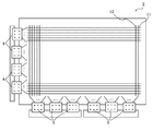
- FIG. 1 is a diagram illustrating a schematic configuration of a display panel according to the first embodiment.
- FIG. 2 is a diagram showing a schematic configuration of the active matrix substrate in the first embodiment.
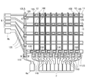
- FIG. 3A shows a schematic configuration diagram in which a part of the active matrix substrate of FIG. 2 is enlarged.
- FIG. 3B shows an equivalent circuit corresponding to one pixel portion of FIG. 3A.
- FIG. 4 is an enlarged plan view of one pixel portion of FIG. 3A.
- FIG. 5 is a cross-sectional view taken along the line A-A ′ of FIG.
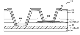
- FIG. 6 is a cross-sectional view of the SG contact portion in FIG. 3A cut along B-B ′.
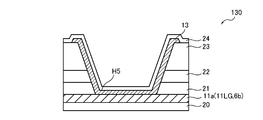
- FIG. 7 is a cross-sectional view of the G-COM contact portion in FIG.
- FIG. 9A is a diagram illustrating a manufacturing process of the TFT-PIX contact part in the first embodiment.
- FIG. 9B is a diagram illustrating a manufacturing process of the TFT-PIX contact part in the first embodiment.
- FIG. 9C is a diagram illustrating a manufacturing process of the TFT-PIX contact part in the first embodiment.
- FIG. 9D is a diagram illustrating a manufacturing process of the TFT-PIX contact part in the first embodiment.
- FIG. 9E is a diagram illustrating a manufacturing process of the TFT-PIX contact part in the first embodiment.
- FIG. 9F is a diagram illustrating a manufacturing process of the TFT-PIX contact part in the first embodiment.
- FIG. 9G is a diagram illustrating a manufacturing process of the TFT-PIX contact part in the first embodiment.
- FIG. 9H is a diagram illustrating a manufacturing process of the TFT-PIX contact part in the first embodiment.
- FIG. 9I is a diagram illustrating a manufacturing process of the TFT-PIX contact part in the first embodiment.
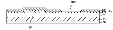
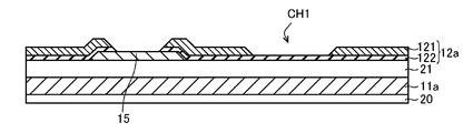
- FIG. 10A is a diagram illustrating another manufacturing process for forming the TFT-PIX contact portion.
- FIG. 10B is a diagram illustrating another manufacturing process for forming the TFT-PIX contact portion.
- FIG. 10C is a diagram illustrating another manufacturing process for forming the TFT-PIX contact portion.
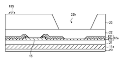
- FIG. 10A is a diagram illustrating another manufacturing process for forming the TFT-PIX contact portion.
- FIG. 10B is a diagram illustrating another manufacturing process for forming the TFT-PIX contact portion.
- FIG. 10D is a diagram illustrating another manufacturing process for forming the TFT-PIX contact portion.
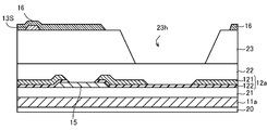
- FIG. 10E is a diagram illustrating another manufacturing process for forming the TFT-PIX contact portion.
- FIG. 10F is a diagram illustrating another manufacturing process for forming the TFT-PIX contact portion.
- FIG. 10G is a diagram illustrating another manufacturing process for forming the TFT-PIX contact portion.
- FIG. 10H is a diagram illustrating another manufacturing process for forming the TFT-PIX contact portion.
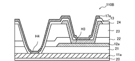
- FIG. 11 is a view showing a cross section of the SG contact portion in the second embodiment.
- FIG. 12 is a view showing a cross section of the SG contact portion in the third embodiment.
- a semiconductor device includes a semiconductor layer formed so as to overlap the plurality of gate wirings via a gate insulating film that covers the plurality of gate wirings formed on the substrate, and the gate wiring.
- a semiconductor device comprising: a plurality of drain wirings formed in a part of the semiconductor layer; and a thin film transistor in which a channel region is formed between the source wiring and the drain wiring on the semiconductor layer, the source wiring and A first contact hole penetrating a first interlayer insulating film covering the drain wiring and the channel region and a planarizing film covering the first interlayer insulating film.
- the film is made of a metal whose standard electrode potential is higher than that of the pixel electrode, or a metal whose potential difference from the standard electrode potential of the pixel electrode is within a predetermined range.
- the common electrode auxiliary wiring supplies a potential corresponding to a signal input to the common electrode.
- First configuration since the pixel electrode and the drain wiring are electrically connected via the drain connection film formed of the metal film that suppresses the electrolytic corrosion of ITO, aluminum having a low resistance as the drain wiring is provided. System metal wiring can be used. Further, the drain connection film and the common electrode auxiliary wiring are formed in the same layer using the same metal film. Therefore, the drain connection film can be formed in the process of forming the common electrode auxiliary wiring without increasing the number of manufacturing processes. In addition, since the potential can be supplied to the common electrode by the common electrode auxiliary wiring, the potential of the common electrode can be stabilized.
- a first terminal that inputs a gate signal to the gate wiring, a second terminal that inputs a source signal to the source wiring, and a potential to the common electrode are input.
- the first terminal, the second terminal, the third terminal, and the fourth terminal are formed in the same layer using a conductive film of the gate wiring, A first contact portion that electrically connects one source wiring of the source wirings to the third terminal and electrically connects the other source wiring and the second terminal;
- One gate line is electrically connected to the fourth terminal, and the other gate line is electrically connected to the first terminal, and the common line overlaps the one gate line and the other source line.
- Electrically connecting the electrode auxiliary wiring A contact portion, said and one source line may be a third contact portion for connecting said gate wiring and substantially parallel the common electrode auxiliary wiring electrically are formed.
- the one source wiring and the third terminal, and the other source wiring and the second terminal are the common electrode auxiliary wiring and the drain.
- the common electrode auxiliary wiring which is electrically connected through the metal film formed in the same layer as the connection film and overlaps the one gate wiring and the other source wiring in the second contact portion,
- the common electrode that is connected via the metal film formed in the same layer as the common electrode auxiliary wiring and the drain connection film, and is substantially parallel to the one source wiring and the gate wiring in the third contact portion
- the auxiliary wiring may be connected via the common electrode auxiliary wiring and the metal film formed in the same layer as the drain connection film.
- the common electrode auxiliary line can be connected to the gate line and the source line in the step of forming the common electrode auxiliary line and the drain connection film without increasing the number of manufacturing steps.
- the one source wiring and the third terminal, and the other source wiring and the second terminal are the third terminal and the second terminal.
- the common electrode auxiliary wiring that is formed so as to come into contact with the contact hole of the gate insulating film formed thereon and overlaps the one gate wiring and the other source wiring in the second contact portion,
- the common electrode auxiliary line connected to the common electrode auxiliary line and the metal film formed in the same layer as the drain connection film, and substantially parallel to the one source line and the gate line in the third contact portion.
- the wiring may be connected via the metal film formed in the same layer as the common electrode auxiliary wiring and the drain connection film.
- the semiconductor layer is formed of an oxide semiconductor
- the common electrode and the pixel electrode are formed of a transparent conductive film
- the source wiring and the drain wiring are Further, it may be composed of aluminum or a metal compound containing aluminum.
- the oxide semiconductor may be made of indium, gallium, zinc, and oxygen.
- a display panel includes an active matrix substrate including a semiconductor device having any one of the first to sixth configurations, a counter substrate including a color filter, the active matrix substrate, and the counter substrate. And a liquid crystal layer sandwiched therebetween (seventh configuration).
- a manufacturing method of a semiconductor device is a manufacturing method of a semiconductor device including a thin film transistor, and includes (A) a step of forming a thin film transistor on a substrate, and includes a gate line and a gate electrode. Forming a gate layer, a gate insulating film covering the gate layer, and a semiconductor layer covering a part of the gate insulating film; forming a source layer on the semiconductor layer; Forming a drain wiring including an electrode; (B) forming a first interlayer insulating film covering the source layer; and a planarizing film covering the first interlayer insulating film; and (C) the planarizing.
- etching the first interlayer insulating film to form a first contact hole exposing the drain electrode and (D) forming a metal film on the planarizing film, Forming a drain connection film so as to be in contact with the drain wiring in one contact hole, and forming a common electrode auxiliary wiring at a position overlapping with a part of the source line; and (E) covering the common electrode auxiliary wiring; Forming a common electrode at a position outside a region where the drain connection film is formed; and (F) forming a second interlayer insulating film on the common electrode and the drain connection film; and Etching to form a second contact hole that exposes the drain connection film inside the first contact hole, and (G) the second contact hole so as to be in contact with the drain connection film.
- Electrode potential higher metals, or metal of the range difference between the standard electrode potential of the pixel electrode is determined in advance is configured to contact with the pixel electrode (eighth configuration).
- FIG. 1 is a diagram showing a schematic configuration of a display panel of a liquid crystal display device having a semiconductor device according to the present embodiment.
- the display panel 1 includes an active matrix substrate 2, a counter substrate 3, and a liquid crystal layer (not shown) sandwiched between these substrates.
- a color filter substrate (not shown) is formed on the counter substrate 3 shown in FIG.
- the display panel 1 is irradiated with light from a backlight (not shown) provided on the back side of the active matrix substrate 2.
- the active matrix substrate 2 is provided with a gate driver 4 and a source driver 5.
- the display panel 1 drives the liquid crystal in the liquid crystal layer based on the data signal and the scanning signal output from the source driver 4 and the gate driver 5 according to the external input signal, and displays an image in the display area.
- the gate driver 4 and the source driver 5 are configured by TAB (Tape Automated Automated Bonding) in which the semiconductor chips of the gate driver 4 and the source driver 5 are mounted on a film such as polyimide.
- TAB Tepe Automated Automated Bonding
- Each gate driver 4 and each source driver 5 are electrically connected to the active matrix substrate 2 and also electrically connected to the respective printed circuit boards 4P and 5P.
- Each gate driver 4 and each source driver 5 are supplied with external input signals such as timing signals and image signals from a control circuit (not shown) via a printed circuit board 6 connected to each gate driver 4 and each source driver 5.
- FIG. 2 is a diagram showing a schematic configuration of the active matrix substrate 2.
- FIG. 3A shows a schematic configuration diagram in which a part of the active matrix substrate 2 is enlarged.
- a gate line group 11 connected to each gate driver 4 and a source line group 12 connected to each source driver 5 are formed on the substrate 20 of the active matrix substrate 2.
- the gate lines 11 are formed in parallel toward one direction of the substrate 20.
- the source line 12 intersects with the gate line 11 and is formed in parallel.
- a region surrounded by each gate line 11 and each source line 12 forms one pixel, and a pixel region including all pixels forms a display region of the display panel 1.
- a terminal group 7 and a terminal group 8 are formed outside the display area of the active matrix substrate 2.
- the terminal group 7 inputs a source signal input from the source driver 5 to the source line 12.
- the terminal group 8 inputs a gate signal input from the gate driver 4 to the gate line 11.
- a common electrode 16 (see FIG. 5) and a pixel electrode 17 (see FIG. 5), which will be described later, are formed in the display area of the active matrix substrate 2.
- the display panel 1 drives the liquid crystal by a lateral electric field method called IPS (In Plane Switching) or FFS (fringe field switching).
- terminals 6 (6a, 6b), wirings 12LS and wirings 11LG are formed on the active matrix substrate 2.
- the terminal 6 inputs a potential to the common electrode 16.
- the wiring 12LS is connected to the terminal 6a, and the wiring 11LG is connected to the terminal 6b.
- Each terminal 6, 7, 8 and wiring 11 LG are formed in the same layer as the gate line 11 using the same conductive film as the gate line 11.
- the wiring 12LS is formed in the same layer as the source line 12 using the same conductive film as the source line 12.
- the terminal 6a and the wiring 12LS are connected via a contact hole.
- Each terminal 7 and each source line 12 are connected via a contact hole.
- the terminal 6b and the wiring 11LG, the terminals 8 and the gate lines 11 are integrally formed and are electrically connected to each other.
- the gate line 11 and the wiring 11LG are examples of gate wiring
- the source line 12 and the wiring 12LS are examples of source wiring.
- FIG. 3B shows an equivalent circuit corresponding to one pixel portion of FIG. 3A.
- a TFT 14 Thin Film Transistor
- a capacitor Cl is formed by the pixel electrode 17 and the common electrode 16.
- the TFT 14 and the pixel electrode 17 are electrically connected via a contact hole.
- auxiliary wirings 13S and 13G are formed on the active matrix substrate 2.
- the auxiliary wirings 13 ⁇ / b> S and 13 ⁇ / b> G supply the potential input from each terminal 6 to the common electrode 16.
- the auxiliary wiring 13 ⁇ / b> S overlaps with the source line 12 and is formed so as to intersect with the gate line 11.
- the auxiliary wiring 13G is formed substantially parallel to the gate line 11 in the vicinity of each gate line 11 so as to overlap a part of the wiring 12LS.
- the wiring 12LS and each auxiliary wiring 13G are electrically connected to a part of the auxiliary wiring 13G through a contact hole.
- the wiring 11LG and each auxiliary wiring 13S are electrically connected to a part of the auxiliary wiring 13S through a contact hole.
- the auxiliary wirings 13S and 13G in the present embodiment are examples of common electrode auxiliary wirings.
- a region 100 where the TFT 14 and the pixel electrode (not shown in FIG. 3A) overlap is a connection portion between the TFT 14 and the pixel electrode 17, and is hereinafter referred to as a TFT-PIX contact portion 100.
- a region 110 where the wiring 12LS and each source line 12 and each terminal (6a, 7) overlap the wiring 12LS and the terminal 6a, and each source line 12 and each terminal 7 are connected via a contact hole. It is a connection part.
- the SG contact portion 110 is referred to.
- a region 120 where the auxiliary wiring 13G and the wiring 12LS overlap is a connection portion between the wiring 12LS and the auxiliary wiring 13G.
- an S-COM contact part 120 A region 130 where the wiring 11LG and the auxiliary wiring 13S overlap is a connection portion between the wiring 11LG and the auxiliary wiring 13S.
- the region 130 is referred to as a G-COM contact part 130.
- the source signal input from each terminal 7 is transmitted to the source line 12 via the SG contact portion 110.
- the potential to the common electrode 16 input from the terminal 6a is transmitted to the auxiliary wiring 13G via the SG contact part 110 and the S-COM contact part 120 in the wiring 12LS.
- the potential to the common electrode 16 input from the terminal 6b is transmitted to the auxiliary wiring 13S via the G-COM contact part 130.
- FIG. 4 is an enlarged plan view of one pixel portion of FIG. 3A.
- the TFT 14 includes a source electrode 12S, a gate electrode 11G, a drain electrode 12D, and a semiconductor portion 15.
- the pixel electrode 17 is formed in each pixel region and has an opening 17A.
- the pixel electrode 17 is electrically connected to the drain electrode 12D of the TFT 14.
- the common electrode 16 (see FIG. 5) is omitted, but the common electrode 16 is formed on the lower side of the pixel electrode 17 and outside the opening 16h of the common electrode 16 indicated by a broken line. Yes. That is, the common electrode 16 is formed in the entire pixel region except for the region of the TFT-PIX contact portion 100 where the drain electrode 12D and the pixel electrode 17 are connected.
- FIG. 5 is a cross-sectional view taken along the line A-A ′ of FIG.
- a gate layer 11a is formed on a substrate 20 having transparency and insulating properties such as glass.
- the gate layer 11a is made of, for example, a metal such as copper (Cu), aluminum (Al), titanium (Ti), molybdenum (Mo), or an alloy thereof.
- the gate line 11 and the gate electrode 11G are integrally formed.
- a gate insulating film 21 made of a silicon nitride film (SiNx), a silicon oxide film (SiO2), or the like is formed on the gate layer 11a.
- a semiconductor portion 15 is formed on the gate insulating film 21.
- the semiconductor portion 15 is made of amorphous silicon (a-Si), polysilicon (poly-Si), an oxide semiconductor, or the like.
- a source layer 12 a is formed on the upper portion of the semiconductor portion 15.
- the source layer 12a is made of, for example, a single layer film of Al or a laminated film having Al as an upper layer and Ti as a lower layer.
- the source line 12 and the source electrode 12S are integrally formed, and the drain electrode 12D is formed.
- the source electrode 12 ⁇ / b> S and the drain electrode 12 ⁇ / b> D are formed apart from each other in the upper part of the semiconductor portion 15.
- a channel region 15a is formed between the source electrode 12S and the drain electrode 12D in the upper part of the semiconductor portion 15.
- the source line 12 and the source electrode 12S are examples of source wiring
- the drain electrode 12D is an example of drain wiring.
- An interlayer insulating film 22 and a planarizing film 23 are stacked on the source electrode 12S, the drain electrode 12D, and the channel region 15a.
- a contact hole H1 is formed in the interlayer insulating film 22 and the planarizing film 23 above the drain electrode 12D.
- the interlayer insulating film 22 is composed of an inorganic insulating film.
- the planarizing film 23 is composed of an organic insulating film.
- An auxiliary wiring layer 13 is formed on the flattening film 23.
- a metal film that suppresses electrolytic corrosion between the auxiliary wiring layer 13 and the pixel electrode 17 is used.
- the metal film for example, a laminated film in which Cu, Ti, Mo or the like is the uppermost layer that is in direct contact with the pixel electrode 17 is used.
- the reference electrode is a standard hydrogen electrode in an aqueous solution at 25 ° C.
- the standard electrode potential of ITO used as the pixel electrode 17 is 0.03V.
- the metal film used for the auxiliary wiring layer 13 is made of a metal whose standard electrode potential is higher than that of the pixel electrode 17 or a metal whose potential difference from the standard electrode potential of the pixel electrode 17 is within a predetermined range. What is necessary is just to be comprised so that it may touch.
- the potential difference between the standard electrode potential and the pixel electrode 17 may be, for example, within 1.66V.
- the auxiliary wiring 13S and the drain connection film 13P are formed.
- the auxiliary wiring 13S is formed at a position overlapping the source line 12 with the interlayer insulating film 22 and the planarizing film 23 interposed therebetween.
- the drain connection film 13P is formed in the contact hole H1 so as to be in contact with the drain electrode 12D.
- the auxiliary wiring 13G parallel to the gate line 11 is formed simultaneously with the auxiliary wiring 13G and the drain connection film 13P.
- the common electrode 16 is formed on the planarizing film 23.
- the common electrode 16 has an opening 16h so as not to contact the drain connection film 13P in the upper layer of the planarizing film 23, and is formed so as to cover the auxiliary wiring 13S.
- An interlayer insulating film 24 is formed on the common electrode 16 so as to cover the common electrode 16 and the drain connection film 13P, and a contact hole H2 is formed.
- a pixel electrode 17 is formed so as to cover a part of the interlayer insulating film 24 in the contact hole H2.
- the interlayer insulating film 24 is composed of an inorganic insulating film.
- the common electrode 16 and the pixel electrode 17 are made of a transparent conductive film such as ITO.
- the drain electrode 12D and the pixel electrode 17 are electrically connected via the drain connection film 13P, and the TFT-PIX contact portion 100 is formed.
- the auxiliary wiring layer 13 is made of a material that suppresses electrolytic corrosion with the pixel electrode 17.
- the drain connection film 13P is in direct contact with the pixel electrode 17. Therefore, even when the drain electrode 12 ⁇ / b> D is composed of an aluminum-based metal film, the occurrence of electrolytic corrosion between the drain connection film 13 ⁇ / b> P and the pixel electrode 17 can be prevented.
- FIG. 6 is a cross-sectional view of the SG contact portion 110 in FIG. 3A cut along B-B ′.
- the gate layer 11 a is formed on the substrate 20.
- the terminals 6a and 7 are formed by forming the gate layer 11a.
- a source layer 12a is formed on the gate layer 11a with a gate insulating film 21 therebetween.
- a wiring 12LS and a source line 12 are formed by forming the source layer 12a.
- An interlayer insulating film 22 is formed so as to cover the source layer 12 a, and a planarizing film 23 is formed on the interlayer insulating film 22.
- a contact hole H3 is formed in the portion of the planarizing film 23 and the interlayer insulating film 22 on the source layer 12a.
- a contact hole H4 is formed in the planarizing film 23, the interlayer insulating film 22, and the gate insulating film 21 except for the source layer 12.
- An auxiliary wiring layer 13 is formed on the planarizing film 23 so as to connect the contact holes H3 and H4.
- the interlayer insulating film 24 is formed so as to cover the auxiliary wiring layer 13.
- the wiring 12LS (source layer 12a) and the terminal 6a (gate layer 11a) are electrically connected through the auxiliary wiring layer 13 formed in the contact holes H3 and H4.
- the source line 12 (source layer 12a) and the terminal 7 (gate layer 11a) are electrically connected through the auxiliary wiring layer 13. Therefore, the source signal input from the terminal 7 can be transmitted to the source line 12 through the auxiliary wiring layer 13.
- FIG. 7 is a cross-sectional view of the G-COM contact portion 130 in FIG. 3A cut along C-C ′.
- a gate layer 11 a is formed on the substrate 20.
- the terminal 6b and the wiring 11LG are integrally formed.
- a gate insulating film 21, an interlayer insulating film 22, and a planarizing film 23 are formed in this order on the gate layer 11a.
- a contact hole H5 exposing the gate layer 11a is formed in the gate insulating film 21, the interlayer insulating film 22, and the planarizing film 23, a contact hole H5 exposing the gate layer 11a is formed.
- An auxiliary wiring layer 13 is formed on the planarizing film 23.
- the auxiliary wiring layer 13 is in contact with the gate layer 11a in the contact hole H5.
- the interlayer insulating film 24 is formed so as to cover the auxiliary wiring layer 13.
- the wiring 11LG formed integrally with the terminal 6b is electrically connected to the common electrode 16 through the auxiliary wiring layer 13 formed in the contact hole H5. Therefore, the potential input from the terminal 6b can be supplied to the common electrode 16 via the auxiliary wiring layer 13, and the potential of the common electrode 16 can be stabilized.
- FIG. 8 is a cross-sectional view of the S-COM contact portion 120 in FIG. 3A cut along D-D ′.
- the source layer 12 a is formed on the substrate 20 via the gate insulating film 21.
- the wiring 12LS is formed by forming the source layer 12a.
- An interlayer insulating film 22 and a planarizing film 23 are formed in this order on the source layer 12a.
- a contact hole H6 is formed in the interlayer insulating film 22 and the planarizing film 23.
- An auxiliary wiring layer 13 is formed on the planarizing film 23.
- the auxiliary wiring layer 13 is in contact with the source layer 12a in the contact hole H6.
- the interlayer insulating film 24 is formed so as to cover the auxiliary wiring layer 13.
- the wiring 12LS (source layer 12a) and the common electrode 16 are electrically connected via the auxiliary wiring layer 13 formed in the contact hole H6. Therefore, the potential input from the terminal 6a is transmitted to the wiring 12LS (source layer 12a) via the SG contact portion 110 shown in FIG. 6, and from the wiring 12LS (source layer 12a) via the auxiliary wiring layer 13. It is supplied to the common electrode 16.
- 9A to 9I are views showing a process of forming the TFT-PIX contact portion 100 shown in FIG. 5, and are cross-sectional views taken along line AA ′ of FIG.
- eight masks are used in the following steps (1) to (10).
- the processing of each step of the TFT-PIX contact unit 100 will be described, and the formation of the SG contact unit 110, the S-COM contact unit 120, and the G-COM contact unit 130 will be described together.
- Gate Layer 11a As shown in FIG. 9A, a conductive film for the gate layer 11a is formed on the substrate 20 by sputtering. Then, in a region where the TFT 14 is formed, a resist mask is formed using photolithography to create a resist pattern. Further, patterning is performed by removing a portion of the conductive film not covered with the resist mask by wet etching or dry etching. This is the first mask process. Thereby, the gate electrode 11G and the gate line 11 are integrally formed. Similarly, in the SG contact part 110 and the G-COM contact part 130, as shown in FIGS. 6 and 7, the terminals 6 and 7 and the wiring 11LG are formed on the substrate 20.
- the gate layer 11a for example, a film containing a metal such as Cu, Al, Ti, or Mo, an alloy thereof, or a nitride thereof is used.
- a laminated film in which the upper layer is Cu and the lower layer is Ti is used.
- the film thickness of the upper layer is, for example, 180 nm or more and 300 nm or less
- the film thickness of the lower layer is, for example, 15 nm or more and 35 nm or less.
- the gate insulating film 21 is formed on the substrate 20 on which the gate layer 11a is formed by a plasma CVD method or a sputtering method. Also in the S-G contact part 110, the G-COM contact part 130, and the S-COM contact part 120, the gate insulating film 21 is formed as shown in FIGS.
- the gate insulating film 21 for example, a silicon nitride film, a silicon oxide film, or a laminated film thereof is used.
- the film thickness of the gate insulating film 21 is, for example, not less than 200 nm and not more than 400 nm.
- a semiconductor is formed on the substrate 20 on which the gate insulating film 21 is formed by using a plasma CVD method or a sputtering method. Then, a resist pattern is created using photolithography, and wet etching or dry etching is performed. Thus, patterning is performed in an island shape as shown in FIG. 9C. This is the second mask process.
- the semiconductor for example, a-Si, poly-Si, or an oxide semiconductor such as IGZO or InGaO 3 (ZnO) 5 is used.
- the film thickness of the semiconductor unit 15 is, for example, 30 nm or more and 100 nm or less.
- a conductive film for the source layer 12a is formed on the substrate 20 on which the semiconductor portion 15 is formed by a sputtering method. Then, in a region where the source line 12 and the source electrode 12S and the drain electrode 12D are to be formed, a resist pattern is created using photolithography, and wet etching, dry etching, or etching combining them is performed. This is the third mask process.
- the source line 12, the source electrode 12S, and the drain electrode 12D are formed so that the source electrode 12S and the drain electrode 12 are separated from each other on the semiconductor 15.
- the wiring 12LS is formed on the gate insulating film 21 as shown in FIGS.
- a metal film including a metal such as Al, Mo, Cu, Ti, tantalum (Ta), tungsten (W), an alloy thereof, or a metal nitride thereof is used.
- a laminated film having an upper layer made of Al and a lower layer made of Ti is used.
- the film thickness of the source layer 12a is, for example, not less than 180 and not more than 300 nm.
- the interlayer insulating film 22 is formed on the substrate 20 on which the source layer 12a is formed by using a plasma CVD method or a sputtering method. Form a film. Then, an opening (not shown) of the planarizing film 23 is formed on the substrate 20 on which the interlayer insulating film 22 is formed by patterning the planarizing film 23 using photolithography. This is the fourth mask process.
- the interlayer insulating film 22 for example, an inorganic insulating film such as a silicon nitride film or a silicon oxide film, or a laminated film thereof is used.
- planarizing film 23 for example, an organic insulating film such as a positive photosensitive resin film is used.
- the thickness of the interlayer insulating film 22 is, for example, not less than 200 nm and not more than 300 nm.
- the thickness of the planarizing film 23 is, for example, 2 ⁇ m or more and 3 ⁇ m or less.
- the interlayer insulating film 22 is etched by dry etching using the planarizing film 23 as a mask. As a result, as shown in FIG. 9F, a contact hole H1 is formed. Thereby, the surface of the drain electrode 12D is exposed.
- the contact holes H3, H6 simultaneously with the formation of the contact hole H1, the contact holes H3, H6 exposing the source layer 12a also in the SG contact portion 110 and the G-COM contact portion 130. Is formed.
- the interlayer insulating film 22 and the gate insulating film 21 are simultaneously etched using the planarizing film 23 as a mask. As a result, contact holes H4 and H5 are formed.
- a conductive film for the auxiliary wiring layer 13 is formed by sputtering on the substrate 20 on which the planarizing film 23 is formed and the surface of the drain electrode 12D is exposed. Then, in a region where the auxiliary wirings 13S and 13G are to be formed, a resist pattern is created using photolithography, and patterning is performed by performing wet etching, dry etching, or etching combining them. This is the fifth mask process. As a result, as shown in FIG. 9G, the drain connection film 13P is formed in the contact hole H1, and the auxiliary wiring 13S is formed at a position overlapping the source line 12 via the interlayer insulating film 22 and the planarization film 23.
- the drain connection film 13P and the auxiliary wiring 13S are formed simultaneously.
- the auxiliary wiring layer 13 is formed in each of the contact holes H3, 4, 5, and 6.
- the layer in contact with the pixel electrode is a metal having a higher standard electrode potential than ITO used for the pixel electrode 17, or the difference from the standard electrode potential of the pixel electrode 17 is within a predetermined range.
- the metal may be the outermost surface.
- it may be a laminated film of two layers made of Cu / Ti or Cu / Mo with Cu, Ti and Mo as the outermost surface, or a three-layered film made of Mo / Al / Mo or Ti / Al / Ti A laminated film may be used.
- the thickness of the auxiliary wiring layer 13 is, for example, not less than 200 nm and not more than 350 nm.
- a transparent conductive film is formed on the substrate 20 on which the auxiliary wiring layer 13 is formed using a sputtering method. Then, in a region where the common electrode 16 is to be formed, a resist pattern is formed using photolithography, and patterning is performed by etching using wet etching. This is the sixth mask process. As a result, as shown in FIG. 9H, the opening 16h of the common electrode 16 is formed, and the common electrode 16 is formed outside the opening 16h.
- the common electrode 16 for example, a transparent conductive film such as ITO (indium tin oxide) or IZO (indium zinc oxide) is used.
- the film thickness of the common electrode 16 is, for example, 60 nm or more and 120 nm or less. Note that the resistance may be reduced by baking the common electrode 16 after patterning.
- An interlayer insulating film 24 is formed on the substrate 20 on which the common electrode 16 is formed by using a plasma CVD method or a sputtering method. Then, a resist pattern is formed using photolithography, and patterning is performed by etching using dry etching. This is the seventh mask process. As a result, as shown in FIG. 9I, a contact hole H2 is formed inside the contact hole H1, and an interlayer insulating film 24 is formed on the common electrode 16. Similarly, as shown in FIGS. 6, 7, and 8, the SG contact portion 110, the G-COM contact portion 130, and the S-COM contact portion 120 also have an interlayer above the auxiliary wiring layer 13. An insulating film 24 is formed.
- the interlayer insulating film 24 for example, an inorganic insulating film such as a silicon nitride film or a silicon oxide film, or a laminated film thereof is used.
- the film thickness of the interlayer insulating film 24 is, for example, not less than 100 nm and not more than 300 nm.
- the contact hole H1 is an example of a first contact hole
- the contact hole H2 is an example of a second contact hole.
- a transparent conductive film is formed on the substrate 20 on which the interlayer insulating film 24 is formed using a sputtering method. Then, in a region where the pixel electrode 17 is to be formed, a resist pattern is formed using photolithography, and patterning is performed by etching using wet etching. This is the eighth mask process. Thereby, as shown in FIG. 5, the pixel electrode 17 is formed so as to overlap a part of the interlayer insulating film 24 and the drain connection film 13P. The pixel electrode 17 is electrically connected to the drain electrode 12D through the drain connection film 13P. Note that the resistance may be reduced by performing a baking process on the pixel electrode 17 after patterning.
- the pixel electrode 17 is made of an oxide thin film such as ITO (indium / tin oxide) or IZO (indium / zinc oxide).
- the film thickness of the pixel electrode 17 is, for example, 60 nm or more and 120 nm or less.
- a metal film that suppresses electrolytic corrosion with the pixel electrode 17 is used for the drain connection film 13P. Since the pixel electrode 17 and the drain electrode 12D are not in direct contact with each other, it is possible to prevent electrolytic corrosion from occurring between the drain electrode 12D and the drain connection film 13P when the pixel electrode 17 is formed.
- the drain connection film 13P is formed so as not to generate electrolytic corrosion with the drain electrode 12D when the pixel electrode 17 is formed.
- another configuration for preventing the electrolytic corrosion of the pixel electrode 17 without forming the drain connection film 13P will be considered.
- only the auxiliary wiring 13S for stabilizing the potential of the common electrode 16 is formed. 10A to 10H illustrate the manufacturing process having such a configuration.
- the semiconductor portion 15 is formed on the gate insulating film 21 by the method of the above steps (1) to (3). Then, patterning is performed using photolithography in a state in which the source layer 12 a having aluminum as the upper layer 121 and titanium as the lower layer 122 is formed so as to cover the semiconductor portion 15. Further, only the upper layer 121 of the source layer 12a is etched to expose the lower layer 122. As a result, as shown in FIG. 10B, a contact hole CH1 is formed in the source layer 12a (step (4 ′)).
- the interlayer insulating film 22 is formed by the method of step (5) of the above embodiment, and the planarizing film 23 is patterned using photolithography, so that the planarizing film 23 is formed as shown in FIG. 10C. Opening 23h is formed.
- the auxiliary wiring layer 13 is formed in the same manner as in step (6) of the above embodiment, and is patterned and etched using photolithography at a position overlapping the source line 12. Thereby, the auxiliary wiring 13S is formed as shown in FIG. 10D. Then, similarly to step (7) of the above embodiment, patterning is performed using photolithography in the region where the common electrode 16 is to be formed, and etching is performed. Thereby, the common electrode 16 is formed as shown in FIG. 10E.
- an interlayer insulating film 24 is formed on the common electrode 16 as in the step (8). Then, patterning is performed using photolithography, and the interlayer insulating film 24 and the interlayer insulating film 22 are simultaneously etched. As a result, as shown in FIG. 10G, a contact hole CH2 is formed and the lower layer 122 of the source layer 12a is exposed. Subsequently, patterning is performed using photolithography in the same manner as in step (9). Thereby, as shown in FIG. 10H, the pixel electrode 17 is formed in the upper layer of the interlayer insulating film 24 so as to cover the contact hole CH2.
- the drain connection film 13P when the drain connection film 13P is not formed, the upper layer 121 of the source layer 12a is removed and the lower layer 122 and the pixel electrode 17 are brought into direct contact with each other. That is, aluminum that causes electrolytic corrosion with the pixel electrode 17 does not come into contact with the pixel electrode 17, but directly contacts titanium with the pixel electrode 17. Thereby, the pixel electrode 17 and the drain electrode 12D (source layer 12a) are electrically connected, and the electrolytic corrosion of the pixel electrode 17 and the drain electrode 12D is prevented.
- step (4 ′) is required in addition to the steps (1) to (9).
- step (4 ′) a contact hole CH1 for exposing the lower layer 122 of the source layer 12a is formed. Therefore, in the processes of FIGS. 10A to 10H, a separate mask is required in step (4 ′). As a result, the number of masks is one more than in the embodiment described above.
- the drain connection film 13P is formed in the TFT-PIX contact portion 100 simultaneously with the formation of the auxiliary wiring 13S. Therefore, the pixel electrode 17 is formed on the drain connection film 13P and connected to the drain electrode 12D through the drain connection film 13P. As a result, it is not necessary to form the contact hole CH1 as in FIG. 10A, and the number of masks can be reduced as compared with the manufacturing process shown in FIGS. 10A to 10H.
- FIG. 11 is a view showing a cross section of the SG contact portion 110A in the present embodiment.
- patterning is performed using photolithography, and the gate insulating film 21 is dry-etched. Thereby, an opening is formed in the gate insulating film 21.
- the source layer 12a is formed in the opening.
- the interlayer insulating film 22, the planarizing film 23, and the interlayer insulating film 24 are sequentially formed in the processes of steps (5) and (8) of the first embodiment.
- the auxiliary wiring layer 13 for connecting the gate layer 11a and the source layer 12a is formed simultaneously with the drain connection film 13P. Therefore, it is not necessary to separately use a mask for connecting the gate layer 11a and the source layer 12a.
- a mask for forming an opening for directly contacting the gate layer 11a and the source layer 12a is required before the source layer 12a is formed.
- the gate layer 11a and the source layer 12a can be directly connected. As a result, the area of the SG contact portion 110 can be made smaller than in the case of the first embodiment, and the display panel can be narrowed.
- FIG. 12 is a view showing a cross section of the SG contact portion 110B in the present embodiment.
- this embodiment after forming the contact holes H3 and H4 in step (5) of the first embodiment described above, in the process of step (6), only the contact hole H3 is assisted. A wiring layer 13 is formed. Subsequently, in the process of step (8), an interlayer insulating film 24 is formed so as to cover the auxiliary wiring layer 13, the contact hole H4, and the planarizing film 23.
- the pixel electrode layer 17a is formed so as to cover the interlayer insulating film 24 at the same time as the pixel electrode 17 is formed.
- the pixel electrode layer 17 a is composed of the conductive film of the pixel electrode 17.
- the source layer 12 a and the pixel electrode layer 17 a are laminated via the auxiliary wiring layer 13. Since the auxiliary wiring layer 13 uses a metal that suppresses electrolytic corrosion with the pixel electrode 17, no electrolytic corrosion occurs when the pixel electrode layer 17 a is formed. Therefore, a low-resistance aluminum-based metal film can be used as the source layer 12a.
- the gate layer 11a and the source layer 12a are electrically connected via the pixel electrode layer 17a.
- the gate layer 11a is configured to use a material that suppresses electrolytic corrosion with ITO on the outermost surface that is in direct contact with the pixel electrode layer 17a, like the auxiliary wiring layer 13.
- the potential of the common electrode 16 input from the terminal 6a is transmitted to the source layer 12a via the pixel electrode layer 17a and supplied to the common electrode 16 via the S-COM contact portion 120.
- the display panel 1 is a liquid crystal panel
- a panel using organic EL (Electro-Luminescence) or the like may be used.
- the auxiliary wiring 13G is formed in the vicinity of the gate line 11 so as to be parallel to the gate line 11 has been described. Also good. That is, the auxiliary wiring 13G may be formed on the gate line 11 as long as the auxiliary wiring 13G does not overlap the TFT-PIX contact portion 100.
- the auxiliary wirings 13S and 13G may be configured as follows.
- the auxiliary wiring 13G may be formed at a position near the predetermined gate line 11, and the auxiliary wiring 13S may be formed so as to overlap the predetermined source line 12.
- the auxiliary wiring 13G is formed at a position in the vicinity of a part of the gate lines 11 so that the potential to the common electrode 16 can be supplied to a plurality of pixel areas among all the pixel areas. It is sufficient if the auxiliary wiring 13S is formed so as to overlap.
- the present invention can be used industrially as a display panel such as a liquid crystal panel or an organic EL panel used in a display device.
Landscapes
- Physics & Mathematics (AREA)
- Nonlinear Science (AREA)
- Mathematical Physics (AREA)
- Chemical & Material Sciences (AREA)
- Crystallography & Structural Chemistry (AREA)
- General Physics & Mathematics (AREA)
- Optics & Photonics (AREA)
- Engineering & Computer Science (AREA)
- Microelectronics & Electronic Packaging (AREA)
- Liquid Crystal (AREA)
- Thin Film Transistor (AREA)
- Manufacturing & Machinery (AREA)
Abstract
本発明は、ソース-ドレイン配線として、ITOとの直接接触が困難な金属配線を用いた場合であっても、TFT基板の製造工程を増加させることなく電食の発生を抑制する。半導体装置は、基板20上に形成されたゲート電極を含むゲート層11aと、ゲート層11a上にゲート絶縁膜21を介して形成された半導体部15と、半導体部15の上にソース電極とドレイン電極とを含むソース層12aとを有するTFTを備える。半導体装置は、ソース層12aの上に積層された層間絶縁膜22と平坦化膜23に形成されたコンタクトホールH1と、ソース線と重なる位置に、ITOとの電食を抑制する金属からなる補助配線層13Pと13Sが形成され、補助配線層13Pを介して画素電極17とドレイン電極12Dとが接続されている。補助配線層13S上には共通電極16が形成され、補助配線層13Sを介して共通電極16に電位が供給される。
Description
本発明は、薄膜トランジスタ(TFT(Thin Film Transistor))を用いた半導体装置、表示パネル、及び半導体装置の製造方法に関する。
従来より、TFTを用いた液晶表示装置において、画素内に補助容量コンデンサCsを設け、補助容量コンデンサCsの補助配線を設けているものがある。中でもFFS(Fringe Field Switching)構造の液晶表示装置においては、共通電極の電位を安定化させるために、画素内に配置された補助容量電極と共通電極とをある間隔にて接続しているものがある。しかしながら、特に高精細な表示パネルの場合においては高い開口率が求められており、画素内に補助容量コンデンサや補助配線を形成することが難しい。そのため、画素内に配置された補助容量電極との接続による共通電極の電位安定化を図ることが難しい。
特開2010-231035号公報の液晶表示装置には、金属膜で構成された共通電極補助線CRMが形成されている。共通電極補助線CRMを用いることによって、共通電極に電圧を印加する際の電気抵抗を低下することができるため共通電極の電位を安定させることができる。このため、画素内に補助容量電極や補助配線を形成する必要がない。また、共通電極補助線はゲート信号線GLやドレイン信号線DLと重畳する位置に形成されているため、画素領域内に補助容量配線等が形成されている場合と比べて開口率が向上する。
ところで、TFTにおけるソース-ドレイン配線としてアルミニウム配線又はアルミニウムを主体とする金属配線が用いられることがある。このようなアルミニウム系の金属配線をソース-ドレイン配線として有するTFT基板に、画素電極あるいは共通電極としてITO(Indium Tin Oxide)などの透明導電膜をスパッタ法で成膜すると、ITOと金属配線との間に電食が発生する。上記特開2010-231035号公報において、ソース信号線及びドレイン信号線にアルミニウム系の金属配線を用いた場合も同様である。
本発明は、ソース-ドレイン配線として、ITOとの直接接触が困難な金属配線を用いた場合であっても、TFT基板の製造工程を増加させることなく電食の発生を抑制する技術を提供することを目的とする。
本発明による半導体装置は、基板に形成された複数のゲート配線を覆うゲート絶縁膜を介して前記複数のゲート配線と重なるように形成された半導体層と、前記ゲート配線と交差するように前記ゲート絶縁膜及び前記半導体層の一部の上に形成された複数のソース配線と、前記半導体層上で前記ソース配線と離間し、前記ゲート配線と重なるように前記ゲート絶縁膜及び前記半導体層の一部に形成された複数のドレイン配線と、前記半導体層上における前記ソース配線及び前記ドレイン配線の間にチャネル領域が形成された薄膜トランジスタを備える半導体装置であって、前記ソース配線及び前記ドレイン配線と前記チャネル領域とを覆う第1層間絶縁膜と、前記第1層間絶縁膜を覆う平坦化膜とを貫通する第1コンタクトホールを介して前記ドレイン配線と電気的に接続される金属膜からなるドレイン接続膜と、前記ソース配線の少なくとも一部と重なると共に、前記複数のゲート配線の少なくとも一部の近傍において前記ゲート配線と略平行に形成された前記金属膜からなる共通電極補助配線と、前記共通電極補助配線の少なくとも一部と重なるように形成され、前記共通電極補助配線と電気的に接続される共通電極と、前記第1コンタクトホールの内側であって、前記ドレイン接続膜を覆う第2層間絶縁膜に設けられた第2コンタクトホールにおいて、前記ドレイン接続膜と電気的に接続される画素電極とを備え、前記金属膜は、前記画素電極より標準電極電位が高い金属、又は、前記画素電極の標準電極電位との電位差が予め定めた範囲内となる金属が前記画素電極と接するように構成され、前記共通電極補助配線は、入力される信号に応じた電位を前記共通電極に供給する。
本発明の半導体装置は、ソース-ドレイン配線として、ITOとの直接接触が困難な金属配線を用いた場合であっても、TFT基板の製造工程を増加させることなく電食の発生を抑制することができる。
本発明の一実施形態に係る半導体装置は、基板に形成された複数のゲート配線を覆うゲート絶縁膜を介して前記複数のゲート配線と重なるように形成された半導体層と、前記ゲート配線と交差するように前記ゲート絶縁膜及び前記半導体層の一部の上に形成された複数のソース配線と、前記半導体層上で前記ソース配線と離間し、前記ゲート配線と重なるように前記ゲート絶縁膜及び前記半導体層の一部に形成された複数のドレイン配線と、前記半導体層上における前記ソース配線及び前記ドレイン配線の間にチャネル領域が形成された薄膜トランジスタを備える半導体装置であって、前記ソース配線及び前記ドレイン配線と前記チャネル領域とを覆う第1層間絶縁膜と、前記第1層間絶縁膜を覆う平坦化膜とを貫通する第1コンタクトホールを介して前記ドレイン配線と電気的に接続される金属膜からなるドレイン接続膜と、前記ソース配線の少なくとも一部と重なると共に、前記複数のゲート配線の少なくとも一部の近傍において前記ゲート配線と略平行に形成された前記金属膜からなる共通電極補助配線と、前記共通電極補助配線の少なくとも一部と重なるように形成され、前記共通電極補助配線と電気的に接続される共通電極と、前記第1コンタクトホールの内側であって、前記ドレイン接続膜を覆う第2層間絶縁膜に設けられた第2コンタクトホールにおいて、前記ドレイン接続膜と電気的に接続される画素電極とを備え、前記金属膜は、前記画素電極より標準電極電位が高い金属、又は、前記画素電極の標準電極電位との電位差が予め定めた範囲内となる金属が前記画素電極と接するように構成され、前記共通電極補助配線は、入力される信号に応じた電位を前記共通電極に供給する。(第1の構成)。第1の構成によれば、ITOの電食を抑制する金属膜で構成されたドレイン接続膜を介して画素電極とドレイン配線とを電気的に接続しているので、ドレイン配線として低抵抗なアルミニウム系の金属配線を用いることができる。また、ドレイン接続膜と共通電極補助配線とは同じ金属膜を用いて同層に形成される。そのため、製造工程を増やすことなく、共通電極補助配線を形成する工程でドレイン接続膜を形成することができる。また、共通電極補助配線によって共通電極へ電位を供給することが可能となるため、共通電極の電位を安定化することができる。
第2の構成は、第1の構成の前記基板において、前記ゲート配線にゲート信号を入力する第1端子と、前記ソース配線にソース信号を入力する第2端子と、前記共通電極に対する電位を入力する第3端子及び第4端子とを備え、前記第1端子、前記第2端子、前記第3端子、前記第4端子は、前記ゲート配線の導電膜を用いて同層に形成されており、前記ソース配線のうちの一のソース配線を前記第3端子と電気的に接続し、他の前記ソース配線と前記第2端子とを電気的に接続する第1コンタクト部と、前記ゲート配線のうちの一のゲート配線は前記第4端子と電気的に接続され、他のゲート配線は前記第1端子と電気的に接続されており、前記一のゲート配線と前記他のソース線と重なる前記共通電極補助配線とを電気的に接続する第2コンタクト部と、前記一のソース配線と、前記ゲート配線と略平行な前記共通電極補助配線とを電気的に接続する第3コンタクト部とが形成されていることとしてもよい。
第3の構成は、第2の構成の前記第1コンタクト部において、前記一のソース配線と前記第3端子、及び前記他のソース配線と前記第2端子は、前記共通電極補助配線及び前記ドレイン接続膜と同層に形成された前記金属膜を介して電気的に接続され、前記第2コンタクト部において、前記一のゲート配線と、前記他のソース配線と重なる前記共通電極補助配線とは、前記共通電極補助配線及び前記ドレイン接続膜と同層に形成された前記金属膜を介して接続され、前記第3コンタクト部において、前記一のソース配線と、前記ゲート配線と略平行な前記共通電極補助配線とは、前記共通電極補助配線及び前記ドレイン接続膜と同層に形成された前記金属膜を介して接続されていることとしてもよい。第3の構成によれば、製造工程を増やすことなく、共通電極補助配線とドレイン接続膜を形成する工程で、共通電極補助線とゲート配線及びソース配線とを接続させることができる。
第4の構成は、第2の構成の前記第1コンタクト部において、前記一のソース配線と前記第3端子、及び前記他のソース配線と前記第2端子は、前記第3端子及び第2端子上に形成された前記ゲート絶縁膜のコンタクトホールにおいて接触するように形成され、前記第2コンタクト部において、前記一のゲート配線と、前記他のソース配線と重なる前記共通電極補助配線とは、前記共通電極補助配線及び前記ドレイン接続膜と同層に形成された前記金属膜を介して接続され、前記第3コンタクト部において、前記一のソース配線と、前記ゲート配線と略平行な前記共通電極補助配線とは、前記共通電極補助配線及び前記ドレイン接続膜と同層に形成された前記金属膜を介して接続されていることとしてもよい。第4の構成によれば、第1のコンタクト部において、ゲート配線とソース配線とを直接接触させることができるため、第3の構成と比べてコンタクト部の領域を小さくすることができる。
第5の構成は、第1から4の構成において、前記半導体層は、酸化物半導体で構成され、前記共通電極と前記画素電極は、透明導電膜で構成され、前記ソース配線及び前記ドレイン配線は、アルミニウム又はアルミニウムを含む金属化合物で構成されていることとしてもよい。
第6の構成は、第5の構成において、前記酸化物半導体は、インジウム、ガリウム、亜鉛、及び酸素からなることとしてもよい。
本発明の一実施形態に係る表示パネルは、第1から第6の構成のいずれかの半導体装置を備えるアクティブマトリクス基板と、カラーフィルタを備える対向基板と、前記アクティブマトリクス基板と前記対向基板との間に挟持された液晶層と、を備える(第7の構成)。
本発明の一実施形態に係る半導体装置の製造方法は、薄膜トランジスタを備えた半導体装置の製造方法であって、(A)基板上に薄膜トランジスタを形成する工程であって、ゲート線及びゲート電極を含むゲート層と、前記ゲート層を覆うゲート絶縁膜と、前記ゲート絶縁膜の一部を覆う半導体層とを形成し、前記半導体層の上部にソース層を形成してソース電極を含むソース配線とドレイン電極を含むドレイン配線とを形成する工程と、(B)前記ソース層を覆う第1層間絶縁膜と、前記第1層間絶縁膜を覆う平坦化膜を形成する工程と、(C)前記平坦化膜をマスクとし、前記第1層間絶縁膜をエッチングして前記ドレイン電極を露出させる第1コンタクトホールを形成する工程と、(D)前記平坦化膜の上に金属膜を成膜して、前記第1コンタクトホールにおいて前記ドレイン配線と接するようにドレイン接続膜を形成すると共に、前記ソース線の一部と重なる位置に共通電極補助配線を形成する工程と、(E)前記共通電極補助配線を覆い、前記ドレイン接続膜の形成領域より外側の位置に共通電極を形成する工程と、(F)前記共通電極と前記ドレイン接続膜の上に第2層間絶縁膜を成膜し、前記第2層間絶縁膜をエッチングすることにより前記第1コンタクトホールの内側に前記ドレイン接続膜を露出させる第2コンタクトホールを形成する工程と、(G)前記第2コンタクトホールにおいて前記ドレイン接続膜と接するように、前記第2層間絶縁膜上に画素電極を形成する工程と、を含み、前記ドレイン接続膜及び前記共通電極補助配線は、前記画素電極より標準電極電位が高い金属、又は、前記画素電極の標準電極電位との電位差が予め定めた範囲となる金属が前記画素電極と接するように構成されている(第8の構成)。
以下、図面を参照し、本発明の実施の形態を詳しく説明する。図中同一又は相当部分には同一符号を付してその説明は繰り返さない。
<第1実施形態>
図1は、本実施形態に係る半導体装置を有する液晶表示装置の表示パネルの概略構成を示した図である。表示パネル1は、アクティブマトリクス基板2と対向基板3と、これら基板に挟持された液晶層(図示略)とを有する。図1に示す対向基板3には、カラーフィルタ基板(図示略)が形成されている。表示パネル1は、アクティブマトリクス基板2の背面側に設けられたバックライト(図示略)から光が照射される。図1に示すように、アクティブマトリクス基板2には、ゲートドライバ4とソースドライバ5とが設けられている。表示パネル1は、外部入力信号に応じてソースドライバ4及びゲートドライバ5から出力されるデータ信号及び走査信号に基づいて液晶層内の液晶を駆動し、表示領域に画像を表示する。
図1は、本実施形態に係る半導体装置を有する液晶表示装置の表示パネルの概略構成を示した図である。表示パネル1は、アクティブマトリクス基板2と対向基板3と、これら基板に挟持された液晶層(図示略)とを有する。図1に示す対向基板3には、カラーフィルタ基板(図示略)が形成されている。表示パネル1は、アクティブマトリクス基板2の背面側に設けられたバックライト(図示略)から光が照射される。図1に示すように、アクティブマトリクス基板2には、ゲートドライバ4とソースドライバ5とが設けられている。表示パネル1は、外部入力信号に応じてソースドライバ4及びゲートドライバ5から出力されるデータ信号及び走査信号に基づいて液晶層内の液晶を駆動し、表示領域に画像を表示する。
ゲートドライバ4とソースドライバ5は、ゲートドライバ4とソースドライバ5の各半導体チップがポリイミドなどのフィルムに搭載されたTAB(Tape Automated Bonding)等で構成されている。各ゲートドライバ4と各ソースドライバ5は、アクティブマトリクス基板2と電気的に接続されると共に、各プリント基板4P、5Pと電気的に接続されている。各ゲートドライバ4と各ソースドライバ5は、各々に接続されているプリント基板6を介して制御回路(図示略)からタイミング信号や画像信号などの外部入力信号が入力される。
図2は、アクティブマトリクス基板2の概略構成を示す図である。また、図3Aは、アクティブマトリクス基板2の一部を拡大した概略構成図を示している。図2に示すように、アクティブマトリクス基板2の基板20には、各ゲートドライバ4と接続されたゲート線群11と各ソースドライバ5と接続されたソース線群12が形成されている。ゲート線11は、基板20の一方向に向かって平行に形成されている。ソース線12はゲート線11と交差して平行に形成されている。各ゲート線11と各ソース線12とで囲まれる領域が1つの画素を形成し、全画素からなる画素領域が表示パネル1の表示領域を構成している。
図3Aに示すように、アクティブマトリクス基板2の表示領域の外側には、端子群7及び端子群8が形成されている。端子群7は、ソースドライバ5から入力されるソース信号をソース線12に入力する。端子群8は、ゲートドライバ4から入力されるゲート信号をゲート線11に入力する。また、アクティブマトリクス基板2の表示領域には、後述する共通電極16(図5参照)と画素電極17(図5参照)が形成されている。表示パネル1は、IPS(In Plane Switching)やFFS(fringe field switching)と呼ばれる横電界方式で液晶を駆動させる。更に、アクティブマトリクス基板2には、端子6(6a,6b)と配線12LS及び配線11LGが形成されている。端子6は、共通電極16への電位を入力する。配線12LSは端子6aと接続され、配線11LGは端子6bと接続される。
各端子6、7、8と、配線11LGは、ゲート線11と同じ導電膜を用いてゲート線11と同層に形成されている。配線12LSは、ソース線12と同じ導電膜を用いてソース線12と同層に形成されている。端子6aと配線12LSはコンタクトホールを介して接続されている。各端子7と各ソース線12はコンタクトホールを介して接続されている。端子6bと配線11LG、各端子8と各ゲート線11とは一体的に形成されており、各々電気的に接続されている。なお、本実施形態において、ゲート線11及び配線11LGはゲート配線の一例であり、ソース線12及び配線12LSはソース配線の一例である。
図3Bは、図3Aの一画素の部分に対応する等価回路を示している。図3Bに示すように、各ソース線12と各ゲート線11が交差する近傍において、TFT14(Thin Film Transistor)が形成され、画素電極17と共通電極16によって容量Clが形成されている。各画素領域において、TFT14と画素電極17とはコンタクトホールを介して電気的に接続されている。
また、図3Aにおいて、アクティブマトリクス基板2には、補助配線13S、13Gが形成されている。補助配線13S、13Gは、各端子6から入力された電位を共通電極16へ供給する。補助配線13Sは、ソース線12と重なると共に、ゲート線11と交差するように形成されている。補助配線13Gは、配線12LSの一部と重なるように各ゲート線11の近傍においてゲート線11と略平行に形成されている。配線12LSと各補助配線13Gは、補助配線13Gの一部とコンタクトホールを介して電気的に接続されている。配線11LGと各補助配線13Sは、補助配線13Sの一部とコンタクトホールを介して電気的に接続されている。なお、本実施形態における補助配線13S、13Gは共通電極補助配線の一例である。
図3Aにおいて、TFT14と画素電極(図3Aにおいて省略)とが重なる領域100は、TFT14と画素電極17との接続部分であり、以下、TFT-PIXコンタクト部100と称する。図3Aにおいて、配線12LS及び各ソース線12と各端子(6a、7)とが重なる領域110は、配線12LSと端子6a、各ソース線12と各端子7とがコンタクトホールを介して接続される接続部分である。以下、S-Gコンタクト部110と称する。また、補助配線13Gと配線12LSとが重なる領域120は、配線12LSと補助配線13Gとの接続部分である。以下、S-COMコンタクト部120と称する。また、配線11LGと補助配線13Sとが重なる領域130は、配線11LGと補助配線13Sとの接続部分である。以下、領域130をG-COMコンタクト部130と称する。
本実施形態では、各端子7から入力されるソース信号は、S-Gコンタクト部110を介してソース線12に伝達される。また、端子6aから入力される共通電極16への電位は、配線12LSにおけるS-Gコンタクト部110とS-COMコンタクト部120を介して補助配線13Gに伝達される。端子6bから入力される共通電極16への電位は、G-COMコンタクト部130を介して補助配線13Sに伝達される。
ここで、図4及び図5を用い、TFT-PIXコンタクト部100を含む一画素の部分の詳細について説明する。図4は、図3Aの一画素の部分を拡大した平面図である。図4に示すように、TFT14は、ソース電極12S、ゲート電極11Gと、ドレイン電極12Dと、半導体部15とを有する。画素電極17は、各画素領域に形成され、開口部17Aを有する。画素電極17は、TFT14のドレイン電極12Dと電気的に接続されている。この図において、共通電極16(図5参照)は省略しているが、共通電極16は、画素電極17の下側において、破線で示す共通電極16の開口部16hより外側の部分に形成されている。つまり、共通電極16は、ドレイン電極12Dと画素電極17とが接続されるTFT-PIXコンタクト部100の領域を除く画素領域全体に形成されている。
図5は、図4のA-A’で切断した断面図である。図5に示すように、ガラス等の透明性及び絶縁性を有する基板20上には、ゲート層11aが形成されている。ゲート層11aは、例えば、銅(Cu)、アルミニウム(Al)、チタン(Ti)、モリブデン(Mo)等の金属又はその合金等からなる。ゲート層11aの形成によって、ゲート線11とゲート電極11Gとが一体的に形成される。
ゲート層11aの上部には、シリコン窒化膜(SiNx)やシリコン酸化膜(SiO2)等からなるゲート絶縁膜21が形成されている。そのゲート絶縁膜21の上部には半導体部15が形成されている。半導体部15は、アモルファスシリコン(a-Si)、ポリシリコン(poly-Si)、又は酸化物半導体等で構成されている。
半導体部15の上部には、ソース層12aが形成されている。ソース層12aは、例えば、Alの単層膜やAlを上層とし、Tiを下層とする積層膜からなる。ソース層12aの形成によって、ソース線12とソース電極12Sとが一体的に形成されると共に、ドレイン電極12Dが形成される。ソース電極12Sとドレイン電極12Dは、半導体部15の上部において離間して形成されている。半導体部15の上部におけるソース電極12Sとドレイン電極12Dの間にはチャネル領域15aが形成されている。なお、本実施形態において、ソース線12とソース電極12Sはソース配線の一例であり、ドレイン電極12Dはドレイン配線の一例である。
ソース電極12Sとドレイン電極12Dとチャネル領域15aの上層には、層間絶縁膜22と、平坦化膜23が積層されている。ドレイン電極12Dの上部における層間絶縁膜22と平坦化膜23の部分にはコンタクトホールH1が形成されている。層間絶縁膜22は、無機絶縁膜で構成される。平坦化膜23は、有機絶縁膜で構成される。
平坦化膜23の上部には、補助配線層13が形成されている。補助配線層13は、例えば、画素電極17との間で電食を抑制する金属膜が用いられる。その金属膜としては、例えば、Cu、Ti、Mo等を画素電極17と直接接触する最上層にした積層膜が用いられる。なお、25℃の水溶液中において、基準電極を標準水素電極とした場合、Cu、Ti、Mo、及びAlの標準電極電位は、Cu=0.34V,Ti=-1.63V,Mo=-0.02V,Al=-1.68Vである。また、画素電極17として用いられるITOの標準電極電位は0.03Vである。つまり、補助配線層13に用いられる金属膜は、画素電極17よりも標準電極電位が高い金属、又は、画素電極17の標準電極電位との電位差が予め定めた範囲内となる金属が画素電極17と接するように構成されていればよい。なお、画素電極17との標準電極電位の電位差としては、例えば1.66V以内としてもよい。
補助配線層13の形成によって、補助配線13Sとドレイン接続膜13Pが形成される。補助配線13Sは、層間絶縁膜22と平坦化膜23を介してソース線12と重なる位置に形成される。また、ドレイン接続膜13Pは、ドレイン電極12Dと接触するようにコンタクトホールH1に形成される。なお、図5には示されていないが、補助配線13Gとドレイン接続膜13Pと同時に、ゲート線11に平行な補助配線13Gが形成される。
そして、平坦化膜23の上層には共通電極16が形成されている。共通電極16は、平坦化膜23の上層においてドレイン接続膜13Pと接触しないように開口部16hを有し、補助配線13Sを覆うように形成されている。共通電極16の上層には、共通電極16とドレイン接続膜13Pを覆うように層間絶縁膜24が形成され、コンタクトホールH2が形成されている。コンタクトホールH2において、層間絶縁膜24の一部を覆うように画素電極17が形成されている。層間絶縁膜24は、無機絶縁膜で構成される。共通電極16と画素電極17は、ITO等の透明導電膜で構成される。
図5に示すように、ドレイン電極12Dと画素電極17は、ドレイン接続膜13Pを介して電気的に接続され、TFT-PIXコンタクト部100が形成される。補助配線層13には、画素電極17との間で電食を抑制する材料が用いられている。TFT-PIXコンタクト部100において、ドレイン接続膜13Pは画素電極17と直接接触する構成となっている。そのため、アルミニウム系の金属膜によってドレイン電極12Dが構成されている場合でも、ドレイン接続膜13Pと画素電極17の間の電食の発生を防止することができる。
次に、S-Gコンタクト部110、G-COMコンタクト部130、及びS-COMコンタクト部120の詳細について説明する。
図6は、図3AにおけるS-Gコンタクト部110をB-B’で切断した断面図である。図6に示すように、基板20上には、ゲート層11aが形成されている。ゲート層11aの形成によって各端子6a、7が形成される。ゲート層11aの上層にはゲート絶縁膜21を介してソース層12aが形成されている。ソース層12aの形成によって配線12LSとソース線12が形成される。ソース層12aを覆うように層間絶縁膜22が形成されており、層間絶縁膜22の上層には平坦化膜23が形成されている。
ソース層12aの上部における平坦化膜23と層間絶縁膜22の部分にはコンタクトホールH3が形成されている。また、ソース層12の部分を除く平坦化膜23と層間絶縁膜22とゲート絶縁膜21の部分にはコンタクトホールH4が形成されている。平坦化膜23の上層には、コンタクトホールH3、H4をつなぐように補助配線層13が形成されている。層間絶縁膜24は、補助配線層13を覆うように形成されている。
このように、本実施形態では、配線12LS(ソース層12a)と端子6a(ゲート層11a)は、コンタクトホールH3及びH4に形成された補助配線層13を介して電気的に接続される。また、ソース線12(ソース層12a)と端子7(ゲート層11a)とは補助配線層13を介して電気的に接続される。そのため、端子7から入力されるソース信号は補助配線層13を介してソース線12へ伝達することができる。
図7は、図3AにおけるG-COMコンタクト部130をC-C’で切断した断面図である。図7に示すように、基板20上には、ゲート層11aが形成されている。ゲート層11aの形成によって、端子6bと配線11LGとが一体的に形成される。そして、ゲート層11aの上層には、ゲート絶縁膜21、層間絶縁膜22、平坦化膜23が順に形成されている。ゲート絶縁膜21、層間絶縁膜22、及び平坦化膜23には、ゲート層11aを露出させるコンタクトホールH5が形成されている。そして、平坦化膜23の上層には補助配線層13が形成されている。補助配線層13は、コンタクトホールH5においてゲート層11aと接触する。層間絶縁膜24は、補助配線層13を覆うように形成されている。
このように、端子6bと一体的に形成された配線11LGは、コンタクトホールH5に形成された補助配線層13を介して共通電極16と電気的に接続される。そのため、端子6bから入力される電位を、補助配線層13を介して共通電極16に供給することができ、共通電極16の電位を安定化することができる。
図8は、図3AにおけるS-COMコンタクト部120をD-D’で切断した断面図である。図8に示すように、基板20上には、ゲート絶縁膜21を介して、ソース層12aが形成されている。ソース層12aの形成によって、配線12LSが形成される。ソース層12aの上層には、層間絶縁膜22と平坦化膜23とが順に形成されている。また、層間絶縁膜22と平坦化膜23には、コンタクトホールH6が形成されている。そして、平坦化膜23の上層には補助配線層13が形成されている。補助配線層13は、コンタクトホールH6においてソース層12aと接触する。層間絶縁膜24は、補助配線層13を覆うように形成されている。
このように、配線12LS(ソース層12a)と共通電極16とは、コンタクトホールH6に形成された補助配線層13を介して電気的に接続される。そのため、端子6aから入力される電位は、図6に示すS-Gコンタクト部110を介して配線12LS(ソース層12a)に伝達され、補助配線層13を介して配線12LS(ソース層12a)から共通電極16に供給される。
(製造方法)
次に、本実施形態に係る半導体装置の製造方法の一例について説明する。図9A~図9Iは、図5に示したTFT-PIXコンタクト部100を形成する工程を示す図であり、図4のA-A’で切断した断面図である。本実施形態では、以下に示すステップ(1)~(10)において8枚のマスクを使用する。以下、TFT-PIXコンタクト部100の各ステップの処理を説明するとともに、あわせてS-Gコンタクト部110、S-COMコンタクト部120、G-COMコンタクト部130の形成について説明する。
次に、本実施形態に係る半導体装置の製造方法の一例について説明する。図9A~図9Iは、図5に示したTFT-PIXコンタクト部100を形成する工程を示す図であり、図4のA-A’で切断した断面図である。本実施形態では、以下に示すステップ(1)~(10)において8枚のマスクを使用する。以下、TFT-PIXコンタクト部100の各ステップの処理を説明するとともに、あわせてS-Gコンタクト部110、S-COMコンタクト部120、G-COMコンタクト部130の形成について説明する。
(1)ゲート層11aの形成
図9Aに示すように、基板20上に、ゲート層11a用の導電膜を、スパッタリング法を用いて成膜する。そして、TFT14が形成される領域において、フォトリソグラフィを用いてレジストマスクを形成してレジストパターンを作成する。更に、レジストマスクで覆われていない部分の導電膜をウェットエッチング又はドライエッチングによって除去することによりパターニングを行う。これが第1のマスク工程である。これにより、ゲート電極11Gとゲート線11とが一体的に形成される。また、S-Gコンタクト部110とG-COMコンタクト部130では、これと同様に、図6、7に示すように、基板20上に端子6、7と配線11LGとが形成される。
図9Aに示すように、基板20上に、ゲート層11a用の導電膜を、スパッタリング法を用いて成膜する。そして、TFT14が形成される領域において、フォトリソグラフィを用いてレジストマスクを形成してレジストパターンを作成する。更に、レジストマスクで覆われていない部分の導電膜をウェットエッチング又はドライエッチングによって除去することによりパターニングを行う。これが第1のマスク工程である。これにより、ゲート電極11Gとゲート線11とが一体的に形成される。また、S-Gコンタクト部110とG-COMコンタクト部130では、これと同様に、図6、7に示すように、基板20上に端子6、7と配線11LGとが形成される。
ゲート層11aとしては、例えば、Cu、Al、Ti、Mo等の金属又はその合金やその窒化物を含む膜が用いられる。本実施形態では、例えば、上層をCu、下層をTiとする積層膜を用いる。上層の膜厚は、例えば180nm以上、300nm以下であり、下層の膜厚は、例えば15nm以上、35nm以下である。
(2)ゲート絶縁膜21の形成
次に、図9Bに示すように、ゲート層11aが形成された基板20上に、ゲート絶縁膜21をプラズマCVD法又はスパッタリング法により成膜する。S-Gコンタクト部110、G-COMコンタクト部130、及びS-COMコンタクト部120においても、図6、7、8に示すように、ゲート絶縁膜21が形成される。ゲート絶縁膜21には、例えば、シリコン窒化膜やシリコン酸化膜、又はこれらの積層膜が用いられる。ゲート絶縁膜21の膜厚は、例えば200nm以上、400nm以下である。
次に、図9Bに示すように、ゲート層11aが形成された基板20上に、ゲート絶縁膜21をプラズマCVD法又はスパッタリング法により成膜する。S-Gコンタクト部110、G-COMコンタクト部130、及びS-COMコンタクト部120においても、図6、7、8に示すように、ゲート絶縁膜21が形成される。ゲート絶縁膜21には、例えば、シリコン窒化膜やシリコン酸化膜、又はこれらの積層膜が用いられる。ゲート絶縁膜21の膜厚は、例えば200nm以上、400nm以下である。
(3)半導体部15の形成
ゲート絶縁膜21が形成された基板20上に、半導体をプラズマCVD法あるいはスパッタリング法を用いて成膜する。そして、フォトリソグラフィを用いてレジストパターンを作成し、ウェットエッチング又はドライエッチングを行う。これにより、図9Cに示すように島状にパターニングを行う。これが第2マスク工程である。半導体は、例えば、a-Si、poly-Si、又は、IGZOやInGaO3(ZnO)5等の酸化物半導体が用いられる。半導体部15の膜厚は、例えば30nm以上、100nm以下である。
ゲート絶縁膜21が形成された基板20上に、半導体をプラズマCVD法あるいはスパッタリング法を用いて成膜する。そして、フォトリソグラフィを用いてレジストパターンを作成し、ウェットエッチング又はドライエッチングを行う。これにより、図9Cに示すように島状にパターニングを行う。これが第2マスク工程である。半導体は、例えば、a-Si、poly-Si、又は、IGZOやInGaO3(ZnO)5等の酸化物半導体が用いられる。半導体部15の膜厚は、例えば30nm以上、100nm以下である。
(4)ソース層12aの形成
次に、半導体部15が形成された基板20上に、ソース層12a用の導電膜をスパッタリング法を用いて成膜する。そして、ソース線12及びソース電極12Sとドレイン電極12Dが形成される領域において、フォトリソグラフィを用いてレジストパターンを作成し、ウェットエッチング若しくはドライエッチング、又はそれらを組み合わせたエッチングを行う。これが第3マスク工程である。
次に、半導体部15が形成された基板20上に、ソース層12a用の導電膜をスパッタリング法を用いて成膜する。そして、ソース線12及びソース電極12Sとドレイン電極12Dが形成される領域において、フォトリソグラフィを用いてレジストパターンを作成し、ウェットエッチング若しくはドライエッチング、又はそれらを組み合わせたエッチングを行う。これが第3マスク工程である。
これにより、図9Dに示すように、半導体15の上部においてソース電極12Sとドレイン電極12が離間するように、ソース線12及びソース電極12Sとドレイン電極12Dが形成される。また、S-Gコンタクト部110とS-COMコンタクト部120においても、これと同様にして、図6、図8に示すようにゲート絶縁膜21上に配線12LSが形成される。
ソース層12aには、例えば、Al、Mo、Cu、Ti、タンタル(Ta)、タングステン(W)等の金属やその合金、又はその金属窒化物を含む金属膜が用いられる。本実施形態では、上層をAl、下層をTiとする積層膜を用いる。ソース層12aの膜厚は、例えば180以上、300nm以下である。
(5)層間絶縁膜22、平坦化膜23の形成
続いて、図9Eに示すように、ソース層12aが形成された基板20上に、層間絶縁膜22をプラズマCVD法又はスパッタリング法を用いて成膜する。そして、層間絶縁膜22が形成された基板20上に、平坦化膜23を、フォトリソグラフィを用いてパターニングすることによって、平坦化膜23の開口部(図示略)を形成する。これが第4のマスク工程である。層間絶縁膜22は、例えば、シリコン窒化膜やシリコン酸化膜などの無機絶縁膜、又はこれらの積層膜が用いられる。平坦化膜23は、例えば、ポジ型の感光性樹脂膜などの有機絶縁膜が用いられる。層間絶縁膜22の厚みは、例えば、200nm以上、300nm以下である。平坦化膜23の厚みは、例えば2μm以上、3μm以下である。
続いて、図9Eに示すように、ソース層12aが形成された基板20上に、層間絶縁膜22をプラズマCVD法又はスパッタリング法を用いて成膜する。そして、層間絶縁膜22が形成された基板20上に、平坦化膜23を、フォトリソグラフィを用いてパターニングすることによって、平坦化膜23の開口部(図示略)を形成する。これが第4のマスク工程である。層間絶縁膜22は、例えば、シリコン窒化膜やシリコン酸化膜などの無機絶縁膜、又はこれらの積層膜が用いられる。平坦化膜23は、例えば、ポジ型の感光性樹脂膜などの有機絶縁膜が用いられる。層間絶縁膜22の厚みは、例えば、200nm以上、300nm以下である。平坦化膜23の厚みは、例えば2μm以上、3μm以下である。
そして、平坦化膜23をマスクとしてドライエッチングすることにより層間絶縁膜22をエッチングする。これにより、図9Fに示すように、コンタクトホールH1を形成する。これにより、ドレイン電極12Dの表面が露出する。同様にして、図6、7、8に示すように、コンタクトホールH1の形成と同時に、S-Gコンタクト部110とG-COMコンタクト部130においても、ソース層12aを露出させるコンタクトホールH3、H6が形成される。更に、S-Gコンタクト部110とG-COMコンタクト部130において、平坦化膜23に開口部を形成した後、平坦化膜23をマスクとして層間絶縁膜22とゲート絶縁膜21とを同時にエッチングすることにより、コンタクトホールH4、H5が形成される。
(6)補助配線層13の形成
平坦化膜23が形成され、ドレイン電極12Dの表面が露出した基板20上に、補助配線層13用の導電膜をスパッタリング法により成膜する。そして、補助配線13S、13Gが形成される領域において、フォトリソグラフィを用いてレジストパターンを作成し、ウェットエッチング若しくはドライエッチング、又はそれらを組み合わせたエッチングを行ってパターニングする。これが第5マスク工程である。これにより、図9Gに示すように、コンタクトホールH1にドレイン接続膜13Pが形成され、層間絶縁膜22及び平坦化膜23を介してソース線12と重なる位置に補助配線13Sが形成される。同様にして、図6、7、8に示すように、S-Gコンタクト部110とG-COMコンタクト部130とS-COMコンタクト部120においても、ドレイン接続膜13P、補助配線13Sの形成と同時に、各コンタクトホールH3、4、5、6に補助配線層13が形成される。
平坦化膜23が形成され、ドレイン電極12Dの表面が露出した基板20上に、補助配線層13用の導電膜をスパッタリング法により成膜する。そして、補助配線13S、13Gが形成される領域において、フォトリソグラフィを用いてレジストパターンを作成し、ウェットエッチング若しくはドライエッチング、又はそれらを組み合わせたエッチングを行ってパターニングする。これが第5マスク工程である。これにより、図9Gに示すように、コンタクトホールH1にドレイン接続膜13Pが形成され、層間絶縁膜22及び平坦化膜23を介してソース線12と重なる位置に補助配線13Sが形成される。同様にして、図6、7、8に示すように、S-Gコンタクト部110とG-COMコンタクト部130とS-COMコンタクト部120においても、ドレイン接続膜13P、補助配線13Sの形成と同時に、各コンタクトホールH3、4、5、6に補助配線層13が形成される。
補助配線層13のうち画素電極と接する層としては、画素電極17に用いられるITOよりも標準電極電位が高い金属、又は、画素電極17の標準電極電位との差が予め定めた範囲内となる金属を最表面にすればよい。例えば、Cu、Ti、Moを最表面にして、Cu/Ti又はCu/Moからなる2層の積層膜でもよいし、Mo/Al/Mo、又は、Ti/Al/Tiとからなる3層の積層膜でもよい。補助配線層13の膜厚は、例えば200nm以上、350nm以下である。
(7)共通電極16の形成
補助配線層13が形成された基板20上に、透明導電膜を、スパッタリング法を用いて成膜する。そして、共通電極16を形成する領域において、フォトリソグラフィを用いてレジストパターンを形成し、ウェットエッチングを用いてエッチングすることでパターニングを行う。これが第6マスク工程である。これにより、図9Hに示すように、共通電極16の開口部16hが形成され、開口部16hより外側に共通電極16が形成される。
補助配線層13が形成された基板20上に、透明導電膜を、スパッタリング法を用いて成膜する。そして、共通電極16を形成する領域において、フォトリソグラフィを用いてレジストパターンを形成し、ウェットエッチングを用いてエッチングすることでパターニングを行う。これが第6マスク工程である。これにより、図9Hに示すように、共通電極16の開口部16hが形成され、開口部16hより外側に共通電極16が形成される。
共通電極16には、例えば、ITO(インジウム・錫酸化物)やIZO(インジウム・亜鉛酸化物)などの透明導電膜が用いられる。共通電極16の膜厚は、例えば60nm以上、120nm以下である。なお、パターニング後、共通電極16にベーク処理を行うことで抵抗を低減するようにしてもよい。
(8)層間絶縁膜24の形成
共通電極16が形成された基板20上に、プラズマCVD法又はスパッタリング法を用いて層間絶縁膜24を成膜する。そして、フォトリソグラフィを用いてレジストパターンを形成し、ドライエッチングを用いてエッチングすることでパターニングを行う。これが第7マスク工程である。これにより、図9Iに示すように、コンタクトホールH1の内側にコンタクトホールH2が形成され、共通電極16の上に層間絶縁膜24が形成される。また、これと同様にして、図6、7、8に示すように、S-Gコンタクト部110とG-COMコンタクト部130とS-COMコンタクト部120においても、補助配線層13の上層に層間絶縁膜24が形成される。層間絶縁膜24としては、例えば、シリコン窒化膜やシリコン酸化膜などの無機絶縁膜、又はこれらの積層膜が用いられる。層間絶縁膜24の膜厚は、例えば100nm以上、300nm以下である。なお、本実施形態において、コンタクトホールH1は第1コンタクトホールの一例であり、コンタクトホールH2は、第2コンタクトホールの一例である。
共通電極16が形成された基板20上に、プラズマCVD法又はスパッタリング法を用いて層間絶縁膜24を成膜する。そして、フォトリソグラフィを用いてレジストパターンを形成し、ドライエッチングを用いてエッチングすることでパターニングを行う。これが第7マスク工程である。これにより、図9Iに示すように、コンタクトホールH1の内側にコンタクトホールH2が形成され、共通電極16の上に層間絶縁膜24が形成される。また、これと同様にして、図6、7、8に示すように、S-Gコンタクト部110とG-COMコンタクト部130とS-COMコンタクト部120においても、補助配線層13の上層に層間絶縁膜24が形成される。層間絶縁膜24としては、例えば、シリコン窒化膜やシリコン酸化膜などの無機絶縁膜、又はこれらの積層膜が用いられる。層間絶縁膜24の膜厚は、例えば100nm以上、300nm以下である。なお、本実施形態において、コンタクトホールH1は第1コンタクトホールの一例であり、コンタクトホールH2は、第2コンタクトホールの一例である。
(9)画素電極17の形成
層間絶縁膜24が形成された基板20上に、透明導電膜を、スパッタリング法を用いて成膜する。そして、画素電極17を形成する領域において、フォトリソグラフィを用いてレジストパターンを形成し、ウェットエッチングを用いてエッチングすることでパターニングを行う。これが第8マスク工程である。これにより、図5に示すように、層間絶縁膜24の一部とドレイン接続膜13Pとに重なるように画素電極17が形成される。また、画素電極17は、ドレイン接続膜13Pを介してドレイン電極12Dと電気的に接続される。なお、パターニング後、画素電極17にベーク処理を行うことで抵抗を低減するようにしてもよい。
層間絶縁膜24が形成された基板20上に、透明導電膜を、スパッタリング法を用いて成膜する。そして、画素電極17を形成する領域において、フォトリソグラフィを用いてレジストパターンを形成し、ウェットエッチングを用いてエッチングすることでパターニングを行う。これが第8マスク工程である。これにより、図5に示すように、層間絶縁膜24の一部とドレイン接続膜13Pとに重なるように画素電極17が形成される。また、画素電極17は、ドレイン接続膜13Pを介してドレイン電極12Dと電気的に接続される。なお、パターニング後、画素電極17にベーク処理を行うことで抵抗を低減するようにしてもよい。
画素電極17には、ITO(インジウム・錫酸化物)やIZO(インジウム・亜鉛酸化物)などの酸化物薄膜が用いられる。画素電極17の膜厚は、例えば60nm以上、120nm以下である。ドレイン接続膜13Pには画素電極17との間で電食を抑制する金属膜が用いられている。画素電極17とドレイン電極12Dとが直接接触しないため、画素電極17の形成時にドレイン電極12Dやドレイン接続膜13Pとの間で電食が発生することが防止される。
上述したように、本実施形態では、第1マスク工程から第8マスク工程によって8枚のマスクを用いている。本実施形態は、画素電極17の形成時にドレイン電極12Dとの間で電食を発生させないようにドレイン接続膜13Pを形成する例である。ここで、ドレイン接続膜13Pを形成せずに、画素電極17の電食を防止する他の構成について検討する。以下の例では、共通電極16の電位を安定化させるための補助配線13Sだけを形成する。図10A~10Hは、このような構成の製造工程を例示したものである。
図10Aに示すように、上記ステップ(1)~(3)の方法によってゲート絶縁膜21上に半導体部15を形成する。そして、半導体部15を覆うように、アルミニウムを上層121とし、チタンを下層122とするソース層12aが成膜された状態において、フォトリソグラフィを用いてパターニングする。更に、ソース層12aの上層121だけをエッチングし、下層122を露出させる。これにより、図10Bに示すように、ソース層12aにコンタクトホールCH1が形成される(ステップ(4'))。続いて、上記ステップ(4)と同様、ソース線12及びソース電極12Sとドレイン電極12Dが形成される領域において、フォトリソグラフィを用いてパターニングしてエッチングする。これにより、図10Bに示すように、半導体15の上部においてソース電極12Sとドレイン電極12Dとが形成される。
そして、上記実施形態のステップ(5)の方法によって、層間絶縁膜22を成膜し、平坦化膜23を、フォトリソグラフィを用いてパターニングすることで、図10Cに示すように平坦化膜23の開口部23hを形成する。
その後、上記実施形態のステップ(6)と同様にして補助配線層13を成膜し、ソース線12と重なる位置において、フォトリソグラフィを用いてパターニングしてエッチングする。これにより、図10Dに示すように補助配線13Sを形成する。そして、上記実施形態のステップ(7)と同様に、共通電極16を形成する領域においてフォトリソグラフィを用いてパターニングしてエッチングする。これにより、図10Eに示すように共通電極16を形成する。
共通電極16の形成後、図10Fに示すように、上記ステップ(8)と同様に層間絶縁膜24を共通電極16の上層に成膜する。そして、フォトリソグラフィを用いてパターニングし、層間絶縁膜24と層間絶縁膜22を同時にエッチングする。これにより、図10Gに示すように、コンタクトホールCH2が形成されてソース層12aの下層122が露出する。続いて、上記ステップ(9)と同様にして、フォトリソグラフィを用いてパターニングを行う。これにより、図10Hに示すように、コンタクトホールCH2を覆うように層間絶縁膜24の上層に画素電極17を形成する。
図10Hに示すように、ドレイン接続膜13Pを形成しない場合には、ソース層12aの上層121を除去して下層122と画素電極17とを直接接触させる。つまり、画素電極17との間で電食が生じるアルミニウムは画素電極17と接触せず、チタンと画素電極17とを直接接触させる。これにより、画素電極17とドレイン電極12D(ソース層12a)とが電気的に接続され、画素電極17とドレイン電極12Dの電食が防止される。
しかしながら、図10A~10Hに示した製造工程では、ステップ(1)~(9)の工程に加えて、ステップ(4’)の工程が必要となる。ステップ(4’)ではソース層12aの下層122を露出させるためのコンタクトホールCH1を形成する。そのため、図10A~10Hの工程では、ステップ(4’)において別途マスクが必要となる。その結果、上述した実施形態よりもマスク数が1枚多くなる。本実施形態では、補助配線13Sを形成するのと同時に、TFT-PIXコンタクト部100においてドレイン接続膜13Pを形成する。そのため、画素電極17はドレイン接続膜13P上に成膜され、ドレイン接続膜13Pを介してドレイン電極12Dと接続される。その結果、図10AのようにコンタクトホールCH1を形成する必要がなく、図10A~10Hに示した製造工程よりもマスク数を少なくすることが可能となる。
<第2実施形態>
上述した第1実施形態では、図6に示すS-Gコンタクト部110において、ゲート層11aとソース層12aとを補助配線層13によって接続する例について説明したが、以下のように構成してもよい。
上述した第1実施形態では、図6に示すS-Gコンタクト部110において、ゲート層11aとソース層12aとを補助配線層13によって接続する例について説明したが、以下のように構成してもよい。
図11は、本実施形態におけるS-Gコンタクト部110Aの断面を示す図である。図11に示すように、本実施形態では、ゲート層11aの上部にゲート絶縁膜21を形成した後、フォトリソグラフィを用いてパターニングし、ゲート絶縁膜21をドライエッチングする。これにより、ゲート絶縁膜21において開口部を形成する。そして、第1実施形態のステップ(4)の処理において、その開口部にソース層12aを形成する。ソース層12aの形成後、第1実施形態のステップ(5)(8)の処理において、層間絶縁膜22と平坦化膜23と層間絶縁膜24とが順に成膜される。
図6に示した第1実施形態の場合には、ゲート層11aとソース層12aとを接続するための補助配線層13は、ドレイン接続膜13Pと同時に形成される。そのため、ゲート層11aとソース層12aとを接続させるためのマスクを別途用いる必要がない。これに対し、本実施形態の図11に示す構成では、ソース層12aを形成する前に、ゲート層11aとソース層12aとを直接接触させるための開口部を形成するためのマスクが必要となる。しかしながら、図11の場合、ゲート層11aとソース層12aとを直接接続させることができる。その結果、第1実施形態の場合よりS-Gコンタクト部110の面積を小さくすることができ、表示パネルの狭額縁化を図ることが可能となる。
<第3実施形態>
上述した第1実施形態では、図6に示すS-Gコンタクト部110において、ゲート層11aとソース層12aとを補助配線層13によって接続する例について説明したが、以下のように構成してもよい。
上述した第1実施形態では、図6に示すS-Gコンタクト部110において、ゲート層11aとソース層12aとを補助配線層13によって接続する例について説明したが、以下のように構成してもよい。
図12は、本実施形態におけるS-Gコンタクト部110Bの断面を示す図である。図12に示すように、本実施形態では、上述した第1実施形態のステップ(5)においてコンタクトホールH3、H4を形成した後、ステップ(6)の処理において、コンタクトホールH3の方にだけ補助配線層13を形成する。続いて、ステップ(8)の処理において、補助配線層13とコンタクトホールH4と平坦化膜23を覆うように層間絶縁膜24を形成する。
層間絶縁膜24の形成後、フォトリソグラフィを用いてパターニングし、コンタクトホールH3とH4において層間絶縁膜24のみをドライエッチングする。これにより、ゲート層11aと補助配線層13とが露出する。そして、ステップ(9)の処理において、画素電極17を形成するのと同時に、画素電極層17aを、層間絶縁膜24を覆うように形成する。画素電極層17aは、画素電極17の導電膜で構成される。
これにより、ソース層12aと画素電極層17aとは補助配線層13を介して積層される。補助配線層13は、画素電極17との間で電食が抑制される金属が用いられているため、画素電極層17aの成膜時において電食が発生しない。そのため、ソース層12aとして低抵抗なアルミニウム系の金属膜を用いることができる。また、ゲート層11aとソース層12aは、画素電極層17aを介して電気的に接続される。本実施形態では、ゲート層11aは、画素電極層17aと直接接触する最表面において、補助配線層13と同様、ITOとの間で電食が抑制される材料を用いるように構成する。端子6aから入力された共通電極16の電位は、画素電極層17aを介してソース層12aへ伝達され、S-COMコンタクト部120を介して共通電極16へと供給される。
以上、本発明の実施の形態を説明したが、上述した実施の形態は本発明を実施するための例示に過ぎない。よって、本発明は上述した実施の形態に限定されることなく、その趣旨を逸脱しない範囲内で上述した実施の形態を適宜変形して実施することが可能である。以下、本発明の変形例について説明する。
(1)上述した第1から第3実施形態では、表示パネル1が液晶パネルの例を説明したが、有機EL(Electro-Luminescence)等を用いたパネルであってもよい。
(2)上述した第1から第3実施形態では、補助配線13Gは、ゲート線11の近傍にゲート線11と平行となるように形成される例を説明したが、以下のように構成してもよい。つまり、補助配線13Gは、TFT-PIXコンタクト部100と重ならない位置であればゲート線11の上に補助配線13Gが形成されていてもよい。
(3)上述した第1から第3実施形態では、補助配線13S、13Gは全画素に対して形成されている例を説明したが、以下のように構成してもよい。例えば、予め定められたゲート線11の近傍の位置に補助配線13Gを形成し、予め定められたソース線12と重なるように補助配線13Sを形成してもよい。要は、全画素領域のうち複数の画素領域において共通電極16への電位が供給できるように、一部のゲート線11の近傍の位置に補助配線13Gを形成し、一部のソース線12と重なるように補助配線13Sが形成されていればよい。
本発明は、表示装置に用いられる液晶パネルや有機ELパネル等の表示パネルとして産業上の利用が可能である。
Claims (8)
- 基板に形成された複数のゲート配線を覆うゲート絶縁膜を介して前記複数のゲート配線と重なるように形成された半導体層と、前記ゲート配線と交差するように前記ゲート絶縁膜及び前記半導体層の一部の上に形成された複数のソース配線と、前記半導体層上で前記ソース配線と離間し、前記ゲート配線と重なるように前記ゲート絶縁膜及び前記半導体層の一部に形成された複数のドレイン配線と、前記半導体層上における前記ソース配線及び前記ドレイン配線の間にチャネル領域が形成された薄膜トランジスタを備える半導体装置であって、
前記ソース配線及び前記ドレイン配線と前記チャネル領域とを覆う第1層間絶縁膜と、前記第1層間絶縁膜を覆う平坦化膜とを貫通する第1コンタクトホールを介して前記ドレイン配線と電気的に接続される金属膜からなるドレイン接続膜と、
前記ソース配線の少なくとも一部と重なると共に、前記複数のゲート配線の少なくとも一部の近傍において前記ゲート配線と略平行に形成された前記金属膜からなる共通電極補助配線と、
前記共通電極補助配線の少なくとも一部と重なるように形成され、前記共通電極補助配線と電気的に接続される共通電極と、
前記第1コンタクトホールの内側であって、前記ドレイン接続膜を覆う第2層間絶縁膜に設けられた第2コンタクトホールにおいて、前記ドレイン接続膜と電気的に接続される画素電極とを備え、
前記金属膜は、前記画素電極より標準電極電位が高い金属、又は、前記画素電極の標準電極電位との電位差が予め定めた範囲内となる金属が前記画素電極と接するように構成され、
前記共通電極補助配線は、入力される信号に応じた電位を前記共通電極に供給する、半導体装置。 - 前記基板において、前記ゲート配線にゲート信号を入力する第1端子と、前記ソース配線にソース信号を入力する第2端子と、前記共通電極に対する電位を入力する第3端子及び第4端子とを備え、
前記第1端子、前記第2端子、前記第3端子、前記第4端子は、前記ゲート配線の導電膜を用いて同層に形成されており、
前記ソース配線のうちの一のソース配線を前記第3端子と電気的に接続し、他の前記ソース配線と前記第2端子とを電気的に接続する第1コンタクト部と、
前記ゲート配線のうちの一のゲート配線は前記第4端子と電気的に接続され、他のゲート配線は前記第1端子と電気的に接続されており、前記一のゲート配線と前記他のソース線と重なる前記共通電極補助配線とを電気的に接続する第2コンタクト部と、
前記一のソース配線と、前記ゲート配線と略平行な前記共通電極補助配線とを電気的に接続する第3コンタクト部と
が形成されている、請求項1に記載の半導体装置。 - 前記第1コンタクト部において、前記一のソース配線と前記第3端子、及び前記他のソース配線と前記第2端子は、前記共通電極補助配線及び前記ドレイン接続膜と同層に形成された前記金属膜を介して電気的に接続され、
前記第2コンタクト部において、前記一のゲート配線と、前記他のソース配線と重なる前記共通電極補助配線とは、前記共通電極補助配線及び前記ドレイン接続膜と同層に形成された前記金属膜を介して接続され、
前記第3コンタクト部において、前記一のソース配線と、前記ゲート配線と略平行な前記共通電極補助配線とは、前記共通電極補助配線及び前記ドレイン接続膜と同層に形成された前記金属膜を介して接続されている、請求項2に記載の半導体装置。 - 前記第1コンタクト部において、前記一のソース配線と前記第3端子、及び前記他のソース配線と前記第2端子は、前記第3端子及び第2端子上に形成された前記ゲート絶縁膜のコンタクトホールにおいて接触するように形成され、
前記第2コンタクト部において、前記一のゲート配線と、前記他のソース配線と重なる前記共通電極補助配線とは、前記共通電極補助配線及び前記ドレイン接続膜と同層に形成された前記金属膜を介して接続され、
前記第3コンタクト部において、前記一のソース配線と、前記ゲート配線と略平行な前記共通電極補助配線とは、前記共通電極補助配線及び前記ドレイン接続膜と同層に形成された前記金属膜を介して接続されている、請求項2に記載の半導体装置。 - 前記半導体層は、酸化物半導体で構成され、
前記共通電極と前記画素電極は、透明導電膜で構成され、
前記ソース配線及び前記ドレイン配線は、アルミニウム又はアルミニウムを含む金属化合物で構成されている、請求項1から4のいずれか一項に記載の半導体装置。 - 前記酸化物半導体は、インジウム、ガリウム、亜鉛、及び酸素からなる、請求項5に記載の半導体装置。
- 請求項1から6のいずれか一項に記載の半導体装置を備えるアクティブマトリクス基板と、
カラーフィルタを備える対向基板と、
前記アクティブマトリクス基板と前記対向基板との間に挟持された液晶層と、
を備える表示パネル。 - 薄膜トランジスタを備えた半導体装置の製造方法であって、
(A)基板上に薄膜トランジスタを形成する工程であって、ゲート線及びゲート電極を含むゲート層と、前記ゲート層を覆うゲート絶縁膜と、前記ゲート絶縁膜の一部を覆う半導体層とを形成し、前記半導体層の上部にソース層を形成してソース電極を含むソース配線とドレイン電極を含むドレイン配線とを形成する工程と、
(B)前記ソース層を覆う第1層間絶縁膜と、前記第1層間絶縁膜を覆う平坦化膜を形成する工程と、
(C)前記平坦化膜をマスクとし、前記第1層間絶縁膜をエッチングして前記ドレイン電極を露出させる第1コンタクトホールを形成する工程と、
(D)前記平坦化膜の上に金属膜を成膜して、前記第1コンタクトホールにおいて前記ドレイン配線と接するようにドレイン接続膜を形成すると共に、前記ソース線の一部と重なる位置に共通電極補助配線を形成する工程と、
(E)前記共通電極補助配線を覆い、前記ドレイン接続膜の形成領域より外側の位置に共通電極を形成する工程と、
(F)前記共通電極と前記ドレイン接続膜の上に第2層間絶縁膜を成膜し、前記第2層間絶縁膜をエッチングすることにより前記第1コンタクトホールの内側に前記ドレイン接続膜を露出させる第2コンタクトホールを形成する工程と、
(G)前記第2コンタクトホールにおいて前記ドレイン接続膜と接するように、前記第2層間絶縁膜上に画素電極を形成する工程と、を含み、
前記ドレイン接続膜及び前記共通電極補助配線は、前記画素電極より標準電極電位が高い金属、又は、前記画素電極の標準電極電位との電位差が予め定めた範囲となる金属が前記画素電極と接するように構成されている、半導体装置の製造方法。
Priority Applications (1)
| Application Number | Priority Date | Filing Date | Title |
|---|---|---|---|
| US14/423,490 US20150316802A1 (en) | 2012-08-31 | 2013-08-23 | Semiconductor apparatus, display panel, and method of manufacturing semiconductor apparatus |
Applications Claiming Priority (2)
| Application Number | Priority Date | Filing Date | Title |
|---|---|---|---|
| JP2012-191594 | 2012-08-31 | ||
| JP2012191594 | 2012-08-31 |
Publications (1)
| Publication Number | Publication Date |
|---|---|
| WO2014034566A1 true WO2014034566A1 (ja) | 2014-03-06 |
Family
ID=50183379
Family Applications (1)
| Application Number | Title | Priority Date | Filing Date |
|---|---|---|---|
| PCT/JP2013/072588 Ceased WO2014034566A1 (ja) | 2012-08-31 | 2013-08-23 | 半導体装置、表示パネル、及び半導体装置の製造方法 |
Country Status (3)
| Country | Link |
|---|---|
| US (1) | US20150316802A1 (ja) |
| TW (1) | TWI532190B (ja) |
| WO (1) | WO2014034566A1 (ja) |
Cited By (6)
| Publication number | Priority date | Publication date | Assignee | Title |
|---|---|---|---|---|
| JP2016051093A (ja) * | 2014-09-01 | 2016-04-11 | 三菱電機株式会社 | 液晶表示パネル、及びその製造方法 |
| WO2018074324A1 (ja) * | 2016-10-19 | 2018-04-26 | シャープ株式会社 | アクティブマトリクス基板およびその製造方法 |
| CN109378297A (zh) * | 2018-10-16 | 2019-02-22 | 信利(惠州)智能显示有限公司 | 阵列基板防腐蚀保护方法、保护结构、阵列基板及显示屏 |
| KR102057821B1 (ko) * | 2015-09-22 | 2019-12-19 | 센젠 차이나 스타 옵토일렉트로닉스 테크놀로지 컴퍼니 리미티드 | 액정 디스플레이 패널, 어레이 기판 및 그 제조 방법 |
| WO2022016679A1 (zh) * | 2020-07-21 | 2022-01-27 | 武汉华星光电半导体显示技术有限公司 | 一种阵列基板及其制备方法 |
| JP2024016095A (ja) * | 2016-10-07 | 2024-02-06 | 株式会社半導体エネルギー研究所 | 表示装置 |
Families Citing this family (17)
| Publication number | Priority date | Publication date | Assignee | Title |
|---|---|---|---|---|
| CN105226070A (zh) * | 2015-10-08 | 2016-01-06 | 京东方科技集团股份有限公司 | 一种薄膜晶体管阵列基板及其制备方法、显示装置 |
| KR102392683B1 (ko) * | 2015-11-30 | 2022-05-02 | 엘지디스플레이 주식회사 | 터치스크린 내장형 표시장치 |
| CN105826329B (zh) * | 2016-05-09 | 2019-04-02 | 深圳市华星光电技术有限公司 | 一种阵列基板的制作方法、阵列基板及液晶面板 |
| CN105867038A (zh) * | 2016-06-17 | 2016-08-17 | 深圳市华星光电技术有限公司 | 阵列基板及其制作方法、液晶显示器 |
| CN106847830B (zh) * | 2017-03-02 | 2019-06-14 | 上海天马微电子有限公司 | 阵列基板及其制作方法、显示面板 |
| JP6963003B2 (ja) * | 2017-03-06 | 2021-11-05 | シャープ株式会社 | 液晶表示装置 |
| KR102353726B1 (ko) * | 2017-03-31 | 2022-01-20 | 삼성디스플레이 주식회사 | 표시 장치 |
| CN107546234B (zh) * | 2017-08-24 | 2020-02-21 | 京东方科技集团股份有限公司 | 显示装置、阵列基板及其制备方法 |
| US11508804B2 (en) | 2017-11-29 | 2022-11-22 | Ordos Yuansheng Optoelectronics, Co., Ltd. | Organic light emitting display device |
| CN113035926B (zh) * | 2017-11-29 | 2025-03-21 | 京东方科技集团股份有限公司 | 有机发光显示装置 |
| JP2019101145A (ja) * | 2017-11-30 | 2019-06-24 | シャープ株式会社 | 電子デバイス |
| JP7411554B2 (ja) * | 2018-08-29 | 2024-01-11 | 株式会社半導体エネルギー研究所 | 表示パネル、表示装置、入出力装置、情報処理装置 |
| US10859884B2 (en) * | 2018-09-13 | 2020-12-08 | HKC Corporation Limited | Liquid crystal display panel and liquid crystal display apparatus |
| CN116387326A (zh) * | 2019-12-06 | 2023-07-04 | 群创光电股份有限公司 | 电子装置 |
| CN113867043B (zh) | 2020-06-30 | 2023-01-10 | 京东方科技集团股份有限公司 | 发光基板及其制备方法、显示装置 |
| CN115685631A (zh) * | 2021-07-30 | 2023-02-03 | 福州京东方光电科技有限公司 | 阵列基板及其制备方法、显示装置 |
| CN114551349A (zh) * | 2022-02-10 | 2022-05-27 | 广州华星光电半导体显示技术有限公司 | 阵列基板的制备方法、阵列基板以及显示装置 |
Citations (3)
| Publication number | Priority date | Publication date | Assignee | Title |
|---|---|---|---|---|
| JPH11316382A (ja) * | 1998-03-05 | 1999-11-16 | Sharp Corp | 液晶表示パネル及びその製造方法 |
| JP2001056475A (ja) * | 1999-06-29 | 2001-02-27 | Hyundai Electronics Ind Co Ltd | フリンジフィールド駆動液晶表示装置 |
| WO2012090788A1 (ja) * | 2010-12-27 | 2012-07-05 | シャープ株式会社 | 表示素子 |
Family Cites Families (3)
| Publication number | Priority date | Publication date | Assignee | Title |
|---|---|---|---|---|
| KR100538328B1 (ko) * | 2003-06-20 | 2005-12-22 | 엘지.필립스 엘시디 주식회사 | 액정표시장치 및 그 제조방법 |
| JP5075583B2 (ja) * | 2007-11-01 | 2012-11-21 | 株式会社ジャパンディスプレイイースト | 液晶表示装置 |
| EP3540772A1 (en) * | 2009-09-16 | 2019-09-18 | Semiconductor Energy Laboratory Co., Ltd. | Transistor and display device |
-
2013
- 2013-08-23 US US14/423,490 patent/US20150316802A1/en not_active Abandoned
- 2013-08-23 WO PCT/JP2013/072588 patent/WO2014034566A1/ja not_active Ceased
- 2013-08-30 TW TW102131394A patent/TWI532190B/zh not_active IP Right Cessation
Patent Citations (3)
| Publication number | Priority date | Publication date | Assignee | Title |
|---|---|---|---|---|
| JPH11316382A (ja) * | 1998-03-05 | 1999-11-16 | Sharp Corp | 液晶表示パネル及びその製造方法 |
| JP2001056475A (ja) * | 1999-06-29 | 2001-02-27 | Hyundai Electronics Ind Co Ltd | フリンジフィールド駆動液晶表示装置 |
| WO2012090788A1 (ja) * | 2010-12-27 | 2012-07-05 | シャープ株式会社 | 表示素子 |
Cited By (9)
| Publication number | Priority date | Publication date | Assignee | Title |
|---|---|---|---|---|
| JP2016051093A (ja) * | 2014-09-01 | 2016-04-11 | 三菱電機株式会社 | 液晶表示パネル、及びその製造方法 |
| KR102057821B1 (ko) * | 2015-09-22 | 2019-12-19 | 센젠 차이나 스타 옵토일렉트로닉스 테크놀로지 컴퍼니 리미티드 | 액정 디스플레이 패널, 어레이 기판 및 그 제조 방법 |
| JP2024016095A (ja) * | 2016-10-07 | 2024-02-06 | 株式会社半導体エネルギー研究所 | 表示装置 |
| WO2018074324A1 (ja) * | 2016-10-19 | 2018-04-26 | シャープ株式会社 | アクティブマトリクス基板およびその製造方法 |
| US10825843B2 (en) | 2016-10-19 | 2020-11-03 | Sharp Kabushiki Kaisha | Active matrix substrate and method for producing same |
| CN109378297A (zh) * | 2018-10-16 | 2019-02-22 | 信利(惠州)智能显示有限公司 | 阵列基板防腐蚀保护方法、保护结构、阵列基板及显示屏 |
| WO2022016679A1 (zh) * | 2020-07-21 | 2022-01-27 | 武汉华星光电半导体显示技术有限公司 | 一种阵列基板及其制备方法 |
| US11997878B2 (en) | 2020-07-21 | 2024-05-28 | Wuhan China Star Optoelectronics Semiconductor Display Technology Co., Ltd. | Array substrate and manufacturing method thereof |
| US12402481B2 (en) | 2020-07-21 | 2025-08-26 | Wuhan China Star Optoelectronics Semiconductor Display Technology Co., Ltd. | Array substrate and manufacturing method thereof |
Also Published As
| Publication number | Publication date |
|---|---|
| TW201417299A (zh) | 2014-05-01 |
| TWI532190B (zh) | 2016-05-01 |
| US20150316802A1 (en) | 2015-11-05 |
Similar Documents
| Publication | Publication Date | Title |
|---|---|---|
| TWI532190B (zh) | 半導體裝置、顯示面板、及半導體裝置之製造方法 | |
| KR102089074B1 (ko) | 표시패널용 어레이 기판 및 그 제조방법 | |
| CN103155153B (zh) | 半导体装置、显示装置以及半导体装置和显示装置的制造方法 | |
| US10879339B2 (en) | Display panel having pad disposed on bottom surface of substrate and manufacturing method thereof | |
| WO2016195039A1 (ja) | アクティブマトリクス基板およびその製造方法、ならびにアクティブマトリクス基板を用いた表示装置 | |
| WO2014050636A1 (ja) | 半導体装置、表示パネル、及び半導体装置の製造方法 | |
| US9299763B2 (en) | Thin film transistor array substrate and method of manufacturing the same | |
| US10276601B2 (en) | Display device | |
| JP5253686B2 (ja) | アクティブマトリクス基板、表示装置、およびアクティブマトリクス基板の製造方法 | |
| US11393849B2 (en) | Active matrix substrate and method for manufacturing same | |
| KR102050401B1 (ko) | 디스플레이 장치 및 그 제조방법 | |
| US8877570B2 (en) | Array substrate with improved pad region and method for manufacturing the same | |
| WO2017014252A1 (ja) | タッチパネル付き表示装置及びタッチパネル付き表示装置の製造方法 | |
| WO2017213180A1 (ja) | 表示装置及びその製造方法 | |
| CN107104153A (zh) | 非线性元件、阵列基板以及阵列基板的制造方法 | |
| CN106575062B (zh) | 有源矩阵基板及其制造方法 | |
| US8698153B2 (en) | Semiconductor device and process for production thereof | |
| KR102444782B1 (ko) | 박막 트랜지스터 어레이 기판 및 이의 제조 방법 | |
| KR20210086261A (ko) | 표시 장치 및 그 제조 방법 | |
| CN110596975A (zh) | 有源矩阵基板及其制造方法 |
Legal Events
| Date | Code | Title | Description |
|---|---|---|---|
| 121 | Ep: the epo has been informed by wipo that ep was designated in this application |
Ref document number: 13832123 Country of ref document: EP Kind code of ref document: A1 |
|
| WWE | Wipo information: entry into national phase |
Ref document number: 14423490 Country of ref document: US |
|
| NENP | Non-entry into the national phase |
Ref country code: DE |
|
| 122 | Ep: pct application non-entry in european phase |
Ref document number: 13832123 Country of ref document: EP Kind code of ref document: A1 |
|
| NENP | Non-entry into the national phase |
Ref country code: JP |