WO2014034472A1 - 両面プリント配線板及びその製造方法 - Google Patents
両面プリント配線板及びその製造方法 Download PDFInfo
- Publication number
- WO2014034472A1 WO2014034472A1 PCT/JP2013/072150 JP2013072150W WO2014034472A1 WO 2014034472 A1 WO2014034472 A1 WO 2014034472A1 JP 2013072150 W JP2013072150 W JP 2013072150W WO 2014034472 A1 WO2014034472 A1 WO 2014034472A1
- Authority
- WO
- WIPO (PCT)
- Prior art keywords
- land portion
- via hole
- blind via
- wiring board
- printed wiring
- Prior art date
- Legal status (The legal status is an assumption and is not a legal conclusion. Google has not performed a legal analysis and makes no representation as to the accuracy of the status listed.)
- Ceased
Links
Images

Classifications
-
- H—ELECTRICITY
- H05—ELECTRIC TECHNIQUES NOT OTHERWISE PROVIDED FOR
- H05K—PRINTED CIRCUITS; CASINGS OR CONSTRUCTIONAL DETAILS OF ELECTRIC APPARATUS; MANUFACTURE OF ASSEMBLAGES OF ELECTRICAL COMPONENTS
- H05K1/00—Printed circuits
- H05K1/02—Details
- H05K1/11—Printed elements for providing electric connections to or between printed circuits
- H05K1/115—Via connections; Lands around holes or via connections
- H05K1/116—Lands, clearance holes or other lay-out details concerning the surrounding of a via
-
- H—ELECTRICITY
- H05—ELECTRIC TECHNIQUES NOT OTHERWISE PROVIDED FOR
- H05K—PRINTED CIRCUITS; CASINGS OR CONSTRUCTIONAL DETAILS OF ELECTRIC APPARATUS; MANUFACTURE OF ASSEMBLAGES OF ELECTRICAL COMPONENTS
- H05K3/00—Apparatus or processes for manufacturing printed circuits
- H05K3/40—Forming printed elements for providing electric connections to or between printed circuits
- H05K3/4038—Through-connections; Vertical interconnect access [VIA] connections
-
- H—ELECTRICITY
- H05—ELECTRIC TECHNIQUES NOT OTHERWISE PROVIDED FOR
- H05K—PRINTED CIRCUITS; CASINGS OR CONSTRUCTIONAL DETAILS OF ELECTRIC APPARATUS; MANUFACTURE OF ASSEMBLAGES OF ELECTRICAL COMPONENTS
- H05K3/00—Apparatus or processes for manufacturing printed circuits
- H05K3/40—Forming printed elements for providing electric connections to or between printed circuits
- H05K3/4038—Through-connections; Vertical interconnect access [VIA] connections
- H05K3/4053—Through-connections; Vertical interconnect access [VIA] connections by thick-film techniques
- H05K3/4069—Through-connections; Vertical interconnect access [VIA] connections by thick-film techniques for via connections in organic insulating substrates
-
- H—ELECTRICITY
- H05—ELECTRIC TECHNIQUES NOT OTHERWISE PROVIDED FOR
- H05K—PRINTED CIRCUITS; CASINGS OR CONSTRUCTIONAL DETAILS OF ELECTRIC APPARATUS; MANUFACTURE OF ASSEMBLAGES OF ELECTRICAL COMPONENTS
- H05K1/00—Printed circuits
- H05K1/02—Details
- H05K1/03—Use of materials for the substrate
- H05K1/0393—Flexible materials
-
- H—ELECTRICITY
- H05—ELECTRIC TECHNIQUES NOT OTHERWISE PROVIDED FOR
- H05K—PRINTED CIRCUITS; CASINGS OR CONSTRUCTIONAL DETAILS OF ELECTRIC APPARATUS; MANUFACTURE OF ASSEMBLAGES OF ELECTRICAL COMPONENTS
- H05K2201/00—Indexing scheme relating to printed circuits covered by H05K1/00
- H05K2201/09—Shape and layout
- H05K2201/09209—Shape and layout details of conductors
- H05K2201/09372—Pads and lands
- H05K2201/0939—Curved pads, e.g. semi-circular or elliptical pads or lands
-
- H—ELECTRICITY
- H05—ELECTRIC TECHNIQUES NOT OTHERWISE PROVIDED FOR
- H05K—PRINTED CIRCUITS; CASINGS OR CONSTRUCTIONAL DETAILS OF ELECTRIC APPARATUS; MANUFACTURE OF ASSEMBLAGES OF ELECTRICAL COMPONENTS
- H05K2201/00—Indexing scheme relating to printed circuits covered by H05K1/00
- H05K2201/09—Shape and layout
- H05K2201/09209—Shape and layout details of conductors
- H05K2201/09372—Pads and lands
- H05K2201/09481—Via in pad; Pad over filled via
-
- H—ELECTRICITY
- H05—ELECTRIC TECHNIQUES NOT OTHERWISE PROVIDED FOR
- H05K—PRINTED CIRCUITS; CASINGS OR CONSTRUCTIONAL DETAILS OF ELECTRIC APPARATUS; MANUFACTURE OF ASSEMBLAGES OF ELECTRICAL COMPONENTS
- H05K2203/00—Indexing scheme relating to apparatus or processes for manufacturing printed circuits covered by H05K3/00
- H05K2203/14—Related to the order of processing steps
- H05K2203/1453—Applying the circuit pattern before another process, e.g. before filling of vias with conductive paste, before making printed resistors
-
- H—ELECTRICITY
- H05—ELECTRIC TECHNIQUES NOT OTHERWISE PROVIDED FOR
- H05K—PRINTED CIRCUITS; CASINGS OR CONSTRUCTIONAL DETAILS OF ELECTRIC APPARATUS; MANUFACTURE OF ASSEMBLAGES OF ELECTRICAL COMPONENTS
- H05K3/00—Apparatus or processes for manufacturing printed circuits
- H05K3/0011—Working of insulating substrates or insulating layers
- H05K3/0017—Etching of the substrate by chemical or physical means
- H05K3/0026—Etching of the substrate by chemical or physical means by laser ablation
- H05K3/0032—Etching of the substrate by chemical or physical means by laser ablation of organic insulating material
- H05K3/0035—Etching of the substrate by chemical or physical means by laser ablation of organic insulating material of blind holes, i.e. having a metal layer at the bottom
-
- Y—GENERAL TAGGING OF NEW TECHNOLOGICAL DEVELOPMENTS; GENERAL TAGGING OF CROSS-SECTIONAL TECHNOLOGIES SPANNING OVER SEVERAL SECTIONS OF THE IPC; TECHNICAL SUBJECTS COVERED BY FORMER USPC CROSS-REFERENCE ART COLLECTIONS [XRACs] AND DIGESTS
- Y10—TECHNICAL SUBJECTS COVERED BY FORMER USPC
- Y10T—TECHNICAL SUBJECTS COVERED BY FORMER US CLASSIFICATION
- Y10T29/00—Metal working
- Y10T29/49—Method of mechanical manufacture
- Y10T29/49002—Electrical device making
- Y10T29/49117—Conductor or circuit manufacturing
- Y10T29/49124—On flat or curved insulated base, e.g., printed circuit, etc.
- Y10T29/49155—Manufacturing circuit on or in base
- Y10T29/49165—Manufacturing circuit on or in base by forming conductive walled aperture in base
Definitions
- the present invention relates to a double-sided printed wiring board and a manufacturing method thereof.
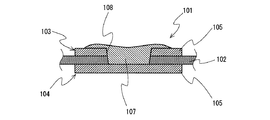
- the flexible printed wiring board 101 has conductive patterns 103 and 104 laminated on the front and back surfaces of the substrate 102, and the conductive patterns 103 and 104 have circular lands 105 having the same diameter at the opposing positions. is doing.
- a blind via hole 108 is formed in the substrate 102 and the land portion 105 on the front surface side.
- the blind via hole 108 is filled with a conductive paste by printing, and the conductive paste is cured to form a blind via hole 107, and the land portions 105 on the front and back surfaces are made conductive (Japanese Patent Laid-Open No. 62). -120096).
- the land portion 105 is wider than the other portions of the normal circuit pattern and the capacitor capacity of the land portion 105 is large, the land portion 105 may cause impedance mismatch.
- the present invention has been made in view of the above inconveniences, and the formation of blind via holes can be easily and reliably performed. Moreover, the present invention can accurately cope with a narrow pitch land of a mounted component, and further has an impedance. It is an object of the present invention to provide a double-sided printed wiring board and a method for manufacturing the same, which can effectively suppress the mismatching.
- the double-sided printed wiring board according to the present invention made to solve the above problems is An insulating substrate, A first conductive pattern laminated on one surface of the substrate and having a first land portion; A double-sided printed wiring board comprising: a second conductive pattern having a second land portion opposed to the first land portion, and a blind via hole penetrating the first land portion and the substrate; , The average diameter of the outer shape of the first land portion is larger than the average diameter of the outer shape of the second land portion.
- the average diameter of the outer shape of the first land portion is larger than the average diameter of the outer shape of the second land portion, a blind via hole can be easily and reliably formed.
- the conductive paste is printed on the blind via hole by printing and the blind via hole is formed by curing the conductive paste, the conductive paste is printed by the relatively wide first land portion. The position error can be accurately absorbed, and the conductive paste can be filled easily and reliably in the blind via hole. For this reason, the conductor is easily and reliably formed.
- the second land portions are easily provided at a narrow pitch. For this reason, for example, it is possible to cope with the case where the lands are arranged at a narrow pitch like a flip chip, and even in that case, the above-described decrease in the ease of forming the blind via hole can be effectively suppressed. Further, since the outer shape of the second land portion is reduced, the capacitor capacity of the second land portion is smaller than that of the conventional one, and impedance mismatching can be effectively suppressed.
- the double-sided printed wiring board can adopt a configuration in which the outer shape of the blind via hole, the first land portion, and the second land portion is formed in a substantially circular shape. Thereby, it is easy to reliably form even a small blind via hole.
- the first land portion is disposed substantially concentrically with the blind via hole.
- the first land portion disposed substantially concentrically with the blind via hole can reliably absorb the error in the planar direction when the conductor is formed, and the conductor can be formed more accurately.
- the second land portion is disposed substantially concentrically with the blind via hole. As a result, the second land portion and the substrate are joined with equal strength in the circumferential direction.
- the average diameter of the outer shape of the second land portion is not more than 5/6 times the average diameter of the outer shape of the first land portion. Accordingly, it is easy to dispose the second land portions at a narrow pitch, and errors in the planar direction when forming the blind via hole can be reliably absorbed by the first land portions.
- the average diameter of the outer shape of the first land portion is preferably at least twice the average diameter of the outer shape of the blind via hole. As a result, the first land portion can reliably absorb errors in the planar direction when the conductor is formed.
- the average diameter of the outer shape of the second land portion is preferably not more than four times the average diameter of the blind via hole. Thereby, it becomes easy to arrange the second land portions at a narrow pitch.
- the substrate is preferably flexible in the double-sided printed wiring board.
- the said double-sided printed wiring board can be utilized as a flexible printed wiring board.
- the blind via hole may be formed by curing a conductive paste containing conductive particles. Thereby, the conductive paste is filled in the hole for the blind via hole by printing, and the conductive paste is cured, whereby the conductor constituting the blind via hole can be easily and reliably formed.
- the blind via hole preferably has a combination of flat spherical conductive particles. Thereby, the electrical conduction state between the second land portion and the first land portion is reliably maintained by the combination of conductive particles.
- the method for producing a double-sided printed wiring board according to the present invention which has been made to solve the above problems, Forming a first conductive pattern having a first land portion on one surface of an insulating substrate; Forming a second conductive pattern having a second land portion opposed to the first land portion on the other surface of the substrate; A method for manufacturing a double-sided printed wiring board, comprising: forming a blind via hole hole penetrating the first land portion and a substrate; and printing a conductive paste containing conductive particles in the blind via hole hole. , The average diameter of the outer shape of the first land portion is larger than the average diameter of the outer shape of the second land portion.
- the method for manufacturing a double-sided printed wiring board can provide the double-sided printed wiring board having the above-described configuration, and thus has the advantages described above. That is, according to the method for manufacturing the double-sided printed wiring board, the average diameter of the outer shape of the first land portion is larger than the average diameter of the outer shape of the second land portion. The error can be accurately absorbed and the blind via hole can be formed easily and reliably. Moreover, since the average diameter of the external shape of the second land portion is smaller than the average diameter of the external shape of the first land portion, the method for manufacturing the double-sided printed wiring board can provide the second land portions at a narrow pitch. Therefore, for example, a double-sided printed wiring board in which lands are arranged at a narrow pitch like a flip chip can be manufactured. Furthermore, according to the manufacturing method of the double-sided printed wiring board, since the second land portion can be provided small, the capacitor capacity of the second land portion is small, and impedance mismatch can be effectively suppressed.
- outer shape means the maximum outer shape in a planar projection shape parallel to the substrate.
- Average diameter means an average value of the maximum width of the outer shape and the width of the outer shape in the direction orthogonal to the maximum width direction.
- Outer shape of blind via hole means the outer shape of a conductor in a hole for a blind via hole penetrating the first land portion and the substrate, and overflows from the hole for the blind via hole and is laminated on the surface of the first land portion. The shape of the conductor is not included.
- substantially circular 85% or more of the outer edge is an arc, and the ratio of the average distance (average radius) from the center of the arc to the radius at each arc-shaped point is 85% or more and 115% or less. Means that. Furthermore, “substantially concentric” means that the distance between the centers of the circles is 1/10 or less of the diameter of the larger circle.
- the double-sided printed wiring board and the manufacturing method thereof can easily and reliably form a blind via hole, and can appropriately cope with a land having a narrow pitch, and further effectively suppress impedance mismatching.
- a double-sided printed wiring board can be obtained.
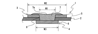
- FIG. 1 is an explanatory diagram of a double-sided printed wiring board according to an embodiment of the present invention, and is a schematic end view perpendicular to a substrate.
- FIG. 2 is a schematic end view for explaining the method of manufacturing the double-sided printed wiring board of FIG. 1, wherein A is a state before forming the first conductive pattern and the second conductive pattern, B is the first conductive pattern and The state after the formation of the second conductive pattern, C indicates a state in which a blind via hole is formed in the substrate, and D indicates a state in which a blind via hole is formed.
- FIG. 3 is an explanatory view of a conventional double-sided printed wiring board, and is a schematic end view perpendicular to the substrate.
- a flexible printed wiring board 1 of FIG. 1 includes an insulating substrate 2, a first conductive pattern 3 laminated on one surface of the substrate 2 (hereinafter sometimes referred to as a “printing surface”), and the substrate 2
- the second conductive pattern 4 is provided on the other surface (hereinafter also referred to as “mounting surface”).
- the first conductive pattern 3 has a plurality of first land portions 5, and the second conductive pattern 4 has a plurality of second land portions 6 that face the first land portions 5.
- the flexible printed wiring board 1 includes a plurality of blind via holes 7 that penetrate the first land portion 5 and the substrate 2.
- substrate 2 is comprised from the sheet-like member which has flexibility, and can specifically employ
- a material for the resin film for example, polyimide, polyethylene terephthalate, or the like can be preferably used.
- the average thickness of the substrate 2 is not particularly limited, but is preferably 5 ⁇ m or more and 100 ⁇ m or less, and more preferably 10 ⁇ m or more and 50 ⁇ m or less. If the average thickness of the substrate 2 is less than the lower limit, the strength of the substrate 2 may be insufficient. Further, if the average thickness of the substrate 2 exceeds the above upper limit, it may be against the demand for thinning.
- the first conductive pattern 3 is formed in a desired planar shape (pattern) by etching a metal layer laminated on the printing surface of the substrate 2.
- the first conductive pattern 3 can be formed of a conductive material, but is generally formed of copper, for example.
- the average thickness of the first conductive pattern 3 is not particularly limited, but is preferably 2 ⁇ m or more and 30 ⁇ m or less, and more preferably 5 ⁇ m or more and 20 ⁇ m or less. There exists a possibility that electroconductivity may become inadequate that the average thickness of the 1st conductive pattern 3 is less than the said minimum. Moreover, when the average thickness of the 1st conductive pattern 3 exceeds the said upper limit, there exists a possibility that a flexibility may be impaired.
- the first land portion 5 of the first conductive pattern 3 has a substantially circular outer shape (outer peripheral edge). Further, the first land portion 5 has a blind via hole 8 having a circular shape in a plan view at the center, and is provided in an annular shape in a plan view as a whole. The outer peripheral edge and the inner peripheral edge of the first land portion 5 are formed concentrically.
- the substrate 2 is also provided with blind via hole holes at positions corresponding to the blind via hole 8 of the first land portion 5.
- the outer diameter W2 of the first land portion 5 (average outer diameter) and the outer diameter W1 of the blind via hole 8 (average outer diameter of the blind via hole 7) will be described later.
- the second conductive pattern 4 is formed in a desired planar shape (pattern) by etching a metal layer laminated on the back surface of the substrate 2. Similar to the first conductive pattern 3, the second conductive pattern 4 is formed of copper, for example.
- the average thickness of the second conductive pattern 4 is not particularly limited, but is preferably 2 ⁇ m or more and 30 ⁇ m or less, and more preferably 5 ⁇ m or more and 20 ⁇ m or less. There exists a possibility that electroconductivity may become inadequate that the average thickness of the 2nd conductive pattern 4 is less than the said minimum. Moreover, when the average thickness of the 2nd conductive pattern 4 exceeds the said upper limit, there exists a possibility that a flexibility may be impaired.
- the second land portion 6 of the second conductive pattern 4 has a larger outer diameter than the blind via hole 8 and is disposed so as to close the opening on the mounting surface side of the blind via hole 8.
- the second land portion 6 has a substantially circular outer shape. Specifically, the second land portion 6 is disposed concentrically with the first land portion 5 and the blind via hole 8.
- outer diameter W3 (average outer diameter) of the second land portion 6 will be described later.
- the blind via hole 7 is intended to electrically connect the first land portion 5 and the second land portion 6, and has a conductor filled in the blind via hole 8.
- the blind via hole 7 is formed by curing after a conductive paste containing conductive particles is supplied into the blind via hole 8. Specifically, the conductive paste is supplied into the blind via hole 8 by printing from the printing surface side. For this reason, the bottom portion of the blind via hole 7 is in contact with the second land portion 6. The conductive paste overflows from the blind via hole 8 and covers a part of the first land portion 5.
- the blind via hole 7 is formed by curing after a certain time has elapsed after the conductive paste is supplied. Since the conductive paste flows between the supply and the curing, the blind via hole 7 has a recess 7a near the center.
- the conductive paste contains conductive particles and a binder resin thereof.
- Metal particles are preferably used as the conductive particles, and silver, copper, nickel and the like are preferably used as the material of the metal particles.
- the conductive paste preferably includes conductive particles having a flat spherical shape (a shape obtained by flattening a sphere), whereby the conductive particles and the conductive particles easily contact the second land portion 6 or the first land portion 5.
- Excellent conductivity In the flat spherical shape, the length of the short axis is preferably 0.2 times or more and less than 1 time of the length of the long axis in the cross section including the short axis and the long axis. More preferably, it is less than 8 times. When the ratio of the length between the minor axis and the major axis is in the above range, a conductor having excellent conductivity can be obtained.
- the flat conductive particles those having an average particle diameter (average value of length of major axis) of 0.5 ⁇ m or more and 3 ⁇ m or less are preferably used. When the average particle diameter is in the above range, a conductor having excellent conductivity can be obtained.
- the conductive paste can also include a plurality of types of conductive particles having different average particle diameters.
- the conductive paste is heated and cured.
- the conductive paste is heated at a temperature at which the conductive particles are bonded to each other.
- the conductive particles are bonded (melt bonded or sintered bonded) at the contact portion. That is, the conductor has a combination of conductive particles. Note that there may be some conductive particles that are not bonded as described above.
- binder resin epoxy resin, phenol resin, polyester resin, acrylic resin, melamine resin, polyimide resin, polyamideimide resin, phenoxy resin, and the like can be used.
- a thermosetting resin is preferably used.
- the kind of epoxy resin is not particularly limited, for example, a bisphenol type epoxy resin made from bisphenol A, bisphenol S, bisphenol AD, or the like can be used. Further, naphthalene type epoxy resin, novolac type epoxy resin, biphenyl type epoxy resin, dicyclopentadiene type epoxy resin, or the like can be used. Moreover, it is possible to use either a one-component epoxy resin or a two-component epoxy resin. Further, as the resin binder, it is also possible to use a one-component epoxy resin in which a microcapsule type curing agent is dispersed in an epoxy resin. In the conductive paste, butyl carbitol acetate or ethyl carbitol acetate can be used as a solvent in order to uniformly disperse the microcapsule type curing agent.
- the average outer diameter (outer diameter W1) of the blind via hole 7 is not particularly limited, but is preferably 20 ⁇ m or more and 150 ⁇ m or less, more preferably 30 ⁇ m or more and 120 ⁇ m or less, and 40 ⁇ m or more and 100 ⁇ m or less. More preferably it is. If the outer diameter W1 of the blind via hole 7 is less than the lower limit, it may be difficult to fill the conductor. On the other hand, if the outer diameter W1 of the blind via hole 7 exceeds the upper limit, the blind via hole 7 becomes large and the second land portion 6 described later may become too large.
- the outer shape of the blind via hole 7 means the outer shape of the conductive paste that does not include the conductive paste that overflows from the blind via hole 8 and covers the first land portion 5 and is hardened in the blind via hole 8.
- the plurality of blind via holes 7 are arranged in a constant arrangement in a plan view, for example, arranged in a lattice pattern at a constant pitch in one direction and another direction in a plan view.
- the arrangement pitch of the blind via holes 7 is not particularly limited, but may be 100 ⁇ m or more and 500 ⁇ m or less.
- the first land portion 5 has an inner diameter that is substantially the same as the outer diameter of the blind via hole 8 and an outer diameter W2 (an average diameter of the outer shape) that is larger than the outer diameter W3 of the second land portion 6.
- the outer diameter W2 of the first land portion 5 preferably has the following relationship with the outer diameter W1 of the blind via hole 7. That is, the outer diameter W2 of the first land portion 5 is preferably at least twice as large as the outer diameter W1 of the blind via hole 7, more preferably at least 2.3 times, and more than 2.5 times. Is more preferable. Thereby, the printing yield of the conductive paste can be improved.
- the outer diameter W2 of the first land portion 5 is preferably not more than 6 times the outer diameter W1 of the blind via hole 7, more preferably not more than 5.5 times, and further preferably not more than 5 times. preferable. If the outer diameter W2 of the first land portion 5 exceeds the above upper limit, the first land portion 5 becomes unnecessarily too large, and the design of the first conductive pattern 3 may be difficult.
- the radial width of the first land portion 5 (the width between the inner peripheral edge and the outer peripheral edge ((W2-W1) / 2)) is preferably 40 ⁇ m or more and 150 ⁇ m or less, and 45 ⁇ m or more and 125 ⁇ m or less. Is more preferable. If the width in the radial direction of the first land portion 5 is less than the lower limit, the printing yield of the conductive paste may not be improved. In addition, if the radial width of the first land portion 5 exceeds the upper limit, the design of the first conductive pattern 3 may be difficult.
- the outer diameter W2 of the first land portion 5 is preferably 100 ⁇ m or more and 400 ⁇ m or less, more preferably 130 ⁇ m or more and 380 ⁇ m or less, and further preferably 150 ⁇ m or more and 350 ⁇ m or less. If the outer diameter W2 of the first land portion 5 is less than the above lower limit, the printing yield of the conductive paste may be reduced. Further, if the outer diameter W2 of the first land portion 5 exceeds the upper limit, the design of the first conductive pattern 3 may be difficult.
- the outer diameter W3 (average outer diameter) of the second land portion 6 is preferably not more than 4 times the outer diameter W1 of the blind via hole 7, and more preferably not more than 3 times. If the outer diameter W3 of the second land portion 6 exceeds the upper limit, it may be difficult to dispose the second land portion 6 at a narrow pitch, and impedance mismatching can be effectively suppressed. It may not be possible. On the other hand, the outer diameter W3 of the second land portion 6 is preferably 1.2 times or more, and more preferably 1.5 times or more the outer diameter W1 of the blind via hole 7.
- the outer diameter W3 of the second land portion 6 is less than the above lower limit, the adhesion between the second conductive pattern 4 and the substrate 2 in the second land portion 6 and the electrical connection between the second land portion 6 and the blind via hole 7 are achieved. May be insufficient.
- the outer diameter W3 of the second land portion 6 is preferably 5/6 or less of the outer diameter W2 of the first land portion 5, and more preferably 5/7 or less.
- the outer diameter W3 of the second land portion 6 is preferably not less than 1/6 of the outer diameter W2 of the first land portion 5, and more preferably not less than 1/3.
- the outer diameter W3 of the second land portion 6 is preferably 50 ⁇ m or more and 300 ⁇ m or less, more preferably 70 ⁇ m or more and 280 ⁇ m or less, and further preferably 90 ⁇ m or more and 250 ⁇ m or less. If the outer diameter W3 of the second land portion 6 is less than the lower limit, the adhesive force between the second conductive pattern 4 and the substrate 2 in the second land portion 6 may be insufficient. If the outer diameter W3 of the second land portion 6 exceeds the upper limit, it is difficult to dispose the second land portion 6 at a narrow pitch, and impedance mismatching may not be effectively suppressed.
- the area of the first land portion 5 (the area in an annular plan view excluding the opening area of the blind via hole 8) is at least four times the area of the blind via hole 7 (the opening area of the blind via hole 8). It is preferably less than or equal to double, and more preferably between 5 and 25 times. As a result, the printing yield of the conductive paste can be improved and the design of the first conductive pattern 3 can be facilitated.
- the area of the first land portion 5 (the area in an annular plan view excluding the opening area of the blind via hole 8) is not less than 1.3 times and not more than 5 times the area of the second land portion 6. Is more preferable, and it is more preferably 1.8 times or more and 4 times or less. As a result, it is possible to achieve both improvement in the printing yield of the conductive paste and narrowing of the pitch of the second land portions 6, and it is possible to effectively suppress impedance mismatching.
- the area of the second land portion 6 (area in plan view) is preferably 2.5 to 20 times the area of the blind via hole 7 (opening area of the blind via hole 8), preferably 2.7. It is more preferable that it is not less than twice and not more than 7 times. If the area of the second land portion 6 is less than the lower limit, the adhesive force between the second conductive pattern 4 and the substrate 2 in the second land portion 6 may be insufficient. If the area of the second land portion 6 exceeds the upper limit, it is difficult to dispose the second land portion 6 at a narrow pitch, and impedance mismatching may not be effectively suppressed.
- the manufacturing method of the flexible printed wiring board 1 includes a first conductive pattern forming step of forming a first conductive pattern 3 having a first land portion 5 on the printed surface of the substrate 2, and a first land portion on the mounting surface of the substrate 2.
- the second conductive pattern forming step for forming the second conductive pattern 4 having the second land portion 6 facing the substrate 5 and the blind via hole 8 penetrating the first land portion 5 and the substrate 2 are formed as shown in FIG.
- first conductive pattern forming step and second conductive pattern forming step In the first conductive pattern forming step and the second conductive pattern forming step, the first conductive pattern 3 and the second conductive pattern 4 are formed on each surface of the substrate 2 (see B in FIG. 2). Here, the second land portion 6 of the second conductive pattern 4 and the first land portion 5 of the first conductive pattern 3 are formed at positions facing each other.
- description here is abbreviate
- the 2nd conductive pattern 4 and the 1st conductive pattern 3 can be formed by a conventionally well-known method, for example, etches the desired location of the metal layer laminated
- a blind via hole 8 is formed in the substrate 2 by irradiating the center of the annular first land portion 5 with a laser beam. Further, the residue is removed by desmearing after the laser beam irradiation.
- the blind via hole forming step includes a step of preparing a conductive paste containing conductive particles, a step of printing the conductive paste in the blind via hole 8, and a step of leaving the printed conductive paste for a certain period of time to flow. And a step of heating and hardening the conductive paste after flowing.
- the conductive paste may be prepared so that the thixotropy index of the conductive paste is preferably 0.40 or less, more preferably 0.25 or less.
- the thixotropy index is a value calculated by the following formula (1).
- Thixotropic index log ( ⁇ 1 / ⁇ 2) / log (D2 / D1) (1)
- D1 and D2 mean shear rates, and
- ⁇ 1 means the viscosity of the conductive paste at the shear rate D1
- ⁇ 2 means the viscosity of the conductive paste at the shear rate D2.
- ⁇ 1 is preferably 20 Pa ⁇ s or more and 300 Pa ⁇ s or less, and more preferably 40 Pa ⁇ s or more and 150 Pa ⁇ s or less.
- ⁇ 1 is in the above range, the conductive paste can be easily and surely printed on the blind via hole 8 and a suitable blind via hole 7 can be formed.
- a conventionally known method can be adopted, for example, a screen printing method or an ink jet printing method can be adopted.
- the outer diameter of the first land portion 5 on the printed surface is larger than the outer diameter of the second land portion 6 on the mounting surface.
- the first land portion 5 is evenly arranged on the outer periphery of the opening of the blind via hole 8.
- the first land portion 5 can absorb the error in the printing position and further improve the printing yield.
- the flexible printed wiring board 1 has the second land portion 6 having an outer diameter smaller than the outer diameter of the first land portion 5, the second land portions 6 can be provided at a narrow pitch, and therefore, the flip chip.
- a land having a narrow pitch as shown above can also be suitably handled.
- the capacitor capacity of the second land portion 6 is smaller than that of the conventional one, so that impedance mismatch can be effectively suppressed.
- the land portions of the respective surfaces have the same diameter as in the conventional case, and the flexible printed wiring board 1 in the vicinity of the first land portion 5 and the second land portion 6 is used. Rich in flexibility.
- a flexible printed wiring board has been described as an example of a double-sided printed wiring board, but the scope of the present invention is not limited to this.
- a rigid printed wiring board can also be adopted.
- the double-sided printed wiring board can also be employed in a rigid flexible printed wiring board in which a flexible printed wiring board and a rigid printed wiring board are integrated, a build-up board having a multilayer structure, or the like.
- the relationship between the outer diameter of the first land portion 5 and the outer diameter of the second land portion 6 is not necessarily limited to that within the numerical range shown in the above embodiment. If the average diameter of the outer shape is smaller than the average diameter of the outer shape of the first land portion 5, it is within the scope of the present invention.
- the blind via hole 7, the second land portion 6, and the first land portion 5 have been described as having substantially circular outer shapes.
- the blind via hole 7, the second land portion 6, and the first land 5 have been described.
- the shape of the outer shape of the part 5 is not particularly limited.
- the outer shape of the blind via hole 7 and the outer shape of the first land portion 5 are similar to each other, but the present invention is not limited to this.
- the outer shape of the blind via hole 7 and the outer shape of the first land portion 5 are similar to each other as in the above embodiment, so that the width of the first land portion 5 (the radial width in the case of a circle) is constant. Therefore, there is an advantage that the blind via hole 7 can be formed with high accuracy.
- the present invention can be suitably used for a flexible printed wiring board, for example.
Landscapes
- Engineering & Computer Science (AREA)
- Microelectronics & Electronic Packaging (AREA)
- Manufacturing & Machinery (AREA)
- Printing Elements For Providing Electric Connections Between Printed Circuits (AREA)
Description
本発明は、両面プリント配線板及びその製造方法に関する。
両面プリント配線板としては、可撓性基板の表裏面に導電パターンを配設したフレキシブルプリント配線板や、硬質基板を用いたリジッドプリント配線板や、硬質基板と可撓性基板とを積層したリジッドフレキシブルプリント配線板等が公知である。上記フレキシブルプリント配線板101は、図3に示すように、基板102の表裏面に導電パターン103,104が積層され、この導電パターン103,104が同径の円形のランド部105を対向位置に有している。この基板102及び表面側のランド部105にブラインドビアホール用孔108が形成されている。そして、このブラインドビアホール用孔108に導電性ペーストを印刷によって満たし、この導電性ペーストを硬化することで、ブラインドビアホール107が形成され、表裏面のランド部105を導通させている(特開昭62-120096号公報参照)。
このような従来のフレキシブルプリント配線板101等の両面プリント配線板にあっては、例えばフリップチップのように実装部品のランドが狭ピッチである場合、ランド部105が配置できないおそれがある。かかる観点から実装部品の狭ピッチのランドに対応するようにフレキシブルプリント配線板のランド部105を小さく設けることも考えられる。しかしランド部105を小さくした場合には、ブラインドビアホール107を形成する際に導電性ペーストをブラインドビアホール用孔に的確に印刷して満たすことができず、印刷歩留りが低下するおそれがある。
また、ランド部105は通常回路パターンの他の部分よりも幅が広く、ランド部105のコンデンサ容量が大きいため、ランド部105によってインピーダンスの不整合が生ずるおそれがある。
本発明は、上記のような不都合に鑑みてなされたものであり、ブラインドビアホールの形成が容易且つ確実に行われ、しかも実装部品の狭ピッチのランドにも的確に対応することができ、さらにインピーダンスの不整合を効果的に抑制できる両面プリント配線板及びその製造方法を提供することを目的とする。
上記課題を解決するためになされた本発明に係る両面プリント配線板は、
絶縁性を有する基板、
この基板の一方の面に積層され、第1ランド部を有する第1導電パターン、
基板の他方の面に積層され、上記第1ランド部に対向する第2ランド部を有する第2導電パターン、及び
第1ランド部と基板とを貫通するブラインドビアホール
を備える両面プリント配線板であって、
上記第1ランド部の外形の平均径が第2ランド部の外形の平均径よりも大きいことを特徴とする。
絶縁性を有する基板、
この基板の一方の面に積層され、第1ランド部を有する第1導電パターン、
基板の他方の面に積層され、上記第1ランド部に対向する第2ランド部を有する第2導電パターン、及び
第1ランド部と基板とを貫通するブラインドビアホール
を備える両面プリント配線板であって、
上記第1ランド部の外形の平均径が第2ランド部の外形の平均径よりも大きいことを特徴とする。
当該両面プリント配線板は、第1ランド部の外形の平均径が第2ランド部の外形の平均径よりも大きいので、ブラインドビアホールを容易且つ確実に形成することができる。つまり、例えば印刷によって導電性ペーストをブラインドビアホール用孔に印刷し、この導電性ペーストを硬化することでブラインドビアホールを形成する場合にあっては、比較的広い第1ランド部によって導電性ペーストの印刷位置の誤差を的確に吸収し、ブラインドビアホール用孔に容易且つ確実に導電性ペーストを満たすことができる。このため導電体が容易且つ確実に形成される。
また、第1ランド部の外形の平均径よりも第2ランド部の外形の平均径が小さいので、第2ランド部を狭ピッチに設けやすい。このため例えばフリップチップのようにランドが狭ピッチで配設される場合にも対応でき、かつその場合でも上述のブラインドビアホール形成容易性の低下を効果的に抑制できる。また、第2ランド部の外形を小さくしているため、この第2ランド部のコンデンサ容量が従来のものに比べて小さく、インピーダンスの不整合を効果的に抑制することができる。
当該両面プリント配線板は、ブラインドビアホール、第1ランド部及び第2ランド部の外形が略円形に形成されている構成を採用可能である。これにより、小さなブラインドビアホール等であっても確実に形成しやすい。
上記ブラインドビアホールと略同心状に第1ランド部が配設されていることが好ましい。これによりブラインドビアホールと略同心状に配設された第1ランド部によって導電体形成時の平面方向の誤差を確実に吸収することができ、より的確に導電体を形成することができる。また、ブラインドビアホールと略同心状に第2ランド部が配設されていることが好ましい。これにより第2ランド部と基板とが周方向に均等な強度で接合されることになる。
第2ランド部の外形の平均径は、第1ランド部の外形の平均径の5/6倍以下であることが好ましい。これにより、第2ランド部を狭ピッチに配設することが容易であり、また第1ランド部によってブラインドビアホール形成時の平面方向の誤差を確実に吸収することができる。
第1ランド部の外形の平均径が、上記ブラインドビアホールの外形の平均径の2倍以上であることが好ましい。これにより、第1ランド部によって導電体形成時の平面方向の誤差を確実に吸収することができる。
第2ランド部の外形の平均径は、ブラインドビアホールの外形の平均径の4倍以下であることが好ましい。これにより、第2ランド部を狭ピッチに配設することが容易となる。
当該両面プリント配線板は、基板が可撓性を有することが好ましい。これにより当該両面プリント配線板をフレキシブルプリント配線板として利用することができる。
ブラインドビアホールは、導電粒子を含む導電性ペーストを硬化することで形成されているとよい。これにより導電性ペーストを印刷によってブラインドビアホール用孔に満たし、この導電性ペーストを硬化することで、ブラインドビアホールを構成する導電体を容易且つ確実に形成することができる。
ブラインドビアホールは、扁平球状の導電粒子の結合体を有することが好ましい。これにより第2ランド部と第1ランド部との電気的導通状態が導電粒子の結合体によって確実に維持される。
また、上記課題を解決すべくなされた本発明に係る両面プリント配線板の製造方法は、
絶縁性を有する基板の一方の面に、第1ランド部を有する第1導電パターンを形成する工程、
上記基板の他方の面に、第1ランド部に対向する第2ランド部を有する第2導電パターンを形成する工程、
上記第1ランド部と基板とを貫通するブラインドビアホール用孔を形成する工程、及び
上記ブラインドビアホール用孔に導電粒子を含む導電性ペーストを印刷する工程
を有する両面プリント配線板の製造方法であって、
上記第1ランド部の外形の平均径が第2ランド部の外形の平均径よりも大きいことを特徴とする。
絶縁性を有する基板の一方の面に、第1ランド部を有する第1導電パターンを形成する工程、
上記基板の他方の面に、第1ランド部に対向する第2ランド部を有する第2導電パターンを形成する工程、
上記第1ランド部と基板とを貫通するブラインドビアホール用孔を形成する工程、及び
上記ブラインドビアホール用孔に導電粒子を含む導電性ペーストを印刷する工程
を有する両面プリント配線板の製造方法であって、
上記第1ランド部の外形の平均径が第2ランド部の外形の平均径よりも大きいことを特徴とする。
当該両面プリント配線板の製造方法は、上述の構成からなる当該両面プリント配線板を形成することができるので、既述の利点を奏する。つまり、当該両面プリント配線板の製造方法によれば、第2ランド部の外形の平均径よりも第1ランド部の外形の平均径が大きいので、第1ランド部によって導電性ペーストの印刷位置の誤差を的確に吸収し、ブラインドビアホールを容易且つ確実に形成することができる。また、当該両面プリント配線板の製造方法は、第1ランド部の外形の平均径よりも第2ランド部の外形の平均径が小さいので、第2ランド部を狭ピッチに設けることができ、このため例えばフリップチップのようにランドが狭ピッチで配設されている両面プリント配線板を製造することができる。さらに、当該両面プリント配線板の製造方法によれば、第2ランド部が小さく設けることができるので、第2ランド部のコンデンサ容量が小さく、インピーダンスの不整合を効果的に抑制することができる。
なお、「外形」とは、基板と平行な平面投影形状で最大の外形を意味する。「平均径」とは、外形の最大幅と、その最大幅方向に直交方向の外形の幅との平均値を意味する。「ブラインドビアホールの外形」とは、第1ランド部及び基板を貫通するブラインドビアホール用孔内にある導電体の外形を意味し、このブラインドビアホール用孔から溢れ第1ランド部の表面に積層される導電体の形状は含まない。「略円形」とは、外縁の85%以上が円弧であり、その円弧の中心からの平均距離(平均半径)と、円弧状の各点における半径との比が85%以上115%以内であることを意味する。さらに、「略同心状」であるとは、円の中心同士の距離が大きい方の円の直径の1/10以下の距離にあることを意味する。
当該両面プリント配線板及びその製造方法は、ブラインドビアホールの形成が容易且つ確実に行われ、しかも狭ピッチのランドにも的確に対応することかでき、さらにはインピーダンスの不整合を効果的に抑制することができる両面プリント配線板を得ることができる。
1 フレキシブルプリント配線板
2 基板
3 第1導電パターン
4 第2導電パターン
5 第1ランド部
6 第2ランド部
7 ブラインドビアホール
8 ブラインドビアホール用孔
2 基板
3 第1導電パターン
4 第2導電パターン
5 第1ランド部
6 第2ランド部
7 ブラインドビアホール
8 ブラインドビアホール用孔
以下、本発明の実施形態について説明する。まず本発明に係る両面プリント配線板の一実施の形態としてフレキシブルプリント配線板について図1を参酌しつつ説明する。
[フレキシブルプリント配線板]
図1のフレキシブルプリント配線板1は、絶縁性を有する基板2、この基板2の一方の面(以下、「印刷面」ということがある)に積層される第1導電パターン3、及び基板2の他方の面(以下、「実装面」ということがある)に積層される第2導電パターン4を備えている。第1導電パターン3は複数の第1ランド部5を有し、第2導電パターン4は第1ランド部5に対向する複数の第2ランド部6を有している。また、フレキシブルプリント配線板1は、第1ランド部5及び基板2を貫通する複数のブラインドビアホール7を備えている。
図1のフレキシブルプリント配線板1は、絶縁性を有する基板2、この基板2の一方の面(以下、「印刷面」ということがある)に積層される第1導電パターン3、及び基板2の他方の面(以下、「実装面」ということがある)に積層される第2導電パターン4を備えている。第1導電パターン3は複数の第1ランド部5を有し、第2導電パターン4は第1ランド部5に対向する複数の第2ランド部6を有している。また、フレキシブルプリント配線板1は、第1ランド部5及び基板2を貫通する複数のブラインドビアホール7を備えている。
(基板)
基板2は、可撓性を有するシート状部材から構成されており、基板2としては具体的には樹脂フィルムを採用可能である。この樹脂フィルムの材料としては、例えばポリイミド、ポリエチレンテレフタレートなどが好適に採用可能である。
基板2は、可撓性を有するシート状部材から構成されており、基板2としては具体的には樹脂フィルムを採用可能である。この樹脂フィルムの材料としては、例えばポリイミド、ポリエチレンテレフタレートなどが好適に採用可能である。
基板2の平均厚みは、特に限定されるものではないが、5μm以上100μm以下であることが好ましく、10μm以上50μm以下であることがより好ましい。基板2の平均厚みが上記下限未満であると基板2の強度が不十分となるおそれがある。また基板2の平均厚みが上記上限を超えると薄型化の要請に反するおそれがある。
(第1導電パターン)
第1導電パターン3は、基板2の印刷面に積層された金属層をエッチングすることによって所望の平面形状(パターン)に形成されている。第1導電パターン3は、導電性を有する材料で形成可能であるが、一般的には例えば銅によって形成される。この第1導電パターン3の平均厚みは、特に限定されるものではないが、2μm以上30μm以下であることが好ましく、5μm以上20μm以下であることがより好ましい。第1導電パターン3の平均厚みが上記下限未満であると導通性が不十分となるおそれがある。また第1導電パターン3の平均厚みが上記上限を超えるとフレキシブル性を損なうおそれがある。
第1導電パターン3は、基板2の印刷面に積層された金属層をエッチングすることによって所望の平面形状(パターン)に形成されている。第1導電パターン3は、導電性を有する材料で形成可能であるが、一般的には例えば銅によって形成される。この第1導電パターン3の平均厚みは、特に限定されるものではないが、2μm以上30μm以下であることが好ましく、5μm以上20μm以下であることがより好ましい。第1導電パターン3の平均厚みが上記下限未満であると導通性が不十分となるおそれがある。また第1導電パターン3の平均厚みが上記上限を超えるとフレキシブル性を損なうおそれがある。
第1導電パターン3の第1ランド部5は、外形(外周縁)が略円形に設けられている。また第1ランド部5は、中央に平面視円形のブラインドビアホール用孔8を有しており、全体として平面視円環状に設けられている。第1ランド部5の外周縁及び内周縁は同心状に形成されている。なお、上記基板2にも、この第1ランド部5のブラインドビアホール用孔8に対応する位置にブラインドビアホール用孔が形成される。
なお、第1ランド部5の外径W2(外形の平均径)及びブラインドビアホール用孔8の外径W1(ブラインドビアホール7の外形の平均径)については後述する。
(第2導電パターン)
上記第2導電パターン4は、第1導電パターン3と同様に、基板2の裏面に積層された金属層をエッチングすることによって所望の平面形状(パターン)に形成されている。第2導電パターン4は上記第1導電パターン3と同様に例えば銅によって形成される。この第2導電パターン4の平均厚みは、特に限定されるものではないが、2μm以上30μm以下であることが好ましく、5μm以上20μm以下であることがより好ましい。第2導電パターン4の平均厚みが上記下限未満であると導通性が不十分となるおそれがある。また第2導電パターン4の平均厚みが上記上限を超えるとフレキシブル性を損なうおそれがある。
上記第2導電パターン4は、第1導電パターン3と同様に、基板2の裏面に積層された金属層をエッチングすることによって所望の平面形状(パターン)に形成されている。第2導電パターン4は上記第1導電パターン3と同様に例えば銅によって形成される。この第2導電パターン4の平均厚みは、特に限定されるものではないが、2μm以上30μm以下であることが好ましく、5μm以上20μm以下であることがより好ましい。第2導電パターン4の平均厚みが上記下限未満であると導通性が不十分となるおそれがある。また第2導電パターン4の平均厚みが上記上限を超えるとフレキシブル性を損なうおそれがある。
第2導電パターン4の第2ランド部6は、ブラインドビアホール用孔8よりも外径が大きくブラインドビアホール用孔8の実装面側の開口を閉塞するよう配設されている。第2ランド部6は、外形が略円形に設けられ、具体的には第1ランド部5及びブラインドビアホール用孔8と同心状に配設されている。
なお、第2ランド部6の外径W3(外形の平均径)については後述する。
(ブラインドビアホール)
ブラインドビアホール7は、第1ランド部5及び第2ランド部6の電気的導通を図るものであり、ブラインドビアホール用孔8に充填された導電体を有している。このブラインドビアホール7は、導電粒子を含む導電性ペーストがブラインドビアホール用孔8内に供給された後に硬化することで形成されている。具体的には、導電性ペーストは印刷面側から印刷によってブラインドビアホール用孔8内に供給される。このため、ブラインドビアホール7の底部が第2ランド部6と接している。また、導電性ペーストは、ブラインドビアホール用孔8から溢れ、第1ランド部5の一部を覆っている。
ブラインドビアホール7は、第1ランド部5及び第2ランド部6の電気的導通を図るものであり、ブラインドビアホール用孔8に充填された導電体を有している。このブラインドビアホール7は、導電粒子を含む導電性ペーストがブラインドビアホール用孔8内に供給された後に硬化することで形成されている。具体的には、導電性ペーストは印刷面側から印刷によってブラインドビアホール用孔8内に供給される。このため、ブラインドビアホール7の底部が第2ランド部6と接している。また、導電性ペーストは、ブラインドビアホール用孔8から溢れ、第1ランド部5の一部を覆っている。
また、ブラインドビアホール7は、導電性ペーストが供給された後一定時間経過後に硬化することで形成されている。供給後硬化するまでの間に導電性ペーストが流動するので、ブラインドビアホール7には、中心付近に凹み7aが形成されている。
上記導電性ペーストは、導電粒子とそのバインダ樹脂とを含んでいる。この導電粒子としては金属粒子が好適に用いられ、金属粒子の材料としては銀、銅、ニッケル等が好適に用いられる。
この導電性ペーストは、扁平球状(球を扁平させた形状)の導電粒子を含むことが好ましく、これによって導電粒子同士及び導電粒子と第2ランド部6又は第1ランド部5とが接触しやすく導電性に優れている。なお、扁平球状の形状は、短軸及び長軸を含む断面において短軸の長さが長軸の長さの0.2倍以上1倍未満であることが好ましく、0.4倍以上0.8倍未満であることがより好ましい。短軸と長軸との長さの比が上記範囲にあることによって導電性の優れた導電体を得ることができる。なお、この扁平形状の導電粒子は、平均粒子径(長軸の長さの平均値)が0.5μm以上3μm以下のものが好適に用いられる。平均粒子径が上記範囲にあることによって導電性の優れた導電体を得ることができる。なお、導電性ペーストは、平均粒子径の異なる複数種類の導電粒子を含むことも可能である。
また、ブラインドビアホール7の形成に際して、導電性ペーストを加熱して硬化している。ここで、導電性ペーストは、導電粒子同士が結合する程度の温度で加熱される。このため、導電粒子同士は接触部分で結合(溶融結合又は焼結結合)している。つまり、導電体は、導電粒子の結合体を有している。なお、上述のような結合していない導電粒子が一部に存在する場合もある。
上記バインダ樹脂としては、エポキシ樹脂、フェノール樹脂、ポリエステル樹脂、アクリル樹脂、メラミン樹脂、ポリイミド樹脂、ポリアミドイミド樹脂、フェノシキ樹脂等を用いることができる。なお、バインダ樹脂としては、熱硬化性樹脂が好適に用いられる。
エポキシ樹脂の種類は特に限定されないが、例えば、ビスフェノールA、ビスフェノールS、ビスフェノールAD等を原料とするビスフェノール型エポキシ樹脂を用いることができる。また、ナフタレン型エポキシ樹脂、ノボラック型エポキシ樹脂、ビフェニル型エポキシ樹脂、ジシクロペンタジエン型エポキシ樹脂等を用いることができる。また、一液性のエポキシ樹脂及び二液性のエポキシ樹脂の何れも用いることが可能である。また、樹脂バインダとしては、マイクロカプセル型の硬化剤をエポキシ樹脂に分散した一液性エポキシ樹脂を用いることも可能である。なお、導電性ペーストは、マイクロカプセル型の硬化剤を均一に分散させるために溶媒としてブチルカルビトールアセテートやエチルカルビトールアセテートを用いることが可能である。
(各部材の径等について)
ブラインドビアホール7の外形の平均径(外径W1)は、特に限定されるものではないが、20μm以上150μm以下であることが好ましく、30μm以上120μm以下であることがより好ましく、40μm以上100μm以下であることがさらに好ましい。ブラインドビアホール7の外径W1が上記下限未満であると、導電体を充填することが困難となるおそれがある。逆に、上記ブラインドビアホール7の外径W1が上記上限を超えると、ブラインドビアホール7が大きくなることで後述する第2ランド部6が大きくなり過ぎるおそれがある。なお、ブラインドビアホール7の外形とは、ブラインドビアホール用孔8から溢れて第1ランド部5を覆う導電性ペーストを含まず、ブラインドビアホール用孔8内で硬化した導電性ペーストの外形を意味する。
ブラインドビアホール7の外形の平均径(外径W1)は、特に限定されるものではないが、20μm以上150μm以下であることが好ましく、30μm以上120μm以下であることがより好ましく、40μm以上100μm以下であることがさらに好ましい。ブラインドビアホール7の外径W1が上記下限未満であると、導電体を充填することが困難となるおそれがある。逆に、上記ブラインドビアホール7の外径W1が上記上限を超えると、ブラインドビアホール7が大きくなることで後述する第2ランド部6が大きくなり過ぎるおそれがある。なお、ブラインドビアホール7の外形とは、ブラインドビアホール用孔8から溢れて第1ランド部5を覆う導電性ペーストを含まず、ブラインドビアホール用孔8内で硬化した導電性ペーストの外形を意味する。
複数のブラインドビアホール7は、平面視一定配列で配置されており、例えば平面視一方向及び他方向に一定ピッチで格子状に配置されている。ここで、ブラインドビアホール7の配設ピッチは特に限定されるものではないが、100μm以上500μm以下とすることができる。
第1ランド部5は、内径がブラインドビアホール用孔8の外径と略同一であり、外径W2(外形の平均径)が第2ランド部6の外径W3よりも大きい。また、第1ランド部5の外径W2は、ブラインドビアホール7の外径W1と以下の関係を有することが好ましい。つまり、第1ランド部5の外径W2は、ブラインドビアホール7の外径W1の2倍以上であることが好ましく、2.3倍以上であることがより好ましく、2.5倍以上であることがさらに好ましい。これにより、導電性ペーストの印刷歩留りの向上を図ることができる。一方、第1ランド部5の外径W2は、ブラインドビアホール7の外径W1の6倍以下であることが好ましく、5.5倍以下であることがより好ましく、5倍以下であることがさらに好ましい。第1ランド部5の外径W2が上記上限を超えると不必要に第1ランド部5が大きくなり過ぎ、第1導電パターン3の設計が困難となるおそれがある。
また、第1ランド部5の径方向の幅(内周縁と外周縁との幅((W2-W1)/2))は、40μm以上150μm以下であることが好ましく、45μm以上125μm以下であることがより好ましい。第1ランド部5の径方向の幅が上記下限未満であると、導電性ペーストの印刷歩留りの向上が図れないおそれがある。また第1ランド部5の径方向の幅が上記上限を超えると、第1導電パターン3の設計が困難となるおそれがある。
なお、第1ランド部5の外径W2は、具体的には、100μm以上400μm以下であることが好ましく、130μm以上380μm以下であることがより好ましく、150μm以上350μm以下であることがさらに好ましい。第1ランド部5の外径W2が上記下限未満であると、導電性ペーストの印刷歩留りが低下するおそれがある。また第1ランド部5の外径W2が上記上限を超えると、第1導電パターン3の設計が困難となるおそれがある。
第2ランド部6の外径W3(外形の平均径)は、ブラインドビアホール7の外径W1の4倍以下であることが好ましく、3倍以下であることがより好ましい。第2ランド部6の外径W3が上記上限を超えると、第2ランド部6を狭ピッチに配設することが困難となるおそれがあり、またインピーダンスの不整合を効果的に抑制することができないおそれがある。一方、第2ランド部6の外径W3は、ブラインドビアホール7の外径W1の1.2倍以上であることが好ましく、1.5倍以上であることがさらに好ましい。第2ランド部6の外径W3が上記下限未満であると、第2ランド部6における第2導電パターン4と基板2との接着力ひいては第2ランド部6とブラインドビアホール7との導通性が不十分となるおそれがある。
また、第2ランド部6の外径W3は、第1ランド部5の外径W2の5/6以下であることが好ましく、5/7以下であることがより好ましい。一方、第2ランド部6の外径W3は、第1ランド部5の外径W2の1/6以上であることが好ましく、1/3以上であることがより好ましい。第2ランド部6の外径W3と第1ランド部5の外径W2との比を上記範囲とすることによって、導電性ペーストの印刷歩留りの向上及び第2ランド部6の狭ピッチ化を図ることができ、さらにインピーダンスの不整合を効果的に抑制することができる。
なお、第2ランド部6の外径W3は、具体的には、50μm以上300μm以下であることが好ましく、70μm以上280μm以下であることがより好ましく、90μm以上250μm以下であることがさらに好ましい。第2ランド部6の外径W3が上記下限未満であると、第2ランド部6における第2導電パターン4と基板2との接着力が不十分となるおそれがある。また第2ランド部6の外径W3が上記上限を超えると、第2ランド部6を狭ピッチに配設することが困難となり、またインピーダンスの不整合を効果的に抑制できなくなるおそれがある。
また、第1ランド部5の面積(ブラインドビアホール用孔8の開口面積を除いた円環状の平面視の面積)はブラインドビアホール7の面積(ブラインドビアホール用孔8の開口面積)の4倍以上50倍以下であることが好ましく、5倍以上25倍以下であることがより好ましい。これにより、導電性ペーストの印刷歩留りの向上が図れるとともに第1導電パターン3の設計が容易となる。
また、第1ランド部5の面積(ブラインドビアホール用孔8の開口面積を除いた円環状の平面視の面積)は、第2ランド部6の面積の1.3倍以上5倍以下であることが好ましく、1.8倍以上4倍以下であることがより好ましい。これにより、導電性ペーストの印刷歩留りの向上と第2ランド部6の狭ピッチ化を両立することが可能となり、さらにはインピーダンスの不整合を効果的に抑制することができる。
また、第2ランド部6の面積(平面視の面積)は、ブラインドビアホール7の面積(ブラインドビアホール用孔8の開口面積)の2.5倍以上20倍以下であることが好ましく、2.7倍以上7倍以下であることがより好ましい。第2ランド部6の面積が上記下限未満であると、第2ランド部6における第2導電パターン4と基板2との接着力が不十分となるおそれがある。また第2ランド部6の面積が上記上限を超えると、第2ランド部6を狭ピッチに配設することが困難となり、またインピーダンスの不整合を効果的に抑制できなくなるおそれがある。
[フレキシブルプリント配線板の製造方法]
次に、上記フレキシブルプリント配線板1を製造する方法について図2を参酌しつつ説明する。当該フレキシブルプリント配線板1の製造方法は、基板2の印刷面に第1ランド部5を有する第1導電パターン3を形成する第1導電パターン形成工程と、基板2の実装面に第1ランド部5に対向する第2ランド部6を有する第2導電パターン4を形成する第2導電パターン形成工程と、上記第1ランド部5及び基板2を貫通するブラインドビアホール用孔8を図2のCのように形成するブランイドビアホール用孔形成工程と、上記ブラインドビアホール用孔8にブラインドビアホール7を図2のDのように形成するブラインドビアホール形成工程を有する。
次に、上記フレキシブルプリント配線板1を製造する方法について図2を参酌しつつ説明する。当該フレキシブルプリント配線板1の製造方法は、基板2の印刷面に第1ランド部5を有する第1導電パターン3を形成する第1導電パターン形成工程と、基板2の実装面に第1ランド部5に対向する第2ランド部6を有する第2導電パターン4を形成する第2導電パターン形成工程と、上記第1ランド部5及び基板2を貫通するブラインドビアホール用孔8を図2のCのように形成するブランイドビアホール用孔形成工程と、上記ブラインドビアホール用孔8にブラインドビアホール7を図2のDのように形成するブラインドビアホール形成工程を有する。
(第1導電パターン形成工程及び第2導電パターン形成工程)
第1導電パターン形成工程及び第2導電パターン形成工程においては、基板2の各面に第1導電パターン3及び第2導電パターン4を形成する(図2のB参照)。ここで、第2導電パターン4の第2ランド部6と第1導電パターン3の第1ランド部5とは対向する位置に形成される。なお、第2ランド部6及び第1ランド部5の形状等は上述のフレキシブルプリント配線板1で説明した通りであるのでここでの説明を省略する。なお、第2導電パターン4及び第1導電パターン3は従来公知の方法で形成することができ、例えば図2のAのように基板2の各面に積層された金属層の所望箇所をエッチングすることによって図2のBのように形成することができる。また、第1導電パターン形成工程と第2導電パターン形成工程とは、同時に行うことも可能であり、また別々に行うことも可能である。
第1導電パターン形成工程及び第2導電パターン形成工程においては、基板2の各面に第1導電パターン3及び第2導電パターン4を形成する(図2のB参照)。ここで、第2導電パターン4の第2ランド部6と第1導電パターン3の第1ランド部5とは対向する位置に形成される。なお、第2ランド部6及び第1ランド部5の形状等は上述のフレキシブルプリント配線板1で説明した通りであるのでここでの説明を省略する。なお、第2導電パターン4及び第1導電パターン3は従来公知の方法で形成することができ、例えば図2のAのように基板2の各面に積層された金属層の所望箇所をエッチングすることによって図2のBのように形成することができる。また、第1導電パターン形成工程と第2導電パターン形成工程とは、同時に行うことも可能であり、また別々に行うことも可能である。
(ブラインドビアホール用孔形成工程)
ブラインドビアホール用孔形成工程においては、円環状の第1ランド部5の中央にレーザ光を照射することで基板2にブラインドビアホール用孔8を穿設している。また、レーザ光照射の後にデスミアすることによって残渣の除去を行う。
ブラインドビアホール用孔形成工程においては、円環状の第1ランド部5の中央にレーザ光を照射することで基板2にブラインドビアホール用孔8を穿設している。また、レーザ光照射の後にデスミアすることによって残渣の除去を行う。
(ブラインドビアホール形成工程)
ブラインドビアホール形成工程は、導電粒子を含む導電性ペーストを調製する工程と、ブラインドビアホール用孔8に導電性ペーストを印刷する工程と、印刷された導電性ペーストを流動させるべく一定時間放置する工程と、流動後の導電性ペーストを加熱して硬化させる工程とを有する。
ブラインドビアホール形成工程は、導電粒子を含む導電性ペーストを調製する工程と、ブラインドビアホール用孔8に導電性ペーストを印刷する工程と、印刷された導電性ペーストを流動させるべく一定時間放置する工程と、流動後の導電性ペーストを加熱して硬化させる工程とを有する。
導電性ペーストを調製する工程においては、導電性ペーストのチクソトロピー指数が好ましくは0.40以下、より好ましくは0.25以下となるよう調製するとよい。なお、チクソトロピー指数は、以下の式(1)で算出される値である。
チクソトロピー指数=log(η1/η2)/log(D2/D1)・・・式(1)
D1及びD2はせん断速度を意味し、D1=2s-1、D2=20s-1である。
η1は、せん断速度D1のときの導電性ペーストの粘度を意味し、η2は、せん断速度D2のときの導電性ペーストの粘度を意味する。
チクソトロピー指数=log(η1/η2)/log(D2/D1)・・・式(1)
D1及びD2はせん断速度を意味し、D1=2s-1、D2=20s-1である。
η1は、せん断速度D1のときの導電性ペーストの粘度を意味し、η2は、せん断速度D2のときの導電性ペーストの粘度を意味する。
また、η1は、20Pa・s以上300Pa・s以下であることが好ましく、40Pa・s以上150Pa・s以下であることがより好ましい。このη1が上記範囲にあることで、容易かつ確実に導電性ペーストをブラインドビアホール用孔8に印刷し、好適なブラインドビアホール7を形成することができる。
導電性ペーストを印刷する工程の具体的な印刷法としては、従来公知の手法を採用することができ、例えばスクリーン印刷方式やインクジェット印刷方式を採用することができる。
[利点]
当該フレキシブルプリント配線板1は、実装面の第2ランド部6の外径よりも印刷面の第1ランド部5の外径が大きい。これにより導電性ペーストをブラインドビアホール用孔8に満たす際に、比較的広い第1ランド部5によって導電性ペーストの印刷位置の誤差を的確に吸収し、ブラインドビアホール用孔8に容易且つ確実に導電性ペーストを満たすことができる。このためブラインドビアホール7が容易且つ確実に形成でき、印刷歩留りの向上を図ることができる。
当該フレキシブルプリント配線板1は、実装面の第2ランド部6の外径よりも印刷面の第1ランド部5の外径が大きい。これにより導電性ペーストをブラインドビアホール用孔8に満たす際に、比較的広い第1ランド部5によって導電性ペーストの印刷位置の誤差を的確に吸収し、ブラインドビアホール用孔8に容易且つ確実に導電性ペーストを満たすことができる。このためブラインドビアホール7が容易且つ確実に形成でき、印刷歩留りの向上を図ることができる。
特に、ブラインドビアホール7の外形と第1ランド部5の外形とが平面視同心の略円形に形成されているので、ブラインドビアホール用孔8の開口の外周に均等に第1ランド部5が配設され、これにより何れの方向に印刷ズレを起こしても、この第1ランド部5によって印刷位置の誤差を吸収し、印刷歩留りの向上をより図ることができる。
また、当該フレキシブルプリント配線板1は、第1ランド部5の外径よりも第2ランド部6の外径が小さいので、第2ランド部6を狭ピッチに設けることができ、このためフリップチップのようにランドが狭ピッチで配設されているものも好適に対応できる。
さらに、上述のように第2ランド部6が小さいので、第2ランド部6のコンデンサ容量が従来のものに比べて小さく、このためインピーダンスの不整合を効果的に抑制することができる。
上述のように第2ランド部6が小さいので、従来のように各面のランド部が同径のものに比べて第1ランド部5及び第2ランド部6付近における当該フレキシブルプリント配線板1のフレキシブル性に富む。
[その他の実施形態]
今回開示された実施の形態はすべての点で例示であって制限的なものではないと考えられるべきである。本発明の範囲は、上記実施形態の構成に限定されるものではなく、特許請求の範囲によって示され、特許請求の範囲と均等の意味及び範囲内での全ての変更が含まれることが意図される。
今回開示された実施の形態はすべての点で例示であって制限的なものではないと考えられるべきである。本発明の範囲は、上記実施形態の構成に限定されるものではなく、特許請求の範囲によって示され、特許請求の範囲と均等の意味及び範囲内での全ての変更が含まれることが意図される。
つまり、上記実施形態においては、両面プリント配線板の一実施例としてフレキシブルプリント配線板を例にとり説明したが、本発明の範囲はこれに限定されるものではない。当該両面プリント配線板としては、リジッドプリント配線板を採用することも可能である。また、当該両面プリント配線板は、フレキシブルプリント配線板とリジッドプリント配線板とを一体化したリジッドフレキシブルプリント配線板や、多層構造のビルドアップ基板等に採用することも可能である。
また、第1ランド部5の外径と第2ランド部6の外径との関係は、上記実施形態で示した数値範囲にあるものに必ずしも限定されるものではなく、第2ランド部6の外形の平均径が第1ランド部5の外形の平均径よりも小さいものであれば、本発明の範囲内である。
さらに、上記実施形態においては、ブラインドビアホール7、第2ランド部6及び第1ランド部5の外形が何れも略円形のものについて説明したが、ブラインドビアホール7、第2ランド部6及び第1ランド部5の外形の形状は特に限定されるものではない。例えば、第1ランド部5を平面視四角形状として、隣接する他の第1ランド部5に接触せずに互いに近接して配設することができるよう設けることも設計変更可能な事項である。なお、この場合に第1ランド部5同士の間に絶縁壁を設けることも可能である。
また、上記実施形態においては、ブラインドビアホール7の外形と第1ランド部5の外形とが相似形をなすものであるが、本発明はこれに限定されるものではない。但し、上記実施形態のようにブラインドビアホール7の外形と第1ランド部5の外形とが相似形をなすことで、第1ランド部5の幅(円形の場合には径方向の幅)が一定となるので、精度良くブラインドビアホール7を形成することができる利点を有する。
本発明は、例えばフレキシブルプリント配線板等に好適に用いることができる。
Claims (11)
- 絶縁性を有する基板、
この基板の一方の面に積層され、第1ランド部を有する第1導電パターン、
基板の他方の面に積層され、上記第1ランド部に対向する第2ランド部を有する第2導電パターン、及び
第1ランド部と基板とを貫通するブラインドビアホール
を備える両面プリント配線板であって、
上記第1ランド部の外形の平均径が第2ランド部の外形の平均径よりも大きいことを特徴とする両面プリント配線板。 - 上記ブラインドビアホール、第1ランド部及び第2ランド部の外形が略円形に形成されている請求項1に記載の両面プリント配線板。
- 上記第1ランド部が上記ブラインドビアホールと略同心状に配設されている請求項2に記載の両面プリント配線板。
- 上記第2ランド部が上記ブラインドビアホールの略同心状に配設されている請求項2又は請求項3に記載の両面プリント配線板。
- 上記第2ランド部の外形の平均径が、第1ランド部の外形の平均径の5/6倍以下である請求項1から請求項4のいずれか1項に記載の両面プリント配線板。
- 上記第1ランド部の外形の平均径が、上記ブラインドビアホールの外形の平均径の2倍以上である請求項1から請求項5のいずれか1項に記載の両面プリント配線板。
- 上記第2ランド部の外形の平均径が、上記ブラインドビアホールの外形の平均径の4倍以下である請求項1から請求項5のいずれか1項に記載の両面プリント配線板。
- 上記基板が可撓性を有する請求項1から請求項7のいずれか1項に記載の両面プリント配線板。
- 上記ブラインドビアホールが、導電粒子を含む導電性ペーストを硬化することで形成されている請求項1から請求項8のいずれか1項に記載の両面プリント配線板。
- 上記ブラインドビアホールが、扁平球状の導電粒子の結合体を有する請求項1から請求項9のいずれか1項に記載の両面プリント配線板。
- 絶縁性を有する基板の一方の面に、第1ランド部を有する第1導電パターンを形成する工程、
上記基板の他方の面に、第1ランド部に対向する第2ランド部を有する第2導電パターンを形成する工程、
上記第1ランド部と基板とを貫通するブラインドビアホール用孔を形成する工程、及び
上記ブラインドビアホール用孔に導電粒子を含む導電性ペーストを印刷する工程
を有する両面プリント配線板の製造方法であって、
上記第1ランド部の外形の平均径が第2ランド部の外形の平均径よりも大きいことを特徴とする両面プリント配線板の製造方法。
Priority Applications (2)
| Application Number | Priority Date | Filing Date | Title |
|---|---|---|---|
| CN201380004582.4A CN104041196A (zh) | 2012-08-29 | 2013-08-20 | 双面印刷线路板及其制造方法 |
| US14/368,869 US20140332258A1 (en) | 2012-08-29 | 2013-08-20 | Double-sided printed wiring board and method for producing the same |
Applications Claiming Priority (2)
| Application Number | Priority Date | Filing Date | Title |
|---|---|---|---|
| JP2012-189195 | 2012-08-29 | ||
| JP2012189195A JP6027372B2 (ja) | 2012-08-29 | 2012-08-29 | 両面プリント配線板及びその製造方法 |
Publications (1)
| Publication Number | Publication Date |
|---|---|
| WO2014034472A1 true WO2014034472A1 (ja) | 2014-03-06 |
Family
ID=50183287
Family Applications (1)
| Application Number | Title | Priority Date | Filing Date |
|---|---|---|---|
| PCT/JP2013/072150 Ceased WO2014034472A1 (ja) | 2012-08-29 | 2013-08-20 | 両面プリント配線板及びその製造方法 |
Country Status (4)
| Country | Link |
|---|---|
| US (1) | US20140332258A1 (ja) |
| JP (1) | JP6027372B2 (ja) |
| CN (1) | CN104041196A (ja) |
| WO (1) | WO2014034472A1 (ja) |
Cited By (1)
| Publication number | Priority date | Publication date | Assignee | Title |
|---|---|---|---|---|
| JPWO2016132424A1 (ja) * | 2015-02-16 | 2017-11-24 | 日本メクトロン株式会社 | フレキシブルプリント配線板の製造方法 |
Families Citing this family (6)
| Publication number | Priority date | Publication date | Assignee | Title |
|---|---|---|---|---|
| KR20150066164A (ko) * | 2013-12-06 | 2015-06-16 | 삼성전기주식회사 | 전자부품 접합방법 및 이를 이용한 전자기기 |
| JP6696567B2 (ja) | 2016-05-16 | 2020-05-20 | 株式会社村田製作所 | セラミック電子部品 |
| KR20180095350A (ko) * | 2017-02-17 | 2018-08-27 | 삼성전기주식회사 | 기판 및 기판의 제조방법 |
| CN112638031A (zh) * | 2019-09-24 | 2021-04-09 | 李家铭 | 具有层间导孔的线路结构及其制法 |
| CN111263523B (zh) * | 2020-03-17 | 2021-06-29 | 厦门市铂联科技股份有限公司 | 一种fpc焊盘孔制作方法及fpc产品 |
| JP2023043862A (ja) * | 2021-09-16 | 2023-03-29 | 方略電子股▲ふん▼有限公司 | 電子装置 |
Citations (9)
| Publication number | Priority date | Publication date | Assignee | Title |
|---|---|---|---|---|
| JPH07226568A (ja) * | 1994-02-14 | 1995-08-22 | Nikon Corp | プリント基板 |
| JP2000188478A (ja) * | 1998-10-16 | 2000-07-04 | Matsushita Electric Ind Co Ltd | 多層回路基板、その製造方法、および、その特性インピ―ダンス調整方法 |
| JP2002043456A (ja) * | 2000-07-24 | 2002-02-08 | Victor Co Of Japan Ltd | 多層印刷配線基板 |
| JP2002261413A (ja) * | 2001-02-28 | 2002-09-13 | Fujikura Ltd | フレキシブル回路基板及びその製造方法 |
| JP2003092471A (ja) * | 2001-07-10 | 2003-03-28 | Fujikura Ltd | 多層配線板、多層配線用基材及びその製造方法 |
| JP2008211152A (ja) * | 2007-02-28 | 2008-09-11 | Meiko:Kk | プリント配線板及び電子部品実装基板 |
| JP2010239050A (ja) * | 2009-03-31 | 2010-10-21 | Noritake Co Ltd | 有底ビア充填基板およびその製造方法 |
| JP2010251619A (ja) * | 2009-04-17 | 2010-11-04 | Sumitomo Electric Ind Ltd | 配線基板、配線基板接合体、配線基板および配線基板接合体の製造方法 |
| WO2011105050A1 (ja) * | 2010-02-25 | 2011-09-01 | パナソニック株式会社 | 多層配線基板、及び多層配線基板の製造方法 |
Family Cites Families (8)
| Publication number | Priority date | Publication date | Assignee | Title |
|---|---|---|---|---|
| JPS5797970U (ja) * | 1980-12-08 | 1982-06-16 | ||
| US4606962A (en) * | 1983-06-13 | 1986-08-19 | Minnesota Mining And Manufacturing Company | Electrically and thermally conductive adhesive transfer tape |
| JP3166611B2 (ja) * | 1996-04-19 | 2001-05-14 | 富士ゼロックス株式会社 | プリント配線板及びその製造方法 |
| JP3633252B2 (ja) * | 1997-01-10 | 2005-03-30 | イビデン株式会社 | プリント配線板及びその製造方法 |
| TW569653B (en) * | 2001-07-10 | 2004-01-01 | Fujikura Ltd | Multilayer wiring board assembly, multilayer wiring board assembly component and method of manufacture thereof |
| JP4291279B2 (ja) * | 2005-01-26 | 2009-07-08 | パナソニック株式会社 | 可撓性多層回路基板 |
| US8354595B2 (en) * | 2010-04-21 | 2013-01-15 | Raytheon Company | Adhesive reinforced open hole interconnect |
| JP5429646B2 (ja) * | 2011-02-17 | 2014-02-26 | 住友電気工業株式会社 | 両面プリント配線板の製造方法 |
-
2012
- 2012-08-29 JP JP2012189195A patent/JP6027372B2/ja active Active
-
2013
- 2013-08-20 US US14/368,869 patent/US20140332258A1/en not_active Abandoned
- 2013-08-20 CN CN201380004582.4A patent/CN104041196A/zh active Pending
- 2013-08-20 WO PCT/JP2013/072150 patent/WO2014034472A1/ja not_active Ceased
Patent Citations (9)
| Publication number | Priority date | Publication date | Assignee | Title |
|---|---|---|---|---|
| JPH07226568A (ja) * | 1994-02-14 | 1995-08-22 | Nikon Corp | プリント基板 |
| JP2000188478A (ja) * | 1998-10-16 | 2000-07-04 | Matsushita Electric Ind Co Ltd | 多層回路基板、その製造方法、および、その特性インピ―ダンス調整方法 |
| JP2002043456A (ja) * | 2000-07-24 | 2002-02-08 | Victor Co Of Japan Ltd | 多層印刷配線基板 |
| JP2002261413A (ja) * | 2001-02-28 | 2002-09-13 | Fujikura Ltd | フレキシブル回路基板及びその製造方法 |
| JP2003092471A (ja) * | 2001-07-10 | 2003-03-28 | Fujikura Ltd | 多層配線板、多層配線用基材及びその製造方法 |
| JP2008211152A (ja) * | 2007-02-28 | 2008-09-11 | Meiko:Kk | プリント配線板及び電子部品実装基板 |
| JP2010239050A (ja) * | 2009-03-31 | 2010-10-21 | Noritake Co Ltd | 有底ビア充填基板およびその製造方法 |
| JP2010251619A (ja) * | 2009-04-17 | 2010-11-04 | Sumitomo Electric Ind Ltd | 配線基板、配線基板接合体、配線基板および配線基板接合体の製造方法 |
| WO2011105050A1 (ja) * | 2010-02-25 | 2011-09-01 | パナソニック株式会社 | 多層配線基板、及び多層配線基板の製造方法 |
Cited By (1)
| Publication number | Priority date | Publication date | Assignee | Title |
|---|---|---|---|---|
| JPWO2016132424A1 (ja) * | 2015-02-16 | 2017-11-24 | 日本メクトロン株式会社 | フレキシブルプリント配線板の製造方法 |
Also Published As
| Publication number | Publication date |
|---|---|
| JP6027372B2 (ja) | 2016-11-16 |
| US20140332258A1 (en) | 2014-11-13 |
| JP2014049503A (ja) | 2014-03-17 |
| CN104041196A (zh) | 2014-09-10 |
Similar Documents
| Publication | Publication Date | Title |
|---|---|---|
| JP6027372B2 (ja) | 両面プリント配線板及びその製造方法 | |
| TW200806137A (en) | Printed wiring board and method for manufacturing printed wiring board | |
| WO2015133361A1 (ja) | コイル部品およびコイルモジュール、並びに、コイル部品の製造方法 | |
| JP2002026520A (ja) | 多層配線基板及びその製造方法 | |
| JP2015026689A (ja) | 回路基板、回路基板の製造方法及び電子機器 | |
| KR102094725B1 (ko) | 다층 기판 | |
| JP2009164287A (ja) | 多層プリント配線板及びその製造方法 | |
| JP2014075457A (ja) | プリント配線板及びその製造方法 | |
| JP2009147026A (ja) | 回路基板およびその製造方法 | |
| KR20220061099A (ko) | 회로 기판, 회로 기판의 제조 방법, 및 전자 기기 | |
| JP2016001666A (ja) | デスミア処理用治具、プリント配線板及びプリント配線板の製造方法 | |
| CN106332442B (zh) | 电路板及其制作方法 | |
| JP2014075446A (ja) | プリント配線板及びその製造方法 | |
| US12308252B2 (en) | Interposer, manufacturing method therefor, and circuit board assembly | |
| TW202207404A (zh) | 佈線體及其製造方法 | |
| US7728234B2 (en) | Coreless thin substrate with embedded circuits in dielectric layers and method for manufacturing the same | |
| JP2014075456A (ja) | プリント配線板及びその製造方法 | |
| JP2010010217A (ja) | 多層プリント配線板およびその製造方法 | |
| CN115379669B (zh) | 多层线路板及其制造方法 | |
| JP2014075447A (ja) | プリント配線板及びその製造方法 | |
| JP2007173477A (ja) | フレキシブルプリント配線板 | |
| JP4856567B2 (ja) | プリント配線板及び電子部品実装基板 | |
| JP2014075512A (ja) | フレキシブルプリント配線板及びその製造方法 | |
| JP2014075523A (ja) | プリント配線板及びその製造方法 | |
| KR101776299B1 (ko) | 인쇄회로기판 및 그 제조방법 |
Legal Events
| Date | Code | Title | Description |
|---|---|---|---|
| 121 | Ep: the epo has been informed by wipo that ep was designated in this application |
Ref document number: 13834130 Country of ref document: EP Kind code of ref document: A1 |
|
| WWE | Wipo information: entry into national phase |
Ref document number: 14368869 Country of ref document: US |
|
| NENP | Non-entry into the national phase |
Ref country code: DE |
|
| 122 | Ep: pct application non-entry in european phase |
Ref document number: 13834130 Country of ref document: EP Kind code of ref document: A1 |