WO2014024404A1 - エピタキシャルシリコンウェーハの製造方法およびエピタキシャルシリコンウェーハ - Google Patents
エピタキシャルシリコンウェーハの製造方法およびエピタキシャルシリコンウェーハ Download PDFInfo
- Publication number
- WO2014024404A1 WO2014024404A1 PCT/JP2013/004506 JP2013004506W WO2014024404A1 WO 2014024404 A1 WO2014024404 A1 WO 2014024404A1 JP 2013004506 W JP2013004506 W JP 2013004506W WO 2014024404 A1 WO2014024404 A1 WO 2014024404A1
- Authority
- WO
- WIPO (PCT)
- Prior art keywords
- silicon wafer
- epitaxial
- epitaxial layer
- value
- film thickness
- Prior art date
- Legal status (The legal status is an assumption and is not a legal conclusion. Google has not performed a legal analysis and makes no representation as to the accuracy of the status listed.)
- Ceased
Links
Images



Classifications
-
- C—CHEMISTRY; METALLURGY
- C30—CRYSTAL GROWTH
- C30B—SINGLE-CRYSTAL GROWTH; UNIDIRECTIONAL SOLIDIFICATION OF EUTECTIC MATERIAL OR UNIDIRECTIONAL DEMIXING OF EUTECTOID MATERIAL; REFINING BY ZONE-MELTING OF MATERIAL; PRODUCTION OF A HOMOGENEOUS POLYCRYSTALLINE MATERIAL WITH DEFINED STRUCTURE; SINGLE CRYSTALS OR HOMOGENEOUS POLYCRYSTALLINE MATERIAL WITH DEFINED STRUCTURE; AFTER-TREATMENT OF SINGLE CRYSTALS OR A HOMOGENEOUS POLYCRYSTALLINE MATERIAL WITH DEFINED STRUCTURE; APPARATUS THEREFOR
- C30B25/00—Single-crystal growth by chemical reaction of reactive gases, e.g. chemical vapour-deposition growth
- C30B25/02—Epitaxial-layer growth
- C30B25/18—Epitaxial-layer growth characterised by the substrate
- C30B25/20—Epitaxial-layer growth characterised by the substrate the substrate being of the same materials as the epitaxial layer
-
- C—CHEMISTRY; METALLURGY
- C30—CRYSTAL GROWTH
- C30B—SINGLE-CRYSTAL GROWTH; UNIDIRECTIONAL SOLIDIFICATION OF EUTECTIC MATERIAL OR UNIDIRECTIONAL DEMIXING OF EUTECTOID MATERIAL; REFINING BY ZONE-MELTING OF MATERIAL; PRODUCTION OF A HOMOGENEOUS POLYCRYSTALLINE MATERIAL WITH DEFINED STRUCTURE; SINGLE CRYSTALS OR HOMOGENEOUS POLYCRYSTALLINE MATERIAL WITH DEFINED STRUCTURE; AFTER-TREATMENT OF SINGLE CRYSTALS OR A HOMOGENEOUS POLYCRYSTALLINE MATERIAL WITH DEFINED STRUCTURE; APPARATUS THEREFOR
- C30B29/00—Single crystals or homogeneous polycrystalline material with defined structure characterised by the material or by their shape
- C30B29/02—Elements
- C30B29/06—Silicon
-
- H—ELECTRICITY
- H10—SEMICONDUCTOR DEVICES; ELECTRIC SOLID-STATE DEVICES NOT OTHERWISE PROVIDED FOR
- H10D—INORGANIC ELECTRIC SEMICONDUCTOR DEVICES
- H10D62/00—Semiconductor bodies, or regions thereof, of devices having potential barriers
- H10D62/10—Shapes, relative sizes or dispositions of the regions of the semiconductor bodies; Shapes of the semiconductor bodies
- H10D62/117—Shapes of semiconductor bodies
-
- H—ELECTRICITY
- H10—SEMICONDUCTOR DEVICES; ELECTRIC SOLID-STATE DEVICES NOT OTHERWISE PROVIDED FOR
- H10D—INORGANIC ELECTRIC SEMICONDUCTOR DEVICES
- H10D62/00—Semiconductor bodies, or regions thereof, of devices having potential barriers
- H10D62/40—Crystalline structures
- H10D62/405—Orientations of crystalline planes
-
- H—ELECTRICITY
- H10—SEMICONDUCTOR DEVICES; ELECTRIC SOLID-STATE DEVICES NOT OTHERWISE PROVIDED FOR
- H10D—INORGANIC ELECTRIC SEMICONDUCTOR DEVICES
- H10D62/00—Semiconductor bodies, or regions thereof, of devices having potential barriers
- H10D62/80—Semiconductor bodies, or regions thereof, of devices having potential barriers characterised by the materials
- H10D62/83—Semiconductor bodies, or regions thereof, of devices having potential barriers characterised by the materials being Group IV materials, e.g. B-doped Si or undoped Ge
-
- H—ELECTRICITY
- H10—SEMICONDUCTOR DEVICES; ELECTRIC SOLID-STATE DEVICES NOT OTHERWISE PROVIDED FOR
- H10P—GENERIC PROCESSES OR APPARATUS FOR THE MANUFACTURE OR TREATMENT OF DEVICES COVERED BY CLASS H10
- H10P14/00—Formation of materials, e.g. in the shape of layers or pillars
- H10P14/20—Formation of materials, e.g. in the shape of layers or pillars of semiconductor materials
- H10P14/24—Formation of materials, e.g. in the shape of layers or pillars of semiconductor materials using chemical vapour deposition [CVD]
-
- H—ELECTRICITY
- H10—SEMICONDUCTOR DEVICES; ELECTRIC SOLID-STATE DEVICES NOT OTHERWISE PROVIDED FOR
- H10P—GENERIC PROCESSES OR APPARATUS FOR THE MANUFACTURE OR TREATMENT OF DEVICES COVERED BY CLASS H10
- H10P14/00—Formation of materials, e.g. in the shape of layers or pillars
- H10P14/20—Formation of materials, e.g. in the shape of layers or pillars of semiconductor materials
- H10P14/29—Formation of materials, e.g. in the shape of layers or pillars of semiconductor materials characterised by the substrates
- H10P14/2901—Materials
- H10P14/2902—Materials being Group IVA materials
- H10P14/2905—Silicon, silicon germanium or germanium
-
- H—ELECTRICITY
- H10—SEMICONDUCTOR DEVICES; ELECTRIC SOLID-STATE DEVICES NOT OTHERWISE PROVIDED FOR
- H10P—GENERIC PROCESSES OR APPARATUS FOR THE MANUFACTURE OR TREATMENT OF DEVICES COVERED BY CLASS H10
- H10P14/00—Formation of materials, e.g. in the shape of layers or pillars
- H10P14/20—Formation of materials, e.g. in the shape of layers or pillars of semiconductor materials
- H10P14/29—Formation of materials, e.g. in the shape of layers or pillars of semiconductor materials characterised by the substrates
- H10P14/2926—Crystal orientations
-
- H—ELECTRICITY
- H10—SEMICONDUCTOR DEVICES; ELECTRIC SOLID-STATE DEVICES NOT OTHERWISE PROVIDED FOR
- H10P—GENERIC PROCESSES OR APPARATUS FOR THE MANUFACTURE OR TREATMENT OF DEVICES COVERED BY CLASS H10
- H10P14/00—Formation of materials, e.g. in the shape of layers or pillars
- H10P14/20—Formation of materials, e.g. in the shape of layers or pillars of semiconductor materials
- H10P14/34—Deposited materials, e.g. layers
- H10P14/3402—Deposited materials, e.g. layers characterised by the chemical composition
- H10P14/3404—Deposited materials, e.g. layers characterised by the chemical composition being Group IVA materials
- H10P14/3411—Silicon, silicon germanium or germanium
-
- H—ELECTRICITY
- H10—SEMICONDUCTOR DEVICES; ELECTRIC SOLID-STATE DEVICES NOT OTHERWISE PROVIDED FOR
- H10P—GENERIC PROCESSES OR APPARATUS FOR THE MANUFACTURE OR TREATMENT OF DEVICES COVERED BY CLASS H10
- H10P14/00—Formation of materials, e.g. in the shape of layers or pillars
- H10P14/20—Formation of materials, e.g. in the shape of layers or pillars of semiconductor materials
- H10P14/34—Deposited materials, e.g. layers
- H10P14/3438—Doping during depositing
- H10P14/3441—Conductivity type
- H10P14/3442—N-type
-
- H—ELECTRICITY
- H10—SEMICONDUCTOR DEVICES; ELECTRIC SOLID-STATE DEVICES NOT OTHERWISE PROVIDED FOR
- H10P—GENERIC PROCESSES OR APPARATUS FOR THE MANUFACTURE OR TREATMENT OF DEVICES COVERED BY CLASS H10
- H10P14/00—Formation of materials, e.g. in the shape of layers or pillars
- H10P14/20—Formation of materials, e.g. in the shape of layers or pillars of semiconductor materials
- H10P14/34—Deposited materials, e.g. layers
- H10P14/3438—Doping during depositing
- H10P14/3441—Conductivity type
- H10P14/3444—P-type
-
- H—ELECTRICITY
- H10—SEMICONDUCTOR DEVICES; ELECTRIC SOLID-STATE DEVICES NOT OTHERWISE PROVIDED FOR
- H10P—GENERIC PROCESSES OR APPARATUS FOR THE MANUFACTURE OR TREATMENT OF DEVICES COVERED BY CLASS H10
- H10P14/00—Formation of materials, e.g. in the shape of layers or pillars
- H10P14/20—Formation of materials, e.g. in the shape of layers or pillars of semiconductor materials
- H10P14/34—Deposited materials, e.g. layers
- H10P14/3451—Structure
-
- H—ELECTRICITY
- H10—SEMICONDUCTOR DEVICES; ELECTRIC SOLID-STATE DEVICES NOT OTHERWISE PROVIDED FOR
- H10P—GENERIC PROCESSES OR APPARATUS FOR THE MANUFACTURE OR TREATMENT OF DEVICES COVERED BY CLASS H10
- H10P14/00—Formation of materials, e.g. in the shape of layers or pillars
- H10P14/20—Formation of materials, e.g. in the shape of layers or pillars of semiconductor materials
- H10P14/34—Deposited materials, e.g. layers
- H10P14/3466—Crystal orientation
-
- H—ELECTRICITY
- H10—SEMICONDUCTOR DEVICES; ELECTRIC SOLID-STATE DEVICES NOT OTHERWISE PROVIDED FOR
- H10P—GENERIC PROCESSES OR APPARATUS FOR THE MANUFACTURE OR TREATMENT OF DEVICES COVERED BY CLASS H10
- H10P90/00—Preparation of wafers not covered by a single main group of this subclass, e.g. wafer reinforcement
- H10P90/12—Preparing bulk and homogeneous wafers
- H10P90/128—Preparing bulk and homogeneous wafers by edge treatment, e.g. chamfering
-
- C—CHEMISTRY; METALLURGY
- C30—CRYSTAL GROWTH
- C30B—SINGLE-CRYSTAL GROWTH; UNIDIRECTIONAL SOLIDIFICATION OF EUTECTIC MATERIAL OR UNIDIRECTIONAL DEMIXING OF EUTECTOID MATERIAL; REFINING BY ZONE-MELTING OF MATERIAL; PRODUCTION OF A HOMOGENEOUS POLYCRYSTALLINE MATERIAL WITH DEFINED STRUCTURE; SINGLE CRYSTALS OR HOMOGENEOUS POLYCRYSTALLINE MATERIAL WITH DEFINED STRUCTURE; AFTER-TREATMENT OF SINGLE CRYSTALS OR A HOMOGENEOUS POLYCRYSTALLINE MATERIAL WITH DEFINED STRUCTURE; APPARATUS THEREFOR
- C30B25/00—Single-crystal growth by chemical reaction of reactive gases, e.g. chemical vapour-deposition growth
- C30B25/02—Epitaxial-layer growth
- C30B25/18—Epitaxial-layer growth characterised by the substrate
- C30B25/186—Epitaxial-layer growth characterised by the substrate being specially pre-treated by, e.g. chemical or physical means
-
- Y—GENERAL TAGGING OF NEW TECHNOLOGICAL DEVELOPMENTS; GENERAL TAGGING OF CROSS-SECTIONAL TECHNOLOGIES SPANNING OVER SEVERAL SECTIONS OF THE IPC; TECHNICAL SUBJECTS COVERED BY FORMER USPC CROSS-REFERENCE ART COLLECTIONS [XRACs] AND DIGESTS
- Y10—TECHNICAL SUBJECTS COVERED BY FORMER USPC
- Y10T—TECHNICAL SUBJECTS COVERED BY FORMER US CLASSIFICATION
- Y10T428/00—Stock material or miscellaneous articles
- Y10T428/24—Structurally defined web or sheet [e.g., overall dimension, etc.]
- Y10T428/24479—Structurally defined web or sheet [e.g., overall dimension, etc.] including variation in thickness
- Y10T428/24488—Differential nonuniformity at margin
Definitions
- the present invention relates to an epitaxial silicon wafer manufacturing method for forming an epitaxial layer on one surface of a silicon wafer and an epitaxial wafer obtained thereby.
- An epitaxial silicon wafer is a wafer in which an epitaxial layer is grown by spraying a silicon source gas on one side of a silicon wafer serving as a substrate, and is used in a wide range of applications such as memory elements, logic elements, and imaging elements.
- the flatness of the epitaxial silicon wafer is one of the important factors, and therefore an epitaxial silicon wafer having a high flatness is strongly demanded. Further, in order to make more semiconductor elements from one epitaxial silicon wafer, a flat shape is required for the entire surface of the wafer, particularly the edge portion (wafer end portion).
- the edge exclusion area (Edge ⁇ Exclusion) when measuring the flatness (flatness) of the wafer surface is 3 mm from the wafer edge in the past, but now it has advanced to 2 mm, and further up to 1 mm Reduction is also being demanded.
- FIG. 10 shows the film thickness profile of the epitaxial layer in the circumferential direction when 1 mm, 2 mm, and 3 mm are respectively inserted inward from the outer peripheral edge of the epitaxial wafer.
- the epitaxial layer is thin in the peripheral portion of the ⁇ 100> orientation (the epitaxial surface peripheral region of about 1 to 3 mm from the outer peripheral edge of the epitaxial wafer), and the epitaxial layer is formed in the peripheral portion of the ⁇ 110> orientation. Is thick, and the film thickness of the epitaxial layer at the peripheral edge is periodically changed in the circumferential direction. This is because the growth rate of the epitaxial layer is slow at the peripheral portion of the ⁇ 100> orientation and the growth rate is fast at the peripheral portion of the ⁇ 110> orientation.
- growth rate orientation dependency the property that the growth rate of the epitaxial layer at the peripheral portion of the epitaxial silicon wafer depends on the crystal orientation of the underlying silicon wafer is called growth rate orientation dependency.
- Such growth rate orientation dependency becomes a cause of deterioration in flatness of the peripheral portion of the epitaxial silicon wafer. Furthermore, it can also be seen from FIG. 10A that the difference between the maximum value and the minimum value in the circumferential direction of the film thickness of the epitaxial layer increases as it approaches the outer peripheral edge of the epitaxial silicon wafer. This is because the growth rate orientation dependence of the epitaxial layer becomes stronger as it approaches the outer peripheral end.
- the epitaxial layer growth rate depends on the crystal orientation as it approaches the outer peripheral edge, and the periodic change in the film thickness of the epitaxial layer greatly occurs in the peripheral direction. It is known that flattening in is more difficult as the outer edge is approached. This phenomenon also occurs when an epitaxial layer is grown on the (110) plane of a silicon wafer.
- Patent Document 1 a method of increasing the flatness by mirror polishing the surface of the epitaxial layer after the formation of the epitaxial layer (Patent Document 1), or a raw material gas flow supplied when growing the epitaxial layer A method of adjusting the diameter in the radial direction (Patent Document 2) is known.
- an object of the present invention is to provide a method for manufacturing an epitaxial silicon wafer having a high flatness at the peripheral edge and an epitaxial silicon wafer obtained thereby.
- the present inventors have obtained the following knowledge. That is, when the crystal plane of the plane to be epitaxially grown is the (100) plane or the (110) plane, the above-described growth rate orientation dependency can be expressed, but the chamfered width at the end of the plane to be grown is conventionally used. It has been found that the growth rate orientation dependency can be suppressed by making the thickness 200 ⁇ m or less narrower than the range to be formed. If an epitaxial layer is grown on such a silicon wafer, it is possible to obtain an epitaxial silicon wafer having a high degree of flatness at the peripheral portion while suppressing the growth rate orientation dependency. Based on such knowledge, the present inventors have completed the present invention.
- An epitaxial silicon wafer manufacturing method includes: An epitaxial layer is formed on the one side of a silicon wafer having a (100) plane or (110) plane orientation on one side and a chamfering width of the end on the one side being 200 ⁇ m or less.
- the film thickness of the epitaxial layer in the central portion of the silicon wafer is 2 to 10 ⁇ m.
- a chamfering width of an end portion on one side of the silicon wafer is 100 ⁇ m or more.
- the chamfer width of the end portion on the other surface side of the silicon wafer is 300 to 400 ⁇ m.
- the PV value defined below is preferably controlled to 12.5 or less on the surface of the epitaxial layer.
- the PV value is the value obtained by subtracting the minimum value from the maximum value (nm) of the average value for each crystal orientation of ESFQR in which the edge exclusion region is 1 mm, and the film thickness of the epitaxial layer at the center of the silicon wafer. The value is divided by the thickness ( ⁇ m).
- the epitaxial silicon wafer according to the present invention is A silicon wafer in which the surface orientation of one side is the (100) plane or the (110) plane, and the chamfer width of the end on the one side is 200 ⁇ m or less;
- a PV value defined below is 12.5 or less on the surface of the epitaxial layer.
- the PV value is the value obtained by subtracting the minimum value from the maximum value (nm) of the average value for each crystal orientation of ESFQR in which the edge exclusion region is 1 mm, and the film thickness of the epitaxial layer at the center of the silicon wafer. The value is divided by the thickness ( ⁇ m).
- the thickness of the epitaxial layer at the center of the silicon wafer is 2 to 10 ⁇ m.
- the epitaxial silicon wafer according to the present invention preferably has a chamfer width of 300 to 400 ⁇ m at the end of the other side of the silicon wafer.
- the chamfering width of the end of the surface of the silicon wafer to be epitaxially grown is 200 ⁇ m or less and the epitaxial layer is formed after that, the growth rate orientation dependency can be suppressed, and the flatness at the peripheral portion can be reduced.
- a method for producing a high epitaxial silicon wafer and an epitaxial silicon wafer obtained thereby can be provided.
- FIG. 2A and 2B are views for explaining ESFQR on the surface of an epitaxial silicon wafer according to an embodiment of the present invention
- FIG. 2A is a top view of the epitaxial silicon wafer
- FIG. 2B is a top view of the epitaxial silicon wafer
- FIG. 2B is a cross-sectional view taken along line II in FIG. is there.
- (A) is a graph which shows the relationship between the angle from a reference
- (B) is a graph which made (A) 45 degree
- (A) is a graph showing the relationship between the angle from the reference crystal orientation and ESFQR in Examples 2 and 8 and Comparative Example 8, and (B) is a graph in which (A) is periodic by 45 degrees. .
- it is a graph which shows the relationship between the angle from a reference
- Example 6 is a graph showing the relationship between the chamfering width A1 of the front surface of the silicon wafer and the PV value in Examples 1 to 12 and Comparative Examples 1 to 12.
- Example 4 10 and Comparative Examples 4 and 10
- it is a graph which shows the relationship between the angle from a reference
- (A) is a graph which shows the film thickness in 1 mm from an outer periphery end.
- (B) is a graph showing the film thickness at 2 mm from the outer peripheral edge
- (C) is a graph in which (A) is cycled 45 degrees, and the relative value of the film thickness at 0 degrees is used
- (D) Is a graph in which (B) is cycled 45 degrees as in (C) and relative values are used.
- Examples 4 and 10 and Comparative Examples 4 and 10 it is a graph showing the relationship between the angle from the reference crystal orientation and the ESFQR of the epitaxial wafer surface,
- (A) is a graph showing ESFQR at 1 mm from the outer peripheral edge
- (B) is a graph showing ESFQR at 1.5 mm from the outer peripheral edge
- (C) is a graph obtained by periodicizing (A) by 45 degrees
- (D) is a graph obtained by periodicizing (B) by 45 degrees. is there.
- (A) is a graph showing the relationship between the angle from the reference crystal orientation and the film thickness of the epitaxial layer in Comparative Example 7,
- B) is a top view showing the crystal orientation of a silicon wafer serving as a substrate.
- a silicon wafer 2 to be a substrate is produced.
- A1 of the silicon wafer 2 is 200 ⁇ m.
- Chamfer so that it becomes as follows.
- the crystal plane of the front surface 23 of the silicon wafer 2 is the (100) plane.
- the surface on which the epitaxial layer is mainly grown is referred to as the “front surface” of the silicon wafer, and the opposite surface is referred to as the “back surface” of the silicon wafer.
- the chamfering width of the front and back surfaces of the silicon wafer 2 can be controlled by an arbitrary method.
- a silicon wafer sliced from a silicon ingot may be chamfered with a chamfering grindstone coated with diamond on the end surface of the silicon wafer.
- the epitaxial layer 3 is formed on the front surface 23 which is one side of the silicon wafer 2 to obtain the epitaxial silicon wafer 1.
- the epitaxial growth conditions for forming the epitaxial layer 3 on the front surface 23 of the silicon wafer 2 are not particularly limited.
- a silicon wafer is placed horizontally in a susceptor with the wafer front and back surfaces being horizontal.
- hydrogen gas is supplied into the chamber and hydrogen baking is performed at a temperature of about 1150 ° C. for about 60 seconds.
- carrier gas H 2 gas
- silicon source gas Sicon tetrachloride, monosilane (SiH 4 ), trichlorosilane (SiHCl 3 ), dichlorosilane (SiH 2 Cl 2 ), etc.
- dopant gas diborane (B 2 H) 6 ), phosphine (PH 3 ), etc.
- the epitaxial layer 3 is grown on the front surface 23 of the silicon wafer 2 with reference to FIGS. 1A and 1B, the growth rate of the epitaxial layer 3 is increased at the peripheral edge portion 11. The cause depending on the crystal orientation will be described.
- the inventors of the present invention have focused on the fact that the growth rate orientation dependency of the above-described epitaxial layer is because the epitaxial growth rate in the bevel region 22 differs for each crystal orientation. That is, the epitaxial growth rate in the ⁇ 100> -oriented bevel region 22 is faster than the epitaxial growth rate in the ⁇ 110> -oriented bevel region 22. This is presumably due to the following phenomenon. As shown in FIG. 1A, the epitaxial layer 3 formed in the chamfered portion of the bevel region 22 with the ⁇ 100> orientation has a (110) plane with a high growth rate, and the epitaxial growth at this portion is promoted.
- the epitaxial layer 3 formed in the chamfered portion of the ⁇ 110> -oriented bevel region 22 has a (311) plane and a (111) plane with a slow growth rate. Therefore, as a result of suppressing the epitaxial growth at this portion, the growth of the epitaxial layer 3 on the edge region 21 of the front surface 23 is promoted. As a result, the thickness of the epitaxial layer 3 on the edge region 21 of the front surface 23 is considered to be thin in the ⁇ 100> direction and thick in the ⁇ 110> direction.
- the film thickness of the epitaxial layer 3 in the peripheral portion 11 periodically changes in the circumferential direction depending on the crystal orientation.
- the object of the present invention is to minimize this periodic change.
- the present inventors reduce the area of the epitaxial layer 3 on the bevel region 22 by reducing the chamfering width A1 of the bevel region 22 on the front surface 23 side, and the above-described epitaxial layer of the epitaxial layer is reduced. It was found that the growth rate orientation dependence can be suppressed. Therefore, by forming the epitaxial layer 3 on the front surface 23 side of the silicon wafer 2 in which the chamfering width A1 of the end portion on the front surface 23 side is set to 200 ⁇ m or less and smaller than the conventional chamfering width, the growth rate is increased. The orientation dependency is suppressed, and the epitaxial silicon wafer 1 having a high flatness can be obtained even in the peripheral portion 11. On the other hand, when A1 is more than 200 ⁇ m, the growth rate orientation dependency suppressing action is weakened.
- the crystal plane of the front surface 23 of the silicon wafer 2 is the (100) plane, but may be a (110) plane.
- the growth rate orientation dependence of the film thickness of the epitaxial layer 3 is 90 ° cycle, and in the case of the (110) plane, the growth rate orientation dependency is different only in the 180 ° cycle.
- the film thickness of the epitaxial layer 3 in the peripheral portion 11 in the ⁇ 110> orientation and the ⁇ 100> orientation assumes the same value at all four locations, respectively.
- the film thickness varies even in the same crystal orientation because the silicon wafer 2 cannot be accurately placed in the center with respect to the susceptor. Even if such variations exist, if the average value is taken at a 45-degree cycle, the film thickness can be accurately evaluated for each crystal orientation. Taking an average value at a cycle of 45 degrees means that FIG.
- 2 (A) is divided into four categories of 0 degrees to 45 degrees, 90 degrees to 135 degrees, 180 degrees to 225 degrees, 270 degrees to 315 degrees, and 45 degrees to It is to take the average value of the total film thickness of a total of 8 sections, including 4 sections obtained by inverting 90 degrees, 135 degrees to 180 degrees, 225 degrees to 270 degrees, and 315 degrees to 360 degrees (hereinafter, This is called “45 degree periodicity”). By doing so, even if there is a variation in film thickness in the same crystal orientation, the influence of the variation can be minimized (FIG. 2B). In FIGS. 2A and 2B, the vertical axis is the thickness of the epitaxial layer at the peripheral portion.
- ESFQR has the same periodicity, and the same period of 45 degrees is possible.
- 0 degree which is the ⁇ 110> azimuth is the maximum value
- azimuths other than the ⁇ 110> azimuth are the minimum values.
- ESFQR Error flatness metric, Sector based, Front surface referenced, Site Front ⁇ ⁇ least sQuaresRange
- ESFQR indicates the flatness obtained by measuring the SFQR in the fan-shaped region (FIG. 3, sector 51) formed in the peripheral portion 11. It is an index, and a smaller value means higher flatness.
- ESFQR in this specification uses a flatness measuring instrument (KLA-Tencor: Wafer Sight), the measurement exclusion area (edge exclusion area 52) is 1 mm, the wafer circumference is divided into 72 at intervals of 5 degrees, and the sector length A value measured in a sector where D is 30 mm is used.
- SFQR Site Front least sQuaresRange
- This SFQR is a value evaluated for each site expressed as the sum of absolute values of the maximum displacement amounts on the + side and ⁇ side from the reference plane obtained by the least square method within the set site. . (Fig. 3 (A), (B))
- PV (Peak Valley) value is defined using the ESFQR.
- the value (nm) obtained by subtracting the minimum value from the maximum value among the average values for each crystal orientation of the ESFQR with the edge exclusion region 52 of 1 mm (nm) is the film thickness of the epitaxial layer ( The value divided by ⁇ m) is defined as the PV value.
- the PV value is an index indicating the flatness of the peripheral edge portion 11 of the epitaxial silicon wafer 1 while taking into account the film thickness of the epitaxial layer 3 to be grown. The lower the value, the higher the flatness of the peripheral edge portion 11. That is, the thickness variation is small.
- the growth rate orientation dependency can be suppressed by setting the chamfering width A1 on the front surface 23 side of the silicon wafer 2 to 200 ⁇ m or less.
- the PV value is 12.5.
- An epitaxial silicon wafer 1 having high flatness at the peripheral edge as described below can be obtained. This is because the fluctuation range of the ESFQR in the circumferential direction is small in both cases of 1 mm and 1.5 mm from the outer peripheral edge of the wafer, and the position where the growth rate orientation dependency appears has moved to the outer peripheral side of the wafer. This is because the growth rate orientation dependency itself is not reduced.
- the growth rate orientation dependency can be suppressed as the chamfering width A1 on the front surface 23 side of the silicon wafer 2 is reduced.
- the epitaxial wafer 1 is cracked or chipped during handling or transportation.
- the chamfering width A1 on the front surface 23 side of the silicon wafer 2 is preferably 100 ⁇ m or more.
- the chamfering width A2 on the back surface 24 side of the silicon wafer 2 is preferably 300 to 400 ⁇ m. Since A2 does not affect the growth rate orientation dependency when the epitaxial layer 3 is grown, it is possible to suppress the generation of cracks and chips during the transport of the epitaxial silicon wafer 1 by setting the chamfer width wider than A1. . Furthermore, the chamfering width A2 on the back surface is desirably 300 to 400 ⁇ m for growing the epitaxial layer 3 or for heat treatment when manufacturing a device using the epitaxial wafer 1.
- the film thickness of the epitaxial layer 4 at the center of the silicon wafer 2 is preferably 2 to 10 ⁇ m.
- the thickness of the epitaxial layer 4 is 2 ⁇ m or more, when the chamfering width A1 is widened, the deterioration of the flatness of the peripheral edge due to the growth rate orientation dependency appears remarkably, so the present invention is particularly effective.
- the present invention is effective in that the growth rate orientation dependency in the peripheral portion can be suppressed, but there is a risk that the generation of crown (swelling of the epitaxial layer in the peripheral portion) may occur due to a different factor. There is.
- the epitaxial wafer 1 obtained by the manufacturing method described so far includes a silicon wafer 2 serving as a substrate and an epitaxial layer 3 formed on a front surface 23 which is one side of the silicon wafer 2.
- the crystal plane of the front surface 23 of the silicon wafer 2 is the (100) plane or the (100) plane, and the chamfering width length A1 on the front surface 23 side is 200 ⁇ m or less.
- the aforementioned PV value, which is an index of the flatness of the peripheral edge portion 11 of the epitaxial silicon wafer 1, is 12.5 or less.
- the film thickness of the epitaxial layer 3 of the epitaxial wafer 1 according to the present invention is preferably 2 to 10 ⁇ m.
- the epitaxial wafer 1 according to the present invention preferably has a chamfer width A2 on the back surface 24 side of 300 to 400 ⁇ m.
- Example 1 A p-type silicon wafer having a diameter of 300 mm and a thickness of 775 ⁇ m and chamfered to a chamfering width A1 of the end on the front surface side of 130 ⁇ m was produced.
- the crystal plane of the front surface of the silicon wafer is the (100) plane, and the chamfering width A2 of the back surface is 350 ⁇ m.
- This silicon wafer is placed on a susceptor in a single-wafer epitaxial apparatus, hydrogen gas is supplied into the chamber and hydrogen baking is performed at a temperature of 1130 ° C. for 30 seconds, and then hydrogen gas as a carrier gas
- a silicon source gas trichlorosilane
- a dopant gas diborane
- An epitaxial layer having a thickness of 2 ⁇ m at the center was formed as an epitaxial silicon wafer.
- the ESFQR of the front surface was measured for the fabricated epitaxial silicon wafer using a Wafer Sight manufactured by KLA-Tencor. At this time, the edge exclusion region (Edge Exclusion) was 1 mm, the sector length was 30 mm, and the number of sectors was 72.
- Example 2 to 12 and Comparative Examples 1 to 12 An epitaxial silicon wafer was produced in the same manner as in Example 1 except that the chamfering width A1 at the end on the front surface side and / or the film thickness of the epitaxial layer was changed to the values shown in Table 1.
- Table 1 shows the PV values and ESFQR maximum values of the epitaxial silicon wafers of Examples 1 to 12 and Comparative Examples 1 to 12.
- FIG. 4A shows ESFQR measurement results for Examples 1 and 7 and Comparative Example 7.
- FIG. 4B is a graph in which FIG. 4A is cycled 45 degrees.
- FIG. 5 (A) shows ESFQR measurement results for Examples 2 and 8 and Comparative Example 8.
- FIG. 5B is a graph in which FIG. 5A is cycled 45 degrees.
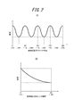
- FIG. 6 is a graph showing the circumferential profile of the film thickness of the epitaxial layer at the peripheral edge of the epitaxial wafer (position 1 mm inside from the outer peripheral edge of the epitaxial wafer) for Examples 2 and 8 and Comparative Example 8 in the same manner.
- FIG. 7 shows the relationship of the PV value to the chamfering width A1 on the front surface side of Examples 1 to 12 and Comparative Examples 1 to 12.
- FIG. 8C is a graph using the relative value when FIG. 8A is cycled 45 degrees and the film thickness at 0 degree is set to 1, and FIG. 8D is also similar to FIG. It is a graph in which B) is cycled 45 degrees and relative values are used.
- FIG. 9A and 9B show the measurement results of ESFQR in Examples 4 and 10 and Comparative Examples 4 and 10 at positions 1 mm and 1.5 mm inside from the outer peripheral edge of the epitaxial wafer, respectively.
- FIG. 9C is a graph in which FIG. 9A is cycled 45 degrees
- FIG. 9D is also a graph in which FIG. 9B is cycled 45 degrees.
- the variation in flatness becomes smaller as the length A1 of the chamfer width on the front surface side is shorter.
- FIG. 6 also shows that the shorter the A1 is, the more the growth rate orientation dependency can be suppressed, and the circumferential variation in the thickness of the epitaxial layer at the peripheral portion can be suppressed.
- the chamfering width of the end of the surface of the silicon wafer to be epitaxially grown is 200 ⁇ m or less and the epitaxial layer is formed after that, the growth rate orientation dependency can be suppressed, and the flatness at the peripheral portion can be reduced.
- a method for producing a high epitaxial silicon wafer and an epitaxial silicon wafer obtained thereby can be provided.
Landscapes
- Chemical & Material Sciences (AREA)
- Crystallography & Structural Chemistry (AREA)
- Engineering & Computer Science (AREA)
- Materials Engineering (AREA)
- Metallurgy (AREA)
- Organic Chemistry (AREA)
- Chemical Kinetics & Catalysis (AREA)
- General Chemical & Material Sciences (AREA)
- Chemical Vapour Deposition (AREA)
- Crystals, And After-Treatments Of Crystals (AREA)
Abstract
Description
すなわち、エピタキシャル成長させる面の結晶面が(100)面または(110)面である場合、既述の成長速度方位依存性が発現しうるが、成長させる面側の端部の面取り幅を、従来使用される範囲よりも狭い200μm以下にすることで成長速度方位依存性を抑制できることを見出した。このようなシリコンウェーハ上にエピタキシャル層を成長させれば、成長速度方位依存性を抑制して周縁部における平坦度の高いエピタキシャルシリコンウェーハを得られる。本発明者らはこのような知見に基づき、本発明を完成させるに至った。
本発明によるエピタキシャルシリコンウェーハの製造方法は、
片面の面方位が(100)面または(110)面であり、該片面側の端部の面取り幅が200μm以下であるシリコンウェーハの、前記片面上にエピタキシャル層を形成することを特徴とする。
記
PV値は、エッジ除外領域を1mmとしたESFQRの、結晶方位ごとの平均値のうち、最大値から最小値を差し引いた値(nm)を、前記シリコンウェーハの中心部における前記エピタキシャル層の膜厚(μm)で除した値とする。
片面の面方位が(100)面または(110)面であり、該片面側の端部の面取り幅が200μm以下であるシリコンウェーハと、
該シリコンウェーハの前記片面上に形成されたエピタキシャル層と、を有するエピタキシャルシリコンウェーハであって、
前記エピタキシャル層の表面において、下記に定義されるPV値が12.5以下であることを特徴とする。
記
PV値は、エッジ除外領域を1mmとしたESFQRの、結晶方位ごとの平均値のうち、最大値から最小値を差し引いた値(nm)を、前記シリコンウェーハの中心部における前記エピタキシャル層の膜厚(μm)で除した値とする。
これまで説明した製造方法により得られるエピタキシャルウェーハ1は、基板となるシリコンウェーハ2と、このシリコンウェーハ2の片面であるおもて面23上に形成されたエピタキシャル層3とを有する。ここで、シリコンウェーハ2のおもて面23の結晶面は(100)面または(100)面であり、おもて面23側の面取り幅長さA1は200μm以下である。このエピタキシャルシリコンウェーハ1の周縁部11の平坦度の指標である既述のPV値は12.5以下である。
直径300mm、厚さ775μmであり、おもて面側の端部の面取り幅A1が130μmに面取り加工したp型シリコンウェーハを作製した。シリコンウェーハのおもて面の結晶面は(100)面であり、裏面の面取り幅A2は350μmである。
おもて面側の端部の面取り幅A1および/またはエピタキシャル層の膜厚を表1に記載の値に変えたこと以外は、実施例1と同じ方法でエピタキシャルシリコンウェーハを作製した。

図4(B)は図4(A)を45度周期化したグラフである。
図5(B)は図5(A)を45度周期化したグラフである。
11 エピタキシャルシリコンウェーハの周縁部
2 シリコンウェーハ
21 エッジ領域
22 ベベル領域
23 おもて面
24 裏面
3 エピタキシャル層
4 シリコンソースガス
51 セクター
52 エッジ除外領域
Claims (8)
- 片面の面方位が(100)面または(110)面であり、該片面側の端部の面取り幅が200μm以下であるシリコンウェーハの、前記片面上にエピタキシャル層を形成することを特徴とするエピタキシャルシリコンウェーハの製造方法。
- 前記シリコンウェーハの中心部における前記エピタキシャル層の膜厚が2~10μmである請求項1に記載のエピタキシャルシリコンウェーハの製造方法。
- 前記シリコンウェーハの前記片面側の端部の面取り幅が100μm以上である請求項1または2に記載のエピタキシャルシリコンウェーハの製造方法。
- 前記シリコンウェーハの他面側の端部の面取り幅が300~400μmである請求項1~3のいずれか1項に記載のエピタキシャルシリコンウェーハの製造方法。
- 前記エピタキシャル層の形成では、前記エピタキシャル層の表面において、下記に定義されるPV値を12.5以下に制御することを特徴とする請求項1~4のいずれか1項に記載のエピタキシャルシリコンウェーハの製造方法。
記
PV値は、エッジ除外領域を1mmとしたESFQRの、結晶方位ごとの平均値のうち、最大値から最小値を差し引いた値(nm)を、前記シリコンウェーハの中心部における前記エピタキシャル層の膜厚(μm)で除した値とする。 - 片面の面方位が(100)面または(110)面であり、該片面側の端部の面取り幅が200μm以下であるシリコンウェーハと、
該シリコンウェーハの前記片面上に形成されたエピタキシャル層と、を有するエピタキシャルシリコンウェーハであって、
前記エピタキシャル層の表面において、下記に定義されるPV値が12.5以下であることを特徴とするエピタキシャルシリコンウェーハ。
記
PV値は、エッジ除外領域を1mmとしたESFQRの、結晶方位ごとの平均値のうち、最大値から最小値を差し引いた値(nm)を、前記シリコンウェーハの中心部における前記エピタキシャル層の膜厚(μm)で除した値とする。 - 前記シリコンウェーハの中心部における前記エピタキシャル層の膜厚が2~10μmである請求項6に記載のエピタキシャルシリコンウェーハ。
- 前記シリコンウェーハの他面側の端部の面取り幅が300~400μmである請求項6または7に記載のエピタキシャルシリコンウェーハ。
Priority Applications (3)
| Application Number | Priority Date | Filing Date | Title |
|---|---|---|---|
| US14/414,487 US9631297B2 (en) | 2012-08-09 | 2013-07-24 | Method of producing epitaxial silicon wafer and epitaxial silicon wafer |
| CN201380040947.9A CN104584191B (zh) | 2012-08-09 | 2013-07-24 | 外延硅晶片的制造方法和外延硅晶片 |
| KR1020157002970A KR101659380B1 (ko) | 2012-08-09 | 2013-07-24 | 에피택셜 실리콘 웨이퍼의 제조 방법 및 에피택셜 실리콘 웨이퍼 |
Applications Claiming Priority (2)
| Application Number | Priority Date | Filing Date | Title |
|---|---|---|---|
| JP2012177317A JP6035982B2 (ja) | 2012-08-09 | 2012-08-09 | エピタキシャルシリコンウェーハの製造方法およびエピタキシャルシリコンウェーハ |
| JP2012-177317 | 2012-08-09 |
Publications (1)
| Publication Number | Publication Date |
|---|---|
| WO2014024404A1 true WO2014024404A1 (ja) | 2014-02-13 |
Family
ID=50067666
Family Applications (1)
| Application Number | Title | Priority Date | Filing Date |
|---|---|---|---|
| PCT/JP2013/004506 Ceased WO2014024404A1 (ja) | 2012-08-09 | 2013-07-24 | エピタキシャルシリコンウェーハの製造方法およびエピタキシャルシリコンウェーハ |
Country Status (6)
| Country | Link |
|---|---|
| US (1) | US9631297B2 (ja) |
| JP (1) | JP6035982B2 (ja) |
| KR (1) | KR101659380B1 (ja) |
| CN (1) | CN104584191B (ja) |
| TW (1) | TWI531692B (ja) |
| WO (1) | WO2014024404A1 (ja) |
Cited By (1)
| Publication number | Priority date | Publication date | Assignee | Title |
|---|---|---|---|---|
| WO2016047046A1 (ja) * | 2014-09-26 | 2016-03-31 | 信越半導体株式会社 | 貼り合わせウェーハの製造方法 |
Families Citing this family (19)
| Publication number | Priority date | Publication date | Assignee | Title |
|---|---|---|---|---|
| JP6056749B2 (ja) * | 2013-12-25 | 2017-01-11 | 信越半導体株式会社 | エピタキシャル成長前後の半導体ウェーハのエッジ形状の評価方法 |
| KR20160112113A (ko) | 2015-03-18 | 2016-09-28 | 주식회사 엘지실트론 | 웨이퍼 제조 장치 |
| DE102015220924B4 (de) * | 2015-10-27 | 2018-09-27 | Siltronic Ag | Suszeptor zum Halten einer Halbleiterscheibe mit Orientierungskerbe, Verfahren zum Abscheiden einer Schicht auf einer Halbleiterscheibe und Halbleiterscheibe |
| DE102016210203B3 (de) * | 2016-06-09 | 2017-08-31 | Siltronic Ag | Suszeptor zum Halten einer Halbleiterscheibe, Verfahren zum Abscheiden einer epitaktischen Schicht auf einer Vorderseite einer Halbleiterscheibe und Halbleiterscheibe mit epitaktischer Schicht |
| JP6256576B1 (ja) * | 2016-11-17 | 2018-01-10 | 株式会社Sumco | エピタキシャルウェーハ及びその製造方法 |
| KR20180074273A (ko) * | 2016-12-23 | 2018-07-03 | 에스케이실트론 주식회사 | 에피텍셜 웨이퍼 제조 방법 및 장치 |
| DE102017210450A1 (de) * | 2017-06-21 | 2018-12-27 | Siltronic Ag | Verfahren, Steuerungssystem und Anlage zum Bearbeiten einer Halbleiterscheibe sowie Halbleiterscheibe |
| JP6717267B2 (ja) * | 2017-07-10 | 2020-07-01 | 株式会社Sumco | シリコンウェーハの製造方法 |
| JP6750592B2 (ja) * | 2017-08-15 | 2020-09-02 | 信越半導体株式会社 | シリコンウエーハのエッジ形状の評価方法および評価装置、シリコンウエーハ、ならびにその選別方法および製造方法 |
| CN109545653A (zh) * | 2017-09-22 | 2019-03-29 | 上海新昇半导体科技有限公司 | 改善外延硅片边缘平坦度的方法 |
| DE102017222279A1 (de) | 2017-12-08 | 2019-06-13 | Siltronic Ag | Verfahren zum Abscheiden einer epitaktischen Schicht auf einer Vorderseite einer Halbleiterscheibe und Vorrichtung zur Durchführung des Verfahrens |
| JP6881283B2 (ja) * | 2017-12-27 | 2021-06-02 | 株式会社Sumco | エピタキシャルシリコンウェーハの製造方法およびエピタキシャルシリコンウェーハ |
| DE102018200415A1 (de) | 2018-01-11 | 2019-07-11 | Siltronic Ag | Halbleiterscheibe mit epitaktischer Schicht |
| CN108950680A (zh) * | 2018-08-09 | 2018-12-07 | 上海新昇半导体科技有限公司 | 外延基座及外延设备 |
| DE102019207772A1 (de) | 2019-05-28 | 2020-12-03 | Siltronic Ag | Verfahren zum Abscheiden einer epitaktischen Schicht auf einer Vorderseite einer Halbleiterscheibe und Vorrichtung zur Durchführung des Verfahrens |
| CN110592665A (zh) * | 2019-08-09 | 2019-12-20 | 上海新昇半导体科技有限公司 | 一种半导体薄膜平坦度改善的方法 |
| KR102413432B1 (ko) * | 2020-08-28 | 2022-06-27 | 에스케이실트론 주식회사 | 웨이퍼 및 그 형상 분석 방법 |
| EP4170700A4 (en) * | 2021-09-07 | 2024-01-03 | JX Nippon Mining & Metals Corporation | INDIUM PHOSPHIDE SUBSTRATE |
| WO2025098595A1 (en) * | 2023-11-07 | 2025-05-15 | Ams-Osram International Gmbh | Growth substrate and method for processing an optoelectronic device |
Citations (3)
| Publication number | Priority date | Publication date | Assignee | Title |
|---|---|---|---|---|
| WO2010035510A1 (ja) * | 2008-09-29 | 2010-04-01 | 株式会社Sumco | シリコンウェーハおよびその製造方法 |
| JP2011249675A (ja) * | 2010-05-28 | 2011-12-08 | Showa Denko Kk | 半導体発光素子の製造方法 |
| JP2012142485A (ja) * | 2011-01-05 | 2012-07-26 | Sumco Corp | エピタキシャルウェーハの製造方法、エピタキシャルウェーハ |
Family Cites Families (12)
| Publication number | Priority date | Publication date | Assignee | Title |
|---|---|---|---|---|
| JPH04122023A (ja) | 1990-09-13 | 1992-04-22 | Hitachi Ltd | 半導体ウエハの製造方法および半導体集積回路装置の製造方法 |
| JP2827885B2 (ja) * | 1994-02-12 | 1998-11-25 | 信越半導体株式会社 | 半導体単結晶基板およびその製造方法 |
| JP2000269147A (ja) | 1999-03-18 | 2000-09-29 | Shin Etsu Handotai Co Ltd | 気相成長装置、気相成長方法及びシリコンエピタキシャルウェーハ |
| JP4959878B2 (ja) * | 2001-05-10 | 2012-06-27 | オンセミコンダクター・トレーディング・リミテッド | ウエファの製造方法 |
| JP2003124219A (ja) * | 2001-10-10 | 2003-04-25 | Sumitomo Mitsubishi Silicon Corp | シリコンウエーハおよびエピタキシャルシリコンウエーハ |
| JP4815801B2 (ja) * | 2004-12-28 | 2011-11-16 | 信越半導体株式会社 | シリコンウエーハの研磨方法および製造方法および円板状ワークの研磨装置ならびにシリコンウエーハ |
| JP4868522B2 (ja) * | 2006-03-30 | 2012-02-01 | Sumco Techxiv株式会社 | エピタキシャルウェーハの製造方法及び製造装置 |
| WO2009060914A1 (ja) * | 2007-11-08 | 2009-05-14 | Sumco Corporation | エピタキシャルウェーハ |
| US7998867B2 (en) * | 2007-11-08 | 2011-08-16 | Sumco Corporation | Method for manufacturing epitaxial wafer |
| JP2009283650A (ja) | 2008-05-22 | 2009-12-03 | Sumco Corp | 半導体ウェーハの再生方法 |
| IT1402357B1 (it) * | 2010-09-17 | 2013-08-30 | Marana Forni Di Marana Ferdinando | Forno ad elevato rendimento per la cottura di cibi |
| JP5644401B2 (ja) | 2010-11-15 | 2014-12-24 | 株式会社Sumco | エピタキシャルウェーハの製造方法およびエピタキシャルウェーハ |
-
2012
- 2012-08-09 JP JP2012177317A patent/JP6035982B2/ja active Active
-
2013
- 2013-07-24 WO PCT/JP2013/004506 patent/WO2014024404A1/ja not_active Ceased
- 2013-07-24 US US14/414,487 patent/US9631297B2/en active Active
- 2013-07-24 CN CN201380040947.9A patent/CN104584191B/zh active Active
- 2013-07-24 KR KR1020157002970A patent/KR101659380B1/ko active Active
- 2013-07-31 TW TW102127355A patent/TWI531692B/zh active
Patent Citations (3)
| Publication number | Priority date | Publication date | Assignee | Title |
|---|---|---|---|---|
| WO2010035510A1 (ja) * | 2008-09-29 | 2010-04-01 | 株式会社Sumco | シリコンウェーハおよびその製造方法 |
| JP2011249675A (ja) * | 2010-05-28 | 2011-12-08 | Showa Denko Kk | 半導体発光素子の製造方法 |
| JP2012142485A (ja) * | 2011-01-05 | 2012-07-26 | Sumco Corp | エピタキシャルウェーハの製造方法、エピタキシャルウェーハ |
Cited By (3)
| Publication number | Priority date | Publication date | Assignee | Title |
|---|---|---|---|---|
| WO2016047046A1 (ja) * | 2014-09-26 | 2016-03-31 | 信越半導体株式会社 | 貼り合わせウェーハの製造方法 |
| JP2016072267A (ja) * | 2014-09-26 | 2016-05-09 | 信越半導体株式会社 | 貼り合わせウェーハの製造方法 |
| US9842763B2 (en) | 2014-09-26 | 2017-12-12 | Shin-Etsu Handotai Co., Ltd. | Method for manufacturing bonded wafer |
Also Published As
| Publication number | Publication date |
|---|---|
| TW201413074A (zh) | 2014-04-01 |
| KR20150023940A (ko) | 2015-03-05 |
| CN104584191B (zh) | 2017-03-29 |
| JP6035982B2 (ja) | 2016-11-30 |
| JP2014036153A (ja) | 2014-02-24 |
| US9631297B2 (en) | 2017-04-25 |
| TWI531692B (zh) | 2016-05-01 |
| US20150184314A1 (en) | 2015-07-02 |
| CN104584191A (zh) | 2015-04-29 |
| KR101659380B1 (ko) | 2016-09-23 |
Similar Documents
| Publication | Publication Date | Title |
|---|---|---|
| JP6035982B2 (ja) | エピタキシャルシリコンウェーハの製造方法およびエピタキシャルシリコンウェーハ | |
| CN105378894B (zh) | 外延晶片的制造方法 | |
| JP5834632B2 (ja) | サセプタ、該サセプタを用いた気相成長装置およびエピタキシャルウェーハの製造方法 | |
| KR20090055567A (ko) | 탄화규소 기판의 제조 방법 및 탄화규소 기판 | |
| WO2015114974A1 (ja) | シリコンウェーハ | |
| JP6150075B2 (ja) | エピタキシャルウェーハの製造方法 | |
| US11990336B2 (en) | Silicon epitaxial wafer production method and silicon epitaxial wafer | |
| JP6881283B2 (ja) | エピタキシャルシリコンウェーハの製造方法およびエピタキシャルシリコンウェーハ | |
| JP7596707B2 (ja) | 炭化珪素多結晶膜の成膜方法および炭化珪素多結晶基板の製造方法 | |
| CN113302718B (zh) | 硅外延晶片的制造方法和硅外延晶片 | |
| WO2011145279A1 (ja) | シリコンエピタキシャルウェーハ及びその製造方法 | |
| JP2004099415A (ja) | 単結晶、単結晶ウエーハ及びエピタキシャルウエーハ、並びに単結晶育成方法 | |
| JP7151664B2 (ja) | エピタキシャルウェーハの製造方法 | |
| US9633843B2 (en) | Silicon substrates with compressive stress and methods for production of the same | |
| JP6924593B2 (ja) | エピタキシャルウェーハの製造方法 | |
| JP2021082641A (ja) | エピタキシャルウェーハの製造方法及びエピタキシャルウェーハ | |
| JP4911042B2 (ja) | 単結晶ウエーハ及びエピタキシャルウエーハ | |
| KR20210014340A (ko) | 웨이퍼의 에피택셜층의 성장 온도 설정 방법 및 에피택셜층의 성장 방법 | |
| JP5453967B2 (ja) | エピタキシャルウェーハおよびその製造方法 | |
| JP7600612B2 (ja) | 炭化珪素多結晶膜の成膜方法および炭化珪素多結晶基板の製造方法 | |
| JP2023113512A (ja) | エピタキシャルウェーハの製造方法 | |
| WO2025094485A1 (ja) | エピタキシャルシリコンウェーハ及びその製造方法 |
Legal Events
| Date | Code | Title | Description |
|---|---|---|---|
| 121 | Ep: the epo has been informed by wipo that ep was designated in this application |
Ref document number: 13828170 Country of ref document: EP Kind code of ref document: A1 |
|
| WWE | Wipo information: entry into national phase |
Ref document number: 14414487 Country of ref document: US |
|
| ENP | Entry into the national phase |
Ref document number: 20157002970 Country of ref document: KR Kind code of ref document: A |
|
| NENP | Non-entry into the national phase |
Ref country code: DE |
|
| 122 | Ep: pct application non-entry in european phase |
Ref document number: 13828170 Country of ref document: EP Kind code of ref document: A1 |