WO2014017334A1 - 蛍光体シート - Google Patents
蛍光体シート Download PDFInfo
- Publication number
- WO2014017334A1 WO2014017334A1 PCT/JP2013/069289 JP2013069289W WO2014017334A1 WO 2014017334 A1 WO2014017334 A1 WO 2014017334A1 JP 2013069289 W JP2013069289 W JP 2013069289W WO 2014017334 A1 WO2014017334 A1 WO 2014017334A1
- Authority
- WO
- WIPO (PCT)
- Prior art keywords
- phosphor
- silicon dioxide
- coated
- sulfide
- dioxide film
- Prior art date
Links
- OAICVXFJPJFONN-UHFFFAOYSA-N Phosphorus Chemical compound [P] OAICVXFJPJFONN-UHFFFAOYSA-N 0.000 title claims abstract description 324
- VYPSYNLAJGMNEJ-UHFFFAOYSA-N Silicium dioxide Chemical compound O=[Si]=O VYPSYNLAJGMNEJ-UHFFFAOYSA-N 0.000 claims abstract description 139
- UCKMPCXJQFINFW-UHFFFAOYSA-N Sulphide Chemical compound [S-2] UCKMPCXJQFINFW-UHFFFAOYSA-N 0.000 claims abstract description 80
- 239000000377 silicon dioxide Substances 0.000 claims abstract description 68
- 235000012239 silicon dioxide Nutrition 0.000 claims abstract description 67
- 239000000843 powder Substances 0.000 claims abstract description 54
- 229910044991 metal oxide Inorganic materials 0.000 claims abstract description 50
- 150000004706 metal oxides Chemical class 0.000 claims abstract description 50
- 239000011342 resin composition Substances 0.000 claims abstract description 34
- 239000003505 polymerization initiator Substances 0.000 claims abstract description 21
- 150000001875 compounds Chemical class 0.000 claims abstract description 19
- 239000000758 substrate Substances 0.000 claims description 34
- 229920005989 resin Polymers 0.000 claims description 17
- 239000011347 resin Substances 0.000 claims description 17
- NIXOWILDQLNWCW-UHFFFAOYSA-M Acrylate Chemical compound [O-]C(=O)C=C NIXOWILDQLNWCW-UHFFFAOYSA-M 0.000 claims description 11
- XLOMVQKBTHCTTD-UHFFFAOYSA-N Zinc monoxide Chemical group [Zn]=O XLOMVQKBTHCTTD-UHFFFAOYSA-N 0.000 claims description 8
- 239000011248 coating agent Substances 0.000 claims description 8
- 238000000576 coating method Methods 0.000 claims description 8
- 239000003999 initiator Substances 0.000 claims description 7
- 229910052791 calcium Inorganic materials 0.000 claims description 2
- 229910052749 magnesium Inorganic materials 0.000 claims description 2
- NINIDFKCEFEMDL-UHFFFAOYSA-N Sulfur Chemical compound [S] NINIDFKCEFEMDL-UHFFFAOYSA-N 0.000 abstract description 33
- 229910052717 sulfur Inorganic materials 0.000 abstract description 33
- 239000011593 sulfur Substances 0.000 abstract description 33
- 230000006866 deterioration Effects 0.000 abstract description 14
- 239000002245 particle Substances 0.000 abstract description 9
- 230000007797 corrosion Effects 0.000 abstract description 7
- 238000005260 corrosion Methods 0.000 abstract description 7
- 239000010408 film Substances 0.000 description 106
- 239000010410 layer Substances 0.000 description 49
- 239000007789 gas Substances 0.000 description 31
- 238000007789 sealing Methods 0.000 description 22
- 238000000034 method Methods 0.000 description 18
- LFQSCWFLJHTTHZ-UHFFFAOYSA-N Ethanol Chemical compound CCO LFQSCWFLJHTTHZ-UHFFFAOYSA-N 0.000 description 16
- XLYOFNOQVPJJNP-UHFFFAOYSA-N water Chemical compound O XLYOFNOQVPJJNP-UHFFFAOYSA-N 0.000 description 15
- 239000003054 catalyst Substances 0.000 description 12
- 239000000126 substance Substances 0.000 description 12
- 239000002585 base Substances 0.000 description 10
- 239000000463 material Substances 0.000 description 10
- BQCADISMDOOEFD-UHFFFAOYSA-N Silver Chemical compound [Ag] BQCADISMDOOEFD-UHFFFAOYSA-N 0.000 description 9
- 230000000052 comparative effect Effects 0.000 description 9
- 230000007062 hydrolysis Effects 0.000 description 9
- 238000006460 hydrolysis reaction Methods 0.000 description 9
- 229910052709 silver Inorganic materials 0.000 description 9
- 239000004332 silver Substances 0.000 description 9
- 239000012790 adhesive layer Substances 0.000 description 8
- 230000005284 excitation Effects 0.000 description 8
- 238000004519 manufacturing process Methods 0.000 description 8
- 238000011156 evaluation Methods 0.000 description 7
- 238000002156 mixing Methods 0.000 description 7
- 239000002904 solvent Substances 0.000 description 7
- 239000004973 liquid crystal related substance Substances 0.000 description 6
- 239000002356 single layer Substances 0.000 description 6
- 239000007790 solid phase Substances 0.000 description 6
- JOYRKODLDBILNP-UHFFFAOYSA-N Ethyl urethane Chemical compound CCOC(N)=O JOYRKODLDBILNP-UHFFFAOYSA-N 0.000 description 5
- -1 hexafluoroarsenic acid Chemical compound 0.000 description 5
- 238000005286 illumination Methods 0.000 description 5
- 230000008569 process Effects 0.000 description 5
- 238000003756 stirring Methods 0.000 description 5
- QVGXLLKOCUKJST-UHFFFAOYSA-N atomic oxygen Chemical compound [O] QVGXLLKOCUKJST-UHFFFAOYSA-N 0.000 description 4
- IJKVHSBPTUYDLN-UHFFFAOYSA-N dihydroxy(oxo)silane Chemical compound O[Si](O)=O IJKVHSBPTUYDLN-UHFFFAOYSA-N 0.000 description 4
- 239000012788 optical film Substances 0.000 description 4
- 229910052760 oxygen Inorganic materials 0.000 description 4
- 239000001301 oxygen Substances 0.000 description 4
- 229920005862 polyol Polymers 0.000 description 4
- 150000003077 polyols Chemical class 0.000 description 4
- 230000001681 protective effect Effects 0.000 description 4
- LIVNPJMFVYWSIS-UHFFFAOYSA-N silicon monoxide Chemical compound [Si-]#[O+] LIVNPJMFVYWSIS-UHFFFAOYSA-N 0.000 description 4
- QTBSBXVTEAMEQO-UHFFFAOYSA-N Acetic acid Chemical compound CC(O)=O QTBSBXVTEAMEQO-UHFFFAOYSA-N 0.000 description 3
- 229910015802 BaSr Inorganic materials 0.000 description 3
- LYCAIKOWRPUZTN-UHFFFAOYSA-N Ethylene glycol Chemical compound OCCO LYCAIKOWRPUZTN-UHFFFAOYSA-N 0.000 description 3
- OKKJLVBELUTLKV-UHFFFAOYSA-N Methanol Chemical compound OC OKKJLVBELUTLKV-UHFFFAOYSA-N 0.000 description 3
- MUBZPKHOEPUJKR-UHFFFAOYSA-N Oxalic acid Chemical compound OC(=O)C(O)=O MUBZPKHOEPUJKR-UHFFFAOYSA-N 0.000 description 3
- DNIAPMSPPWPWGF-UHFFFAOYSA-N Propylene glycol Chemical compound CC(O)CO DNIAPMSPPWPWGF-UHFFFAOYSA-N 0.000 description 3
- HEMHJVSKTPXQMS-UHFFFAOYSA-M Sodium hydroxide Chemical compound [OH-].[Na+] HEMHJVSKTPXQMS-UHFFFAOYSA-M 0.000 description 3
- BOTDANWDWHJENH-UHFFFAOYSA-N Tetraethyl orthosilicate Chemical compound CCO[Si](OCC)(OCC)OCC BOTDANWDWHJENH-UHFFFAOYSA-N 0.000 description 3
- HCHKCACWOHOZIP-UHFFFAOYSA-N Zinc Chemical compound [Zn] HCHKCACWOHOZIP-UHFFFAOYSA-N 0.000 description 3
- 230000002378 acidificating effect Effects 0.000 description 3
- 239000000853 adhesive Substances 0.000 description 3
- 230000001070 adhesive effect Effects 0.000 description 3
- 230000004888 barrier function Effects 0.000 description 3
- 230000015572 biosynthetic process Effects 0.000 description 3
- 238000007796 conventional method Methods 0.000 description 3
- MTHSVFCYNBDYFN-UHFFFAOYSA-N diethylene glycol Chemical compound OCCOCCO MTHSVFCYNBDYFN-UHFFFAOYSA-N 0.000 description 3
- 238000009792 diffusion process Methods 0.000 description 3
- 238000010304 firing Methods 0.000 description 3
- 239000011521 glass Substances 0.000 description 3
- 239000007791 liquid phase Substances 0.000 description 3
- 238000005259 measurement Methods 0.000 description 3
- 239000011259 mixed solution Substances 0.000 description 3
- 239000000203 mixture Substances 0.000 description 3
- 229920001721 polyimide Polymers 0.000 description 3
- 238000000926 separation method Methods 0.000 description 3
- 229910052814 silicon oxide Inorganic materials 0.000 description 3
- 229910052725 zinc Inorganic materials 0.000 description 3
- 239000011701 zinc Substances 0.000 description 3
- CSCPPACGZOOCGX-UHFFFAOYSA-N Acetone Chemical compound CC(C)=O CSCPPACGZOOCGX-UHFFFAOYSA-N 0.000 description 2
- QGZKDVFQNNGYKY-UHFFFAOYSA-N Ammonia Chemical compound N QGZKDVFQNNGYKY-UHFFFAOYSA-N 0.000 description 2
- VHUUQVKOLVNVRT-UHFFFAOYSA-N Ammonium hydroxide Chemical compound [NH4+].[OH-] VHUUQVKOLVNVRT-UHFFFAOYSA-N 0.000 description 2
- RTZKZFJDLAIYFH-UHFFFAOYSA-N Diethyl ether Chemical compound CCOCC RTZKZFJDLAIYFH-UHFFFAOYSA-N 0.000 description 2
- RWSOTUBLDIXVET-UHFFFAOYSA-N Dihydrogen sulfide Chemical compound S RWSOTUBLDIXVET-UHFFFAOYSA-N 0.000 description 2
- VEXZGXHMUGYJMC-UHFFFAOYSA-N Hydrochloric acid Chemical compound Cl VEXZGXHMUGYJMC-UHFFFAOYSA-N 0.000 description 2
- AFVFQIVMOAPDHO-UHFFFAOYSA-N Methanesulfonic acid Chemical compound CS(O)(=O)=O AFVFQIVMOAPDHO-UHFFFAOYSA-N 0.000 description 2
- AMQJEAYHLZJPGS-UHFFFAOYSA-N N-Pentanol Chemical compound CCCCCO AMQJEAYHLZJPGS-UHFFFAOYSA-N 0.000 description 2
- 239000004642 Polyimide Substances 0.000 description 2
- 239000004721 Polyphenylene oxide Substances 0.000 description 2
- 239000006087 Silane Coupling Agent Substances 0.000 description 2
- QAOWNCQODCNURD-UHFFFAOYSA-N Sulfuric acid Chemical compound OS(O)(=O)=O QAOWNCQODCNURD-UHFFFAOYSA-N 0.000 description 2
- RAHZWNYVWXNFOC-UHFFFAOYSA-N Sulphur dioxide Chemical compound O=S=O RAHZWNYVWXNFOC-UHFFFAOYSA-N 0.000 description 2
- NIXOWILDQLNWCW-UHFFFAOYSA-N acrylic acid group Chemical group C(C=C)(=O)O NIXOWILDQLNWCW-UHFFFAOYSA-N 0.000 description 2
- 230000009471 action Effects 0.000 description 2
- 239000003463 adsorbent Substances 0.000 description 2
- 235000011114 ammonium hydroxide Nutrition 0.000 description 2
- 229910052788 barium Inorganic materials 0.000 description 2
- 230000015556 catabolic process Effects 0.000 description 2
- 238000006243 chemical reaction Methods 0.000 description 2
- 239000003086 colorant Substances 0.000 description 2
- 238000006731 degradation reaction Methods 0.000 description 2
- 238000001035 drying Methods 0.000 description 2
- 230000000694 effects Effects 0.000 description 2
- 230000001747 exhibiting effect Effects 0.000 description 2
- 229910000037 hydrogen sulfide Inorganic materials 0.000 description 2
- 230000001678 irradiating effect Effects 0.000 description 2
- 238000010030 laminating Methods 0.000 description 2
- WABPQHHGFIMREM-UHFFFAOYSA-N lead(0) Chemical compound [Pb] WABPQHHGFIMREM-UHFFFAOYSA-N 0.000 description 2
- 229910052751 metal Inorganic materials 0.000 description 2
- 239000002184 metal Substances 0.000 description 2
- 239000003960 organic solvent Substances 0.000 description 2
- VLTRZXGMWDSKGL-UHFFFAOYSA-N perchloric acid Chemical compound OCl(=O)(=O)=O VLTRZXGMWDSKGL-UHFFFAOYSA-N 0.000 description 2
- 229920000728 polyester Polymers 0.000 description 2
- 229920000139 polyethylene terephthalate Polymers 0.000 description 2
- 239000005020 polyethylene terephthalate Substances 0.000 description 2
- 229920000098 polyolefin Polymers 0.000 description 2
- 239000000047 product Substances 0.000 description 2
- 238000001179 sorption measurement Methods 0.000 description 2
- 238000000967 suction filtration Methods 0.000 description 2
- 150000005846 sugar alcohols Polymers 0.000 description 2
- RBORURQQJIQWBS-QVRNUERCSA-N (4ar,6r,7r,7as)-6-(6-amino-8-bromopurin-9-yl)-2-hydroxy-2-sulfanylidene-4a,6,7,7a-tetrahydro-4h-furo[3,2-d][1,3,2]dioxaphosphinin-7-ol Chemical compound C([C@H]1O2)OP(O)(=S)O[C@H]1[C@@H](O)[C@@H]2N1C(N=CN=C2N)=C2N=C1Br RBORURQQJIQWBS-QVRNUERCSA-N 0.000 description 1
- JYEUMXHLPRZUAT-UHFFFAOYSA-N 1,2,3-triazine Chemical compound C1=CN=NN=C1 JYEUMXHLPRZUAT-UHFFFAOYSA-N 0.000 description 1
- XQUPVDVFXZDTLT-UHFFFAOYSA-N 1-[4-[[4-(2,5-dioxopyrrol-1-yl)phenyl]methyl]phenyl]pyrrole-2,5-dione Chemical compound O=C1C=CC(=O)N1C(C=C1)=CC=C1CC1=CC=C(N2C(C=CC2=O)=O)C=C1 XQUPVDVFXZDTLT-UHFFFAOYSA-N 0.000 description 1
- RIWRBSMFKVOJMN-UHFFFAOYSA-N 2-methyl-1-phenylpropan-2-ol Chemical compound CC(C)(O)CC1=CC=CC=C1 RIWRBSMFKVOJMN-UHFFFAOYSA-N 0.000 description 1
- BMYNFMYTOJXKLE-UHFFFAOYSA-N 3-azaniumyl-2-hydroxypropanoate Chemical compound NCC(O)C(O)=O BMYNFMYTOJXKLE-UHFFFAOYSA-N 0.000 description 1
- 239000004925 Acrylic resin Substances 0.000 description 1
- 229920000178 Acrylic resin Polymers 0.000 description 1
- 229910018072 Al 2 O 3 Inorganic materials 0.000 description 1
- 229920002284 Cellulose triacetate Polymers 0.000 description 1
- 239000004593 Epoxy Substances 0.000 description 1
- 108010043121 Green Fluorescent Proteins Proteins 0.000 description 1
- 239000005058 Isophorone diisocyanate Substances 0.000 description 1
- GRYLNZFGIOXLOG-UHFFFAOYSA-N Nitric acid Chemical compound O[N+]([O-])=O GRYLNZFGIOXLOG-UHFFFAOYSA-N 0.000 description 1
- ISWSIDIOOBJBQZ-UHFFFAOYSA-N Phenol Chemical compound OC1=CC=CC=C1 ISWSIDIOOBJBQZ-UHFFFAOYSA-N 0.000 description 1
- 239000004952 Polyamide Substances 0.000 description 1
- 241001085205 Prenanthella exigua Species 0.000 description 1
- NNLVGZFZQQXQNW-ADJNRHBOSA-N [(2r,3r,4s,5r,6s)-4,5-diacetyloxy-3-[(2s,3r,4s,5r,6r)-3,4,5-triacetyloxy-6-(acetyloxymethyl)oxan-2-yl]oxy-6-[(2r,3r,4s,5r,6s)-4,5,6-triacetyloxy-2-(acetyloxymethyl)oxan-3-yl]oxyoxan-2-yl]methyl acetate Chemical compound O([C@@H]1O[C@@H]([C@H]([C@H](OC(C)=O)[C@H]1OC(C)=O)O[C@H]1[C@@H]([C@@H](OC(C)=O)[C@H](OC(C)=O)[C@@H](COC(C)=O)O1)OC(C)=O)COC(=O)C)[C@@H]1[C@@H](COC(C)=O)O[C@@H](OC(C)=O)[C@H](OC(C)=O)[C@H]1OC(C)=O NNLVGZFZQQXQNW-ADJNRHBOSA-N 0.000 description 1
- 150000001242 acetic acid derivatives Chemical class 0.000 description 1
- 239000002253 acid Substances 0.000 description 1
- 150000001252 acrylic acid derivatives Chemical class 0.000 description 1
- 150000008044 alkali metal hydroxides Chemical class 0.000 description 1
- 125000000217 alkyl group Chemical group 0.000 description 1
- 125000003277 amino group Chemical group 0.000 description 1
- 229910021529 ammonia Inorganic materials 0.000 description 1
- 230000005540 biological transmission Effects 0.000 description 1
- 230000004397 blinking Effects 0.000 description 1
- KGBXLFKZBHKPEV-UHFFFAOYSA-N boric acid Chemical compound OB(O)O KGBXLFKZBHKPEV-UHFFFAOYSA-N 0.000 description 1
- 239000004327 boric acid Substances 0.000 description 1
- 238000010538 cationic polymerization reaction Methods 0.000 description 1
- 230000008859 change Effects 0.000 description 1
- 239000007795 chemical reaction product Substances 0.000 description 1
- 238000004040 coloring Methods 0.000 description 1
- 238000010276 construction Methods 0.000 description 1
- 238000003851 corona treatment Methods 0.000 description 1
- KOMDZQSPRDYARS-UHFFFAOYSA-N cyclopenta-1,3-diene titanium Chemical compound [Ti].C1C=CC=C1.C1C=CC=C1 KOMDZQSPRDYARS-UHFFFAOYSA-N 0.000 description 1
- 230000002542 deteriorative effect Effects 0.000 description 1
- 239000012954 diazonium Substances 0.000 description 1
- IJGRMHOSHXDMSA-UHFFFAOYSA-O diazynium Chemical compound [NH+]#N IJGRMHOSHXDMSA-UHFFFAOYSA-O 0.000 description 1
- 208000028659 discharge Diseases 0.000 description 1
- 238000002845 discoloration Methods 0.000 description 1
- 239000012776 electronic material Substances 0.000 description 1
- 230000007613 environmental effect Effects 0.000 description 1
- 125000004185 ester group Chemical group 0.000 description 1
- HHFAWKCIHAUFRX-UHFFFAOYSA-N ethoxide Chemical compound CC[O-] HHFAWKCIHAUFRX-UHFFFAOYSA-N 0.000 description 1
- MHCLJIVVJQQNKQ-UHFFFAOYSA-N ethyl carbamate;2-methylprop-2-enoic acid Chemical compound CCOC(N)=O.CC(=C)C(O)=O MHCLJIVVJQQNKQ-UHFFFAOYSA-N 0.000 description 1
- UHESRSKEBRADOO-UHFFFAOYSA-N ethyl carbamate;prop-2-enoic acid Chemical compound OC(=O)C=C.CCOC(N)=O UHESRSKEBRADOO-UHFFFAOYSA-N 0.000 description 1
- 238000000605 extraction Methods 0.000 description 1
- 239000004744 fabric Substances 0.000 description 1
- 125000002768 hydroxyalkyl group Chemical group 0.000 description 1
- 230000001771 impaired effect Effects 0.000 description 1
- 230000000977 initiatory effect Effects 0.000 description 1
- 238000009413 insulation Methods 0.000 description 1
- 230000009545 invasion Effects 0.000 description 1
- MGFYSGNNHQQTJW-UHFFFAOYSA-N iodonium Chemical compound [IH2+] MGFYSGNNHQQTJW-UHFFFAOYSA-N 0.000 description 1
- NIMLQBUJDJZYEJ-UHFFFAOYSA-N isophorone diisocyanate Chemical compound CC1(C)CC(N=C=O)CC(C)(CN=C=O)C1 NIMLQBUJDJZYEJ-UHFFFAOYSA-N 0.000 description 1
- 150000002576 ketones Chemical class 0.000 description 1
- 238000004898 kneading Methods 0.000 description 1
- 230000007774 longterm Effects 0.000 description 1
- 229940098779 methanesulfonic acid Drugs 0.000 description 1
- NBTOZLQBSIZIKS-UHFFFAOYSA-N methoxide Chemical compound [O-]C NBTOZLQBSIZIKS-UHFFFAOYSA-N 0.000 description 1
- 239000000178 monomer Substances 0.000 description 1
- 229910017604 nitric acid Inorganic materials 0.000 description 1
- 235000006408 oxalic acid Nutrition 0.000 description 1
- TWNQGVIAIRXVLR-UHFFFAOYSA-N oxo(oxoalumanyloxy)alumane Chemical compound O=[Al]O[Al]=O TWNQGVIAIRXVLR-UHFFFAOYSA-N 0.000 description 1
- 230000035515 penetration Effects 0.000 description 1
- 230000035699 permeability Effects 0.000 description 1
- 239000000049 pigment Substances 0.000 description 1
- 238000005498 polishing Methods 0.000 description 1
- 229920003192 poly(bis maleimide) Polymers 0.000 description 1
- 229920002492 poly(sulfone) Polymers 0.000 description 1
- 229920002647 polyamide Polymers 0.000 description 1
- 229920000515 polycarbonate Polymers 0.000 description 1
- 239000004417 polycarbonate Substances 0.000 description 1
- 238000006068 polycondensation reaction Methods 0.000 description 1
- 229920006267 polyester film Polymers 0.000 description 1
- 229920005906 polyester polyol Polymers 0.000 description 1
- 229920000570 polyether Polymers 0.000 description 1
- 229920006380 polyphenylene oxide Polymers 0.000 description 1
- 239000011164 primary particle Substances 0.000 description 1
- KCTAWXVAICEBSD-UHFFFAOYSA-N prop-2-enoyloxy prop-2-eneperoxoate Chemical compound C=CC(=O)OOOC(=O)C=C KCTAWXVAICEBSD-UHFFFAOYSA-N 0.000 description 1
- 230000000644 propagated effect Effects 0.000 description 1
- BDERNNFJNOPAEC-UHFFFAOYSA-N propan-1-ol Chemical compound CCCO BDERNNFJNOPAEC-UHFFFAOYSA-N 0.000 description 1
- OGHBATFHNDZKSO-UHFFFAOYSA-N propan-2-olate Chemical compound CC(C)[O-] OGHBATFHNDZKSO-UHFFFAOYSA-N 0.000 description 1
- 239000011241 protective layer Substances 0.000 description 1
- 239000007870 radical polymerization initiator Substances 0.000 description 1
- 239000011163 secondary particle Substances 0.000 description 1
- 150000003377 silicon compounds Chemical class 0.000 description 1
- 238000003980 solgel method Methods 0.000 description 1
- 229910052712 strontium Inorganic materials 0.000 description 1
- RWSOTUBLDIXVET-UHFFFAOYSA-O sulfonium Chemical compound [SH3+] RWSOTUBLDIXVET-UHFFFAOYSA-O 0.000 description 1
- 230000001629 suppression Effects 0.000 description 1
- 238000012360 testing method Methods 0.000 description 1
- LFQCEHFDDXELDD-UHFFFAOYSA-N tetramethyl orthosilicate Chemical compound CO[Si](OC)(OC)OC LFQCEHFDDXELDD-UHFFFAOYSA-N 0.000 description 1
- 229920005992 thermoplastic resin Polymers 0.000 description 1
- 125000003396 thiol group Chemical group [H]S* 0.000 description 1
- 238000002834 transmittance Methods 0.000 description 1
- 238000004506 ultrasonic cleaning Methods 0.000 description 1
- 238000007740 vapor deposition Methods 0.000 description 1
- 238000005303 weighing Methods 0.000 description 1
- 239000011787 zinc oxide Substances 0.000 description 1
Images


Classifications
-
- C—CHEMISTRY; METALLURGY
- C08—ORGANIC MACROMOLECULAR COMPOUNDS; THEIR PREPARATION OR CHEMICAL WORKING-UP; COMPOSITIONS BASED THEREON
- C08F—MACROMOLECULAR COMPOUNDS OBTAINED BY REACTIONS ONLY INVOLVING CARBON-TO-CARBON UNSATURATED BONDS
- C08F2/00—Processes of polymerisation
- C08F2/46—Polymerisation initiated by wave energy or particle radiation
- C08F2/48—Polymerisation initiated by wave energy or particle radiation by ultraviolet or visible light
-
- C—CHEMISTRY; METALLURGY
- C09—DYES; PAINTS; POLISHES; NATURAL RESINS; ADHESIVES; COMPOSITIONS NOT OTHERWISE PROVIDED FOR; APPLICATIONS OF MATERIALS NOT OTHERWISE PROVIDED FOR
- C09K—MATERIALS FOR MISCELLANEOUS APPLICATIONS, NOT PROVIDED FOR ELSEWHERE
- C09K11/00—Luminescent, e.g. electroluminescent, chemiluminescent materials
- C09K11/02—Use of particular materials as binders, particle coatings or suspension media therefor
- C09K11/025—Use of particular materials as binders, particle coatings or suspension media therefor non-luminescent particle coatings or suspension media
-
- C—CHEMISTRY; METALLURGY
- C09—DYES; PAINTS; POLISHES; NATURAL RESINS; ADHESIVES; COMPOSITIONS NOT OTHERWISE PROVIDED FOR; APPLICATIONS OF MATERIALS NOT OTHERWISE PROVIDED FOR
- C09K—MATERIALS FOR MISCELLANEOUS APPLICATIONS, NOT PROVIDED FOR ELSEWHERE
- C09K11/00—Luminescent, e.g. electroluminescent, chemiluminescent materials
- C09K11/08—Luminescent, e.g. electroluminescent, chemiluminescent materials containing inorganic luminescent materials
- C09K11/77—Luminescent, e.g. electroluminescent, chemiluminescent materials containing inorganic luminescent materials containing rare earth metals
- C09K11/7728—Luminescent, e.g. electroluminescent, chemiluminescent materials containing inorganic luminescent materials containing rare earth metals containing europium
- C09K11/7729—Chalcogenides
- C09K11/7731—Chalcogenides with alkaline earth metals
-
- C—CHEMISTRY; METALLURGY
- C09—DYES; PAINTS; POLISHES; NATURAL RESINS; ADHESIVES; COMPOSITIONS NOT OTHERWISE PROVIDED FOR; APPLICATIONS OF MATERIALS NOT OTHERWISE PROVIDED FOR
- C09K—MATERIALS FOR MISCELLANEOUS APPLICATIONS, NOT PROVIDED FOR ELSEWHERE
- C09K11/00—Luminescent, e.g. electroluminescent, chemiluminescent materials
- C09K11/08—Luminescent, e.g. electroluminescent, chemiluminescent materials containing inorganic luminescent materials
- C09K11/77—Luminescent, e.g. electroluminescent, chemiluminescent materials containing inorganic luminescent materials containing rare earth metals
- C09K11/7728—Luminescent, e.g. electroluminescent, chemiluminescent materials containing inorganic luminescent materials containing rare earth metals containing europium
- C09K11/7732—Halogenides
- C09K11/7733—Halogenides with alkali or alkaline earth metals
-
- C—CHEMISTRY; METALLURGY
- C09—DYES; PAINTS; POLISHES; NATURAL RESINS; ADHESIVES; COMPOSITIONS NOT OTHERWISE PROVIDED FOR; APPLICATIONS OF MATERIALS NOT OTHERWISE PROVIDED FOR
- C09K—MATERIALS FOR MISCELLANEOUS APPLICATIONS, NOT PROVIDED FOR ELSEWHERE
- C09K11/00—Luminescent, e.g. electroluminescent, chemiluminescent materials
- C09K11/08—Luminescent, e.g. electroluminescent, chemiluminescent materials containing inorganic luminescent materials
- C09K11/77—Luminescent, e.g. electroluminescent, chemiluminescent materials containing inorganic luminescent materials containing rare earth metals
- C09K11/7728—Luminescent, e.g. electroluminescent, chemiluminescent materials containing inorganic luminescent materials containing rare earth metals containing europium
- C09K11/7734—Aluminates
-
- C—CHEMISTRY; METALLURGY
- C09—DYES; PAINTS; POLISHES; NATURAL RESINS; ADHESIVES; COMPOSITIONS NOT OTHERWISE PROVIDED FOR; APPLICATIONS OF MATERIALS NOT OTHERWISE PROVIDED FOR
- C09K—MATERIALS FOR MISCELLANEOUS APPLICATIONS, NOT PROVIDED FOR ELSEWHERE
- C09K11/00—Luminescent, e.g. electroluminescent, chemiluminescent materials
- C09K11/08—Luminescent, e.g. electroluminescent, chemiluminescent materials containing inorganic luminescent materials
- C09K11/77—Luminescent, e.g. electroluminescent, chemiluminescent materials containing inorganic luminescent materials containing rare earth metals
- C09K11/7728—Luminescent, e.g. electroluminescent, chemiluminescent materials containing inorganic luminescent materials containing rare earth metals containing europium
- C09K11/77342—Silicates
-
- F—MECHANICAL ENGINEERING; LIGHTING; HEATING; WEAPONS; BLASTING
- F21—LIGHTING
- F21K—NON-ELECTRIC LIGHT SOURCES USING LUMINESCENCE; LIGHT SOURCES USING ELECTROCHEMILUMINESCENCE; LIGHT SOURCES USING CHARGES OF COMBUSTIBLE MATERIAL; LIGHT SOURCES USING SEMICONDUCTOR DEVICES AS LIGHT-GENERATING ELEMENTS; LIGHT SOURCES NOT OTHERWISE PROVIDED FOR
- F21K9/00—Light sources using semiconductor devices as light-generating elements, e.g. using light-emitting diodes [LED] or lasers
- F21K9/60—Optical arrangements integrated in the light source, e.g. for improving the colour rendering index or the light extraction
- F21K9/64—Optical arrangements integrated in the light source, e.g. for improving the colour rendering index or the light extraction using wavelength conversion means distinct or spaced from the light-generating element, e.g. a remote phosphor layer
-
- G—PHYSICS
- G02—OPTICS
- G02F—OPTICAL DEVICES OR ARRANGEMENTS FOR THE CONTROL OF LIGHT BY MODIFICATION OF THE OPTICAL PROPERTIES OF THE MEDIA OF THE ELEMENTS INVOLVED THEREIN; NON-LINEAR OPTICS; FREQUENCY-CHANGING OF LIGHT; OPTICAL LOGIC ELEMENTS; OPTICAL ANALOGUE/DIGITAL CONVERTERS
- G02F1/00—Devices or arrangements for the control of the intensity, colour, phase, polarisation or direction of light arriving from an independent light source, e.g. switching, gating or modulating; Non-linear optics
- G02F1/01—Devices or arrangements for the control of the intensity, colour, phase, polarisation or direction of light arriving from an independent light source, e.g. switching, gating or modulating; Non-linear optics for the control of the intensity, phase, polarisation or colour
- G02F1/13—Devices or arrangements for the control of the intensity, colour, phase, polarisation or direction of light arriving from an independent light source, e.g. switching, gating or modulating; Non-linear optics for the control of the intensity, phase, polarisation or colour based on liquid crystals, e.g. single liquid crystal display cells
- G02F1/133—Constructional arrangements; Operation of liquid crystal cells; Circuit arrangements
- G02F1/1333—Constructional arrangements; Manufacturing methods
- G02F1/1335—Structural association of cells with optical devices, e.g. polarisers or reflectors
- G02F1/1336—Illuminating devices
- G02F1/133614—Illuminating devices using photoluminescence, e.g. phosphors illuminated by UV or blue light
-
- H—ELECTRICITY
- H01—ELECTRIC ELEMENTS
- H01L—SEMICONDUCTOR DEVICES NOT COVERED BY CLASS H10
- H01L25/00—Assemblies consisting of a plurality of individual semiconductor or other solid state devices ; Multistep manufacturing processes thereof
- H01L25/03—Assemblies consisting of a plurality of individual semiconductor or other solid state devices ; Multistep manufacturing processes thereof all the devices being of a type provided for in the same subgroup of groups H01L27/00 - H01L33/00, or in a single subclass of H10K, H10N, e.g. assemblies of rectifier diodes
- H01L25/04—Assemblies consisting of a plurality of individual semiconductor or other solid state devices ; Multistep manufacturing processes thereof all the devices being of a type provided for in the same subgroup of groups H01L27/00 - H01L33/00, or in a single subclass of H10K, H10N, e.g. assemblies of rectifier diodes the devices not having separate containers
- H01L25/075—Assemblies consisting of a plurality of individual semiconductor or other solid state devices ; Multistep manufacturing processes thereof all the devices being of a type provided for in the same subgroup of groups H01L27/00 - H01L33/00, or in a single subclass of H10K, H10N, e.g. assemblies of rectifier diodes the devices not having separate containers the devices being of a type provided for in group H01L33/00
- H01L25/0753—Assemblies consisting of a plurality of individual semiconductor or other solid state devices ; Multistep manufacturing processes thereof all the devices being of a type provided for in the same subgroup of groups H01L27/00 - H01L33/00, or in a single subclass of H10K, H10N, e.g. assemblies of rectifier diodes the devices not having separate containers the devices being of a type provided for in group H01L33/00 the devices being arranged next to each other
-
- H—ELECTRICITY
- H01—ELECTRIC ELEMENTS
- H01L—SEMICONDUCTOR DEVICES NOT COVERED BY CLASS H10
- H01L33/00—Semiconductor devices with at least one potential-jump barrier or surface barrier specially adapted for light emission; Processes or apparatus specially adapted for the manufacture or treatment thereof or of parts thereof; Details thereof
- H01L33/48—Semiconductor devices with at least one potential-jump barrier or surface barrier specially adapted for light emission; Processes or apparatus specially adapted for the manufacture or treatment thereof or of parts thereof; Details thereof characterised by the semiconductor body packages
- H01L33/50—Wavelength conversion elements
- H01L33/501—Wavelength conversion elements characterised by the materials, e.g. binder
-
- H—ELECTRICITY
- H01—ELECTRIC ELEMENTS
- H01L—SEMICONDUCTOR DEVICES NOT COVERED BY CLASS H10
- H01L33/00—Semiconductor devices with at least one potential-jump barrier or surface barrier specially adapted for light emission; Processes or apparatus specially adapted for the manufacture or treatment thereof or of parts thereof; Details thereof
- H01L33/48—Semiconductor devices with at least one potential-jump barrier or surface barrier specially adapted for light emission; Processes or apparatus specially adapted for the manufacture or treatment thereof or of parts thereof; Details thereof characterised by the semiconductor body packages
- H01L33/50—Wavelength conversion elements
- H01L33/505—Wavelength conversion elements characterised by the shape, e.g. plate or foil
-
- F—MECHANICAL ENGINEERING; LIGHTING; HEATING; WEAPONS; BLASTING
- F21—LIGHTING
- F21Y—INDEXING SCHEME ASSOCIATED WITH SUBCLASSES F21K, F21L, F21S and F21V, RELATING TO THE FORM OR THE KIND OF THE LIGHT SOURCES OR OF THE COLOUR OF THE LIGHT EMITTED
- F21Y2115/00—Light-generating elements of semiconductor light sources
- F21Y2115/10—Light-emitting diodes [LED]
-
- H—ELECTRICITY
- H01—ELECTRIC ELEMENTS
- H01L—SEMICONDUCTOR DEVICES NOT COVERED BY CLASS H10
- H01L2224/00—Indexing scheme for arrangements for connecting or disconnecting semiconductor or solid-state bodies and methods related thereto as covered by H01L24/00
- H01L2224/01—Means for bonding being attached to, or being formed on, the surface to be connected, e.g. chip-to-package, die-attach, "first-level" interconnects; Manufacturing methods related thereto
- H01L2224/42—Wire connectors; Manufacturing methods related thereto
- H01L2224/47—Structure, shape, material or disposition of the wire connectors after the connecting process
- H01L2224/48—Structure, shape, material or disposition of the wire connectors after the connecting process of an individual wire connector
- H01L2224/4805—Shape
- H01L2224/4809—Loop shape
- H01L2224/48091—Arched
-
- H—ELECTRICITY
- H01—ELECTRIC ELEMENTS
- H01L—SEMICONDUCTOR DEVICES NOT COVERED BY CLASS H10
- H01L2924/00—Indexing scheme for arrangements or methods for connecting or disconnecting semiconductor or solid-state bodies as covered by H01L24/00
- H01L2924/0001—Technical content checked by a classifier
- H01L2924/0002—Not covered by any one of groups H01L24/00, H01L24/00 and H01L2224/00
-
- H—ELECTRICITY
- H01—ELECTRIC ELEMENTS
- H01L—SEMICONDUCTOR DEVICES NOT COVERED BY CLASS H10
- H01L33/00—Semiconductor devices with at least one potential-jump barrier or surface barrier specially adapted for light emission; Processes or apparatus specially adapted for the manufacture or treatment thereof or of parts thereof; Details thereof
- H01L33/48—Semiconductor devices with at least one potential-jump barrier or surface barrier specially adapted for light emission; Processes or apparatus specially adapted for the manufacture or treatment thereof or of parts thereof; Details thereof characterised by the semiconductor body packages
- H01L33/50—Wavelength conversion elements
- H01L33/501—Wavelength conversion elements characterised by the materials, e.g. binder
- H01L33/502—Wavelength conversion materials
- H01L33/504—Elements with two or more wavelength conversion materials
-
- Y—GENERAL TAGGING OF NEW TECHNOLOGICAL DEVELOPMENTS; GENERAL TAGGING OF CROSS-SECTIONAL TECHNOLOGIES SPANNING OVER SEVERAL SECTIONS OF THE IPC; TECHNICAL SUBJECTS COVERED BY FORMER USPC CROSS-REFERENCE ART COLLECTIONS [XRACs] AND DIGESTS
- Y10—TECHNICAL SUBJECTS COVERED BY FORMER USPC
- Y10T—TECHNICAL SUBJECTS COVERED BY FORMER US CLASSIFICATION
- Y10T428/00—Stock material or miscellaneous articles
- Y10T428/25—Web or sheet containing structurally defined element or component and including a second component containing structurally defined particles
- Y10T428/256—Heavy metal or aluminum or compound thereof
Definitions
- the present invention relates to a phosphor sheet including a phosphor layer formed from a phosphor-containing resin composition containing a film-forming composition and a powdered phosphor that emits fluorescence when irradiated with excitation light.
- LEDs that emit light of three colors of R, G, and B are arranged, and these are turned on at the same time to synthesize light of three colors to obtain white light There is.
- a blue light emitting LED chip is surrounded by a resin contained in a phosphor to convert blue light into white light.
- a phosphor obtained by dispersing a powdery red phosphor that emits red fluorescence when irradiated with blue light and a green phosphor that emits green fluorescence in a resin material excellent in visible light transmission Some sheets obtain white light by emitting light from blue light emitting diodes (blue LEDs) to emit red light and green light, and mixing them with blue light (Patent Document 2, 3).
- the present invention has been proposed in view of such a conventional situation, and provides a phosphor sheet capable of suppressing chromaticity shift and corrosion associated with deterioration of a sulfide phosphor.
- the present inventors have coated the phosphor with a silicon dioxide film, and at least the sulfide phosphor of the phosphor is coated with a silicon dioxide film containing a metal oxide powder.
- the inventors have found that the object can be achieved, and have completed the present invention.
- the phosphor sheet according to the present invention is a phosphor formed of a phosphor-containing resin composition containing a coated phosphor in which the phosphor is coated with a silicon dioxide film, a polymerizable compound, and a polymerization initiator. And a pair of transparent substrates sandwiching the phosphor layer, wherein at least a sulfide phosphor of the phosphor is coated with a silicon dioxide film containing a metal oxide powder. .
- the phosphor-containing resin composition according to the present invention includes a coated phosphor in which the phosphor is coated with a silicon dioxide film, a polymerizable compound, and a polymerization initiator, and at least a sulfide among the phosphors.
- the phosphor is coated with a silicon dioxide film containing a metal oxide powder.
- the lighting device includes a light emitting structure in which a blue-blue light emitting element is included in a transparent resin, a substrate on which the light emitting structure is two-dimensionally arranged, a space apart from the substrate, and the blue light emitting element.
- a phosphor sheet containing a powdered phosphor that obtains white light from blue light of the light emitting element comprising a coated phosphor in which the phosphor is coated with a silicon dioxide film, a polymerizable compound, and A pair of phosphor layers formed of a phosphor-containing resin composition comprising a polymerization initiator and at least a sulfide phosphor among the phosphors coated with a silicon dioxide film containing a metal oxide powder. It is characterized by being sandwiched between transparent substrates.
- the phosphor is coated with a silicon dioxide film, and at least the sulfide phosphor among the phosphors is coated with a silicon dioxide film containing a metal oxide powder. Accompanying chromaticity shift and corrosion can be suppressed.
- FIG. 1 is a cross-sectional view showing an example of a coated phosphor according to an embodiment of the present invention.
- FIG. 2 is a cross-sectional view showing an example of a coated phosphor according to an embodiment of the present invention.
- FIG. 3 is a cross-sectional view showing an example of a coated phosphor according to an embodiment of the present invention.
- FIG. 4 is a cross-sectional view showing an example of a coated phosphor according to an embodiment of the present invention.
- FIG. 5 is a cross-sectional view showing an example of a coated phosphor according to an embodiment of the present invention.
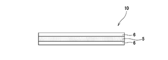
- FIG. 6 is a cross-sectional view showing an example of a single-layer phosphor sheet.
- FIG. 7 is a cross-sectional view showing an example of a two-layer phosphor sheet.
- FIG. 8 is a cross-sectional view showing an example of a single-layer phosphor sheet laminated with a sealing film.
- FIG. 9 is a cross-sectional view showing an example of a two-layer phosphor sheet laminated with a sealing film.
- FIG. 10 is a cross-sectional view showing an example of a sealing film.
- FIG. 11 is a cross-sectional view showing an example of a white light source according to an embodiment of the present invention.
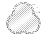
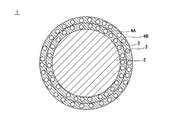
- FIG. 12 is a plan view showing an example of a lighting device according to an embodiment of the present invention.
- FIG. 13 is a cross-sectional view illustrating an example of a lighting device according to an embodiment of the present invention.
- FIG. 14 is a cross-sectional view showing an example of a single-layer phosphor sheet sealed with a sealing film.
- the coated phosphor in the present embodiment is coated with a silicon dioxide film. Thereby, the penetration
- FIG. 1 is a cross-sectional view showing a coated phosphor in which a sulfide phosphor is coated with a silicon dioxide film containing a metal oxide powder.
- a sulfide phosphor 2 is covered with a silicon dioxide film 4 containing a metal oxide powder 3.
- the sulfur-based gas released from the sulfide phosphor 2 by hydrolysis of the sulfide phosphor 2 is Adsorbed on the metal oxide powder 3. Therefore, for example, release of sulfur-based gas from the sulfide phosphor 2 can be suppressed under high temperature and high humidity. Therefore, for example, it is possible to prevent the electrodes and the like from being corroded in the electronic material system, resulting in deterioration of conductivity.
- the sulfide phosphor 2 is not particularly limited.
- SrGa2S4: Eu or CaS: Eu is used.
- the metal oxide powder 3 preferably has a particle size of 0.2 ⁇ m or less.
- the ability of the metal oxide powder 3 to adsorb the sulfur-based gas released from the sulfide phosphor 2 by hydrolysis of the sulfide phosphor 2 by setting the particle size of the metal oxide powder 3 to 0.2 ⁇ m or less. Can be kept from becoming scarce. Thereby, discharge
- the amount of the metal oxide powder 3 is preferably 1 part by mass or more and less than 20 parts by mass, preferably 5 parts by mass or more and 10 parts by mass or less with respect to 100 parts by mass of the sulfide phosphor 2. More preferred. By setting the amount of the metal oxide powder 3 to 1 part by mass or more with respect to 100 parts by mass of the sulfide phosphor 2, an effective adsorption action of the metal oxide powder 3 can be obtained. It is possible to prevent the product powder 3 from having a poor ability to adsorb sulfur-based gas.
- the amount of the metal oxide powder 3 is less than 20 parts by mass with respect to 100 parts by mass of the sulfide phosphor 2, the characteristics of the sulfide phosphor 2, such as peak intensity and luminance, are reduced. This can be prevented.
- the silicon dioxide film 4 is formed on the surface of the sulfide phosphor 2 and covers the surface of the sulfide phosphor 2.
- the silicon dioxide film 4 is produced, for example, by hydrolysis (sol-gel method) of alkoxysilane.
- the thickness of the silicon dioxide film 4 is preferably such that the metal oxide powder 3 is covered with the silicon dioxide film 4.
- the thickness of the silicon dioxide film 4 is preferably 50 to 150 nm.
- the sulfide phosphor 2 is released from the sulfide phosphor 2 by hydrolysis of the sulfide phosphor 2.
- Sulfur-based gas is adsorbed on the metal oxide powder 3. Therefore, for example, release of sulfur-based gas from the sulfide phosphor 2 can be suppressed under high temperature and high humidity.
- the sulfide phosphor 2 does not come into contact with water, it is possible to prevent the sulfide phosphor 2 from being deteriorated by hydrolysis. Thereby, it can prevent that the characteristic of sulfide fluorescent substance 2 falls.
- the coated phosphor 1 may be a secondary particle in which two or more primary particles are connected as shown in FIG. Good. Further, as shown in FIGS. 3 to 5, in the coated phosphor 1, the sulfide phosphor 2 is covered with two or more layers of silicon dioxide film 4, and at least one of the silicon dioxide films 4 has a metal Oxide powder 3 may be contained.
- the coated phosphor 1 includes a two-layered silicon dioxide film 4 on a sulfide phosphor 2, that is, a silicon dioxide film 4 A containing a metal oxide powder 3, and a metal oxide powder.
- the silicon dioxide film 4B containing 3 may be coated in this order.
- the coated phosphor 1 includes a silicon dioxide film 4 ⁇ / b> A containing a metal oxide powder 3 and a silica film, that is, a metal oxide powder 3 on a sulfide phosphor 2.
- the silicon dioxide film 4B that has not been formed may be coated in this order. Further, as shown in FIG.
- the coated phosphor 1 includes a silicon dioxide film 4 ⁇ / b> A that does not contain the metal oxide powder 3 and a silicon dioxide that contains the metal oxide powder 3 on the sulfide phosphor 2.
- the film 4B may be coated in this order.
- coated phosphors 1 shown in FIGS. 3 to 5 at least the silicon dioxide film 4B from the viewpoint of more effectively suppressing the release of sulfur-based gas from the sulfide phosphor 2 under high temperature and high humidity, for example.
- the metal oxide powder 3 is preferably shown in FIGS. 3 and 5. That is, the coated phosphor 1 in which the metal oxide powder 3 is contained in the outermost silicon dioxide film 4B is preferable.
- a method for producing a coated phosphor includes a mixing step in which a phosphor, an alkoxysilane, and a catalyst are mixed in a solvent, and the phosphor is coated with a silicon dioxide film formed from the mixed solution.
- the alkoxysilane can be selected from ethoxide, methoxide, isopropoxide and the like, and examples thereof include tetraethoxysilane and tetramethoxysilane.
- the alkoxysilane may be an alkoxysilane oligomer such as polyethyl silicate or a hydrolysis condensate.
- a silane coupling agent having an alkyl group, an amino group, a mercapto group, or the like that does not contribute to the sol-gel reaction, such as an alkylalkoxysilane, may be used.
- the solvent is not particularly limited, and for example, water, an organic solvent, or the like can be used.
- organic solvent alcohol, ether, ketone, polyhydric alcohol and the like can be used.
- alcohol methanol, ethanol, propanol, pentanol and the like can be used.
- polyhydric alcohols ethylene glycol, propylene glycol, diethylene glycol and the like can be used. Moreover, what combined 2 or more types may be used for a solvent.
- the catalyst is for initiating hydrolysis or polycondensation reaction of alkoxysilane, and for example, an acidic catalyst or a basic catalyst can be used.
- the acidic catalyst include hydrochloric acid, sulfuric acid, boric acid, nitric acid, perchloric acid, tetrafluoroboric acid, hexafluoroarsenic acid, hydrobromic acid, acetic acid, oxalic acid, methanesulfonic acid and the like.
- the basic catalyst include alkali metal hydroxides such as sodium hydroxide, ammonia and the like.
- two or more of these acidic catalysts and basic catalysts may be used in combination.
- the amount of the metal oxide powder is preferably 1 part by mass or more and 20 parts by mass or less with respect to 100 parts by mass of the sulfide phosphor.
- An effective adsorption action of the metal oxide powder can be obtained by blending 1 part by mass or more of the metal oxide powder with respect to 100 parts by mass of the sulfide phosphor. Further, by blending 20 parts by mass or less of metal oxide powder with respect to 100 parts by mass of sulfide phosphor, it is possible to prevent the characteristics of the sulfide phosphor, such as peak intensity and luminance, from being lowered. be able to.
- the mixed phosphor in which the phosphor and alkoxysilane are mixed in a solvent is separated into a solid phase and a liquid phase, whereby a coated phosphor that is a solid phase can be obtained from the mixture.
- a mixed solution is separated into a solid phase and a liquid phase using a suction filter, the separated solid phase is dried, a sample obtained by drying is crushed, and subjected to a firing treatment. Do. Thereby, the coated phosphor in which the phosphor is coated with the silicon dioxide film can be obtained.
- the temperature at which the separated solid phase is dried can be changed according to the solvent used, but is preferably 80 to 110 ° C.
- the time for drying the separated solid phase is preferably 2 hours or longer.
- the temperature for firing the sample is preferably 150 to 250 ° C.
- the time for firing the crushed sample is preferably 8 hours or longer.
- the coated phosphor when the coated phosphor is manufactured, a method of coating the sulfide phosphor with the silicon dioxide film only once, that is, a method of coating the sulfide phosphor with the silicon dioxide film only one layer.
- the silicon dioxide film may be repeatedly coated to coat the phosphor with two or more silicon dioxide films as shown in FIGS.
- the phosphor-containing resin composition in the present embodiment includes a coated phosphor in which the phosphor is coated with a silicon dioxide film, a polymerizable compound, and a polymerization initiator, and at least a sulfide phosphor among the phosphors. Is coated with a silicon dioxide film containing metal oxide powder.
- a red phosphor having a red fluorescence peak with a wavelength of 590 nm to 620 nm by irradiation with blue excitation light and a green fluorescence having a green fluorescence peak with a wavelength of 530 nm to 550 nm by irradiation with blue excitation light It is preferable to use a phosphor mixed with the body.
- red phosphor examples include CaS: Eu, (BaSr) 3 SiO 5 : Eu
- green phosphor examples include inorganic phosphors represented by the following general formula (1).
- M is any one of Ca, Mg, and Ba, and satisfies 0 ⁇ x ⁇ 1 and 0 ⁇ y ⁇ 0.05.
- Specific examples of the green phosphor include SrGa 2 S 4 : Eu.
- a preferred combination in the present embodiment is a mixed phosphor of (BaSr) 3 SiO 5 : Eu that emits red fluorescence and SrGa 2 S 4 : Eu that emits green fluorescence.
- the amount is preferably 1 to 10 parts by mass, more preferably 3 to 6 parts by mass with respect to 100 parts by mass of the resin composition for film formation.
- the polymerizable compound preferably contains a photocurable acrylate. Since the photocurable acrylate has an ester group exhibiting a moisture capturing ability, it is possible to capture more moisture that has entered the phosphor sheet, and to further prevent deterioration of the phosphor due to moisture. Moreover, according to the photocurable acrylate, a phosphor sheet having a small chromaticity shift due to deterioration can be obtained.
- photo-curable acrylates examples include urethane (meth) acrylate, polyester (meth) acrylate, and epoxy acrylate.
- urethane (meth) acrylate can be preferably used from the viewpoint of heat resistance.
- urethane (meth) acrylate a reaction product of a polyol (preferably polyether polyol, polyolefin polyol, polyester polyol or polycarbonate polyol) and a diisocyanate compound (preferably isophorone diisocyanate) is used as a hydroxyalkyl (meth) acrylate. (Preferably, esterified with 21-hydroxypropyl acrylate).
- a polyol preferably polyether polyol, polyolefin polyol, polyester polyol or polycarbonate polyol
- a diisocyanate compound preferably isophorone diisocyanate
- the content of urethane (meth) acrylate is too small, the adhesiveness tends to decrease. Therefore, it is preferable that at least 10 parts by mass is contained in 100 parts by mass of the photocurable acrylate, and at least 30 parts by mass is contained. More preferably.
- the polymerization initiator is preferably a photopolymerization initiator.
- the photopolymerization initiator include radical polymerization initiators such as alkylphenone photopolymerization initiators, acylphosphine oxide photopolymerization initiators, titanocene photopolymerization initiators, oxime ester polymerization initiators, and oxyphenyl acetate esters.
- a cationic polymerization initiator for example, a diazonium polymerization initiator, an iodonium polymerization initiator, a sulphonium polymerization initiator, and the like.
- the amount of these polymerization initiators used is preferably 0.1 to 10 parts by mass, more preferably 1 to 10 parts by mass with respect to 100 parts by mass of the polymerizable compound.
- the phosphor-containing resin composition may be blended with other light-transmitting compounds such as (meth) acrylic monomers and oligomers, coloring pigments and the like, as long as the effects of the present invention are not impaired. it can.
- FIG. 6 is a cross-sectional view of a phosphor sheet according to an embodiment of the present invention.
- a phosphor layer 5 that emits fluorescence when irradiated with excitation light is a single layer sandwiched between a pair of transparent substrates 6, and the phosphor layer 5 is formed from the phosphor-containing resin composition described above. It has been done.
- FIG. 7 is a cross-sectional view of a phosphor sheet having two phosphor layers.
- the phosphor sheet 10 shown in FIG. 6 shows an example in which the phosphor layer 5 is a single layer, but as shown in FIG. 7, two phosphor layers 5 a and 5 b are laminated via a transparent separator 7.
- a laminated phosphor layer 20 having a two-layer structure may be used.
- This phosphor sheet 11 is also sandwiched between a pair of transparent base materials 6a and 6b, similarly to the phosphor sheet 10 shown in FIG.
- one of the phosphor layers 5a and 5b emits red light containing an oxide phosphor (preferably (BaSr) 3 SiO 5 : Eu) having a red fluorescence peak with a wavelength of 590 to 620 nm when irradiated with blue excitation light.
- an oxide phosphor preferably (BaSr) 3 SiO 5 : Eu
- the other is a porous phosphor containing a sulfur-containing phosphor (preferably SrGa 2 S 4 : Eu) having a green fluorescence peak with a wavelength of 530 to 550 nm when irradiated with blue excitation light, and zinc. It is preferable to form from the fluorescent substance containing resin composition containing a crystalline silicate.
- a sulfur-containing phosphor preferably SrGa 2 S 4 : Eu
- the thickness of the phosphor layers 5, 5a, 5b is too thin, the absolute amount of the phosphor is correspondingly reduced, so that sufficient light emission intensity cannot be obtained. On the other hand, if the thickness is too thick, target chromaticity is obtained. Therefore, the thickness is preferably 20 to 150 ⁇ m, more preferably 60 to 120 ⁇ m.
- thermoplastic resin film having a thickness of 10 to 100 ⁇ m a heat or a photocurable resin film can be used.
- examples thereof include a polyester film, a polyamide film, a polyimide film, a polysulfone film, a triacetyl cellulose film, and a polyolefin film.
- the surfaces of these films may be subjected to corona discharge treatment, silane coupling agent treatment, or the like, if necessary.
- the phosphor sheets 10 and 11 shown in FIGS. 6 and 7 are sandwiched between two sealing films 30a and 30b from both sides.
- the phosphor is coated with a silicon dioxide film, and at least the sulfide phosphor of the phosphor is coated with the silicon dioxide film containing the metal oxide powder, as shown in FIGS. Even if the end portion of the phosphor layer is exposed, it is possible to prevent the release of the sulfur-based gas and to further reduce the chromaticity shift.
- the phosphor layer may be a phosphor sheet having an exposed portion between a pair of transparent base materials, it is not necessary to perform a phosphor layer sealing process, and the manufacturing cost of the phosphor sheet can be reduced. It becomes.
- the phosphor sheets 10 and 11 are sealed from both sides with the two sealing films 30a and 30b, the outer circumferences of the two sealing films 30a and 30b and the phosphor sheets 10 and 11 are maintained. It may be sealed with a surrounding frame. By sealing in this way, since the side surfaces of the phosphor sheets 10 and 11 are not exposed, it is possible to further prevent moisture from entering the phosphor layers 5, 5 a and 5 b.
- FIG. 10 is a cross-sectional view showing an example of a sealing film.
- a base film 31 having an adhesive layer 32 formed can be used.
- a silicon oxide layer 33 having a thickness of 5 to 20 nm is formed on the back surface of the base film 31 on the adhesive layer 32 side or the opposite surface by a vapor deposition method or the like. May be.
- the surface protective film 34 may be laminated on the silicon oxide layer 33 via an adhesive layer (not shown).
- the base film 31 and the surface protective film 34 can be used by appropriately selecting from the films exemplified for the transparent substrates 6a and 6b and the transparent separator 7 already described.
- an adhesive layer at the time of laminating the base film 31 and the surface protective film 34 it can be appropriately selected from known adhesives such as urethane adhesives and acrylic adhesives.
- the thickness of the adhesive layer is usually 10 to 50 ⁇ m.
- a single-layer phosphor sheet 10 shown in FIG. 6 forms a phosphor layer 1 by forming a phosphor-containing resin composition on a transparent substrate 6 by a conventional method, and another transparent substrate 6 is formed thereon. It can manufacture by laminating
- the photocurable compound contained in the phosphor layer 5 needs to be photocured (polymerized) by irradiating active energy rays such as ultraviolet rays, for example.
- active energy rays such as ultraviolet rays
- the photocurable compound is directly applied to the phosphor layer 5. You may irradiate an active energy ray, or you may irradiate an active energy ray through the transparent base material 6 or a sealing film.
- the phosphor-containing resin composition is formed on the transparent substrate 6a by a conventional method to form the phosphor layer 5a, and the transparent separator 7 is laminated thereon. Furthermore, another phosphor-containing resin composition containing a phosphor different from the phosphor-containing resin composition is formed by a conventional method to form a phosphor layer 5b, and a transparent substrate 6b is laminated thereon. Can be manufactured. Furthermore, the phosphor sheet 13 having the structure shown in FIG. 9 can be manufactured by sandwiching both surfaces of the phosphor sheet 12 with the sealing films 30a and 30b so that the adhesive layer 32 is on the inner side and thermocompressing the whole. it can.
- the photopolymerizable inclusions contained in the phosphor layers 5a and 5b need to be photocured (polymerized) by irradiating active energy rays such as ultraviolet rays, for example.
- the phosphor layer 5a , 5b may be irradiated with a direct active energy line, or may be irradiated with an active energy ray through the transparent substrates 6a, 6b, the transparent separator 7 and / or the sealing films 30A, 30b. .
- the phosphor-containing resin composition and the phosphor sheet described above can be applied to, for example, a white light source and a lighting device.
- FIG. 11 is a cross-sectional view showing an example of a white light source.
- the white light source 40 has a blue light emitting element 43 on a pad portion 42 formed on an element substrate 41. Electrodes 44 and 45 for supplying electric power for driving the blue light emitting element 43 are formed on the element substrate 41 so as to maintain insulation. The electrodes 44 and 45 are, for example, connected to the blue light emitting element by lead wires 46 and 47, respectively. 43.
- a resin layer 48 is provided around the blue light emitting element 43, and an opening 49 opening on the blue light emitting element 43 is formed in the resin layer 48.
- the opening 49 is formed on an inclined surface whose opening area is widened in the light emitting direction of the blue light emitting element 43, and the reflective film 20 is formed on the inclined surface. That is, the resin layer 48 having the mortar-shaped opening 49 is covered with the reflective film 50 of the opening 49 and the blue light emitting element 43 is disposed on the bottom surface of the opening 49.
- the kneaded material 51 which knead
- a porous silicate containing zinc, a sulfide phosphor having a green fluorescence peak by irradiation with blue excitation light, and a red phosphor having a red fluorescence peak by irradiation with blue excitation light By using a phosphor-containing resin composition containing a polymerizable compound and a polymerization initiator, it is possible to suppress corrosion of the electrodes of the LED element due to sulfur-based gas generated by the deterioration of the sulfide phosphor. it can.
- FIG. 12 is a front view illustrating an example of a lighting device.
- a plurality of white light sources 40 described with reference to FIG. 11 are arranged on the illumination substrate 43.
- the arrangement example may be, for example, a square lattice arrangement as shown in FIG. 12 (A), or an arrangement shifted by 1 ⁇ 2 pitch, for example, every other row as shown in FIG. 12 (B).
- the shifting pitch is not limited to 1/2, and may be 1/3 pitch or 1/4 pitch. Furthermore, you may shift every 1 line or every several lines (for example, 2 lines).
- every other column is shifted by, for example, 1 ⁇ 2 pitch.
- the shifting pitch is not limited to 1/2, and may be 1/3 pitch or 1/4 pitch. Further, it may be shifted every line or every plural lines (for example, 2 lines). That is, how to shift the white light source 10 is not limited.
- the white light source 40 has the same configuration as that described with reference to FIG. That is, the white light source 40 has a kneaded material 51 obtained by kneading a red phosphor and a green phosphor in a transparent resin on the blue light emitting element 43.
- the phosphor-containing resin composition described above is used for the kneaded material 51.
- the illumination device 60 is equivalent to surface light emission because a plurality of white light sources 40 substantially equivalent to point light emission are arranged vertically and horizontally on the illumination substrate 61, so that it is used as a backlight of a liquid crystal display device, for example. be able to.
- the illuminating device 40 can be used for various illuminating devices such as a normal illuminating device, a lighting device for photographing, and a lighting device for construction sites.
- the illumination device 60 uses the white light source 40, it is possible to obtain bright white light with a wide color gamut. For example, when used for a backlight of a liquid crystal display device, pure white with high luminance can be obtained on the display screen, and the quality of the display screen can be improved.
- the lighting device 70 includes a light emitting structure 71 in which a blue light emitting element is covered with a convex surface-shaped transparent resin, a substrate 72 on which the light emitting structure 71 is two-dimensionally arranged, and diffuses blue light from the blue light emitting element.
- the substrate 72 and the phosphor sheet 74 are spaced apart by about 10 to 50 mm, and the lighting device 70 constitutes a so-called remote phosphor structure.
- the gap between the substrate 72 and the phosphor sheet 74 is held by a plurality of support pillars and reflectors, and is provided so that the support pillars and reflectors surround the space formed by the substrate 72 and the phosphor sheet 74 in all directions. .
- the light emitting structure 71 constitutes a so-called LED package having, for example, an InGaN blue LED (Light Emitting Diode) chip as a blue light emitting element.
- LED package having, for example, an InGaN blue LED (Light Emitting Diode) chip as a blue light emitting element.
- the substrate 72 is made of a glass cloth base material using a resin such as phenol, epoxy, polyimide, polyester, bismaleimide triazine, allylated polyphenylene oxide.
- the light emitting structures 71 are two-dimensionally arranged corresponding to the entire surface of the phosphor sheet 74 at equal intervals with a predetermined pitch. Moreover, you may perform a reflection process to the mounting surface of the light emission structure 71 on the board
- the diffusion plate 73 diffuses the radiated light from the light emitting structure 71 over a wide range so that the shape of the light source becomes invisible.
- the diffusing plate 71 one having a total light transmittance of 20% or more and 80% or less is used.
- the phosphor sheet 74 having the structure shown in FIGS. 6 to 9 can be used. That is, a phosphor layer is formed using a phosphor-containing resin composition containing a porous silicate containing zinc, a sulfide phosphor, a polymerizable compound, and a polymerization initiator. Thereby, corrosion of the electrode of the LED element etc. by the sulfur type gas generated by deterioration of sulfide fluorescent substance can be controlled.
- the optical film 75 is composed of, for example, a reflective polarizing film, a lens film, a diffusion film, etc. for improving the visibility of the liquid crystal display device.
- the lens film is an optical film in which minute lenses are arrayed on one surface, and is for increasing the directivity of diffused light in the front direction and increasing the luminance.
- the phosphor contains a coated phosphor coated with a silicon dioxide film, a polymerizable compound, and a polymerization initiator, and at least the sulfide phosphor of the phosphor comprises a metal oxide powder.
- Example> Examples of the present invention will be described below.
- a phosphor sheet having a phosphor layer in which a sulfide phosphor is dispersed in a UV curable acrylic resin is prepared, the luminance and CIE chromaticity of the phosphor sheet are measured, and the chromaticity deviation is evaluated. did.
- production of the sulfur type gas of a fluorescent substance sheet was evaluated.
- the present invention is not limited to these examples.
- the measurement of the brightness and CIE chromaticity of the phosphor sheet, the evaluation of the chromaticity deviation of the phosphor sheet, and the presence or absence of sulfur-based gas generation in the phosphor sheet were measured and evaluated as follows.
- a silver piece test was conducted as an indicator of sulfur gas release. Polishing a piece of silver with a diameter of 15 mm and a thickness of 2 mm (silver bullion (purity 99.95% or more) specified in JIS H 2141 “silver bullion”) with a metal abrasive (Pical, manufactured by Nippon Abrasives Co., Ltd.) And ultrasonically cleaned in acetone. The silver piece after ultrasonic cleaning was attached to the back of the lid of a sealed bottle (100 ml glass weighing bottle) with double-sided tape, and a phosphor sheet (2 cm ⁇ 4 cm) was placed on the bottom inside the sealed bottle.
- Example 1 Into a resin container (PE), 10 g of red phosphor ((Ba, Sr) 3 SiO 6 : Eu), 80 g of ethanol, 5 g of pure water, and 6 g of 28% ammonia water are added, and a magnetic stirrer is added at 40 ° C. After stirring for 10 minutes in a constant temperature bath, 5 g of tetraethoxysilane and 35 g of ethanol were added. Stirring was carried out for 3 hours with the time when the addition was completed as 0 minutes. After the stirring, suction filtration was performed using a vacuum pump, and the collected sample was transferred to a beaker, washed with water or ethanol, and then filtered again to collect the sample. The collected sample was dried at 85 ° C. for 2 hours and baked at 200 ° C. for 8 hours to obtain a coated red phosphor in which the phosphor was coated with a silicon dioxide film.
- PE resin container
- a coating resin composition for film formation containing a photocurable urethane methacrylate (Aronix 1600M, manufactured by Toa Gosei Co., Ltd.) and a photopolymerization initiator (Darocur 1173, manufactured by Nagase Sangyo Co., Ltd.) is coated with 9.0 wt% of the above coated red phosphor. % And 4.5 wt% of the above-mentioned coated green phosphor were uniformly dispersed to obtain a phosphor-containing resin composition.
- the phosphor-containing resin composition is applied onto the first polyethylene terephthalate film so as to have a dry height of 75 ⁇ m, irradiated with ultraviolet rays (7000 mJ / cm 2 ) to polymerize urethane acrylate, and on this phosphor layer.
- the 2nd polyethylene terephthalate film was laminated
- Example 1 A phosphor sheet was obtained in the same manner as in Example 1 except that the green phosphor was used without being coated and was sealed by providing a frame 131 at the end of the phosphor layer 105 as shown in FIG. .
- the relative value of the chromaticity shift of this phosphor sheet was 1.00, and the evaluation of generation of sulfur-based gas was ⁇ .
- Example 2 A phosphor sheet was obtained in the same manner as in Example 1 except that the green phosphor was used without being coated. The relative value of the chromaticity shift of this phosphor sheet was 1.00, and the evaluation of generation of sulfur-based gas was x.
- Example 3 A phosphor sheet was obtained in the same manner as in Example 1 except that zinc oxide powder was not added in the coating treatment of the green phosphor. The relative value of the chromaticity shift of this phosphor sheet was 1.20, and the evaluation of generation of sulfur-based gas was ⁇ .
- Table 1 shows the measurement and evaluation results of Example 1 and Comparative Examples 1 to 3.
- Comparative Example 1 and Comparative Example 2 shows that the release of sulfur-based gas can be suppressed by sealing the end of the phosphor layer. Further, comparing Comparative Example 2 and Comparative Example 3, it can be seen that the release of sulfur-based gas can be suppressed by covering the sulfide phosphor with a silicon dioxide film. Further, when Example 1 and Comparative Example 3 are compared, the release of sulfur-based gas can be sufficiently suppressed by covering the sulfide phosphor with a silicon dioxide film containing zinc oxide powder, and further, chromaticity It can be seen that the deviation can be reduced.
- the phosphor is coated with a silicon dioxide film, and at least the sulfide phosphor among the phosphors is coated with the silicon dioxide film containing the metal oxide powder, whereby the end of the phosphor layer Even with the phosphor sheet exposed, the release of sulfur-based gas can be prevented and the chromaticity shift can be further reduced. For this reason, it is not necessary to perform the sealing process of the phosphor layer, and the manufacturing cost of the phosphor sheet can be reduced.
- SYMBOLS 1 Coated fluorescent substance 2 Sulfide fluorescent substance, 3 Metal oxide powder, 4 Silicon dioxide film, 5, 5a, 5b Phosphor layer, 6, 6a, 6b Transparent base material, 7 Transparent separator 10, 11, 12, 13 phosphor sheet, 20 laminated phosphor layer, 30a, 30b sealing film, 31 base film, 32 adhesive layer, 33 silicon oxide layer, 34 surface protective film, 40 white light source, 41 element substrate, 42 pad portion, 43 blue Light emitting element, 44 electrode, 45 electrode, 46 lead wire, 47 lead wire, 48 resin layer, 49 opening, 50 reflective film, 51 kneaded product, 60 lighting device, 61 lighting substrate, 70 lighting device, 71 light emitting structure, 72 substrate, 73 diffusion plate, 74 phosphor sheet, 75 optical film
Priority Applications (4)
| Application Number | Priority Date | Filing Date | Title |
|---|---|---|---|
| CN201380039337.7A CN104471024A (zh) | 2012-07-25 | 2013-07-16 | 荧光体片 |
| KR1020157003913A KR102120951B1 (ko) | 2012-07-25 | 2013-07-16 | 형광체 시트 |
| EP13823548.6A EP2878646B1 (de) | 2012-07-25 | 2013-07-16 | Phosphorschicht |
| US14/605,356 US9850427B2 (en) | 2012-07-25 | 2015-01-26 | Phosphor sheet |
Applications Claiming Priority (2)
| Application Number | Priority Date | Filing Date | Title |
|---|---|---|---|
| JP2012165056A JP6038524B2 (ja) | 2012-07-25 | 2012-07-25 | 蛍光体シート |
| JP2012-165056 | 2012-07-25 |
Related Child Applications (1)
| Application Number | Title | Priority Date | Filing Date |
|---|---|---|---|
| US14/605,356 Continuation US9850427B2 (en) | 2012-07-25 | 2015-01-26 | Phosphor sheet |
Publications (1)
| Publication Number | Publication Date |
|---|---|
| WO2014017334A1 true WO2014017334A1 (ja) | 2014-01-30 |
Family
ID=49997148
Family Applications (1)
| Application Number | Title | Priority Date | Filing Date |
|---|---|---|---|
| PCT/JP2013/069289 WO2014017334A1 (ja) | 2012-07-25 | 2013-07-16 | 蛍光体シート |
Country Status (7)
| Country | Link |
|---|---|
| US (1) | US9850427B2 (de) |
| EP (1) | EP2878646B1 (de) |
| JP (1) | JP6038524B2 (de) |
| KR (1) | KR102120951B1 (de) |
| CN (1) | CN104471024A (de) |
| TW (2) | TWI596189B (de) |
| WO (1) | WO2014017334A1 (de) |
Cited By (4)
| Publication number | Priority date | Publication date | Assignee | Title |
|---|---|---|---|---|
| WO2015146231A1 (ja) * | 2014-03-27 | 2015-10-01 | 三井金属鉱業株式会社 | 蛍光体及びその用途 |
| WO2015185296A1 (de) * | 2014-06-03 | 2015-12-10 | Osram Gmbh | Lichtkonversionsvorrichtung und verfahren zum seiner herstellung |
| JP2021533227A (ja) * | 2018-08-03 | 2021-12-02 | ボード オブ リージェンツ, ザ ユニバーシティ オブ テキサス システムBoard Of Regents, The University Of Texas System | ポリマー性マトリックスにおける蛍光体の分散を増進させるための方法及び組成物 |
| US11393949B2 (en) | 2014-05-27 | 2022-07-19 | Osram Opto Semiconductors Gmbh | Semiconductor component and illumination device |
Families Citing this family (24)
| Publication number | Priority date | Publication date | Assignee | Title |
|---|---|---|---|---|
| US10655792B2 (en) * | 2014-09-28 | 2020-05-19 | Zhejiang Super Lighting Electric Appliance Co., Ltd. | LED bulb lamp |
| WO2015138495A1 (en) * | 2014-03-11 | 2015-09-17 | Osram Sylvania Inc. | Light converter assemblies with enhanced heat dissipation |
| DE102015113692A1 (de) * | 2014-09-11 | 2016-03-24 | Panasonic Intellectual Property Management Co., Ltd. | Wellenlängen-Umwandlungs-Element, Licht-emittierende Vorrichtung, Projektor und Verfahren zur Herstellung eines Wellenlängen-Umwandlungs-Elements |
| US11543083B2 (en) | 2014-09-28 | 2023-01-03 | Zhejiang Super Lighting Electric Appliance Co., Ltd | LED filament and LED light bulb |
| US11690148B2 (en) | 2014-09-28 | 2023-06-27 | Zhejiang Super Lighting Electric Appliance Co., Ltd. | LED filament and LED light bulb |
| US11421827B2 (en) | 2015-06-19 | 2022-08-23 | Zhejiang Super Lighting Electric Appliance Co., Ltd | LED filament and LED light bulb |
| US11686436B2 (en) | 2014-09-28 | 2023-06-27 | Zhejiang Super Lighting Electric Appliance Co., Ltd | LED filament and light bulb using LED filament |
| US11085591B2 (en) | 2014-09-28 | 2021-08-10 | Zhejiang Super Lighting Electric Appliance Co., Ltd | LED light bulb with curved filament |
| US11525547B2 (en) | 2014-09-28 | 2022-12-13 | Zhejiang Super Lighting Electric Appliance Co., Ltd | LED light bulb with curved filament |
| US11073248B2 (en) | 2014-09-28 | 2021-07-27 | Zhejiang Super Lighting Electric Appliance Co., Ltd. | LED bulb lamp |
| JP6657735B2 (ja) * | 2014-10-07 | 2020-03-04 | 日亜化学工業株式会社 | 発光装置 |
| US10490711B2 (en) | 2014-10-07 | 2019-11-26 | Nichia Corporation | Light emitting device |
| JP6401994B2 (ja) * | 2014-10-08 | 2018-10-10 | エルジー ディスプレイ カンパニー リミテッド | 液晶表示装置 |
| EP3029515B1 (de) * | 2014-12-03 | 2019-03-20 | Samsung Electronics Co., Ltd. | Weisslichtemittierende vorrichtung und anzeigevorrichtung damit |
| CN104633551A (zh) * | 2015-03-03 | 2015-05-20 | 深圳市华星光电技术有限公司 | 白光led、背光模块及液晶显示装置 |
| JP2018056512A (ja) * | 2016-09-30 | 2018-04-05 | デクセリアルズ株式会社 | 発光装置、及び発光装置の製造方法 |
| JP2020500244A (ja) * | 2016-10-31 | 2020-01-09 | インテマティックス・コーポレーションIntematix Corporation | コーティング付き狭帯域緑色蛍光体 |
| JP6949806B2 (ja) * | 2017-11-30 | 2021-10-13 | デクセリアルズ株式会社 | 緑色蛍光体、蛍光体シート、及び発光装置 |
| WO2019107285A1 (ja) * | 2017-11-30 | 2019-06-06 | デクセリアルズ株式会社 | 緑色蛍光体、蛍光体シート、及び発光装置 |
| CN108084736B (zh) * | 2017-12-19 | 2020-07-24 | 包头中科世纪科技有限责任公司 | 一种简单无污染处理稀土硫化物颜料的工艺 |
| TWI677109B (zh) * | 2018-02-02 | 2019-11-11 | 國立臺灣大學 | 抬頭顯示器、發光薄膜與其製法 |
| JP7161100B2 (ja) * | 2018-09-25 | 2022-10-26 | 日亜化学工業株式会社 | 発光装置及びその製造方法 |
| KR20210012514A (ko) * | 2019-07-25 | 2021-02-03 | 엘지이노텍 주식회사 | 광학 레진 및 이를 갖는 조명장치 |
| US20230236063A1 (en) * | 2022-01-24 | 2023-07-27 | Analytik Jena Us Llc | Light conversion device with high uniformity |
Citations (16)
| Publication number | Priority date | Publication date | Assignee | Title |
|---|---|---|---|---|
| JPH0665570A (ja) * | 1992-06-17 | 1994-03-08 | Toshiba Corp | 電場発光蛍光体およびその製造方法 |
| JPH09272866A (ja) * | 1996-04-03 | 1997-10-21 | Toshiba Corp | 電場発光蛍光体およびその製造方法 |
| JP2005108635A (ja) | 2003-09-30 | 2005-04-21 | Sony Corp | 面発光装置および液晶表示装置 |
| JP2006188700A (ja) * | 2005-01-03 | 2006-07-20 | Samsung Electro Mech Co Ltd | 硫化物系蛍光体の被膜形成方法及び表面コーティング硫化物系蛍光体 |
| JP2006265326A (ja) * | 2005-03-23 | 2006-10-05 | Stanley Electric Co Ltd | 蛍光体、その製造方法、及び発光装置 |
| JP2007005098A (ja) | 2005-06-23 | 2007-01-11 | Seiko Instruments Inc | 蛍光体フィルム、それを用いた照明装置ならびに表示装置 |
| JP2007023221A (ja) | 2005-07-20 | 2007-02-01 | Bando Chem Ind Ltd | 被覆発光体およびその利用 |
| JP2007091874A (ja) * | 2005-09-28 | 2007-04-12 | Toda Kogyo Corp | 耐湿性蛍光体粒子粉末及び該耐湿性蛍光体粒子粉末を用いたled素子または分散型el素子 |
| JP2008031190A (ja) | 2006-07-26 | 2008-02-14 | Shin Etsu Chem Co Ltd | Led用蛍光物質入り硬化性シリコーン組成物およびその組成物を使用するled発光装置。 |
| JP2008041706A (ja) | 2006-08-01 | 2008-02-21 | Dainippon Printing Co Ltd | 発光装置および白色変換シート |
| JP2009526089A (ja) * | 2005-12-01 | 2009-07-16 | サーノフ コーポレーション | 湿気保護蛍光体およびled照明デバイス |
| JP2009283438A (ja) | 2007-12-07 | 2009-12-03 | Sony Corp | 照明装置、表示装置、照明装置の製造方法 |
| JP2009293441A (ja) | 2008-06-03 | 2009-12-17 | Toyota Motor Corp | 内燃機関の排気ガス再循環装置 |
| JP2011195727A (ja) * | 2010-03-19 | 2011-10-06 | Panasonic Electric Works Co Ltd | 波長変換粒子、波長変換部材及び発光装置 |
| WO2012077656A1 (ja) * | 2010-12-09 | 2012-06-14 | 三井金属鉱業株式会社 | ZnO化合物被覆硫黄含有蛍光体 |
| WO2013021990A1 (ja) * | 2011-08-11 | 2013-02-14 | 三井金属鉱業株式会社 | 赤色蛍光体及び発光素子 |
Family Cites Families (10)
| Publication number | Priority date | Publication date | Assignee | Title |
|---|---|---|---|---|
| DE69606215T2 (de) * | 1995-04-20 | 2000-09-07 | Matsushita Electric Ind Co Ltd | Herstellungsverfahren einer Plasmaanzeigetafel |
| JP2004161808A (ja) * | 2002-11-08 | 2004-06-10 | Nichia Chem Ind Ltd | 窒化物系蛍光シート、発光装置および窒化物系蛍光膜の製造方法 |
| US7839072B2 (en) * | 2006-05-24 | 2010-11-23 | Citizen Electronics Co., Ltd. | Translucent laminate sheet and light-emitting device using the translucent laminate sheet |
| KR101414243B1 (ko) * | 2007-03-30 | 2014-07-14 | 서울반도체 주식회사 | 황화물 형광체 코팅 방법 및 코팅된 황화물 형광체를채택한 발광 소자 |
| CN201462686U (zh) * | 2009-02-18 | 2010-05-12 | 绎立锐光科技开发(深圳)有限公司 | 光波长转换材料的封装结构及led光源 |
| CN101805602B (zh) * | 2009-02-18 | 2014-03-26 | 深圳市绎立锐光科技开发有限公司 | 光波长转换材料的封装方法及结构 |
| JP5249283B2 (ja) * | 2010-05-10 | 2013-07-31 | デクセリアルズ株式会社 | 緑色発光蛍光体粒子及びその製造方法、並びに、色変換シート、発光装置及び画像表示装置組立体 |
| EP2730616B1 (de) * | 2011-07-05 | 2019-04-17 | Dexerials Corporation | Phosphoreszenzfolie bildende harzzusammensetzung |
| JP5373859B2 (ja) * | 2011-07-05 | 2013-12-18 | デクセリアルズ株式会社 | 照明装置 |
| JP2013119581A (ja) * | 2011-12-07 | 2013-06-17 | Dexerials Corp | 被覆蛍光体及び被覆蛍光体の製造方法 |
-
2012
- 2012-07-25 JP JP2012165056A patent/JP6038524B2/ja active Active
-
2013
- 2013-07-16 TW TW102125365A patent/TWI596189B/zh active
- 2013-07-16 WO PCT/JP2013/069289 patent/WO2014017334A1/ja active Application Filing
- 2013-07-16 CN CN201380039337.7A patent/CN104471024A/zh active Pending
- 2013-07-16 EP EP13823548.6A patent/EP2878646B1/de active Active
- 2013-07-16 TW TW106118004A patent/TWI680180B/zh active
- 2013-07-16 KR KR1020157003913A patent/KR102120951B1/ko active IP Right Grant
-
2015
- 2015-01-26 US US14/605,356 patent/US9850427B2/en active Active
Patent Citations (16)
| Publication number | Priority date | Publication date | Assignee | Title |
|---|---|---|---|---|
| JPH0665570A (ja) * | 1992-06-17 | 1994-03-08 | Toshiba Corp | 電場発光蛍光体およびその製造方法 |
| JPH09272866A (ja) * | 1996-04-03 | 1997-10-21 | Toshiba Corp | 電場発光蛍光体およびその製造方法 |
| JP2005108635A (ja) | 2003-09-30 | 2005-04-21 | Sony Corp | 面発光装置および液晶表示装置 |
| JP2006188700A (ja) * | 2005-01-03 | 2006-07-20 | Samsung Electro Mech Co Ltd | 硫化物系蛍光体の被膜形成方法及び表面コーティング硫化物系蛍光体 |
| JP2006265326A (ja) * | 2005-03-23 | 2006-10-05 | Stanley Electric Co Ltd | 蛍光体、その製造方法、及び発光装置 |
| JP2007005098A (ja) | 2005-06-23 | 2007-01-11 | Seiko Instruments Inc | 蛍光体フィルム、それを用いた照明装置ならびに表示装置 |
| JP2007023221A (ja) | 2005-07-20 | 2007-02-01 | Bando Chem Ind Ltd | 被覆発光体およびその利用 |
| JP2007091874A (ja) * | 2005-09-28 | 2007-04-12 | Toda Kogyo Corp | 耐湿性蛍光体粒子粉末及び該耐湿性蛍光体粒子粉末を用いたled素子または分散型el素子 |
| JP2009526089A (ja) * | 2005-12-01 | 2009-07-16 | サーノフ コーポレーション | 湿気保護蛍光体およびled照明デバイス |
| JP2008031190A (ja) | 2006-07-26 | 2008-02-14 | Shin Etsu Chem Co Ltd | Led用蛍光物質入り硬化性シリコーン組成物およびその組成物を使用するled発光装置。 |
| JP2008041706A (ja) | 2006-08-01 | 2008-02-21 | Dainippon Printing Co Ltd | 発光装置および白色変換シート |
| JP2009283438A (ja) | 2007-12-07 | 2009-12-03 | Sony Corp | 照明装置、表示装置、照明装置の製造方法 |
| JP2009293441A (ja) | 2008-06-03 | 2009-12-17 | Toyota Motor Corp | 内燃機関の排気ガス再循環装置 |
| JP2011195727A (ja) * | 2010-03-19 | 2011-10-06 | Panasonic Electric Works Co Ltd | 波長変換粒子、波長変換部材及び発光装置 |
| WO2012077656A1 (ja) * | 2010-12-09 | 2012-06-14 | 三井金属鉱業株式会社 | ZnO化合物被覆硫黄含有蛍光体 |
| WO2013021990A1 (ja) * | 2011-08-11 | 2013-02-14 | 三井金属鉱業株式会社 | 赤色蛍光体及び発光素子 |
Non-Patent Citations (1)
| Title |
|---|
| See also references of EP2878646A4 |
Cited By (7)
| Publication number | Priority date | Publication date | Assignee | Title |
|---|---|---|---|---|
| WO2015146231A1 (ja) * | 2014-03-27 | 2015-10-01 | 三井金属鉱業株式会社 | 蛍光体及びその用途 |
| JP5796148B1 (ja) * | 2014-03-27 | 2015-10-21 | 三井金属鉱業株式会社 | 蛍光体及びその用途 |
| KR101850755B1 (ko) | 2014-03-27 | 2018-04-23 | 미쓰이금속광업주식회사 | 형광체 및 그 용도 |
| US10550321B2 (en) | 2014-03-27 | 2020-02-04 | Mitsui Mining & Smelting Co., Ltd. | Phosphor and use thereof |
| US11393949B2 (en) | 2014-05-27 | 2022-07-19 | Osram Opto Semiconductors Gmbh | Semiconductor component and illumination device |
| WO2015185296A1 (de) * | 2014-06-03 | 2015-12-10 | Osram Gmbh | Lichtkonversionsvorrichtung und verfahren zum seiner herstellung |
| JP2021533227A (ja) * | 2018-08-03 | 2021-12-02 | ボード オブ リージェンツ, ザ ユニバーシティ オブ テキサス システムBoard Of Regents, The University Of Texas System | ポリマー性マトリックスにおける蛍光体の分散を増進させるための方法及び組成物 |
Also Published As
| Publication number | Publication date |
|---|---|
| US9850427B2 (en) | 2017-12-26 |
| EP2878646B1 (de) | 2017-12-13 |
| CN104471024A (zh) | 2015-03-25 |
| EP2878646A1 (de) | 2015-06-03 |
| KR20150038078A (ko) | 2015-04-08 |
| JP2014024918A (ja) | 2014-02-06 |
| TW201420723A (zh) | 2014-06-01 |
| TWI680180B (zh) | 2019-12-21 |
| JP6038524B2 (ja) | 2016-12-07 |
| US20150197689A1 (en) | 2015-07-16 |
| TWI596189B (zh) | 2017-08-21 |
| KR102120951B1 (ko) | 2020-06-09 |
| TW201732019A (zh) | 2017-09-16 |
| EP2878646A4 (de) | 2016-08-10 |
Similar Documents
| Publication | Publication Date | Title |
|---|---|---|
| JP6038524B2 (ja) | 蛍光体シート | |
| KR101604339B1 (ko) | 광 변환 필름, 이를 포함하는 백라이트 유닛 및 표시장치 | |
| JP4898332B2 (ja) | 表示装置 | |
| JP4931628B2 (ja) | 照明装置及びこれを備える表示装置 | |
| TWI498642B (zh) | 光學件與具有其之顯示裝置以及其製作方法 | |
| WO2015037733A1 (ja) | 波長変換シート及びバックライトユニット | |
| US9540563B2 (en) | Coated phosphor and method for producing coated phosphor | |
| JP5468985B2 (ja) | 照明装置 | |
| KR20160069393A (ko) | 광 변환 복합재의 제조방법, 광 변환 복합재, 이를 포함하는 광 변환 필름, 백라이트 유닛 및 표시장치 | |
| JP2009231273A (ja) | 照明装置及びこれを備える表示装置 | |
| JP2013032515A (ja) | 蛍光体シート形成用樹脂組成物 | |
| KR20180131399A (ko) | 발광 장치 및 발광 장치의 제조 방법 | |
| JP7284373B2 (ja) | 発光装置 | |
| KR20140143060A (ko) | 유기 형광체를 포함하는 광학필름 및 이를 포함하는 백라이트 유닛 | |
| JP2013067710A (ja) | 被覆蛍光体の製造方法、被覆蛍光体及び白色光源 | |
| JP2014024917A (ja) | 蛍光体含有樹脂組成物 | |
| JP2019214741A (ja) | 波長変換部材、蛍光体シート、白色光源装置、及び表示装置 | |
| JP6258418B2 (ja) | 被覆蛍光体の製造方法 | |
| KR101882199B1 (ko) | 광학 부재, 이를 포함하는 표시장치 및 이의 제조방법 | |
| KR20120126396A (ko) | 광학 부재, 이를 포함하는 표시장치 및 이의 제조방법 | |
| KR20130039405A (ko) | 발광 소자 패키지 | |
| JP2016028170A (ja) | 被覆蛍光体の製造方法、被覆蛍光体及び白色光源 | |
| KR20160089303A (ko) | 광 변환 복합재의 제조방법, 광 변환 복합재, 이를 포함하는 광 변환 필름, 백라이트 유닛 및 표시장치 | |
| KR20090098152A (ko) | 형광램프용 형광혼합물, 이를 갖는 형광램프 및 이를 갖는표시장치 |
Legal Events
| Date | Code | Title | Description |
|---|---|---|---|
| 121 | Ep: the epo has been informed by wipo that ep was designated in this application |
Ref document number: 13823548 Country of ref document: EP Kind code of ref document: A1 |
|
| NENP | Non-entry into the national phase |
Ref country code: DE |
|
| ENP | Entry into the national phase |
Ref document number: 20157003913 Country of ref document: KR Kind code of ref document: A |
|
| WWE | Wipo information: entry into national phase |
Ref document number: 2013823548 Country of ref document: EP |