WO2014010371A1 - 化合物太陽電池の製法 - Google Patents
化合物太陽電池の製法 Download PDFInfo
- Publication number
- WO2014010371A1 WO2014010371A1 PCT/JP2013/066546 JP2013066546W WO2014010371A1 WO 2014010371 A1 WO2014010371 A1 WO 2014010371A1 JP 2013066546 W JP2013066546 W JP 2013066546W WO 2014010371 A1 WO2014010371 A1 WO 2014010371A1
- Authority
- WO
- WIPO (PCT)
- Prior art keywords
- vapor deposition
- nozzle
- deposition source
- group
- base material
- Prior art date
- Legal status (The legal status is an assumption and is not a legal conclusion. Google has not performed a legal analysis and makes no representation as to the accuracy of the status listed.)
- Ceased
Links
Images




Classifications
-
- H—ELECTRICITY
- H10—SEMICONDUCTOR DEVICES; ELECTRIC SOLID-STATE DEVICES NOT OTHERWISE PROVIDED FOR
- H10F—INORGANIC SEMICONDUCTOR DEVICES SENSITIVE TO INFRARED RADIATION, LIGHT, ELECTROMAGNETIC RADIATION OF SHORTER WAVELENGTH OR CORPUSCULAR RADIATION
- H10F77/00—Constructional details of devices covered by this subclass
- H10F77/10—Semiconductor bodies
- H10F77/12—Active materials
- H10F77/126—Active materials comprising only Group I-III-VI chalcopyrite materials, e.g. CuInSe2, CuGaSe2 or CuInGaSe2 [CIGS]
-
- C—CHEMISTRY; METALLURGY
- C23—COATING METALLIC MATERIAL; COATING MATERIAL WITH METALLIC MATERIAL; CHEMICAL SURFACE TREATMENT; DIFFUSION TREATMENT OF METALLIC MATERIAL; COATING BY VACUUM EVAPORATION, BY SPUTTERING, BY ION IMPLANTATION OR BY CHEMICAL VAPOUR DEPOSITION, IN GENERAL; INHIBITING CORROSION OF METALLIC MATERIAL OR INCRUSTATION IN GENERAL
- C23C—COATING METALLIC MATERIAL; COATING MATERIAL WITH METALLIC MATERIAL; SURFACE TREATMENT OF METALLIC MATERIAL BY DIFFUSION INTO THE SURFACE, BY CHEMICAL CONVERSION OR SUBSTITUTION; COATING BY VACUUM EVAPORATION, BY SPUTTERING, BY ION IMPLANTATION OR BY CHEMICAL VAPOUR DEPOSITION, IN GENERAL
- C23C14/00—Coating by vacuum evaporation, by sputtering or by ion implantation of the coating forming material
- C23C14/06—Coating by vacuum evaporation, by sputtering or by ion implantation of the coating forming material characterised by the coating material
- C23C14/0623—Sulfides, selenides or tellurides
-
- C—CHEMISTRY; METALLURGY
- C23—COATING METALLIC MATERIAL; COATING MATERIAL WITH METALLIC MATERIAL; CHEMICAL SURFACE TREATMENT; DIFFUSION TREATMENT OF METALLIC MATERIAL; COATING BY VACUUM EVAPORATION, BY SPUTTERING, BY ION IMPLANTATION OR BY CHEMICAL VAPOUR DEPOSITION, IN GENERAL; INHIBITING CORROSION OF METALLIC MATERIAL OR INCRUSTATION IN GENERAL
- C23C—COATING METALLIC MATERIAL; COATING MATERIAL WITH METALLIC MATERIAL; SURFACE TREATMENT OF METALLIC MATERIAL BY DIFFUSION INTO THE SURFACE, BY CHEMICAL CONVERSION OR SUBSTITUTION; COATING BY VACUUM EVAPORATION, BY SPUTTERING, BY ION IMPLANTATION OR BY CHEMICAL VAPOUR DEPOSITION, IN GENERAL
- C23C14/00—Coating by vacuum evaporation, by sputtering or by ion implantation of the coating forming material
- C23C14/22—Coating by vacuum evaporation, by sputtering or by ion implantation of the coating forming material characterised by the process of coating
- C23C14/56—Apparatus specially adapted for continuous coating; Arrangements for maintaining the vacuum, e.g. vacuum locks
- C23C14/562—Apparatus specially adapted for continuous coating; Arrangements for maintaining the vacuum, e.g. vacuum locks for coating elongated substrates
-
- H—ELECTRICITY
- H10—SEMICONDUCTOR DEVICES; ELECTRIC SOLID-STATE DEVICES NOT OTHERWISE PROVIDED FOR
- H10P—GENERIC PROCESSES OR APPARATUS FOR THE MANUFACTURE OR TREATMENT OF DEVICES COVERED BY CLASS H10
- H10P14/00—Formation of materials, e.g. in the shape of layers or pillars
- H10P14/20—Formation of materials, e.g. in the shape of layers or pillars of semiconductor materials
- H10P14/34—Deposited materials, e.g. layers
- H10P14/3402—Deposited materials, e.g. layers characterised by the chemical composition
- H10P14/3436—Deposited materials, e.g. layers characterised by the chemical composition being chalcogenide semiconductor materials not being oxides, e.g. ternary compounds
-
- Y—GENERAL TAGGING OF NEW TECHNOLOGICAL DEVELOPMENTS; GENERAL TAGGING OF CROSS-SECTIONAL TECHNOLOGIES SPANNING OVER SEVERAL SECTIONS OF THE IPC; TECHNICAL SUBJECTS COVERED BY FORMER USPC CROSS-REFERENCE ART COLLECTIONS [XRACs] AND DIGESTS
- Y02—TECHNOLOGIES OR APPLICATIONS FOR MITIGATION OR ADAPTATION AGAINST CLIMATE CHANGE
- Y02E—REDUCTION OF GREENHOUSE GAS [GHG] EMISSIONS, RELATED TO ENERGY GENERATION, TRANSMISSION OR DISTRIBUTION
- Y02E10/00—Energy generation through renewable energy sources
- Y02E10/50—Photovoltaic [PV] energy
- Y02E10/541—CuInSe2 material PV cells
-
- Y—GENERAL TAGGING OF NEW TECHNOLOGICAL DEVELOPMENTS; GENERAL TAGGING OF CROSS-SECTIONAL TECHNOLOGIES SPANNING OVER SEVERAL SECTIONS OF THE IPC; TECHNICAL SUBJECTS COVERED BY FORMER USPC CROSS-REFERENCE ART COLLECTIONS [XRACs] AND DIGESTS
- Y02—TECHNOLOGIES OR APPLICATIONS FOR MITIGATION OR ADAPTATION AGAINST CLIMATE CHANGE
- Y02P—CLIMATE CHANGE MITIGATION TECHNOLOGIES IN THE PRODUCTION OR PROCESSING OF GOODS
- Y02P70/00—Climate change mitigation technologies in the production process for final industrial or consumer products
- Y02P70/50—Manufacturing or production processes characterised by the final manufactured product
Definitions
- a compound solar cell using a CIS or CIGS (hereinafter referred to as “CIGS-based”) compound semiconductor for a light absorption layer has a high conversion efficiency and can be formed into a thin film, and has a conversion efficiency due to light irradiation or the like. It is known to have the advantage of less degradation.
- the compound semiconductor layer has a chalcopyrite structure composed of Group I, Group III, and Group VI elements, it is possible to perform high-efficiency light conversion even with a thin film and to be stable at room temperature. .
- FIG. 1 is a cross-sectional view of a CIGS solar cell obtained according to an embodiment of the present invention.
- This CIGS solar cell has a size of width 20 mm ⁇ length 20 mm ⁇ thickness 53 ⁇ m, a base material 1 (thickness 50 ⁇ m) made of stainless alloy (SUS), and a back electrode layer 2 (thickness 800 nm) made of molybdenum (Mo).
- a compound semiconductor layer (CIGS light absorption layer) 3 (thickness 2 ⁇ m) made of a chalcopyrite compound, a buffer layer 4 (thickness 70 nm) made of ZnO, and a surface electrode layer 5 (thickness 200 nm) made of ITO in this order.
- tungsten (W), chromium (Cr), titanium (Ti), etc. can be used in addition to the Mo. It can also be used by forming in multiple layers.
- the thickness is preferably in the range of 100 to 1000 nm.
- the buffer layer 4 formed on the CIGS light absorption layer is preferably a high-resistance n-type semiconductor so that a pn junction can be formed with the CIGS light absorption layer 3. It may consist of layers. When the buffer layer 4 is composed of a plurality of layers, the pn junction with the CIGS light absorption layer 3 can be improved. As the buffer layer 4, any material other than the above ZnO can be used. For example, CdS, ZnMgO, Zn (O, S), or the like can be used. When the buffer layer 4 is composed of a plurality of layers, the thickness of each layer is preferably in the range of 30 to 200 nm. Even when the buffer layer 4 is a single layer, the thickness is preferably 30 to 200 nm.
- a back electrode layer 2 is formed on the surface of a long substrate 1, and CIGS light absorption is performed on the back electrode layer 2 using a vapor deposition apparatus 6 shown in FIG.
- the buffer layer 4 and the surface electrode layer 5 are laminated on the CIGS light absorption layer 3 in this order. be able to. The manufacturing method will be described in detail below.
- the back electrode layer 2 made of Mo is formed on the surface of the long base material 1 by a sputtering method while running the long base material 1 by the roll-to-roll method.
- the back electrode layer 2 can also be formed by a vapor deposition method in addition to the sputtering method.
- the CIGS light absorption layer 3 is formed on the back electrode layer 2 while the base material 1 (hereinafter referred to as “base material”) on which the back electrode layer 2 is formed is also run in a roll-to-roll manner.
- base material the base material 1
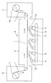
- a vapor deposition apparatus 6 as shown in FIG. 2 is used. This vapor deposition apparatus 6 forms the CIGS light absorption layer 3 with respect to the base material 1 by the vapor deposition chamber 8 for unwinding the base material 1 from the unwinding roll 7 by which the base material 1 was wound, and vapor deposition.
- Vapor deposition chamber 9 and a winding chamber 11 for accommodating a winding roll 10 for winding the substrate 1 on which the CIGS light absorption layer 3 is formed.
- the chambers 8, 9, and 11 are connected by a differential exhaust mechanism for reducing the pressure difference, so that the substrate 1 can be continuously moved between chambers having different pressures. ing.
- the CIGS light absorption layer 3 can be continuously formed on the long base 1 by passing the base 1 through the chambers 8, 9, and 11.
- the vapor deposition chamber 9 is provided with three vapor deposition sources A provided with nozzles 12 for supplying Se (group VI element), and supplies Cu, In and Ga (elements other than group VI elements).
- the vapor deposition source B provided with the supply port to be provided is provided for each element (three in total).
- the supply ports 14 of the respective vapor deposition sources B are arranged at a position 5 to 70 mm away from the base material 1, and the tip opening 13 of the nozzle 12 is connected to the base material 1 from the supply port 14 of the vapor deposition source B. It is arranged at a close position.
- the opening diameter of the nozzle 12 attached to the vapor deposition source A is 10 mm.
- the opening diameter of the nozzle 12 is not limited to this, and is preferably in the range of 1 to 30 mm, and in the range of 5 to 20 mm. More preferably. That is, if the diameter is too large, the distribution of the ejected material will be good, but the ejection pressure of Se will be low, and Se may not be able to sufficiently wrap around Cu, In and Ga. If it is too small, the ejection pressure of Se is improved, but a good distribution cannot be obtained, and compositional unevenness of the Se material in the CIGS light absorption layer 3 may occur.
- heating means for example, heating wire
- this heating means may not be provided.
- the vapor deposition apparatus 6 In order to obtain the CIGS light absorption layer 3 using this vapor deposition apparatus 6, first, it is heated by a heating mechanism (not shown) provided in the vapor deposition chamber 9 so that the temperature of the base material 1 at the time of vapor deposition is 550 ° C. To do. At this time, the temperature of the substrate 1 may become too high due to the heat generated from the vapor deposition sources A and B, and a separate cooling mechanism (not shown) for cooling the substrate 1 is provided in the vapor deposition chamber 9. You may make it provide in. Then, the vapor deposition chamber 9 is set in a vacuum state, the vapor deposition source A (Se material unit) is heated to 350 ° C., the nozzle 12 is heated to 450 ° C.
- a heating mechanism not shown
- each material unit of Cu, In, and Ga arranged as the vapor deposition source B is heated to 1300 ° C., 1100 ° C., and 1100 ° C., respectively, and 60 ° toward the substrate 1 from the supply port 14.
- Se can sufficiently wrap around Cu, In, and Ga even when the substrate 1 and the evaporation sources A and B are close to each other.
- the CIGS light absorption layer 3 having a chalcopyrite structure [Cu (In 1 ⁇ X , Ga x ) Se 2 ] having a desired composition ratio can be obtained on the substrate 1.
- the nozzle 12 of the vapor deposition source A is disposed so that an angle ⁇ 1 formed by the imaginary line I 1 indicating the ejection direction of Se from the tip opening 13 and the substrate 1 is 20 °.
- the arrangement is not limited to this, but it is preferable to arrange the angle ⁇ 1 to be an arbitrary angle in the range of 0 to 30 °.
- the supply port 14 of the vapor deposition source B is arranged so that an angle ⁇ 2 formed by a virtual line I 2 indicating the supply direction of Cu, In, and Ga and the substrate 1 is 60 °.
- the tip opening 13 of the nozzle 12 has a shortest distance L 1 from the surface of the substrate 1 set to 10 mm.
- the present invention is not limited to this, and the shortest distance L 1 is from the surface of the substrate 1 to the evaporation source B. Can be set to any range shorter than the shortest distance L 2 to the supply port 14.
- the shortest distance L 2 is set to 50 mm, but is not limited to this, and can be set to any range of 5 to 70 mm.
- the number can be increased or decreased in consideration of the size of the vapor deposition chamber 9 and the base material 1, the transport speed of the base material 1, and the like.
- the vapor deposition source A and the vapor deposition source B are installed in the ratio of 1: 1, it is not necessarily required. That is, as shown in FIG. 5, when the nozzle 12 attached to the vapor deposition source A is branched in the middle of the direction of the substrate 1 and a plurality of tip openings 13 are formed, the number of the vapor deposition sources B is used.
- the number of vapor deposition sources A can be reduced. In this case, since the supply of Se from the vapor deposition source A can be controlled at one place, management becomes easy. Further, even when the vapor deposition source A and the vapor deposition source B are installed at 1: 1, as shown in FIG. 6, the nozzle 12 attached to the vapor deposition source A is 2 in the middle of extending in the direction of the substrate 1. It is also possible to use one that branches in the direction and inject Se from each branched tip opening 13. In this case, it is possible to further surround Se around other elemental materials (Cu, In, Ga) supplied from the evaporation source B, and to form the CIGS light absorption layer 3 with high conversion efficiency more efficiently. can do.
- Cu, In, Ga elemental materials supplied from the evaporation source B
- both the vapor deposition source A and the nozzle 12 attached thereto are disposed in the vapor deposition chamber 9.
- the nozzle 12 is disposed in the vapor deposition chamber 9, and the nozzle 12 May be connected to a vapor deposition source A disposed outside the vapor deposition chamber 9.
- the vapor deposition source A is disposed outside the vapor deposition chamber 9, it is easy to adjust the Se supply from the vapor deposition source A, so that Se loss can be reduced and the composition ratio of the CIGS light absorption layer can be more easily controlled.
- base material 1 is wound up with winding roll 10 as it is, but in order to raise crystallinity of CIGS light absorption layer 3, CIGS light absorption layer at predetermined temperature
- the substrate 1 may be wound up by a winding roll 10.
- the CIGS light absorption layer 3 is heated and burned by temporarily winding the base material 1 on which the CIGS light absorption layer 3 is formed with a take-up roll 10 and then unwinding the wound base material 1. May be.
- the CIGS light absorption layer 3 can be formed not only by the vapor deposition method but also by a vapor deposition method such as a three-stage method or a bilayer method.
- the base material 1 on which the CIGS light absorption layer 3 is formed is unwound from the take-up roll 10 and is cut into a predetermined size by a cutting device for each predetermined length.
- the buffer layer 4 is formed on the CIGS light absorption layer 3 of the base material 1 which became this predetermined size by sputtering method.
- the buffer layer 4 can be formed by a chemical bath deposition method (CBD method) or the like in addition to the sputtering method.
- a surface electrode layer 5 is formed on the buffer layer 4 by a sputtering method, and a comb-shaped electrode is formed on the back surface of the substrate 1 (the surface opposite to the surface on which the CIGS light absorption layer 3 and the like are formed).
- a CIGS solar cell can be obtained.
- the CIGS light absorbing layer 3 can be formed at high speed and stably.
- Se is supplied in an injection state from a position closer to the substrate 1 than the supply port 14 for Cu, In, and Ga by passing through the nozzle 12, Se is sufficiently reacted with Cu, In, and Ga.
- the composition ratio of Se in the CIGS light absorption layer 3 can be increased efficiently.
- the tip opening 13 of the nozzle 12 of the vapor deposition source A, the supply port 14 of the vapor deposition source B, and the base material 1 are in a relationship satisfying the above general formulas (1) to (4), Se in particular.
- the CIGS light absorption layer 3 has a chalcopyrite structure, it is possible to perform high-efficiency light conversion even with a thin film and to be stable at room temperature. Therefore, according to the production method of the present invention, it is not necessary to supply Se excessively as in the prior art, and an excellent CIGS solar cell with high conversion efficiency can be efficiently produced at low cost.
- the CIGS light absorption layer forming step is performed by a roll-to-roll method using the long base material 1, and the steps after the buffer layer 4 are cut into a predetermined size.
- the steps after the buffer layer 4 may be performed by the roll-to-roll method similarly to the CIGS light absorption layer 3 forming step.
- the substrate 1 is cut into a predetermined size. Further, the substrate 1 may be used without being cut.
- the back surface electrode layer 2 is formed on the elongate base material 1, the base material 1 has electroconductivity and can serve as the back surface electrode layer 2 as well. In that case, the back electrode layer 2 may not be provided.
- Example 1 (Formation of back electrode layer) On the surface of a base material 1 (width 30 nm, length 100 m, thickness 50 ⁇ m) made of ferrite SUS430, a roll-to-roll method is used, and Cr and Mo are laminated in this order by a DC magnetron sputtering method. Cr: thickness 100 nm, Mo: thickness 300 nm).
- the substrate 1 on which the back electrode layer 2 is formed is passed over the unwinding roll 7 and the winding roll 10 of the vapor deposition apparatus 6 (see FIG. 2) used in the above embodiment, and the back electrode layer 2
- the CIGS light absorption layer 3 was formed on the substrate. That is, as the nozzle 12 of the vapor deposition source A, a nozzle having an opening diameter of 10 mm at the tip opening 13 was prepared, and as the vapor deposition source B, an nozzle having an opening diameter of 27.5 mm was prepared.
- tip opening 13 of the nozzle 12 of the vapor deposition source A, the supply port 14 of the vapor deposition source B, and the base material 1 were arrange
- the angle ⁇ 1 formed by the virtual line I 1 indicating the ejection direction of Se from the tip opening 13 of the nozzle 12 of the vapor deposition source A and the substrate 1 is 20 °.
- the angle ⁇ 2 formed by the virtual line I 2 indicating the supply direction of Cu, In, and Ga from the supply port 14 of the vapor deposition source B and the substrate 1 is 90 °.
- the shortest distance L 1 between the tip opening 13 of the nozzle 12 of the vapor deposition source A and the surface of the substrate 1 is 15 mm.
- the shortest distance L 2 between the supply port 14 of the vapor deposition source B and the surface of the substrate 1 is 50 mm.
- a position where the intersection point P between the virtual line I 1 and the virtual line I 2 is 2 mm away from the surface of the substrate 1.
- the surface temperature of the base material 1 is 250 by the base material heating mechanism (not shown) provided with the halogen lamp arrange
- each of the Cu, In, and Ga material units arranged as the evaporation source B was heated to 1300 ° C., 1100 ° C., and 1100 ° C., respectively.
- the material unit of the evaporation source A was heated to 350 ° C., and the nozzle 12 was heated to 450 ° C.
- the base material 1 is unwound from the unwinding roll 7 at a speed of 1 m / min, and travels in the vapor deposition chamber 9 toward the take-up roll 10.
- Se is supplied in an injection state from the tip opening 13 of the nozzle 12 of the vapor deposition source A to have a chalcopyrite structure
- the CIGS light absorption layer 3 was continuously formed on the surface of the substrate 1 on which the back electrode layer 2 was formed.
- the CIGS light absorption layer 3 is baked at a temperature of 550 ° C. for 15 minutes by a baking mechanism (not shown) provided in the vapor deposition chamber 9. Then, it was wound up by the winding roll 10 in the winding chamber 11.
- the substrate 1 on which the back electrode layer 2 and the CIGS light absorption layer 3 were formed in this order was unwound from the winding roll 10 and cut with a cutting device every 100 mm.
- the buffer layer 4 (thickness 50 micrometers) which consists of CdS was formed in the surface in which the CIGS light absorption layer 3 of this cut
- a ZnO layer (thickness: 100 nm) and an ITO layer (thickness: 300 nm) were formed in this order on the buffer layer 4 by a sputtering method to obtain a surface electrode layer 5.
- the comb-shaped electrode which consists of NiCr / Al was formed in the back surface (opposite surface where the CIGS light absorption layer 3 grade
- Example 2 As shown in FIG. 6, as the nozzle 12 of the evaporation source A, a nozzle bifurcated into two is used, and Se is supplied in an injection state from two directions by this bifurcated nozzle. In the same manner as in Example 1, a CIGS solar cell was produced.
- the composition ratio of Se / In in the vapor deposition layer of the test material is all 1.36 or higher, and by using the vapor deposition method of the present invention, Even when the distance to the vapor deposition source was close, Se could sufficiently wrap around In, indicating that the reaction between Se and In was sufficiently performed.
- the CIGS solar cells of Examples 1 to 12 in which the CIGS light absorption layer 3 is formed by the vapor deposition method of the present invention have a high conversion efficiency of 11.8% or more. It was.
- Comparative Example 2 in which the CIGS light absorption layer 3 is formed by a conventional vapor deposition method (no nozzle is used for supplying Se from the vapor deposition source A), the composition ratio of Se / In in the vapor deposition layer of the test material was as low as 0.92, and the conversion efficiency of the CIGS solar cell was as low as 9.1%. Further, in Comparative Examples 3 to 8, in which the tip opening of the nozzle of the evaporation source A, the supply port of the evaporation source B, and the base material are not arranged at the positions satisfying the above general formulas (1) to (4), Se / The composition ratio of In was not good, and the conversion efficiency of the CIGS solar cell was low.
- the method for producing a compound solar cell of the present invention is suitable for stably producing a compound solar cell having high conversion efficiency at high speed.
Landscapes
- Chemical & Material Sciences (AREA)
- Chemical Kinetics & Catalysis (AREA)
- Engineering & Computer Science (AREA)
- Materials Engineering (AREA)
- Mechanical Engineering (AREA)
- Metallurgy (AREA)
- Organic Chemistry (AREA)
- Photovoltaic Devices (AREA)
- Physical Vapour Deposition (AREA)
- Physical Deposition Of Substances That Are Components Of Semiconductor Devices (AREA)
Abstract
高変換効率の化合物太陽電池を低コストで製造することのできる方法を提供するため、長尺状の基材1を走行させながら、蒸着法により上記基材上に化合物半導体層を形成する際に、Seを供給するためのノズル12が付設された蒸着源Aと、Cu、In、Gaを供給する供給口14を備えた蒸着源Bを用い、上記供給口14を基材1から5~70mm離れた位置に配置するとともに、蒸着源Aのノズルの先端開口と蒸着源Bの供給口と基材とを特定の位置に配置し、上記Seを、上記ノズル12の先端開口13から噴射状態で供給するようにした。
Description
本発明は、高い光変換効率(以下「変換効率」とする)を有し、I族、III族およびVI族の元素からなるCuInSe2(CIS)あるいはこれにGaを固溶させたCu(In,Ga)Se2(CIGS)化合物半導体(I-III-VI族化合物半導体)を光吸収層に用いた化合物太陽電池を、効率よく製造する方法に関するものである。
太陽電池の中でも、CISまたはCIGS(以下「CIGS系」とする)化合物半導体を光吸収層に用いた化合物太陽電池は、高い変換効率を有し薄膜に形成できるとともに、光照射等による変換効率の劣化が少ないという利点を有していることが知られている。
本願出願人は、このようなCIGS系化合物半導体を光吸収層に用いた化合物太陽電池を効率よく製造する方法として、下記の特許文献1に記載の発明をすでに提案している。この特許文献1に記載の発明は、長尺状の基材を用いて連続的に光吸収層を蒸着法により形成する際に、基材と蒸着源との距離を近接させることを特徴としており、従来の蒸着法と比して高速かつ安定して光吸収層を形成できるという優れた効果を奏する。
しかしながら、特許文献1記載の発明は、上記の優れた効果を奏するものの、基材と蒸着源とが近接しているため、VI族の材料を、これ以外の材料(I族およびIII族材料)と充分に反応させることができず、得られる光吸収層におけるVI族の組成比が低くなる傾向にあることがわかった。そして、これを防止するには、VI族の材料を過剰に供給する必要があり、不経済であるため、さらに改善することが求められている。
本発明は、上記の課題に鑑みなされたもので、光吸収層の形成を、基材と蒸着源とを近接させた蒸着法により行う際に、VI族の材料を過剰に供給することなく光吸収層におけるVI族の組成比を充分に高くすることができ、高変換効率を有する化合物太陽電池を、高速で安定して製造する方法を提供することをその目的とする。
上記の目的を達成するため、本発明は、長尺状の基材を走行させながら、蒸着法により上記基材上に化合物半導体層を形成する化合物太陽電池の製造方法であって、上記化合物半導体層の形成を、VI族元素材料を供給するためのノズルが付設された蒸着源Aと、それ以外の元素材料を供給する供給口を備えた蒸着源Bを用いて行うようにし、上記蒸着源Bの供給口を基材から5~70mm離れた位置に配置するとともに、上記蒸着源Aのノズルの先端開口と蒸着源Bの供給口と基材とを下記の一般式(1)~(4)を満たす位置に配置し、上記VI族元素材料を、上記蒸着源Aのノズルの先端開口から加熱しながら噴射状態で供給するようにした化合物太陽電池の製造方法をその要旨とする。
L1/sinθ1≦L2/sinθ2・・・(1)
0°≦θ1≦30°・・・(2)
θ1≦θ2≦90°・・・(3)
L1<L2 ・・・(4)
θ1:蒸着源Aのノズルの先端開口からのVI族元素材料の噴出方向を示す仮想線I1と基材とがなす角(°)
θ2:蒸着源Bの供給口からのVI族以外の元素材料の供給方向を示す仮想線I2と基材とがなす角(°)
L1:蒸着源Aのノズルの先端開口と基材表面との最短距離(mm)
L2:蒸着源Bの供給口と基材表面との最短距離(mm)
L1/sinθ1≦L2/sinθ2・・・(1)
0°≦θ1≦30°・・・(2)
θ1≦θ2≦90°・・・(3)
L1<L2 ・・・(4)
θ1:蒸着源Aのノズルの先端開口からのVI族元素材料の噴出方向を示す仮想線I1と基材とがなす角(°)
θ2:蒸着源Bの供給口からのVI族以外の元素材料の供給方向を示す仮想線I2と基材とがなす角(°)
L1:蒸着源Aのノズルの先端開口と基材表面との最短距離(mm)
L2:蒸着源Bの供給口と基材表面との最短距離(mm)
なお、蒸着法により「基材上に化合物半導体層を形成する」とは、基材の上方に化合物半導体層を形成することをいい、基材上に他の層を介して化合物半導体層を形成することを含む意味である。すなわち、基材上に直接、化合物半導体層を形成することのみを意味するものではない。
本発明の化合物太陽電池の製法は、化合物半導体層の形成を、VI族元素材料を供給するためのノズルが付設された蒸着源Aと、それ以外の元素材料を供給する供給口を備えた蒸着源Bを用いて行うようにし、上記蒸着源Bの供給口を基材から5~70mm離れた位置に配置するとともに、上記蒸着源Aのノズルの先端開口と蒸着源Bの供給口と基材とを上記の一般式(1)~(4)を満たす位置に配置している。この方法によれば、基材と各蒸着源とが極めて近接しているため、高速かつ安定して化合物半導体層を形成することができる。しかも、VI族の元素材料を、上記ノズルを経由させることにより、VI族以外の元素材料の供給口より基材に近い位置から噴射状態で供給するため、VI族の元素材料を、それ以外の元素材料(I族およびIII族材料)と充分に反応させることができ、化合物半導体層におけるVI族の組成比を効率よく高めることができる。また、上記蒸着源Aのノズルの先端開口と蒸着源Bの供給口と基材とを上記の一般式(1)~(4)を満たす位置に配置しているため、VI族の元素材料を、それ以外の元素材料(I族およびIII族元素材料)の周りに回り込ませることができ、互いに充分に反応させることができる。したがって、本発明の製法によれば、従来のように、VI族元素材料を過剰に供給する必要がなく、変換効率の高いすぐれた化合物太陽電池を、低コストで効率よく製造することができる。
そして、化合物半導体層が、I族とIII族とVI族の元素からなるカルコパイライト構造を有するものであると、薄膜でも高効率の光変換を行うことができるとともに、室温でも安定したものとなる。
また、蒸着源Aに付設されたノズルが、複数に分岐するノズルに形成され、VI族元素材料が上記複数の分岐されたノズルによって多方向から噴射状態で供給されるようになっていると、上記VI族の元素材料を、それ以外(I族およびIII族)の元素材料の周りに、さらに一層効率よく回り込ませて、互いに充分反応させることができるため、VI族の元素材料のロスを少なくすることができる。
さらに、上記化合物半導体層の形成が、真空槽内で行われており、上記VI族元素材料を噴射するためのノズルが上記真空槽内に配設されるとともに、上記ノズルに着脱可能な弁手段によって連結された蒸着源Aが上記真空槽外に配設され、上記蒸着源Aから真空槽内のノズルに上記VI族元素材料が供給されるようになっていると、蒸着源AからのVI族元素材料供給量の調整が容易であるため、VI族元素材料のロスを少なくできるとともに、化合物半導体層組成の制御性をさらに高めることができる。
つぎに、本発明を実施するための形態について説明する。
図1は、本発明の一実施の形態により得られるCIGS太陽電池の断面図である。このCIGS太陽電池は、幅20mm×長さ20mm×厚み53μmの大きさで、ステンレス合金(SUS)からなる基材1(厚み50μm)と、モリブデン(Mo)からなる裏面電極層2(厚み800nm)と、カルコパイライト化合物からなる化合物半導体層(CIGS光吸収層)3(厚み2μm)と、ZnOからなるバッファ層4(厚み70nm)と、ITOからなる表面電極層5(厚み200nm)とをこの順で備えており、上記化合物半導体層3が特殊な蒸着法によって形成されている。以下に、このCIGS太陽電池を詳細に説明する。なお、図1において、各層の厚み、大きさ、外観等は模式的に示したものであり、実際とは異なっている(以下の図においても同じ)。
上記基材1は、支持基板として用いられるものであり、上記SUSの他にも、ソーダライムガラス、柔軟性のある金属箔等を用いることができる。ただし、後の加熱工程での加熱(例えば、520℃を超える高温)に耐えうる材料を用いることが好ましい。
この基材1の上に形成された裏面電極層2としては、上記Moの他にも、タングステン(W)、クロム(Cr)、チタン(Ti)等を用いることができ、単層の他、複層に形成して用いることもできる。そして、その厚みは、100~1000nmの範囲にあることが好ましい。
そして、裏面電極層2の上に形成されたCIGS光吸収層(化合物半導体層)3は、銅(Cu)、インジウム(In)、ガリウム(Ga)、セレン(Se)の4元素からなり、カルコパイライト構造を有する化合物半導体からなり、Cu、In、Gaの組成比は、22.1:21.2:7.5であり、Cu/(In+Ga)≒0.77となっている。このCIGS光吸収層3は、後述する特殊な多源蒸着法によって形成されている。
つぎに、上記CIGS光吸収層上に形成されたバッファ層4は、CIGS光吸収層3とpn接合ができるように、高抵抗のn型半導体であることが好ましく、単層の他、複数の層からなっていてもよい。バッファ層4として、複数の層からなるものを用いると、上記CIGS光吸収層3とのpn接合をより良好にできる。このようなバッファ層4としては、上記ZnOの他にも任意の材料を用いることができ、例えば、CdS、ZnMgO、Zn(O,S)等を用いることができる。また、バッファ層4として、複数の層からなるものを用いる場合には、各層の厚みは、それぞれ30~200nmの範囲にあることが好ましい。そして、バッファ層4を単層とした場合でも、30~200nmの厚みとすることが好ましい。
上記バッファ層4の上に形成された表面電極層5は、高透過率を有する材料を用いて形成することが好ましく、上記ITOの他、酸化インジウム亜鉛(IZO)、酸化亜鉛アルミニウム(Al:ZnO)等を用いて形成することができる。また、その厚みは、100~300nmの範囲にあることが好ましい。
このようなCIGS太陽電池は、例えば、長尺状の基材1の表面に裏面電極層2を形成し、この裏面電極層2の上に、図2に示す蒸着装置6を用いてCIGS光吸収層3を形成し、これを所定のサイズとなるよう基材1を切断した後、上記CIGS光吸収層3の上に、バッファ層4、表面電極層5をこの順で積層することによって製造することができる。以下にその製造方法を詳細に説明する。
(裏面電極工程)
ロールトゥロール方式により、長尺状の基材1を走行させながら、その表面にMoからなる裏面電極層2をスパッタリング法により形成する。なお、裏面電極層2は、スパッタリング法の他にも、蒸着法により形成することもできる。
ロールトゥロール方式により、長尺状の基材1を走行させながら、その表面にMoからなる裏面電極層2をスパッタリング法により形成する。なお、裏面電極層2は、スパッタリング法の他にも、蒸着法により形成することもできる。
(CIGS光吸収層形成工程)
つぎに、この裏面電極層2が形成された基材1(以下「基材」という)を、同じくロールトゥロール方式で走行させながら、その裏面電極層2の上に、CIGS光吸収層3を形成する。この工程では、例えば図2に示すような蒸着装置6が用いられる。この蒸着装置6は、基材1が巻き回された巻き出しロール7から基材1を巻き出すための巻き出し室8と、基材1に対してCIGS光吸収層3を蒸着により形成するための蒸着室9と、CIGS光吸収層3が形成された基材1を巻き取るための巻き取りロール10を収容するための巻き取り室11とで構成されている。そして、上記各室8,9,11は、圧力差を緩和するための差動排気機構によって連結されており、異なる圧力の室間でも基材1を連続的に移動させることができるようになっている。基材1をこのような各室8,9,11を経由させることにより、長尺状の基材1の上に、CIGS光吸収層3を連続的に形成することができる。
つぎに、この裏面電極層2が形成された基材1(以下「基材」という)を、同じくロールトゥロール方式で走行させながら、その裏面電極層2の上に、CIGS光吸収層3を形成する。この工程では、例えば図2に示すような蒸着装置6が用いられる。この蒸着装置6は、基材1が巻き回された巻き出しロール7から基材1を巻き出すための巻き出し室8と、基材1に対してCIGS光吸収層3を蒸着により形成するための蒸着室9と、CIGS光吸収層3が形成された基材1を巻き取るための巻き取りロール10を収容するための巻き取り室11とで構成されている。そして、上記各室8,9,11は、圧力差を緩和するための差動排気機構によって連結されており、異なる圧力の室間でも基材1を連続的に移動させることができるようになっている。基材1をこのような各室8,9,11を経由させることにより、長尺状の基材1の上に、CIGS光吸収層3を連続的に形成することができる。
上記蒸着室9には、Se(VI族元素)を供給するためのノズル12が付設された蒸着源Aが3個設けられており、Cu、InおよびGa(VI族元素以外の元素)を供給する供給口を備えた蒸着源Bが、それぞれの元素ごとに設けられている(合計3個)。そして、それぞれの蒸着源Bの供給口14は、基材1から5~70mm離れた位置に配置されるとともに、上記ノズル12の先端開口13が上記蒸着源Bの供給口14より基材1に近い位置に配置されている。
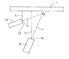
上記蒸着源Aに付設されたノズル12の先端開口13と、蒸着源Bの供給口14と、基材1との位置関係について、より詳しく説明すると、図3に示すように、上記蒸着源Bの供給口14は、Cu、InおよびGaの供給方向を示す仮想線I2と基材1とがなす角θ2が60°になるとともに、基材1表面からの最短距離L2が50mmとなる位置に配置されている。また、上記ノズル12の先端開口13は、Seの噴出方向を示す仮想線I1と基材とがなす角θ1が20°になるとともに、基材1表面からの最短距離L1が10mmとなる位置に配置されている。すなわち、これらの関係は、下記の一般式(1)~(4)を満たすようになっている。
L1/sinθ1≦L2/sinθ2・・・(1)
0°≦θ1≦30°・・・(2)
θ1≦θ2≦90°・・・(3)
L1<L2 ・・・(4)
θ1:蒸着源Aのノズルの先端開口からのVI族元素材料の噴出方向を示す仮想線I1と基材とがなす角(°)
θ2:蒸着源Bの供給口からのVI族以外の元素材料の供給方向を示す仮想線I2と基材とがなす角(°)
L1:蒸着源Aのノズルの先端開口と基材表面との最短距離(mm)
L2:蒸着源Bの供給口と基材表面との最短距離(mm)
L1/sinθ1≦L2/sinθ2・・・(1)
0°≦θ1≦30°・・・(2)
θ1≦θ2≦90°・・・(3)
L1<L2 ・・・(4)
θ1:蒸着源Aのノズルの先端開口からのVI族元素材料の噴出方向を示す仮想線I1と基材とがなす角(°)
θ2:蒸着源Bの供給口からのVI族以外の元素材料の供給方向を示す仮想線I2と基材とがなす角(°)
L1:蒸着源Aのノズルの先端開口と基材表面との最短距離(mm)
L2:蒸着源Bの供給口と基材表面との最短距離(mm)
そして、上記蒸着源Aに付設されたノズル12の開口径は、10mmであるが、ノズル12の開口径はこれに限らず、1~30mmの範囲にあることが好ましく、5~20mmの範囲にあることがより好ましい。すなわち、径が大きすぎると、噴出する材料の分布は良好となるが、Seの噴出圧が低くなり、SeがCu、InおよびGaの周りに充分回り込めなくなるおそれがあり、逆に、径が小さすぎると、Seの噴出圧は向上するが、良好な分布が得られずCIGS光吸収層3内でのSe材料の組成ムラが発生するおそれがあるためである。そして、上記ノズル12の周囲には、蒸着源Aから供給されるSe温度を調整できるよう加熱手段(例えば、電熱線)が配置されている(図示せず)が、他の方法によりSe温度の調整ができる場合にはこの加熱手段は設けなくてもよい。また、上記蒸着源Bには、Cu、InおよびGaの材料ごとに好適な加熱ができるように、蒸着源Bごとに独立した状態で加熱手段を設置することが好ましい。
なお、この例では、図3に示すように、ノズル12の先端開口13からSeの噴出方向(仮想線I1)と、蒸着源Bの供給口14からCu、In、Gaの供給方向(仮想線I2)とが、基材1の表面上(基材1表面からの距離が0mmの位置)で交わるように両者が配置されている。しかし、図4に示すように、両者の交点Pが、基材1の表面から下方に離れた位置となるように配置してもよく、とりわけ、交点Pが、基材1表面から下方に0~5mm離れた位置となる配置にすることが好ましい。上記交点Pが、基材1表面からの距離が離れすぎるような配置では、Cu、In、Gaに対するSeの回り込みが基板1近傍で起こらず、得られるCIGS光吸収層3におけるSeの組成比が悪くなる傾向にある。
この蒸着装置6を用いて、CIGS光吸収層3を得るには、まず、蒸着時の基材1の温度が550℃となるよう、蒸着室9に備えた加熱機構(図示せず)によって加熱する。なお、このとき、蒸着源AおよびBから発せられる熱によって、基材1の温度が高くなりすぎる場合があり、別途、基材1を冷却するための冷却機構(図示せず)を蒸着室9内に設けるようにしてもよい。そして、蒸着室9を真空状態にし、蒸着源A(Se材料ユニット)を350℃に加熱し、ノズル12を450℃に加熱し、その先端開口13から基材1に対して20°の角度でSeを噴射するとともに、蒸着源Bとして配置された、Cu、In、Gaの各材料ユニットを、それぞれ1300℃、1100℃、1100℃に加熱し、供給口14から基材1に向かって60°の角度でCu、In、Gaを供給することにより、基材1と蒸着源A,Bとが近接した状態であっても、Seを充分にCu、In、Gaの周りに回り込ますことができ、所望の組成比を有するカルコパイライト構造〔Cu(In1-X,GaX)Se2〕のCIGS光吸収層3を基材1上に得ることができる。
なお、上記蒸着源Aのノズル12は、その先端開口13からのSeの噴出方向を示す仮想線I1と基材1とがなす角θ1が20°となるように配置されているが、これに限らず、しかし、角θ1が0~30°の範囲の任意の角度となるように配置することが好ましい。また、上記蒸着源Bの供給口14は、Cu、InおよびGaの供給方向を示す仮想線I2と基材1とがなす角θ2が60°となるように配置されているが、これに限らず、しかし、上記角θ1より大きく、かつ、90°以下の範囲の任意の角度となるように配置することが好ましい。
また、上記ノズル12の先端開口13は、基材1表面からの最短距離L1が10mmに設定されているが、これに限らず、上記最短距離L1は、基材1表面から蒸着源Bの供給口14までの最短距離L2より短い距離の任意の範囲に設定することができる。そして、上記最短距離L2が50mmに設定されているが、これに限らず、5~70mmの範囲の任意の範囲に設定することができる。
なお、Seを供給するためのノズル12が付設された蒸着源Aと、Cu、InおよびGaを供給する供給口14を備えた蒸着源Bとが、蒸着室9内に各3個備えられているが、蒸着室9、基材1等のサイズや基材1の搬送速度等を考慮して、その数を増減することができる。また、蒸着源Aと蒸着源Bとが1:1の割合で設置されているが、必ずしもその必要はない。すなわち、図5で示すように、蒸着源Aに付設されたノズル12として、基材1方向へ延びる途中で分岐し、その先端開口13が複数形成されたものを用いると、蒸着源Bの個数に対して蒸着源Aの個数を少なくすることができる。この場合、蒸着源AからのSeの供給を一個所で制御できるため、管理が容易となる。さらに、蒸着源Aと蒸着源Bとを1:1で設置する場合であっても、図6に示すように、蒸着源Aに付設されたノズル12として、基材1方向へ延びる途中で2方向に分岐したものを用い、その分岐した各先端開口13からSeを噴射するようにしてもよい。この場合、蒸着源Bから供給されるその他の元素材料(Cu、In、Ga)の周りに、Seをより一層、回り込ますことができ、変換効率の高いCIGS光吸収層3をより効率よく形成することができる。
また、この蒸着装置6では、蒸着源Aとこれに付設されたノズル12の双方が、蒸着室9内に配設されているが、ノズル12を蒸着室9内に配設し、このノズル12を、蒸着室9外に配設された蒸着源Aと連結するようにしてもよい。蒸着源Aを蒸着室9の外に配設すると、蒸着源AからのSe供給の調整が容易となるため、Seのロスを少なくできるとともに、CIGS光吸収層の組成比をより容易に制御できる。そして、上記ノズル12と蒸着源Aとを着脱可能な弁手段によって連結すると、蒸着源Aの交換が容易となるため、好ましい。
そして、CIGS光吸収層3が形成された後、基材1をそのまま巻き取りロール10で巻き取っているが、CIGS光吸収層3の結晶性を高めるために、所定の温度でCIGS光吸収層3を加熱燃成した後、基材1を巻き取りロール10で巻き取るようにしてもよい。また、このCIGS光吸収層3の加熱燃成は、CIGS光吸収層3を形成した基材1を、一旦、巻き取りロール10で巻き取り、その後、巻き取った基材1を巻き出して行ってもよい。
さらに、上記CIGS光吸収層3の形成は、上記蒸着法だけでなく、その他にも、例えば、3段階法やバイレイヤー法等の蒸着法によっても行うことができる。
(バッファ層形成工程、表面電極層形成工程、電極形成工程)
つぎに、上記巻き取りロール10から、CIGS光吸収層3が形成された基材1を巻き出し、これを一定の長さごとに切断装置で切断し、所定サイズにする。そして、この所定サイズとなった基材1のCIGS光吸収層3上に、スパッタリング法によりバッファ層4を形成する。このバッファ層4は、スパッタリング法の他にも、化学浴堆積法(CBD法)等によっても形成することができる。そして、このバッファ層4上に、スパッタリング法により表面電極層5を形成し、基材1の裏面(CIGS光吸収層3等が形成された面の反対面)に、櫛型電極を形成することにより、CIGS太陽電池を得ることができる。
つぎに、上記巻き取りロール10から、CIGS光吸収層3が形成された基材1を巻き出し、これを一定の長さごとに切断装置で切断し、所定サイズにする。そして、この所定サイズとなった基材1のCIGS光吸収層3上に、スパッタリング法によりバッファ層4を形成する。このバッファ層4は、スパッタリング法の他にも、化学浴堆積法(CBD法)等によっても形成することができる。そして、このバッファ層4上に、スパッタリング法により表面電極層5を形成し、基材1の裏面(CIGS光吸収層3等が形成された面の反対面)に、櫛型電極を形成することにより、CIGS太陽電池を得ることができる。
上記CIGS太陽電池の製造方法によれば、基材1と蒸着源A,Bとが極めて近接しているため、高速かつ安定してCIGS光吸収層3を形成することができる。しかも、Seを、ノズル12を経由させることにより、Cu、In、Gaの供給口14より基材1に近い位置から噴射状態で供給するため、SeをCu、In、Gaと充分に反応させることができ、CIGS光吸収層3におけるSeの組成比を効率よく高めることができる。特に、蒸着源Aのノズル12の先端開口13と、蒸着源Bの供給口14と、基材1とが、上記の一般式(1)~(4)を満たす関係にあるため、とりわけ、SeをCu、In、Gaの周りに回り込ませることができ、互いに充分に反応させることができる。さらに、CIGS光吸収層3が、カルコパイライト構造を有するものであるため、薄膜でも高効率の光変換を行うことができるとともに、室温でも安定したものとすることができる。したがって、本発明の製法によれば、従来のように、Seを過剰に供給する必要がなく、変換効率の高いすぐれたCIGS太陽電池を、低コストで効率よく製造することができる。
なお、上記の実施の形態では、CIGS光吸収層形成工程までを、長尺状の基材1を用いたロールトゥロール方式で行い、バッファ層4以降の工程を、所定サイズに切断された基材1を用いた枚葉方式で行っているが、バッファ層4以降の工程を、CIGS光吸収層3形成工程と同様にロールトゥロール方式で行うようにしてもよい。この場合、表面電極層5の形成後、所定サイズに基材1を切断する。また、基材1を切断せずに用いてもよい。
また、上記の実施の形態では、長尺状の基材1の上に裏面電極層2を形成しているが、基材1に導電性があり、裏面電極層2の働きを兼ねることができる場合には、裏面電極層2を設けなくてもよい。
つぎに、実施例について比較例と併せて説明する。ただし、本発明は、以下の実施例に限定されるものではない。
〔実施例1〕
(裏面電極層の形成)
フェライト系SUS430からなる基材1(幅30nm、長さ100m、厚み50μm)の表面に、ロールトゥロール方式を用い、CrおよびMoをDCマグネトロンスパッタ法により、この順に積層して裏面電極層2(Cr:厚み100nm、Mo:厚み300nm)を形成した。
(裏面電極層の形成)
フェライト系SUS430からなる基材1(幅30nm、長さ100m、厚み50μm)の表面に、ロールトゥロール方式を用い、CrおよびMoをDCマグネトロンスパッタ法により、この順に積層して裏面電極層2(Cr:厚み100nm、Mo:厚み300nm)を形成した。
(CIGS光吸収層の形成)
つぎに、裏面電極層2が形成された基材1を、上記の実施の形態で用いた蒸着装置6(図2参照)の巻き出しロール7および巻き取りロール10に掛け渡し、裏面電極層2の上に、CIGS光吸収層3を形成した。すなわち、蒸着源Aのノズル12として、その先端開口13の開口径が10mmのノズルを用意するとともに、蒸着源Bとして、その供給口14の開口径が27.5mmのものを用意した。そして、蒸着装置6の蒸着室9において、蒸着源Aのノズル12の先端開口13と、蒸着源Bの供給口14と、基材1とが、下記に示す関係となるように配置した。
・蒸着源Aのノズル12の先端開口13からSeの噴出方向を示す仮想線I1と基材1とがなす角θ1が20°。
・蒸着源Bの供給口14からCu、In、Gaの供給方向を示す仮想線I2と基材1とがなす角θ2が90°。
・蒸着源Aのノズル12の先端開口13と基材1表面との最短距離L1が15mm。
・蒸着源Bの供給口14と基材1表面との最短距離L2が50mm。
・仮想線I1と仮想線I2との交点Pが、基材1表面から下方に2mm離れた位置。
つぎに、裏面電極層2が形成された基材1を、上記の実施の形態で用いた蒸着装置6(図2参照)の巻き出しロール7および巻き取りロール10に掛け渡し、裏面電極層2の上に、CIGS光吸収層3を形成した。すなわち、蒸着源Aのノズル12として、その先端開口13の開口径が10mmのノズルを用意するとともに、蒸着源Bとして、その供給口14の開口径が27.5mmのものを用意した。そして、蒸着装置6の蒸着室9において、蒸着源Aのノズル12の先端開口13と、蒸着源Bの供給口14と、基材1とが、下記に示す関係となるように配置した。
・蒸着源Aのノズル12の先端開口13からSeの噴出方向を示す仮想線I1と基材1とがなす角θ1が20°。
・蒸着源Bの供給口14からCu、In、Gaの供給方向を示す仮想線I2と基材1とがなす角θ2が90°。
・蒸着源Aのノズル12の先端開口13と基材1表面との最短距離L1が15mm。
・蒸着源Bの供給口14と基材1表面との最短距離L2が50mm。
・仮想線I1と仮想線I2との交点Pが、基材1表面から下方に2mm離れた位置。
そして、蒸着装置6内の圧力を1×10⁻³Paにし、蒸着室9内に配設されたハロゲンランプを備えた基材加熱機構(図示せず)により、基材1の表面温度が250℃になるよう加熱するとともに、蒸着源Bとして配置されたCu、In、Gaの各材料ユニットを、それぞれ1300℃、1100℃、1100℃となるように加熱した。また、蒸着源Aの材料ユニットを350℃となるように加熱するとともに、ノズル12を450℃となるように加熱した。
そして、巻き出しロール7から基材1を1m/minの速度で巻き出し、巻き取りロール10に向かって蒸着室9内を走行させ、この基材1に対して、Ga、In、Cuの順で並べられた各材料ユニット由来のGa、In、Cuを蒸着源Bの供給口14から供給するとともに、Seを蒸着源Aのノズル12先端開口13から噴射状態で供給し、カルコパイライト構造を有するCIGS光吸収層3を、基材1の裏面電極層2が形成された面に連続的に形成した。さらに、CIGS光吸収層3の結晶性を良好なものとするため、蒸着室9内に備えられた焼成機構(図示せず)により、上記CIGS光吸収層3を550℃の温度で15分間焼成し、その後、巻き取り室11の巻き取りロール10で巻き取った。
(CIGS太陽電池の製造)
上記巻き取りロール10から、裏面電極層2、CIGS光吸収層3がこの順で形成された基材1を巻き出し、これを100mmごとに切断装置で切断した。そして、この切断された基材1のCIGS光吸収層3が形成された面に、CBD法によりCdSからなるバッファ層4(厚み50μm)を形成した。さらに、上記バッファ層4の上に、スパッタリング法によりZnO層(厚み100nm)、ITO層(厚み300nm)をこの順で形成し、表面電極層5とした。そして、基材1の裏面(CIGS光吸収層3等が形成された面の反対面)に、NiCr/Alからなる櫛型電極を形成し、CIGS太陽電池を完成した。
上記巻き取りロール10から、裏面電極層2、CIGS光吸収層3がこの順で形成された基材1を巻き出し、これを100mmごとに切断装置で切断した。そして、この切断された基材1のCIGS光吸収層3が形成された面に、CBD法によりCdSからなるバッファ層4(厚み50μm)を形成した。さらに、上記バッファ層4の上に、スパッタリング法によりZnO層(厚み100nm)、ITO層(厚み300nm)をこの順で形成し、表面電極層5とした。そして、基材1の裏面(CIGS光吸収層3等が形成された面の反対面)に、NiCr/Alからなる櫛型電極を形成し、CIGS太陽電池を完成した。
〔実施例2〕
蒸着源Aのノズル12として、図6に示すように、2つに分岐するノズルを用い、Seをこの2つに分岐されたノズルによって2方向から噴射状態で供給するようにした他は、実施例1と同様にして、CIGS太陽電池を製造した。
蒸着源Aのノズル12として、図6に示すように、2つに分岐するノズルを用い、Seをこの2つに分岐されたノズルによって2方向から噴射状態で供給するようにした他は、実施例1と同様にして、CIGS太陽電池を製造した。
〔実施例3~12〕および〔比較例1〕、〔比較例3~8〕
蒸着源Aのノズル12の先端開口13と、蒸着源Bの供給口14と、基材1とが、後記の〔表1〕~〔表4〕に示す関係となるように配置を変更した他は、実施例1と同様にして、CIGS太陽電池を製造した。
蒸着源Aのノズル12の先端開口13と、蒸着源Bの供給口14と、基材1とが、後記の〔表1〕~〔表4〕に示す関係となるように配置を変更した他は、実施例1と同様にして、CIGS太陽電池を製造した。
〔比較例2〕
蒸着源AからのSeの供給を、ノズル12を用いずに行うとともに、その蒸着源Aの供給口と、基材1とが、表4に示す関係となるようにそれぞれの位置を変更し、蒸着源Aの供給口からSeの供給方向を示す仮想線と、仮想線I2との交点が、基材1表面から上方に10mm(下方に-10mm)離れた位置となるように変更した他は、実施例1と同様にして、CIGS太陽電池を製造した。
蒸着源AからのSeの供給を、ノズル12を用いずに行うとともに、その蒸着源Aの供給口と、基材1とが、表4に示す関係となるようにそれぞれの位置を変更し、蒸着源Aの供給口からSeの供給方向を示す仮想線と、仮想線I2との交点が、基材1表面から上方に10mm(下方に-10mm)離れた位置となるように変更した他は、実施例1と同様にして、CIGS太陽電池を製造した。
上記実施例および比較例のCIGS太陽電池をそれぞれ20個製造し、それらの変換効率を下記の手順に従って測定した。また、上記実施例および比較例におけるCIGS光吸収層3において、Seの回り込みの程度を評価するために、別途用意したフェライト系SUS430からなる基材(幅30nm、長さ100m、厚み50μm)の表面に、各実施例および比較例のCIGS光吸収層3の形成条件と同条件で、SeとInのみを蒸着し、SeとInとからなる蒸着層が積層された試験材を作製した。そして、この試験材の蒸着層におけるSe/Inの組成比を下記の手順に従って算出した。
測定および算出した結果を、後記の〔表1〕~〔表4〕に併せて示す。
測定および算出した結果を、後記の〔表1〕~〔表4〕に併せて示す。
〔変換効率〕
擬似太陽光(AM1.5)を100mm角以上の照射面積となるように、上記実施例および比較例のCIGS太陽電池のそれぞれ各20個に照射し、その変換効率をソーラシミュレータ(セルテスターYSS-150、山下電装社製)で測定した。そして、各実施例および比較例のCIGS太陽電池の平均変換効率を算出した。なお、上記測定は、放射照度1kW/m2、電池温度25℃の条件で行った。
擬似太陽光(AM1.5)を100mm角以上の照射面積となるように、上記実施例および比較例のCIGS太陽電池のそれぞれ各20個に照射し、その変換効率をソーラシミュレータ(セルテスターYSS-150、山下電装社製)で測定した。そして、各実施例および比較例のCIGS太陽電池の平均変換効率を算出した。なお、上記測定は、放射照度1kW/m2、電池温度25℃の条件で行った。
〔Se/Inの組成比〕
上記で作製した各試験材の蒸着層について、エネルギー分散型蛍光X線装置(EX-250、堀場製作所社製)を用いて、SeおよびIn元素の原子数濃度を測定し、それらの原子数濃度を元に、上記蒸着層のSe/Inの組成比を算出した。
上記で作製した各試験材の蒸着層について、エネルギー分散型蛍光X線装置(EX-250、堀場製作所社製)を用いて、SeおよびIn元素の原子数濃度を測定し、それらの原子数濃度を元に、上記蒸着層のSe/Inの組成比を算出した。

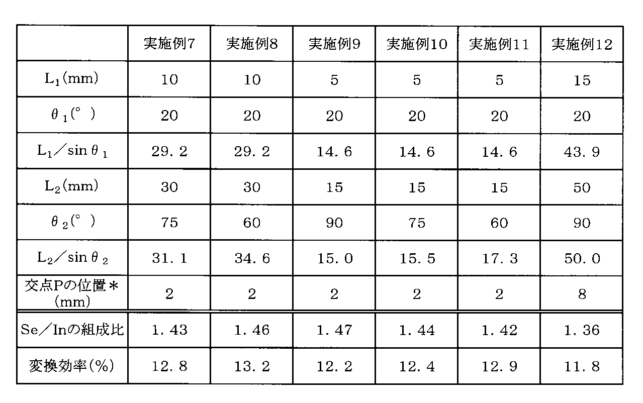
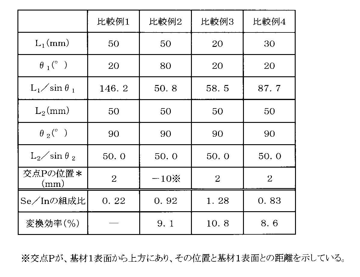
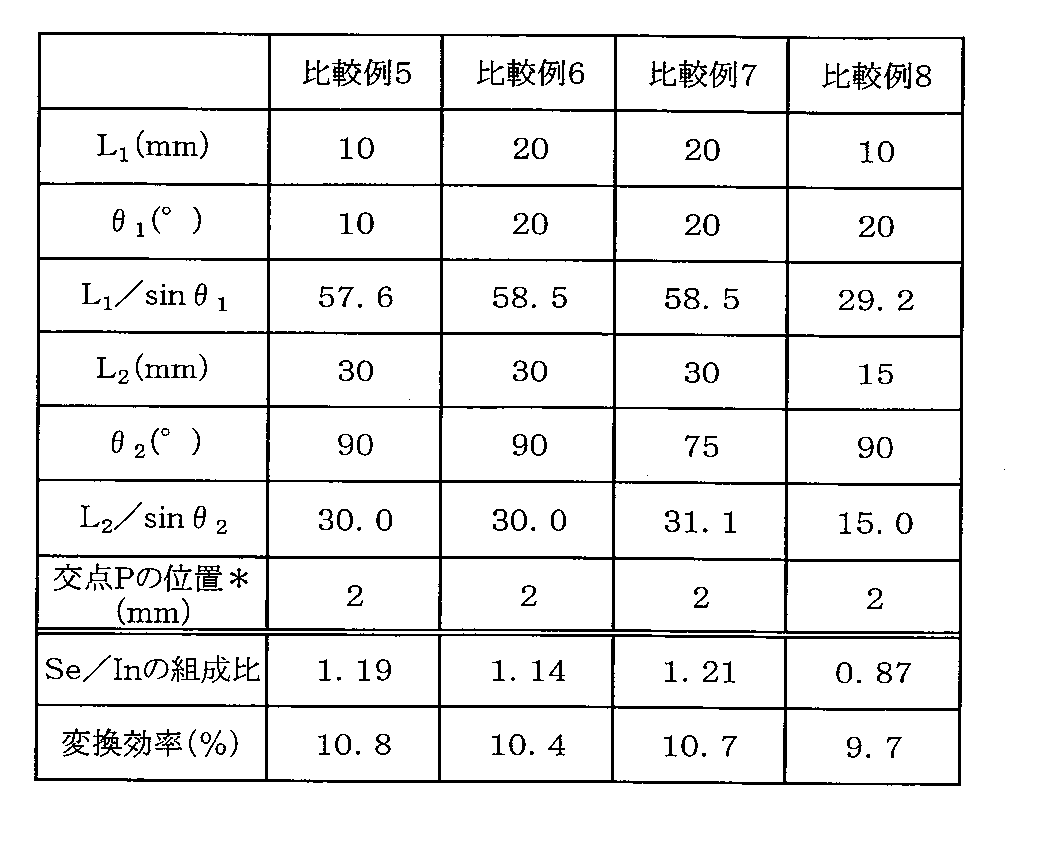
上記の結果より、実施例1~12は、試験材の蒸着層におけるSe/Inの組成比がいずれも1.36以上と高くなっており、本発明の蒸着法を用いることにより、基材と蒸着源との距離が近接していても、SeをInの周りに充分に回り込ますことができ、SeとInの反応が充分に行われたことが示された。これを裏付けるように、本発明の蒸着法によりCIGS光吸収層3を形成している実施例1~12のCIGS太陽電池は、その変換効率はいずれも11.8%以上と高効率になっていた。一方、蒸着源AからのSeの供給をノズルを用いて行っているものの、ノズルの先端開口と、蒸着源Bの供給口と、基材との位置関係が、本発明の範囲外となっている比較例1は、試験材の蒸着層におけるSe/Inの組成比が0.22と極めて低くなっており、CIGS太陽電池は発電しなかった。また、従来通りの蒸着法(蒸着源AからのSeの供給にノズルを用いない)によりCIGS光吸収層3を形成している比較例2では、試験材の蒸着層におけるSe/Inの組成比が0.92と低く、これに比例するように、CIGS太陽電池の変換効率も9.1%と低くなっていた。さらに、蒸着源Aのノズルの先端開口と蒸着源Bの供給口と基材とが上記の一般式(1)~(4)を満たす位置に配置されていない比較例3~8では、Se/Inの組成比が良好でなく、CIGS太陽電池の変換効率も低いものになっていた。
上記実施例においては、本発明における具体的な形態について示したが、上記実施例は単なる例示にすぎず、限定的に解釈されるものではない。当業者に明らかな様々な変形は、本発明の範囲内であることが企図されている。
本発明の化合物太陽電池の製造方法は、高変換効率を有する化合物太陽電池を高速で安定して製造するのに適している。
1 基材
12 ノズル
13 先端開口
14 供給口
A 蒸着源
B 蒸着源
12 ノズル
13 先端開口
14 供給口
A 蒸着源
B 蒸着源
Claims (4)
- 長尺状の基材を走行させながら、蒸着法により上記基材上に化合物半導体層を形成する化合物太陽電池の製造方法であって、上記化合物半導体層の形成を、VI族元素材料を供給するためのノズルが付設された蒸着源Aと、それ以外の元素材料を供給する供給口を備えた蒸着源Bを用いて行うようにし、上記蒸着源Bの供給口を基材から5~70mm離れた位置に配置するとともに、上記蒸着源Aのノズルの先端開口と蒸着源Bの供給口と基材とを下記の一般式(1)~(4)を満たす位置に配置し、上記VI族元素材料を、上記蒸着源Aのノズルの先端開口から加熱しながら噴射状態で供給するようにしたことを特徴とする化合物太陽電池の製造方法。
L1/sinθ1≦L2/sinθ2・・・(1)
0°≦θ1≦30°・・・(2)
θ1≦θ2≦90°・・・(3)
L1<L2 ・・・(4)
θ1:蒸着源Aのノズルの先端開口からのVI族元素材料の噴出方向を示す仮想線I1と基材とがなす角(°)
θ2:蒸着源Bの供給口からのVI族以外の元素材料の供給方向を示す仮想線I2と基材とがなす角(°)
L1:蒸着源Aのノズルの先端開口と基材表面との最短距離(mm)
L2:蒸着源Bの供給口と基材表面との最短距離(mm) - 上記化合物半導体層が、I族とIII族とVI族の元素からなるカルコパイライト構造を有するものである請求項1記載の化合物太陽電池の製造方法。
- 上記蒸着源Aに付設されたノズルが、複数に分岐するノズルに形成され、上記VI族元素材料が上記複数の分岐されたノズルによって多方向から噴射状態で供給されるようになっている請求項1または2記載の化合物太陽電池の製造方法。
- 上記化合物半導体層の形成が、真空槽内で行われており、上記VI族元素材料を噴射するためのノズルが上記真空槽内に配設されるとともに、上記ノズルに着脱可能な弁手段によって連結された蒸着源Aが上記真空槽外に配設され、上記蒸着源Aから真空槽内のノズルに上記VI族元素材料が供給されるようになっている請求項1~3のいずれか一項に記載の化合物太陽電池の製造方法。
Applications Claiming Priority (2)
| Application Number | Priority Date | Filing Date | Title |
|---|---|---|---|
| JP2012-153789 | 2012-07-09 | ||
| JP2012153789A JP2014015662A (ja) | 2012-07-09 | 2012-07-09 | 化合物太陽電池の製法 |
Publications (1)
| Publication Number | Publication Date |
|---|---|
| WO2014010371A1 true WO2014010371A1 (ja) | 2014-01-16 |
Family
ID=49915839
Family Applications (1)
| Application Number | Title | Priority Date | Filing Date |
|---|---|---|---|
| PCT/JP2013/066546 Ceased WO2014010371A1 (ja) | 2012-07-09 | 2013-06-17 | 化合物太陽電池の製法 |
Country Status (2)
| Country | Link |
|---|---|
| JP (1) | JP2014015662A (ja) |
| WO (1) | WO2014010371A1 (ja) |
Families Citing this family (2)
| Publication number | Priority date | Publication date | Assignee | Title |
|---|---|---|---|---|
| JP6432887B2 (ja) * | 2015-09-10 | 2018-12-05 | パナソニックIpマネジメント株式会社 | 積層体の製造方法および製造装置 |
| JP6983096B2 (ja) * | 2018-03-30 | 2021-12-17 | 株式会社アルバック | 真空蒸着装置用の蒸着源 |
Citations (4)
| Publication number | Priority date | Publication date | Assignee | Title |
|---|---|---|---|---|
| JP2005126757A (ja) * | 2003-10-23 | 2005-05-19 | Matsushita Electric Ind Co Ltd | 化合物薄膜の製造装置および方法 |
| JP2006508536A (ja) * | 2002-11-30 | 2006-03-09 | ハーン−マイトネル−インスチツート ベルリン ゲゼルシャフト ミット ベシュレンクテル ハフツング | 光学的なin−situプロセスコントロールを伴うカルコゲナイド半導体層の製造方法およびこの方法を実行する装置 |
| JP2006307278A (ja) * | 2005-04-28 | 2006-11-09 | Matsushita Electric Ind Co Ltd | 成膜装置および成膜方法 |
| JP2011077473A (ja) * | 2009-10-02 | 2011-04-14 | Meidensha Corp | 製膜方法及び製膜装置 |
-
2012
- 2012-07-09 JP JP2012153789A patent/JP2014015662A/ja not_active Withdrawn
-
2013
- 2013-06-17 WO PCT/JP2013/066546 patent/WO2014010371A1/ja not_active Ceased
Patent Citations (4)
| Publication number | Priority date | Publication date | Assignee | Title |
|---|---|---|---|---|
| JP2006508536A (ja) * | 2002-11-30 | 2006-03-09 | ハーン−マイトネル−インスチツート ベルリン ゲゼルシャフト ミット ベシュレンクテル ハフツング | 光学的なin−situプロセスコントロールを伴うカルコゲナイド半導体層の製造方法およびこの方法を実行する装置 |
| JP2005126757A (ja) * | 2003-10-23 | 2005-05-19 | Matsushita Electric Ind Co Ltd | 化合物薄膜の製造装置および方法 |
| JP2006307278A (ja) * | 2005-04-28 | 2006-11-09 | Matsushita Electric Ind Co Ltd | 成膜装置および成膜方法 |
| JP2011077473A (ja) * | 2009-10-02 | 2011-04-14 | Meidensha Corp | 製膜方法及び製膜装置 |
Also Published As
| Publication number | Publication date |
|---|---|
| JP2014015662A (ja) | 2014-01-30 |
Similar Documents
| Publication | Publication Date | Title |
|---|---|---|
| JP5246839B2 (ja) | 半導体薄膜の製造方法、半導体薄膜の製造装置、光電変換素子の製造方法及び光電変換素子 | |
| CN105794000A (zh) | 太阳能电池 | |
| US20150357486A1 (en) | Solar cell including multiple buffer layer formed by atomic layer deposition and method of fabricating the same | |
| JP6083785B2 (ja) | 化合物太陽電池およびその製造方法 | |
| JP2012007194A (ja) | 成膜装置および光電変換素子の製造方法 | |
| KR20130098143A (ko) | Cigs 태양 전지 제조를 위한 통합적 방법 | |
| US20160329446A1 (en) | Device for manufacturing integrated thin film solar cell | |
| US10211351B2 (en) | Photovoltaic cell with high efficiency CIGS absorber layer with low minority carrier lifetime and method of making thereof | |
| CN102694077B (zh) | 一种铜铟镓硒薄膜太阳能电池的制备方法 | |
| TW201344926A (zh) | 化合物太陽電池之製法 | |
| JP6265362B2 (ja) | Cigs系化合物太陽電池 | |
| WO2014010371A1 (ja) | 化合物太陽電池の製法 | |
| JP2017050337A (ja) | Cigs半導体前駆体膜の製造方法およびそれを用いたcigs半導体膜の製造方法並びにそれらを用いたcigs太陽電池の製造方法 | |
| CN104995749B (zh) | Cigs系化合物太阳能电池 | |
| WO2012090506A1 (ja) | 成膜装置および光電変換素子の製造方法 | |
| WO2012124430A1 (ja) | 太陽電池セルの製法および製造装置と太陽電池モジュールの製法 | |
| KR101734362B1 (ko) | Acigs 박막의 저온 형성방법과 이를 이용한 태양전지의 제조방법 | |
| JP2009114481A (ja) | 電析膜の形成方法、薄膜太陽電池及びその製造方法 | |
| WO2013035732A1 (ja) | Cigs膜の製法およびそれを用いるcigs太陽電池の製法 | |
| JP2014232797A (ja) | 半導体前駆構造物およびそれを用いて得られるcigs半導体構造物ならびにそれを用いるcigs太陽電池とその製造方法 | |
| JP2011176148A (ja) | 太陽電池モジュールの製造方法およびそれを用いて得られた太陽電池モジュール | |
| WO2016132637A1 (ja) | Cigs太陽電池およびその製造方法 | |
| JP2015164163A (ja) | 光電変換素子および太陽電池 | |
| JP5710368B2 (ja) | 光電変換素子および太陽電池 | |
| JP6861480B2 (ja) | 光電変換モジュールの製造方法 |
Legal Events
| Date | Code | Title | Description |
|---|---|---|---|
| 121 | Ep: the epo has been informed by wipo that ep was designated in this application |
Ref document number: 13816959 Country of ref document: EP Kind code of ref document: A1 |
|
| NENP | Non-entry into the national phase |
Ref country code: DE |
|
| 122 | Ep: pct application non-entry in european phase |
Ref document number: 13816959 Country of ref document: EP Kind code of ref document: A1 |