WO2014002361A1 - 固体撮像装置及びその製造方法 - Google Patents
固体撮像装置及びその製造方法 Download PDFInfo
- Publication number
- WO2014002361A1 WO2014002361A1 PCT/JP2013/002958 JP2013002958W WO2014002361A1 WO 2014002361 A1 WO2014002361 A1 WO 2014002361A1 JP 2013002958 W JP2013002958 W JP 2013002958W WO 2014002361 A1 WO2014002361 A1 WO 2014002361A1
- Authority
- WO
- WIPO (PCT)
- Prior art keywords
- region
- gate electrode
- forming
- transistor
- conductivity type
- Prior art date
Links
- 238000004519 manufacturing process Methods 0.000 title claims description 24
- 239000012535 impurity Substances 0.000 claims abstract description 133
- 239000004065 semiconductor Substances 0.000 claims abstract description 96
- 238000006243 chemical reaction Methods 0.000 claims abstract description 54
- 238000000926 separation method Methods 0.000 claims abstract description 11
- 238000002955 isolation Methods 0.000 claims description 82
- 230000003321 amplification Effects 0.000 claims description 80
- 238000003199 nucleic acid amplification method Methods 0.000 claims description 80
- 238000003384 imaging method Methods 0.000 claims description 72
- 238000000034 method Methods 0.000 claims description 26
- 238000001459 lithography Methods 0.000 claims description 18
- 238000003860 storage Methods 0.000 claims description 17
- 238000009825 accumulation Methods 0.000 abstract description 5
- 230000002093 peripheral effect Effects 0.000 abstract description 3
- 239000000758 substrate Substances 0.000 description 46
- 150000002500 ions Chemical class 0.000 description 26
- 239000010410 layer Substances 0.000 description 25
- 238000009792 diffusion process Methods 0.000 description 18
- 238000002513 implantation Methods 0.000 description 18
- 238000005468 ion implantation Methods 0.000 description 15
- 230000002829 reductive effect Effects 0.000 description 14
- 230000000875 corresponding effect Effects 0.000 description 13
- 230000035945 sensitivity Effects 0.000 description 13
- 230000007423 decrease Effects 0.000 description 10
- 230000015572 biosynthetic process Effects 0.000 description 9
- 239000011229 interlayer Substances 0.000 description 8
- 238000012545 processing Methods 0.000 description 8
- XUIMIQQOPSSXEZ-UHFFFAOYSA-N Silicon Chemical compound [Si] XUIMIQQOPSSXEZ-UHFFFAOYSA-N 0.000 description 6
- 238000005229 chemical vapour deposition Methods 0.000 description 6
- 230000006866 deterioration Effects 0.000 description 6
- 230000004048 modification Effects 0.000 description 6
- 238000012986 modification Methods 0.000 description 6
- 229910021420 polycrystalline silicon Inorganic materials 0.000 description 6
- 229920005591 polysilicon Polymers 0.000 description 6
- 229910052710 silicon Inorganic materials 0.000 description 6
- 239000010703 silicon Substances 0.000 description 6
- VYPSYNLAJGMNEJ-UHFFFAOYSA-N Silicium dioxide Chemical compound O=[Si]=O VYPSYNLAJGMNEJ-UHFFFAOYSA-N 0.000 description 5
- 230000009467 reduction Effects 0.000 description 5
- 229910052814 silicon oxide Inorganic materials 0.000 description 5
- 238000001312 dry etching Methods 0.000 description 4
- 230000003647 oxidation Effects 0.000 description 4
- 238000007254 oxidation reaction Methods 0.000 description 4
- 230000002441 reversible effect Effects 0.000 description 4
- 230000000694 effects Effects 0.000 description 3
- 230000000873 masking effect Effects 0.000 description 3
- 230000003071 parasitic effect Effects 0.000 description 3
- 230000015556 catabolic process Effects 0.000 description 2
- 230000008859 change Effects 0.000 description 2
- 230000001276 controlling effect Effects 0.000 description 2
- 230000007547 defect Effects 0.000 description 2
- 238000006731 degradation reaction Methods 0.000 description 2
- 238000013461 design Methods 0.000 description 2
- 238000010586 diagram Methods 0.000 description 2
- 230000001629 suppression Effects 0.000 description 2
- 241000519995 Stachys sylvatica Species 0.000 description 1
- 230000003213 activating effect Effects 0.000 description 1
- 230000004913 activation Effects 0.000 description 1
- 229910021417 amorphous silicon Inorganic materials 0.000 description 1
- 238000000137 annealing Methods 0.000 description 1
- 230000002596 correlated effect Effects 0.000 description 1
- 238000000151 deposition Methods 0.000 description 1
- 238000005530 etching Methods 0.000 description 1
- 239000000284 extract Substances 0.000 description 1
- 230000005669 field effect Effects 0.000 description 1
- 239000007943 implant Substances 0.000 description 1
- 238000011065 in-situ storage Methods 0.000 description 1
- 230000002401 inhibitory effect Effects 0.000 description 1
- 238000009413 insulation Methods 0.000 description 1
- 238000011835 investigation Methods 0.000 description 1
- 238000010030 laminating Methods 0.000 description 1
- 239000011159 matrix material Substances 0.000 description 1
- 239000011368 organic material Substances 0.000 description 1
- 238000005498 polishing Methods 0.000 description 1
- 230000008569 process Effects 0.000 description 1
- 230000001681 protective effect Effects 0.000 description 1
- 230000007261 regionalization Effects 0.000 description 1
- 238000005070 sampling Methods 0.000 description 1
- 239000000126 substance Substances 0.000 description 1
Images


Classifications
-
- H—ELECTRICITY
- H01—ELECTRIC ELEMENTS
- H01L—SEMICONDUCTOR DEVICES NOT COVERED BY CLASS H10
- H01L27/00—Devices consisting of a plurality of semiconductor or other solid-state components formed in or on a common substrate
- H01L27/14—Devices consisting of a plurality of semiconductor or other solid-state components formed in or on a common substrate including semiconductor components sensitive to infrared radiation, light, electromagnetic radiation of shorter wavelength or corpuscular radiation and specially adapted either for the conversion of the energy of such radiation into electrical energy or for the control of electrical energy by such radiation
- H01L27/144—Devices controlled by radiation
- H01L27/146—Imager structures
- H01L27/14643—Photodiode arrays; MOS imagers
-
- H—ELECTRICITY
- H01—ELECTRIC ELEMENTS
- H01L—SEMICONDUCTOR DEVICES NOT COVERED BY CLASS H10
- H01L21/00—Processes or apparatus adapted for the manufacture or treatment of semiconductor or solid state devices or of parts thereof
- H01L21/02—Manufacture or treatment of semiconductor devices or of parts thereof
- H01L21/04—Manufacture or treatment of semiconductor devices or of parts thereof the devices having at least one potential-jump barrier or surface barrier, e.g. PN junction, depletion layer or carrier concentration layer
- H01L21/18—Manufacture or treatment of semiconductor devices or of parts thereof the devices having at least one potential-jump barrier or surface barrier, e.g. PN junction, depletion layer or carrier concentration layer the devices having semiconductor bodies comprising elements of Group IV of the Periodic System or AIIIBV compounds with or without impurities, e.g. doping materials
- H01L21/26—Bombardment with radiation
- H01L21/263—Bombardment with radiation with high-energy radiation
- H01L21/265—Bombardment with radiation with high-energy radiation producing ion implantation
- H01L21/266—Bombardment with radiation with high-energy radiation producing ion implantation using masks
-
- H—ELECTRICITY
- H01—ELECTRIC ELEMENTS
- H01L—SEMICONDUCTOR DEVICES NOT COVERED BY CLASS H10
- H01L21/00—Processes or apparatus adapted for the manufacture or treatment of semiconductor or solid state devices or of parts thereof
- H01L21/70—Manufacture or treatment of devices consisting of a plurality of solid state components formed in or on a common substrate or of parts thereof; Manufacture of integrated circuit devices or of parts thereof
- H01L21/77—Manufacture or treatment of devices consisting of a plurality of solid state components or integrated circuits formed in, or on, a common substrate
- H01L21/78—Manufacture or treatment of devices consisting of a plurality of solid state components or integrated circuits formed in, or on, a common substrate with subsequent division of the substrate into plural individual devices
- H01L21/82—Manufacture or treatment of devices consisting of a plurality of solid state components or integrated circuits formed in, or on, a common substrate with subsequent division of the substrate into plural individual devices to produce devices, e.g. integrated circuits, each consisting of a plurality of components
- H01L21/822—Manufacture or treatment of devices consisting of a plurality of solid state components or integrated circuits formed in, or on, a common substrate with subsequent division of the substrate into plural individual devices to produce devices, e.g. integrated circuits, each consisting of a plurality of components the substrate being a semiconductor, using silicon technology
- H01L21/8232—Field-effect technology
- H01L21/8234—MIS technology, i.e. integration processes of field effect transistors of the conductor-insulator-semiconductor type
- H01L21/823437—MIS technology, i.e. integration processes of field effect transistors of the conductor-insulator-semiconductor type with a particular manufacturing method of the gate conductors, e.g. particular materials, shapes
- H01L21/823456—MIS technology, i.e. integration processes of field effect transistors of the conductor-insulator-semiconductor type with a particular manufacturing method of the gate conductors, e.g. particular materials, shapes gate conductors with different shapes, lengths or dimensions
-
- H—ELECTRICITY
- H01—ELECTRIC ELEMENTS
- H01L—SEMICONDUCTOR DEVICES NOT COVERED BY CLASS H10
- H01L21/00—Processes or apparatus adapted for the manufacture or treatment of semiconductor or solid state devices or of parts thereof
- H01L21/70—Manufacture or treatment of devices consisting of a plurality of solid state components formed in or on a common substrate or of parts thereof; Manufacture of integrated circuit devices or of parts thereof
- H01L21/77—Manufacture or treatment of devices consisting of a plurality of solid state components or integrated circuits formed in, or on, a common substrate
- H01L21/78—Manufacture or treatment of devices consisting of a plurality of solid state components or integrated circuits formed in, or on, a common substrate with subsequent division of the substrate into plural individual devices
- H01L21/82—Manufacture or treatment of devices consisting of a plurality of solid state components or integrated circuits formed in, or on, a common substrate with subsequent division of the substrate into plural individual devices to produce devices, e.g. integrated circuits, each consisting of a plurality of components
- H01L21/822—Manufacture or treatment of devices consisting of a plurality of solid state components or integrated circuits formed in, or on, a common substrate with subsequent division of the substrate into plural individual devices to produce devices, e.g. integrated circuits, each consisting of a plurality of components the substrate being a semiconductor, using silicon technology
- H01L21/8232—Field-effect technology
- H01L21/8234—MIS technology, i.e. integration processes of field effect transistors of the conductor-insulator-semiconductor type
- H01L21/823481—MIS technology, i.e. integration processes of field effect transistors of the conductor-insulator-semiconductor type isolation region manufacturing related aspects, e.g. to avoid interaction of isolation region with adjacent structure
-
- H—ELECTRICITY
- H01—ELECTRIC ELEMENTS
- H01L—SEMICONDUCTOR DEVICES NOT COVERED BY CLASS H10
- H01L27/00—Devices consisting of a plurality of semiconductor or other solid-state components formed in or on a common substrate
- H01L27/14—Devices consisting of a plurality of semiconductor or other solid-state components formed in or on a common substrate including semiconductor components sensitive to infrared radiation, light, electromagnetic radiation of shorter wavelength or corpuscular radiation and specially adapted either for the conversion of the energy of such radiation into electrical energy or for the control of electrical energy by such radiation
- H01L27/144—Devices controlled by radiation
- H01L27/146—Imager structures
- H01L27/14601—Structural or functional details thereof
- H01L27/14609—Pixel-elements with integrated switching, control, storage or amplification elements
- H01L27/1461—Pixel-elements with integrated switching, control, storage or amplification elements characterised by the photosensitive area
-
- H—ELECTRICITY
- H01—ELECTRIC ELEMENTS
- H01L—SEMICONDUCTOR DEVICES NOT COVERED BY CLASS H10
- H01L27/00—Devices consisting of a plurality of semiconductor or other solid-state components formed in or on a common substrate
- H01L27/14—Devices consisting of a plurality of semiconductor or other solid-state components formed in or on a common substrate including semiconductor components sensitive to infrared radiation, light, electromagnetic radiation of shorter wavelength or corpuscular radiation and specially adapted either for the conversion of the energy of such radiation into electrical energy or for the control of electrical energy by such radiation
- H01L27/144—Devices controlled by radiation
- H01L27/146—Imager structures
- H01L27/14601—Structural or functional details thereof
- H01L27/14609—Pixel-elements with integrated switching, control, storage or amplification elements
- H01L27/14612—Pixel-elements with integrated switching, control, storage or amplification elements involving a transistor
-
- H—ELECTRICITY
- H01—ELECTRIC ELEMENTS
- H01L—SEMICONDUCTOR DEVICES NOT COVERED BY CLASS H10
- H01L27/00—Devices consisting of a plurality of semiconductor or other solid-state components formed in or on a common substrate
- H01L27/14—Devices consisting of a plurality of semiconductor or other solid-state components formed in or on a common substrate including semiconductor components sensitive to infrared radiation, light, electromagnetic radiation of shorter wavelength or corpuscular radiation and specially adapted either for the conversion of the energy of such radiation into electrical energy or for the control of electrical energy by such radiation
- H01L27/144—Devices controlled by radiation
- H01L27/146—Imager structures
- H01L27/14601—Structural or functional details thereof
- H01L27/1463—Pixel isolation structures
-
- H—ELECTRICITY
- H01—ELECTRIC ELEMENTS
- H01L—SEMICONDUCTOR DEVICES NOT COVERED BY CLASS H10
- H01L27/00—Devices consisting of a plurality of semiconductor or other solid-state components formed in or on a common substrate
- H01L27/14—Devices consisting of a plurality of semiconductor or other solid-state components formed in or on a common substrate including semiconductor components sensitive to infrared radiation, light, electromagnetic radiation of shorter wavelength or corpuscular radiation and specially adapted either for the conversion of the energy of such radiation into electrical energy or for the control of electrical energy by such radiation
- H01L27/144—Devices controlled by radiation
- H01L27/146—Imager structures
- H01L27/14665—Imagers using a photoconductor layer
-
- H—ELECTRICITY
- H01—ELECTRIC ELEMENTS
- H01L—SEMICONDUCTOR DEVICES NOT COVERED BY CLASS H10
- H01L27/00—Devices consisting of a plurality of semiconductor or other solid-state components formed in or on a common substrate
- H01L27/14—Devices consisting of a plurality of semiconductor or other solid-state components formed in or on a common substrate including semiconductor components sensitive to infrared radiation, light, electromagnetic radiation of shorter wavelength or corpuscular radiation and specially adapted either for the conversion of the energy of such radiation into electrical energy or for the control of electrical energy by such radiation
- H01L27/144—Devices controlled by radiation
- H01L27/146—Imager structures
- H01L27/14683—Processes or apparatus peculiar to the manufacture or treatment of these devices or parts thereof
- H01L27/14689—MOS based technologies
-
- H—ELECTRICITY
- H04—ELECTRIC COMMUNICATION TECHNIQUE
- H04N—PICTORIAL COMMUNICATION, e.g. TELEVISION
- H04N25/00—Circuitry of solid-state image sensors [SSIS]; Control thereof
- H04N25/60—Noise processing, e.g. detecting, correcting, reducing or removing noise
- H04N25/65—Noise processing, e.g. detecting, correcting, reducing or removing noise applied to reset noise, e.g. KTC noise related to CMOS structures by techniques other than CDS
-
- H—ELECTRICITY
- H04—ELECTRIC COMMUNICATION TECHNIQUE
- H04N—PICTORIAL COMMUNICATION, e.g. TELEVISION
- H04N25/00—Circuitry of solid-state image sensors [SSIS]; Control thereof
- H04N25/70—SSIS architectures; Circuits associated therewith
- H04N25/71—Charge-coupled device [CCD] sensors; Charge-transfer registers specially adapted for CCD sensors
- H04N25/75—Circuitry for providing, modifying or processing image signals from the pixel array
-
- H—ELECTRICITY
- H04—ELECTRIC COMMUNICATION TECHNIQUE
- H04N—PICTORIAL COMMUNICATION, e.g. TELEVISION
- H04N25/00—Circuitry of solid-state image sensors [SSIS]; Control thereof
- H04N25/70—SSIS architectures; Circuits associated therewith
- H04N25/76—Addressed sensors, e.g. MOS or CMOS sensors
- H04N25/78—Readout circuits for addressed sensors, e.g. output amplifiers or A/D converters
Definitions
- the present invention relates to a solid-state imaging device and a manufacturing method thereof.
- MOS Metal-Oxide-Semiconductor
- solid-state imaging devices are mounted on mobile device cameras, in-vehicle cameras, surveillance cameras, and the like. These solid-state imaging devices are required to have a high-resolution imaging capability, and the solid-state imaging devices need to be miniaturized and have a large number of pixels.
- the size of the photodiode is also reduced due to pixel miniaturization.
- the sensitivity of the pixel decreases due to a decrease in the saturation signal amount and a decrease in the aperture ratio.
- a so-called insulation isolation method using a LOCOS (Local Oxidation of Silicon) isolation method or an STI (Shallow Trench Isolation) isolation method is used as a method for forming element isolation in the solid-state imaging device.
- STI forms a trench in the upper part of a semiconductor substrate, and embeds a silicon oxide film in the formed trench to constitute element isolation. Defects and interface states or stress caused by etching damage during the formation of trenches cause leakage current. The charge due to the leakage current is indistinguishable from the signal charge photoelectrically converted by the photodiode, and thus becomes noise and degrades the performance of the image sensor.
- Patent Document 1 As one method for suppressing leakage current, a method of forming an element isolation region with an impurity semiconductor layer is known (see, for example, Patent Document 1).
- the element isolation region in contact with the n-type semiconductor region serving as the floating diffusion (FD) portion is formed by STI, and the element isolation region other than the region in contact with the FD portion is p.
- a diffusion element isolation region of the mold is formed.
- the element isolation region in contact with the n-type semiconductor region serving as the FD portion is formed by STI, the capacitance formed between the n-type semiconductor region of the FD portion and the semiconductor substrate is reduced.
- the element isolation region other than the region in contact with the FD portion is formed of a p-type diffusion element isolation region, leakage current can be suppressed.
- a stacked solid-state imaging device is formed by stacking a photoelectric conversion film above a semiconductor substrate, that is, on the outermost surface. Light is incident from above the laminated film, and charges generated by photoelectric conversion in the photoelectric conversion film are accumulated in a charge accumulation region (FD), and on a semiconductor substrate by a CCD (Charge-Coupled Device) circuit or a CMOS (Complementary-MOS) circuit. Read (for example, refer to Patent Document 2).
- CCD Charge-Coupled Device
- CMOS Complementary-MOS
- a pn junction serving as an FD that accumulates signal charges is formed on a semiconductor substrate.
- a contact for transmitting a signal charge photoelectrically converted by the photoelectric conversion film is electrically connected to the pn junction.
- the leakage current at the pn junction of the semiconductor substrate is large.
- the signal charge accumulation time in the FD is longer than that in the conventional MOS sensor, the sensitivity decrease due to the leakage current becomes more remarkable in the stacked solid-state imaging device.
- the solid-state imaging device described in Patent Document 1 has a problem of an increase in gate capacity.
- the increase in the gate capacitance causes a decrease in gain in the amplification transistor and causes a decrease in sensitivity.
- increase in the gate capacitance becomes a parasitic capacitance of the FD portion electrically connected to a gate electrode, since the total capacity C FD of the FD portion is increased, when converting the charges obtained by the photoelectric conversion to the signal voltage There is also a problem that the conversion efficiency is reduced.
- an STI is formed instead of a diffusion element isolation region in a region in contact with the FD portion.
- element isolation having the STI structure is insufficient as a countermeasure against the problem of leakage current.
- this is a serious problem in a stacked solid-state imaging device in which leakage current in the FD portion is a problem.
- the inventors of the present application have found that if diffusion element isolation is used in the element isolation region, the alignment budget becomes large and it is difficult to reduce the pixel size.
- an object of the present invention is to improve sensitivity by suppressing an increase in gate capacitance while suppressing deterioration in signal-to-noise ratio due to occurrence of leakage current.
- Another object of the present invention is to suppress variations in transistor characteristics and performance degradation due to a decrease in effective channel width by inhibiting diffusion of impurity ions from the diffusion element isolation into the channel region.
- Another object of the present invention is to reduce the alignment budget so that the pixels can be more easily miniaturized.
- the present invention does not have to solve all of the above objects, and only needs to achieve at least one object.
- the solid-state imaging device has a configuration in which the distance in the gate width direction in the diffusion element separation is larger in the channel region than in the source / drain region.
- a solid-state imaging device includes a first conductivity type semiconductor region and a plurality of unit pixel cells arranged in the semiconductor region.
- the unit pixel cell includes a photoelectric conversion unit and a photoelectric conversion unit.
- a second conductivity type impurity region for forming a storage diode for storing the signal charge generated in step with the semiconductor region, an amplification transistor formed in the semiconductor region and having a gate electrode electrically connected to the impurity region;
- a first isolation region formed in a region around the amplification transistor in the semiconductor region and introduced with an impurity of the first conductivity type.
- the amplification transistor includes a gate electrode and a first isolation region in the semiconductor region.
- a first conductivity type source region or a second conductivity type drain region formed between the channel region and a channel region formed below the gate electrode in the semiconductor region;
- the width direction of the spacing of the gate electrode in the range, a portion sandwiching the channel region is greater than the portion sandwiching the source or drain region.
- the interval in the width direction of the gate electrode in the first isolation region into which the impurity is introduced is larger in the portion sandwiching the channel region than in the portion sandwiching the source region or drain region. Therefore, since the amount of protrusion of the gate electrode to the channel region (gate protrusion amount) in the amplification transistor is reduced, the increase in the gate capacitance is suppressed while suppressing the deterioration of the signal-to-noise ratio value due to the occurrence of the leakage current. be able to. As a result, the sensitivity of the solid-state imaging device can be improved. In addition, since the gate protrusion amount is reduced, a reduction in effective channel width due to diffusion of impurity ions from the first isolation region is suppressed, so that variations in transistor characteristics and performance deterioration can be reduced.
- the first separation region may also be formed in a region around the impurity region.
- the impurity region which is the FD portion is insulated by the first isolation region made of the impurity semiconductor layer, the gate capacitance which is a parasitic capacitance of the FD portion is reduced. As a result, it is possible to achieve both the reduction of the total capacity C FD of the leakage suppression and FD portion. In particular, in a stacked solid-state imaging device in which leakage current in the FD portion is a big problem, a more remarkable effect is shown.
- the photoelectric conversion unit is formed above the semiconductor region, photoelectric conversion film that photoelectrically converts incident light, a transparent electrode formed above the photoelectric conversion film, the semiconductor region, and photoelectric conversion
- a pixel electrode formed between the pixel electrode and the impurity region; and the pixel electrode and the impurity region may be electrically connected to each other.
- the present invention can obtain more remarkable effects.
- the end surface in the width direction of the gate electrode and the end surface below the gate electrode in the first separation region may be the same surface.
- the amount of gate protrusion can be minimized.
- the reduction of the effective channel width can be suppressed, the sensitivity of the solid-state imaging device can be improved, and variations in transistor characteristics and performance deterioration can be further reduced.
- the impurity concentration of the first isolation region is set to be higher than the impurity concentration of the semiconductor region, and an impurity of the first conductivity type is introduced into the semiconductor region, so that adjacent unit pixel cells You may further provide the 2nd isolation
- the impurity concentration of the first isolation region and the impurity concentration of the second isolation region may be the same.
- the unit pixel cell has a reset transistor that resets the potential of the gate electrode of the amplification transistor, the channel region of the amplification transistor is made of the first conductivity type impurity, and the reset transistor The channel region may be made of a first conductivity type impurity.
- Vth threshold voltage
- the unit pixel cell has a reset transistor that resets the potential of the gate electrode of the amplification transistor, and the channel region of the amplification transistor is made of the second conductivity type impurity,
- the channel region may be made of a first conductivity type impurity.
- the threshold voltage of the reset transistor can be set high to reduce off-leakage, so that FD leakage can be reduced.
- the threshold voltage of the amplification transistor can be set low, it can be reliably driven in the saturation region.
- the method for manufacturing a solid-state imaging device includes a step of selectively forming a gate electrode on a semiconductor region of the first conductivity type, and a width of a region including the gate electrode on the semiconductor region by a lithography method. Forming a pattern smaller than the width of the gate electrode, using the gate electrode and the pattern as a mask, implanting a first conductivity type impurity into the semiconductor region, and removing the pattern Thereafter, a step of forming a source / drain region by selectively injecting a second conductivity type impurity into a region where the pattern in the semiconductor region has been formed is provided.
- an isolation region for element isolation is formed, so that the alignment budget can be reduced. As a result, pixel miniaturization can be realized more easily.
- the channel region of the amplification transistor and the amplification transistor are selectively implanted by selectively injecting the first conductivity type impurity into the semiconductor region before the step of forming the gate electrode.
- the channel region of the reset transistor may be formed larger than the gate width of the reset transistor.
- the channel regions of the amplification transistor and the reset transistor are formed before forming the gate electrode, there is a region where the threshold voltage is partially lowered directly under each gate electrode due to the influence of misalignment or the like. It can be prevented from being formed. As a result, a channel region having a uniform impurity concentration, that is, a threshold voltage can be reliably formed.
- the method for manufacturing a solid-state imaging device includes a step of forming a channel region of an amplification transistor by selectively injecting a second conductivity type impurity into a semiconductor region before the step of forming a gate electrode.
- the channel region of the amplification transistor may be formed smaller than the gate width of the amplification transistor, while the channel region of the reset transistor may be formed larger than the gate width of the reset transistor.
- the channel region can be reliably formed inside the gate width of the amplification transistor. As a result, it is possible to prevent a leak path between the source and drain regions from being formed outside the gate electrode.
- the method for manufacturing a solid-state imaging device includes a step of forming a channel region of an amplification transistor by selectively injecting a second conductivity type impurity into a semiconductor region before the step of forming a gate electrode.
- the channel region of the amplification transistor is formed larger than the gate width of the amplification transistor, and the channel region of the reset transistor is formed larger than the gate width of the reset transistor to form the isolation region.
- the impurity concentration of one conductivity type depends on the process for forming the channel region of the amplification transistor. It may be higher than the impurity concentration of the second conductivity type in.
- the conductivity type can be reversed by impurity implantation at the time of forming the isolation region. Therefore, it is possible to prevent a leak path between the source and drain regions from being formed outside the gate electrode. Further, since the resist pattern for forming the channel region can be expanded to the outside of the gate electrode, the margin during lithography can be expanded.
- the increase in gate capacitance can be suppressed while suppressing the deterioration of the signal-to-noise ratio due to the occurrence of leakage current, so that the sensitivity can be improved.
- variations in transistor characteristics and performance degradation can be suppressed, and pixel miniaturization can be performed more easily.
- FIG. 1 is a circuit diagram showing a solid-state imaging device according to the first embodiment.
- FIG. 2 is a schematic cross-sectional view showing one unit pixel cell in the solid-state imaging device according to the first embodiment.
- FIG. 3 is a schematic diagram showing a potential of a portion along the line III-III in FIG. 2 in the unit pixel cell according to the first embodiment.
- FIG. 4 is a schematic plan view showing the configuration of the unit pixel cell according to the first embodiment.
- 5A and 5B schematically show an active region and an element isolation region in the unit pixel cell according to the first embodiment, and FIG. 5A shows a cross section taken along the line Va-Va in FIG.
- FIG. 5B is a cross-sectional view taken along line Vb-Vb in FIG.
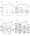
- FIG. 6A to FIG. 6D are plan views in order of steps showing the method for manufacturing the solid-state imaging device according to the first embodiment.
- FIG. 7A to FIG. 7D are plan views in the order of steps showing the method for manufacturing the solid-state imaging device according to the second embodiment.
- FIG. 8A to FIG. 8D are plan views in order of steps showing a method for manufacturing a solid-state imaging device according to a modification of the second embodiment.
- FIG. 1 shows a circuit configuration of the solid-state imaging device according to the first embodiment.
- the solid-state imaging device is a stacked solid-state imaging device, and is a photosensitive region composed of a plurality of unit pixel cells 13 arranged in a matrix on a semiconductor substrate. (Pixel region) and a drive circuit unit that sequentially drives the plurality of unit pixel cells 13 and extracts a photoelectrically converted signal.
- the drive circuit unit includes a vertical scanning unit (row scanning circuit) 15, a photoelectric conversion unit control line 16, a horizontal signal reading unit (column scanning circuit) 20, and a column signal processing unit (row signal) connected to the horizontal signal reading unit 20.
- Storage unit) 19 a vertical signal line (vertical signal line wiring) 17 connecting the column signal processing unit 19 and the unit pixel cell 13, a load unit 18 connected to the vertical signal line 17, and each unit pixel cell 13.
- An amplifier (feedback amplifier) 23 is included.
- the unit pixel cell (unit cell) 13 includes a photoelectric conversion unit 9, an amplification transistor 10, a reset transistor 11, and an address transistor (row selection transistor) 12.
- the photoelectric conversion unit 9 photoelectrically converts incident light, and generates and accumulates signal charges corresponding to the amount of incident light.
- the amplification transistor 10 outputs a signal voltage corresponding to the signal charge amount generated by the photoelectric conversion unit 9.
- the reset transistor 11 resets (initializes) the potential of the photoelectric conversion unit 9, that is, the gate electrode of the amplification transistor 10.
- the address transistor 12 selectively outputs a signal voltage from the unit pixel cell 13 in a predetermined row to the vertical signal line 17.
- the vertical scanning unit 15 scans the row of the unit pixel cells 13 in the vertical direction (column direction) by applying a row selection signal for controlling on / off of the address transistor 12 to the gate electrode of the address transistor 12. A row of unit pixel cells 13 for outputting a signal voltage to the vertical signal line 17 is selected. Further, the vertical scanning unit 15 selects a row of the unit pixel cells 13 on which the reset operation is performed by applying a reset signal for controlling on / off of the reset transistor 11 to the gate electrode of the reset transistor 11.
- the photoelectric conversion unit control line 16 is commonly connected to all the unit pixel cells 13 and applies the same positive constant voltage to all the photoelectric conversion units 9.
- the vertical signal line 17 is provided corresponding to each column of the unit pixel cells 13, is connected to the source region of the address transistor 12 in the unit pixel cell 13 of the corresponding column, and is arranged in the column direction to receive a signal voltage. Transmit in the column direction (vertical direction).
- the load unit 18 is connected to each vertical signal line 17 and constitutes a source follower circuit together with the amplification transistor 10.
- the column signal processing unit 19 performs noise suppression signal processing typified by correlated double sampling, AD conversion (analog-digital conversion), and the like.
- the column signal processing unit 19 is provided corresponding to each vertical signal line 17 and connected to the corresponding vertical signal line 17.
- the horizontal signal reading unit 20 sequentially reads signals from a plurality of column signal processing units 19 arranged in the horizontal direction (row direction) to a horizontal common signal line (not shown).
- the power supply wiring 21 is connected to each drain region of the amplification transistor 10 and wired in the vertical direction of the unit pixel cell 13 in the photosensitive region (up and down direction in the drawing of FIG. 1). This is because the unit pixel cell 13 is addressed for each row, and therefore, if the power supply wiring 21 is wired in the row direction (horizontal direction), the pixel drive current in one row all flows into one wiring, and the voltage drop increases. It is.
- the power supply wiring 21 applies a source follower power supply voltage in common to the amplification transistors 10 of all the unit pixel cells 13.
- the differential amplifier 23 is provided corresponding to each column of the unit pixel cells 13.
- the output terminal of the differential amplifier 23 is connected to the drain region of the reset transistor 11 via the feedback line 24. Accordingly, the differential amplifier 23 receives the output value of the address transistor 12 at the negative terminal when the address transistor 12 and the reset transistor 11 are in a conductive state, and the gate potential of the amplification transistor 10 is set to a predetermined feedback voltage (differential). The feedback operation is performed so that the output voltage of the amplifier 23 is obtained. At this time, the output voltage value of the differential amplifier 23 is 0V or a positive voltage near 0V.
- the signal charges photoelectrically converted by the photoelectric conversion unit 9 are amplified by the amplification transistors 10, respectively. 12 to the vertical signal line 17.
- the output signal charge is stored as an electrical signal in the column signal processing unit 19 and then selected and output by the horizontal signal reading unit 20.
- the signal charge in the unit pixel cell 13 that has output the signal is discharged by turning on the reset transistor 11.
- a large thermal noise called kTC noise is generated from the reset transistor 11. This thermal noise remains even when the reset transistor 11 is turned off and signal charge accumulation is started. Therefore, in order to suppress this thermal noise, the output value of the vertical signal line 17 is inverted and amplified by the differential amplifier 23, and the inverted and amplified signal is fed back to the drain region of the reset transistor 11 via the feedback line 24. .
- thermal noise generated in the reset transistor 11 can be suppressed by negative feedback control.
- it is an AC component of thermal noise that is fed back to the drain region of the reset transistor 11, and the DC component is a positive voltage in the vicinity of 0V as described above.
- FIG. 2 shows a schematic configuration of a cross section of one unit pixel cell 13 in the solid-state imaging device according to the present embodiment. Note that for simplification of description, three transistors are shown in one cross section although they are different from the actual structure.
- the unit pixel cell 13 includes, for example, a pixel circuit including three transistors formed on the semiconductor substrate 1 made of p-type silicon (Si), that is, an address transistor 12, an amplification transistor 10, and a reset transistor 11, and an element isolation region 31.
- Interlayer insulating films 14A, 14B and 14C sequentially stacked on the semiconductor substrate 1, a pixel electrode 5 formed on the interlayer insulating film 14C, and a photoelectric conversion film 6 formed on the pixel electrode 5.
- a photoelectric conversion part 9 including a transparent electrode 7 formed on the photoelectric conversion film 6.
- the reset transistor 11 includes n-type impurity regions 40A and 40B formed on the semiconductor substrate 1, and a gate insulating film 2A and a gate electrode 3A formed on the semiconductor substrate 1.
- the amplification transistor 10 is composed of n-type impurity regions 40C and 40D formed on the upper portion of the semiconductor substrate 1, and a gate insulating film 2B and a gate electrode 3B formed on the semiconductor substrate 1.
- the address transistor 12 is composed of n-type impurity regions 40D and 40E formed on the semiconductor substrate 1, and a gate insulating film 2C and a gate electrode 3C formed on the semiconductor substrate 1.
- the element isolation region 31 is composed of an impurity diffusion region that isolates and isolates the transistors 10, 11 and 12 from each other.
- the element isolation region 31 is formed between and around the amplification transistor 10 and the reset transistor 11 in the upper part of the semiconductor substrate 1, and electrically isolates the amplification transistor 10 and the reset transistor 11.
- the n-type impurity region 40A functions as a source region of the reset transistor 11, and the n-type impurity region 40B functions as a drain region of the reset transistor 11.
- the source / drain is reversed from the sensor using electrons as signal charges.
- the n-type impurity region 40C functions as the drain region of the amplification transistor 10.
- the n-type impurity region 40 ⁇ / b> D functions as a source region of the amplification transistor 10 and a drain region of the address transistor 12.
- the n-type impurity region 40E functions as the source region of the address transistor 12.
- the impurity concentration of the semiconductor substrate 1 is about 1 ⁇ 10 17 cm ⁇ 3 .
- the impurity concentration of the n-type impurity regions 40A, 40C, 40D and 40E is about 1 ⁇ 10 20 cm ⁇ 3 to 1 ⁇ 10 22 cm ⁇ 3 .
- the impurity concentration of the n-type impurity region 40B is about 1 ⁇ 10 18 cm ⁇ 3 .
- the film thicknesses of the gate insulating films 2A, 2B, and 2C formed below the gate electrodes 3A, 3B, and 3C are 4 nm to 10 nm, respectively.
- the photoelectric conversion film 6 is made of an organic material, amorphous silicon, or the like, is formed above the semiconductor substrate 1, and photoelectrically converts incident light from the outside.
- the pixel electrode 5 is formed on the surface of the photoelectric conversion film 6 on the semiconductor substrate 1 side, that is, on the back surface side of the photoelectric conversion film 6, in contact with the photoelectric conversion film 6, and collects signal charges generated in the photoelectric conversion film 6.
- the transparent electrode 7 is formed on the surface of the photoelectric conversion film 6 opposite to the pixel electrode 5, that is, on the surface of the photoelectric conversion film 6. A positive constant voltage is applied to the transparent electrode 7 via the photoelectric conversion unit control line 16, and signal charges generated in the photoelectric conversion film 6 can be read out to the pixel electrode 5.
- the amplification transistor 10 is a MOS transistor formed below the pixel electrode 5 in the semiconductor substrate 1.
- the amplification transistor 10 has a gate electrode 3 ⁇ / b> B connected to the pixel electrode 5, and outputs a signal voltage corresponding to the potential of the pixel electrode 5.
- the reset transistor 11 is a MOS transistor formed below the pixel electrode 5 in the semiconductor substrate 1.
- the reset transistor 11 is connected to the pixel electrode 5 and has a drain region (n-type impurity region 40 ⁇ / b> B) formed in a region between the gate electrode 3 ⁇ / b> A and the element isolation region 31 in the semiconductor substrate 1.
- the reset transistor 11 resets the potential of the gate electrode 3B of the amplification transistor 10 to a reset voltage, that is, a feedback voltage.
- the address transistor 12 is a MOS transistor formed below the pixel electrode 5 in the semiconductor substrate 1.
- the address transistor 12 is provided between the amplification transistor 10 and the vertical signal line 17, and outputs a signal voltage from the unit pixel cell 13 to the vertical signal line 17.
- the address transistor 12 is inserted between the source region of the amplification transistor 10 and the vertical signal line 17, but may be inserted between the drain region of the amplification transistor 10 and the power supply wiring 21.
- a contact plug 8 Between the gate electrode 3B of the amplification transistor 10 and the pixel electrode 5, and between the drain region (n-type impurity region) 40B of the reset transistor 11 and the pixel electrode 5, respectively, a contact plug 8, a wiring 26A, a plug 30A, The wiring 26B, the plug 30B, the wiring 26C, and the plug 30C are connected.
- a pn junction between the n-type impurity region 40B connected to the pixel electrode 5 and the semiconductor substrate 1 forms a parasitic diode (storage diode) that stores signal charges.
- the storage diode is also called a floating diffusion (FD) portion.
- FIG. 3 schematically shows the potential of the unit pixel cell 13, that is, the potential at the site along the line III-III in FIG.
- the positive voltage is applied to the transparent electrode 7 as described above, and the potential of the n-type impurity region 40 ⁇ / b> B that is a storage diode in a state where there is no signal (reset state). Is approximately 0 V with a slight reverse bias applied.
- the potential of the pixel electrode 5 and the n-type impurity region 40B is pulled in the positive direction by the positive voltage of the transparent electrode 7, if the n-type impurity region 40B is set to a low potential near 0V in this state, the n-type impurity Bias charge is injected into region 40B.
- the n-type impurity region 40B has a potential of about 0.1 V or higher and a low reverse bias.
- the reason for setting the value in the vicinity of 0 V is to reduce the reverse leakage current (dark current) flowing between the storage diode and the semiconductor substrate 1.
- the voltage changed to the positive side by the holes accumulated in the storage diode is transmitted to the gate electrode 3B of the amplification transistor 10.
- the signal transmitted to the gate electrode 3B and amplified by the amplification transistor 10 passes through the address transistor 12 and is output to the outside of the unit pixel cell 13, that is, to the vertical signal line 17. Thereafter, the signal charge stored in the storage diode is discharged by setting the reset transistor 11 to the ON state. At this time, the gate electrode 3 ⁇ / b> B of the amplification transistor 10 is reset to a voltage lower than the voltage applied to the transparent electrode 7.
- the signal charge accumulation time is one digit or more longer than that of a conventional MOS image sensor. For this reason, it is necessary to suppress leakage during storage and variations in operating characteristics of the amplification transistor 10.
- FIG. 4 shows a planar configuration of the unit pixel cell 13.
- the active regions of the amplification transistor 10 and the address transistor 12 are formed in the first active region 22 surrounded by the element isolation region 31 of the semiconductor substrate 1. .
- the active region of the reset transistor 11 is formed in the second active region 25 surrounded by the element isolation region 31 of the semiconductor substrate 1.
- the active region refers to a source region, a drain region, and a gate region (channel region).
- the vertical signal line 17 is connected to the source region of the address transistor 12, and the address signal line 28 is connected to the gate electrode 3C.
- a power supply wiring 21 is connected to the drain region of the amplification transistor 10.
- the drain region of the reset transistor 11 and the gate electrode 3 ⁇ / b> B of the amplification transistor 10 are electrically connected, and are drawn out above the semiconductor substrate 1 and connected to the photoelectric conversion unit 9.
- the reset transistor 11 is formed in the second active region 25 that is electrically isolated by the first active region 22 and the element isolation region 31.
- the source region of the reset transistor 11 is connected to the feedback line 24, and its gate electrode 3 A is connected to the reset signal line 27.
- the region where the leakage current becomes a problem is the reset transistor drain peripheral region 29 surrounding the drain region of the reset transistor 11.
- the first active region 22 and the second active region 25 are electrically separated between and around the first active region 22 and the second active region 25 in the semiconductor substrate 1.
- An element isolation region 31 is formed.
- the interval Sb between the portions sandwiching the channel region indicated by the Vb-Vb line is greater than the interval Sa between the portions sandwiching the drain region. Is also big.
- each layer and between each layer are designed.
- the alignment budget can be reduced.
- the unit pixel cell 13 can be miniaturized.
- the unit pixel cell 13 in order to miniaturize the unit pixel cell 13, it is necessary to reduce the area of the element isolation region 31 disposed between the first active region 22 and the second active region 25. For this purpose, it is necessary to design a pixel cell in consideration of exposure alignment accuracy, dimensional accuracy, mask accuracy, alignment accuracy between layers, and the like for each layer during pattern formation.
- the mask accuracy, exposure alignment accuracy, and resist dimensional accuracy of the layer forming the element isolation region 31, the mask accuracy of the layer forming the source / drain region, and the exposure The alignment budget for each layer in the two layers of the alignment accuracy and the resist dimensional accuracy and the alignment budget between these two layers may be considered.
- the mask accuracy, exposure alignment accuracy and resist dimensional accuracy of the layer forming the channel region below the gate electrode 3B, and the layer forming the gate electrode 3B may be considered. That is, in the structure according to the present embodiment, the alignment budget of two layers may be considered in each region corresponding to the Va-Va line and the Vb-Vb line.
- the region corresponding to the Va-Va line is the same as in the present embodiment, but in the region corresponding to the Vb-Vb line, the gate Mask accuracy, exposure alignment accuracy and resist dimensional accuracy of the layer forming the channel region under the electrode, mask accuracy of the layer forming the element isolation region, exposure alignment accuracy and resist dimensional accuracy, and of the layer forming the gate electrode It is necessary to consider the alignment budget for each layer in the three layers of mask accuracy, exposure alignment accuracy, and resist dimension accuracy, and the alignment budget between these three layers. Thus, since the overall alignment budget increases, it is difficult to miniaturize the unit pixel cell as compared with the present embodiment.
- FIG. 5 shows a cross-sectional configuration of the amplification transistor 10 in the gate width direction.
- 5A shows a cross section taken along the line Va-Va in FIG. 4
- FIG. 5B shows a cross section taken along the line Vb-Vb in FIG.
- each transistor of the pixel circuit that is, the amplification transistor 10, the reset transistor 11, and the address transistor 12 is configured by an n-type MOS transistor is shown. Therefore, the forward doping in which p-type impurity ions are implanted is used for the channel region of each transistor.
- the channel region 4 has a region where both end portions in the gate width direction overlap with the element isolation region 31. It is necessary to secure.
- the channel region 4 it is desirable to design the channel region 4 so that the width in the gate width direction is larger than the width of the gate electrode 3B.
- the width of the channel region 4 is smaller than the width of the gate electrode 3B, a region where p-type impurity ion implantation for channel formation is not performed is formed in the region immediately below the gate electrode 3B. In this case, a region where the threshold voltage (Vth) of the transistor is low is formed, and there arises a problem that it becomes impossible to control to a desired threshold voltage.
- Vth threshold voltage
- each transistor (10, 11 and 12) of a pixel circuit on a semiconductor substrate 1 made of p-type silicon (Si) by lithography.
- the resist pattern is formed.
- p-type impurity ions are ion-implanted under predetermined implantation conditions using the formed resist pattern as a mask, thereby forming the channel regions 4A, 4B and 4C.
- a desired threshold voltage can be obtained for each transistor of the pixel circuit.
- the channel regions 4A, 4B, and 4C are formed to have a width larger than that of the gate electrodes 3A, 3B, and 3C formed thereon.
- gate oxidation is performed on the main surface of the semiconductor substrate 1 by, for example, an ISSG (In Situ Steam Steam Generation) method or the like to form a gate insulating film made of silicon oxide (not shown). ).
- a gate forming film made of, for example, polysilicon is deposited on the gate insulating film by a chemical vapor deposition (CVD) method.
- CVD chemical vapor deposition
- a resist pattern for forming a gate electrode is formed on the gate forming film by lithography.
- gate electrodes 3A, 3B, and 3C are formed from the gate formation film by a dry etching method using the resist pattern as a mask.
- the channel regions 4A, 4B, and 4C of the transistors are formed, respectively, so that the gate electrodes 3A, 3B, and 3C are directly under the influence of misalignment. It is possible to prevent a region where the threshold voltage is partially lowered from being formed. As a result, a channel region having a uniform impurity concentration, that is, a threshold voltage can be reliably formed.
- a resist pattern for masking the source / drain regions of each transistor in the pixel circuit is formed by lithography, and then, using the formed resist pattern as a mask, predetermined implantation conditions are formed.
- the element isolation region 31 is formed by ion implantation of p-type impurity ions. At this time, p-type impurity ions for forming an element isolation region are not directly implanted directly under the gate electrodes 3A, 3B, and 3C. Therefore, the element isolation region 31 is formed so as to surround the source / drain region and the channel region, and thus has a shape located on both sides of the source / drain region and the channel region in the gate width direction.
- the end face in the gate width direction of the element isolation region 31 may be located at a location away from the channel region.
- the end surface in the gate width direction of the gate electrode 3A and the like and the end surface of the element isolation region 31 form the same surface.
- the term “same surface” as used herein may be approximately the same surface because a deviation of about several tens of nanometers due to thermal diffusion of impurity ions is allowed.
- p-type impurities are also formed in regions below the gate electrodes 3A, 3B, and 3C, respectively. It is possible to implant ions. However, in this case, the width of the diffusion layer in the source / drain region is similarly reduced. For this reason, as shown in FIG. 5A, the channel region 4 is larger than the interval Sa between the n-type impurity regions 40D in the gate width direction of the first active region 22 in the element isolation region 31. There is no change in the relationship that the interval Sb between the portions sandwiching the is larger.
- a resist pattern that opens the source / drain formation region of each transistor of the pixel circuit is formed by lithography.
- n-type impurity regions 40A, 40B, 40C, 40D, and 40E are respectively implanted by ion-implanting n-type impurity ions under predetermined implantation conditions using the formed resist pattern and the gate electrodes 3A, 3B, and 3C as masks.
- so-called gate implantation in which n-type impurity ions are implanted into each of the gate electrodes 3A, 3B, and 3C may be performed.
- the gate implantation may be performed after depositing a gate forming film made of polysilicon in the step shown in FIG. 6B.
- the n-type impurity regions 40A, 40B, 40C, 40D, and 40E are formed in a lump.
- another mask is used and lithography and impurity ion implantation are performed.
- the n-type impurity regions 40A, 40C, 40D, and 40E and the n-type impurity region 40B are preferably formed separately by a method.
- an interlayer insulating film made of silicon oxide or the like is formed on the semiconductor substrate 1 by the CVD method so as to cover the gate electrodes 3A, 3B, and 3C.
- a resist pattern for forming a contact hole is formed on the interlayer insulating film by lithography. Using the formed resist pattern as a mask, dry etching is performed to form contact holes on the gate electrodes 3A, 3B, and 3C and on the n-type impurity regions 40A, 40B, 40C, and 40E, respectively.
- n-type impurity ions are ion-implanted through the formed contact holes, thereby exposing the gate electrodes 3A, 3B and 3C and the upper portions of the n-type impurity regions 40A, 40B, 40C and 40E exposed from the contact holes.
- An n + -type impurity region is formed in (not shown).
- annealing for activating the implanted impurity ions is performed to reduce the resistance of each.
- a polysilicon film containing an n + type impurity is deposited on the interlayer insulating film so as to bury each contact hole by a CVD method or the like. Thereafter, the deposited polysilicon film is etched back or polished by a chemical mechanical polishing (CMP) method to form contact plugs 8 respectively.
- CMP chemical mechanical polishing
- a wiring 26A connected to the contact plug 8, a plug 30A connected to the wiring 26A, a wiring 26B connected to the plug 30A, a plug 30B connected to the wiring 26B, A wiring 26C connected to the plug 30B and a plug 30C connected to the wiring 26C are sequentially formed while laminating the interlayer insulating films 14A, 14B, and 14C.
- the pixel electrode 5, the photoelectric conversion film 6, the transparent electrode 7, the protective film (not shown), the color filter (not shown), and the lens (not shown) connected to the plug 30C on the interlayer insulating film 14C. are sequentially formed, so that the solid-state imaging device shown in FIG. 2 is formed. Note that these manufacturing methods are the same as the manufacturing method of the conventional stacked solid-state imaging device, and thus detailed description thereof is omitted.
- the element isolation region in contact with the n-type semiconductor region constituting the storage diode portion (FD portion) is formed by the p-type diffusion element isolation region. . For this reason, the leakage current from the FD portion is suppressed, and the occurrence of dark current and white spots can be suppressed.
- the p-type diffusion element isolation region is formed using the formed gate electrode as a mask after forming the gate electrode, the influence of impurity diffusion from the diffusion element isolation region to the channel region can be reduced. it can. Thereby, a desired channel width can be ensured, and variations in threshold voltage (Vth) and noise such as 1 / f noise can be reduced. As a result, a solid-state imaging device with an improved S / N ratio value can be realized.
- the gate protrusion amount can be minimized in consideration of the overlap with the channel region in the gate electrode. For this reason, an increase in gate capacitance, which is a problem in the conventional stacked solid-state imaging device, is suppressed, the conversion efficiency of photoelectric conversion can be increased, and the sensitivity of the solid-state imaging device can be improved.
- This embodiment is different from the first embodiment in that a channel region is formed by n-type impurity ion implantation, so-called counter-doping, in order to obtain a low threshold n-type transistor.
- the second embodiment is different from the first embodiment in that the channel region into which n-type impurity ions are implanted is smaller than the gate width. Thereby, it is possible to prevent a leak path between the source and drain regions from being formed outside the gate electrode.
- a resist pattern for forming a channel region of each transistor (10, 12) of the pixel circuit is formed on the semiconductor substrate 1 made of p-type silicon by lithography, for example. To do. At this time, the widths of the channel regions 4B and 4C are formed to be smaller than the widths of the gate electrodes 3B and 3C formed thereon, respectively. Thereafter, n-type impurity ions are ion-implanted under predetermined implantation conditions using the formed resist pattern as a mask, thereby forming channel regions 4B and 4C, respectively. Subsequently, a resist pattern for forming a channel region of the transistor (11) is formed.
- the width of the channel region 4A is formed to be larger than the width of the gate electrode 3A formed thereon as in the first embodiment.
- p-type impurity ions are ion-implanted under predetermined implantation conditions, thereby forming a channel region 4A.
- a desired threshold voltage can be obtained for each transistor of the pixel circuit.
- a gate insulating film (not shown) made of silicon oxide is formed on the main surface of the semiconductor substrate 1, for example, by performing gate oxidation by an ISSG method or the like.
- a gate forming film made of, for example, polysilicon is deposited on the gate insulating film by a CVD method.
- a resist pattern for forming a gate electrode is formed on the gate forming film by lithography.
- gate electrodes 3A, 3B, and 3C are formed from the gate formation film by a dry etching method using the resist pattern as a mask.
- the channel regions 4B and 4C are different from the first manufacturing method in that the channel regions 4B and 4C are included in the gate electrodes 3B and 3C in plan view in the gate width direction of the channel regions 4B and 4C.
- a resist pattern for masking the source / drain regions of each transistor in the pixel circuit is formed by lithography, and then, using the formed resist pattern as a mask, predetermined implantation conditions are formed.
- the element isolation region 31 is formed by ion implantation of p-type impurity ions. Thereby, the element isolation region 31 has a shape surrounding the source / drain region and the channel region.
- a resist pattern that opens the source / drain formation region of each transistor of the pixel circuit is formed by lithography.
- n-type impurity regions 40A, 40B, 40C, 40D and 40E are formed by ion-implanting n-type impurity ions under predetermined implantation conditions using the formed resist pattern and gate electrodes 3A, 3B and 3C as a mask. To do.
- channel doping is performed by p-type impurity ion implantation (forward doping) according to a desired threshold voltage, or n-type impurity ion implantation (counter). What is necessary is just to select whether it performs by dope), and is not limited to said combination.
- This modification is different from the second embodiment in that the n-type impurity ion implantation region for forming the channel region is larger than the gate width. Accordingly, since the resist pattern for forming the channel region can be expanded to the outside of the gate electrode, the margin at the time of lithography can be expanded.
- the amount of p-type impurity ion implantation for forming an element isolation region is larger than the amount of n-type impurity ion implantation for forming a channel region.
- the amplification transistor and the address transistor can be low threshold transistors.
- a resist pattern for forming a channel region of each transistor (10, 12) of the pixel circuit is formed on the semiconductor substrate 1 made of p-type silicon by lithography, for example. To do. At this time, the channel regions 4B and 4C are formed to have a width larger than that of the gate electrodes 3B and 3C, respectively. Thereafter, n-type impurity ions are ion-implanted under predetermined implantation conditions using the formed resist pattern as a mask, thereby forming channel regions 4B and 4C. Subsequently, a resist pattern for forming a channel region of the transistor (11) is formed. The channel region 4A is formed to have a width larger than that of the gate electrode 3A.
- p-type impurity ions are ion-implanted under predetermined implantation conditions, thereby forming a channel region 4A. Thereby, a desired threshold voltage can be obtained for each transistor of the pixel circuit.
- a gate insulating film (not shown) made of silicon oxide is formed on the main surface of the semiconductor substrate 1, for example, by performing gate oxidation by an ISSG method or the like.
- a gate forming film made of, for example, polysilicon is deposited on the gate insulating film by a CVD method.
- a resist pattern for forming a gate electrode is formed on the gate forming film by lithography.
- gate electrodes 3A, 3B, and 3C are formed from the gate formation film by a dry etching method using the resist pattern as a mask.
- the second manufacturing method is different in that the gate electrodes 3B and 3C are included in the channel regions 4B and 4C in plan view in the gate width direction of the channel regions 4B and 4C.
- a resist pattern for masking the source / drain regions of each transistor in the pixel circuit is formed by lithography, and then, using the formed resist pattern as a mask, predetermined implantation conditions are formed.
- the element isolation region 31 is formed by ion implantation of p-type impurity ions. Thereby, the element isolation region 31 has a shape surrounding the source / drain region and the channel region. At this time, the implantation amount of the p-type impurity ions for forming the element isolation region is made larger than the implantation amount of the n-type impurity ions for forming the channel region.
- the counter-doped n-type impurity ions can be inverted with the p-type impurity ions for forming the element isolation region. Therefore, it is possible to prevent the channel region from being formed around the gate electrodes 3B and 3C.
- a resist pattern that opens the source / drain formation region of each transistor of the pixel circuit is formed by lithography.
- n-type impurity regions 40A, 40B, 40C, 40D and 40E are formed by ion-implanting n-type impurity ions under predetermined implantation conditions using the formed resist pattern and gate electrodes 3A, 3B and 3C as a mask. To do.
- channel doping is performed by p-type impurity ion implantation (forward doping) according to a desired threshold voltage, or n-type impurity ion implantation (counter). What is necessary is just to select whether it performs by dope), and is not limited to said combination.
- the first conductivity type is p-type
- the second conductivity type is n-type
- the conductivity type of the semiconductor substrate 1 made of silicon is p-type and the transistors 10, 11 and 12 of the pixel circuit are n-channel type.
- the conductivity type of the semiconductor substrate 1 is n-type and the pixel circuit
- the transistors 10, 11 and 12 may be p-channel type.
- each transistor constituting the pixel circuit is a MOS transistor.
- the present invention is not limited to this as long as it is a field effect transistor (FET).
- the p-type semiconductor substrate includes a p-type semiconductor region such as a p-type well formed in the n-type semiconductor substrate.
- the solid-state imaging device is a stacked type that uses a photoelectric conversion film for the photoelectric conversion unit.
- the present invention is not limited to this, and a photodiode may be provided on the semiconductor substrate as the photoelectric conversion unit.
- the solid-state image pickup device and the manufacturing method thereof according to the present invention can realize a solid-state image pickup device that hardly deteriorates in image quality even when the pixel is miniaturized, and is useful for a digital camera or the like.
Abstract
単位画素セル13は、光電変換部9と、光電変換部からの信号電荷を蓄積する蓄積ダイオードを半導体領域とで形成するn型不純物領域と、n型不純物領域と接続されたゲート電極3Bを有する増幅トランジスタ10と、増幅トランジスタの周辺領域に形成され、p型不純物が導入された素子分離領域31とを有している。増幅トランジスタは、ゲート電極と素子分離領域との間に形成されたn型のソース・ドレイン領域と、ゲート電極の下側に形成されたチャネル領域とを有している。素子分離領域におけるゲート幅方向の間隔は、チャネル領域を挟む部分がソース・ドレイン領域を挟む部分よりも大きい。
Description
本発明は、固体撮像装置及びその製造方法に関する。
近年、MOS(Metal Oxide Semiconductor)型の固体撮像装置は、携帯機器カメラ、車載カメラ及び監視カメラ等に搭載されている。これらの固体撮像装置には、高解像度の撮像能力が求められており、固体撮像装置の微細化及び多画素化が必要となっている。従来の固体撮像装置は、画素の微細化によってフォトダイオードのサイズも縮小している。これに伴い、飽和信号量が低下すること及び開口率が減少することにより、画素の感度が低下するという課題がある。
一方、固体撮像装置における素子分離の形成方法として、LOCOS(Local Oxidation of Silicon)分離方式、又はSTI(Shallow Trench Isolation)分離方式による、いわゆる絶縁分離法が用いられる。STIは、半導体基板の上部にトレンチを形成し、形成したトレンチにシリコン酸化膜を埋め込んで素子分離を構成する。このトレンチ形成時のエッチングダメージにより生じた欠陥及び界面準位、又はストレスがリーク電流の発生原因となる。リーク電流による電荷はフォトダイオードで光電変換された信号電荷と区別がつかないため、雑音となり、イメージセンサの性能を劣化させる。すなわち、STI形成時の欠陥等に起因した雑音が増大することから、信号雑音比(S/N比)が低下し、結果的に感度が劣化する。特に、上述したように、画素の微細化が進んだ現在において、リーク電流に起因する感度の低下は大きな問題となる。
リーク電流を抑制する1つの方法として、素子分離領域を不純物半導体層によって形成する方法が知られている(例えば、特許文献1を参照。)。特許文献1に記載された固体撮像装置は、フローティングディフージョン(FD)部となるn型半導体領域と接する部分の素子分離領域がSTIによって形成され、FD部と接する領域以外の素子分離領域がp型の拡散素子分離領域によって形成されている。本構造では、FD部となるn型半導体領域と接する部分の素子分離領域がSTIにより形成されるため、FD部のn型半導体領域と半導体基板との間で形成される容量が低減する。これにより、FD部の総容量CFDを低減することができるので、光電変換で得られた電荷を信号電圧に変換する際の変換効率を高めることができる。その結果、イメージセンサの感度を向上させることができる。一方、FD部と接する領域以外の素子分離領域は、p型の拡散素子分離領域で形成されているため、リーク電流を抑制することができる。
また、フォトダイオードのサイズの縮小による感度の低下を解決する固体撮像装置として、積層型の固体撮像装置が提案されている。積層型の固体撮像装置は、半導体基板の上方、すなわち最表面に光電変換膜が積層されて形成される。積層膜の上方から光が入射され、光電変換膜において光電変換によって発生した電荷は、電荷蓄積領域(FD)に蓄積され、半導体基板においてCCD(Charge Coupled Device)回路又はCMOS(Complementary MOS)回路によって読み出される(例えば、特許文献2を参照。)。
このため、積層型の固体撮像装置は、信号電荷を蓄積するFDとなるpn接合部が半導体基板に形成される。該pn接合部には、光電変換膜により光電変換された信号電荷を伝送するコンタクトが電気的に接続される。このような積層型の固体撮像装置においては、半導体基板のpn接合部におけるリーク電流が大きいことが問題となる。さらに、従来のMOSセンサと比べて、FDにおける信号電荷の蓄積時間が長いことから、積層型の固体撮像装置では、リーク電流による感度の低下はより顕著となる。
まず、特許文献1に記載された固体撮像装置は、ゲート容量の増大が問題となる。ゲート容量の増大は、増幅トランジスタにおいては、利得の低下を招き、感度の低下の原因となる。また、ゲート容量の増大は、ゲート電極と電気的に接続されるFD部の寄生容量となり、FD部の総容量CFDが増大するので、光電変換で得られた電荷を信号電圧に変換する際の変換効率が低下するという問題もある。
また、特許文献1に記載の固体撮像装置は、総容量CFDを低減するために、FD部と接する領域に拡散素子分離領域ではなくSTIを形成している。STI構造を持つ素子分離は、上述したように、リーク電流の問題に対する対策としては不十分である。特に、FD部におけるリーク電流が課題である積層型の固体撮像装置においては、大きな問題となる。
また、素子分離領域に不純物拡散層を用いる構成では、素子分離領域から不純物イオンがチャネル領域に拡散して、実効チャネル幅が減少する。これにより、トランジスタ特性がばらつくと共に、性能の劣化を引き起こすため、微細化が困難となる。
また、特許文献1に記載の固体撮像装置を得るには、ゲートを形成する前に、素子分離領域を形成しておく必要がある。しかしながら、画素の微細化が進むにつれ、チャネル領域に対して、素子分離領域を形成する際に、高精度のアライメント精度が必要となり、さらに、ゲートを形成する際には、チャネル領域及び素子分離領域に対して、高精度のアライメント精度が必要となる。
本願発明者らは、種々検討を加えた結果、素子分離領域に拡散素子分離を用いると、アライメントバジェット(alignment budget)が大きくなって、画素の微細化が困難となるということを突き止めた。
そこで、本発明の目的は、リーク電流の発生に起因する信号雑音比の劣化を抑制しつつ、ゲート容量の増大を抑えることにより、感度を向上させることにある。
また、本発明の他の目的は、拡散素子分離からの不純物イオンのチャネル領域への拡散を抑止することにより、実効チャネル幅の減少によるトランジスタ特性のばらつき及び性能劣化を抑制することにある。
また、本発明の他の目的は、アライメントバジェットを軽減することにより、画素の微細化をより容易に行えるようにすることにある。
なお、本発明は、上記の目的をすべて解決しなくてもよく、少なくとも1つの目的を達成できればよい。
前記の目的を達成するため、本発明は、固体撮像装置を、拡散素子分離におけるゲート幅方向の間隔がチャネル領域においてソース・ドレイン領域よりも大きい構成とする。
具体的に、本発明に係る固体撮像装置は、第1導電型の半導体領域と、半導体領域に配置された複数の単位画素セルとを備え、単位画素セルは、光電変換部と、光電変換部で発生した信号電荷を蓄積する蓄積ダイオードを半導体領域との間で形成する第2導電型の不純物領域と、半導体領域に形成され、不純物領域と電気的に接続されたゲート電極を有する増幅トランジスタと、半導体領域における増幅トランジスタの周辺の領域に形成され、第1導電型の不純物が導入されてなる第1分離領域とを有し、増幅トランジスタは、半導体領域におけるゲート電極と第1分離領域との間に形成された第2導電型のソース領域又は第2導電型のドレイン領域と、半導体領域におけるゲート電極の下側に形成されたチャネル領域とを有し、第1分離領域におけるゲート電極の幅方向の間隔は、チャネル領域を挟む部分が、ソース領域又はドレイン領域を挟む部分よりも大きい。
本発明の固体撮像装置によると、不純物が導入されてなる第1分離領域におけるゲート電極の幅方向の間隔は、チャネル領域を挟む部分がソース領域又はドレイン領域を挟む部分よりも大きい。従って、増幅トランジスタにおけるゲート電極のチャネル領域への突き出し量(ゲート突き出し量)が低減されるため、リーク電流の発生に起因する信号雑音比の値の劣化を抑制しつつ、ゲート容量の増大を抑えることができる。その結果、固体撮像装置の感度を向上することができる。その上、ゲート突き出し量が低減されることから、第1分離領域からの不純物イオンの拡散による実効チャネル幅の減少が抑制されるので、トランジスタ特性のばらつき及び性能劣化をも低減することができる。
本発明の固体撮像装置において、第1分離領域は、不純物領域の周辺の領域にも形成されていてもよい。
このようにすると、蓄積ダイオード部(FD部)となる不純物領域におけるリークを抑制することができ、さらに感度を向上させることができる。また、FD部である不純物領域が不純物半導体層からなる第1分離領域により絶縁されるため、FD部の寄生容量となるゲート容量が低減される。その結果、リークの抑制とFD部の総容量CFDの低減とを両立することができる。特に、FD部におけるリーク電流が大きな課題である積層型の固体撮像装置においては、より顕著な効果を示す。
本発明の固体撮像装置において、光電変換部は、半導体領域の上方に形成され、入射光を光電変換する光電変換膜と、光電変換膜の上方に形成された透明電極と、半導体領域と光電変換膜との間に形成された画素電極とを有し、画素電極と不純物領域とは、電気的に接続されていてもよい。
このような積層型の固体撮像装置において、本発明はより顕著な効果を得ることができる。
本発明の固体撮像装置において、ゲート電極の幅方向の端面と、第1分離領域におけるゲート電極の下側の端面とは、同一の面をなしていてもよい。
このようにすると、ゲート突き出し量を最小化することができる。また、実効チャネル幅の低減をも抑制できるため、固体撮像装置の感度が向上して、トランジスタ特性のばらつき及び性能劣化をより低減することができる。
本発明の固体撮像装置において、第1分離領域の不純物濃度は、半導体領域の不純物濃度よりも高く設定されており、半導体領域に第1導電型の不純物が導入されてなり、隣り合う単位画素セル同士を電気的に分離する第2分離領域をさらに備えていてもよい。
このようにすると、半導体領域の上部に形成される素子間の電気的分離を確実に行うことができる。また、隣り合う単位画素セル同士の間の電気的分離をも確実に行うことができる。
この場合に、第1分離領域の不純物濃度と第2分離領域の不純物濃度とは同一であってもよい。
このようにすると、単位画素セル内における電気的分離と単位画素セル同士の間の電気的分離を同時に形成することができ、製造工程を簡略化することができる。
本発明の固体撮像装置において、単位画素セルは、増幅トランジスタのゲート電極の電位をリセットするリセットトランジスタを有し、増幅トランジスタのチャネル領域は、第1導電型の不純物からなり、且つ、リセットトランジスタのチャネル領域は、第1導電型の不純物からなっていてもよい。
このようにすると、リセットトランジスタのしきい値電圧(Vth)を高く設定して、オフリークを低減することができるため、FD部におけるリーク、いわゆるFDリークを減らすことが可能となる。
本発明の固体撮像装置において、単位画素セルは、増幅トランジスタのゲート電極の電位をリセットするリセットトランジスタを有し、増幅トランジスタのチャネル領域は、第2導電型の不純物からなり、一方、リセットトランジスタのチャネル領域は、第1導電型の不純物からなっていてもよい。
このようにすると、リセットトランジスタのしきい値電圧を高く設定して、オフリークを低減することができるため、FDリークを減らすことが可能となる。これに対し、増幅トランジスタのしきい値電圧を低く設定することができるので、飽和領域で確実に駆動させることが可能となる。
本発明に係る固体撮像装置の製造方法は、第1導電型の半導体領域の上にゲート電極を選択的に形成する工程と、リソグラフィ法により、半導体領域の上におけるゲート電極を含む領域に、幅がゲート電極の幅よりも小さいパターンを形成する工程と、ゲート電極及びパターンをマスクとして、半導体領域に第1導電型の不純物を注入することにより、分離領域を形成する工程と、パターンを除去した後、半導体領域におけるパターンが形成されていた領域に、第2導電型の不純物を選択的に注入することにより、ソース・ドレイン領域を形成する工程とを備えている。
本発明の固体撮像装置の製造方法によると、ゲート電極形成した後に、素子分離となる分離領域を形成するため、アライメントバジェットを軽減することができる。その結果、画素の微細化をより容易に実現することができる。
本発明の固体撮像装置の製造方法は、ゲート電極を形成する工程よりも前に、半導体領域に第1導電型の不純物を選択的に注入することにより、増幅トランジスタのチャネル領域、及び増幅トランジスタのゲート電極の電位をリセットするリセットトランジスタのチャネル領域をそれぞれ形成する工程をさらに備え、チャネル領域を形成する工程において、増幅トランジスタのチャネル領域は、該増幅トランジスタのゲート幅よりも大きく形成し、且つ、リセットトランジスタのチャネル領域は、該リセットトランジスタのゲート幅よりも大きく形成してもよい。
このように、ゲート電極を形成する前に、増幅トランジスタ及びリセットトランジスタのチャネル領域をそれぞれ形成するため、アライメントずれ等の影響によって、各ゲート電極の直下にしきい値電圧が部分的に低くなる領域が形成されることを防止することができる。その結果、不純物濃度、すなわちしきい値電圧が一様なチャネル領域を確実に形成することができる。
本発明の固体撮像装置の製造方法は、ゲート電極を形成する工程よりも前に、半導体領域に第2導電型の不純物を選択的に注入することにより、増幅トランジスタのチャネル領域を形成する工程と、半導体領域に第1導電型の不純物を選択的に注入することにより、増幅トランジスタのゲート電極の電位をリセットするリセットトランジスタのチャネル領域を形成する工程とをさらに備え、各チャネル領域を形成する工程において、増幅トランジスタのチャネル領域は、該増幅トランジスタのゲート幅よりも小さく形成し、一方、リセットトランジスタのチャネル領域は、該リセットトランジスタのゲート幅よりも大きく形成してもよい。
このようにすると、増幅トランジスタのゲート幅の内側にチャネル領域を確実に形成することができる。その結果、ゲート電極の外側にソース・ドレイン領域間のリークパスが形成されることを防ぐことができる。
本発明の固体撮像装置の製造方法は、ゲート電極を形成する工程よりも前に、半導体領域に第2導電型の不純物を選択的に注入することにより、増幅トランジスタのチャネル領域を形成する工程と、半導体領域に第1導電型の不純物を選択的に注入することにより、増幅トランジスタのゲート電極の電位をリセットするリセットトランジスタのチャネル領域を形成する工程とをさらに備え、各チャネル領域を形成する工程において、増幅トランジスタのチャネル領域は、該増幅トランジスタのゲート幅よりも大きく形成し、且つ、リセットトランジスタのチャネル領域は、該リセットトランジスタのゲート幅よりも大きく形成し、分離領域を形成する工程における第1導電型の不純物濃度は、増幅トランジスタのチャネル領域を形成する工程における第2導電型の不純物濃度よりも高くてもよい。
このようにすると、増幅トランジスタのチャネル領域がゲート電極の外側に形成されたとしても、分離領域形成時の不純物注入により導電型を反転することができる。従って、ゲート電極の外側にソース・ドレイン領域間のリークパスが形成されることを防ぐことができる。また、チャネル領域形成用のレジストパターンをゲート電極の外側にまで拡大することができるため、リソグラフィ時のマージンを拡大することができる。
本発明に係る固体撮像装置及びその製造方法によると、リーク電流の発生に起因する信号雑音比の劣化を抑制しつつ、ゲート容量の増加を抑えることができるため、感度を向上させることできる。また、トランジスタ特性のばらつき及び性能劣化を抑制することができ、画素の微細化をより容易に行うことができる。
本発明の実施形態を図面に基づいて説明する。なお、本発明は、以下の実施形態に限定されない。また、本発明の効果を奏する範囲を逸脱しない範囲で、適宜変更は可能である。さらに、一の実施形態と他の実施形態との組み合わせも可能である。
(第1の実施形態)
図1は第1の実施形態に係る固体撮像装置の回路構成を示している。
図1は第1の実施形態に係る固体撮像装置の回路構成を示している。
図1に示すように、第1の実施形態に係る固体撮像装置は、積層型の固体撮像装置であって、半導体基板に行列状に配置された複数の単位画素セル13から構成された感光領域(画素領域)と、複数の単位画素セル13を順次駆動して、光電変換された信号を取り出す駆動回路部とを備えている。
駆動回路部は、垂直走査部(行走査回路)15、光電変換部制御線16、水平信号読み出し部(列走査回路)20、該水平信号読み出し部20と接続されたカラム信号処理部(行信号蓄積部)19、該カラム信号処理部19と単位画素セル13とを接続する垂直信号線(垂直信号線配線)17、該垂直信号線17と接続された負荷部18、各単位画素セル13に所定の電源電圧を供給する電源配線(ソースフォロア電源)21、及び垂直信号線17が負側の入力端子と接続され、出力端子がフィードバック線24を介して単位画素セル13と接続された差動増幅器(フィードバックアンプ)23から構成される。
単位画素セル(単位セル)13は、光電変換部9と、増幅トランジスタ10と、リセットトランジスタ11と、アドレストランジスタ(行選択トランジスタ)12とを有している。
光電変換部9は、入射光を光電変換し、入射光の光量に応じた信号電荷を生成し且つ蓄積する。増幅トランジスタ10は、光電変換部9で生成された信号電荷量に応じた信号電圧を出力する。リセットトランジスタ11は、光電変換部9、すなわち増幅トランジスタ10のゲート電極の電位をリセット(初期化)する。アドレストランジスタ12は、所定の行の単位画素セル13から垂直信号線17に信号電圧を選択的に出力させる。
垂直走査部15は、アドレストランジスタ12のゲート電極に、該アドレストランジスタ12のオンオフを制御する行選択信号を印加することにより、垂直方向(列方向)に単位画素セル13の行を走査して、垂直信号線17に信号電圧を出力させる単位画素セル13の行を選択する。また、垂直走査部15は、リセットトランジスタ11のゲート電極に、該リセットトランジスタ11のオンオフを制御するリセット信号を印加することにより、リセット動作を行わせる単位画素セル13の行を選択する。
光電変換部制御線16は、すべての単位画素セル13に共通に接続され、すべての光電変換部9に同一の正の定電圧を印加する。
垂直信号線17は、単位画素セル13の各列と対応して設けられており、対応する列の単位画素セル13におけるアドレストランジスタ12のソース領域と接続され、列方向に配されて信号電圧を列方向(垂直方向)に伝達する。
負荷部18は、各垂直信号線17とそれぞれ接続されて、増幅トランジスタ10と共に、ソースフォロア回路を構成する。
カラム信号処理部19は、相関2重サンプリングに代表される雑音抑圧信号処理及びAD変換(アナログ-デジタル変換)等を行う。カラム信号処理部19は、各垂直信号線17と対応して設けられ、対応する垂直信号線17とそれぞれ接続されている。
水平信号読み出し部20は、水平方向(行方向)に配された複数のカラム信号処理部19の信号を順次水平共通信号線(図示せず)に読み出す。
電源配線21は、増幅トランジスタ10の各ドレイン領域と接続され、感光領域における単位画素セル13の垂直方向(図1の紙面の上下方向)に配線される。これは、単位画素セル13が行ごとにアドレスされるため、電源配線21を行方向(水平方向)に配線すると、一行の画素駆動電流がすべて1本の配線に流れて電圧降下が大きくなるためである。電源配線21は、すべての単位画素セル13の増幅トランジスタ10に共通にソースフォロア電源電圧を印加する。
差動増幅器23は、単位画素セル13の各列と対応して設けられている。差動増幅器23の出力端子は、フィードバック線24を介してリセットトランジスタ11のドレイン領域と接続される。従って、差動増幅器23は、アドレストランジスタ12とリセットトランジスタ11とが導通状態にあるときに、アドレストランジスタ12の出力値を負端子に受け、増幅トランジスタ10のゲート電位が所定のフィードバック電圧(差動増幅器23の出力電圧)となるように、フィードバック動作する。このとき、差動増幅器23の出力電圧値は、0V又は0V近傍の正電圧となる。
上記の構造を有する固体撮像装置は、垂直走査部15により選択された1行分の単位画素セル13において、光電変換部9で光電変換された信号電荷が増幅トランジスタ10によって増幅され、それぞれアドレストランジスタ12を介して垂直信号線17に出力される。
出力された信号電荷は、カラム信号処理部19に電気信号として蓄積され、その後、水平信号読み出し部20で選択されて出力される。また、信号を出力した単位画素セル13内の信号電荷は、リセットトランジスタ11をオン状態とすることにより排出される。その際、リセットトランジスタ11からkTC雑音と呼ばれる大きな熱雑音が発生する。この熱雑音は、リセットトランジスタ11をオフ状態とし、信号電荷の蓄積を始める際にも残留する。従って、この熱雑音を抑えるために、垂直信号線17の出力値を差動増幅器23で反転増幅し、反転増幅された信号をフィードバック線24を介してリセットトランジスタ11のドレイン領域にフィードバックしている。
これにより、リセットトランジスタ11で発生する熱雑音を負帰還制御により抑圧することができる。なお、リセットトランジスタ11のドレイン領域にフィードバックされるのは熱雑音の交流成分であり、直流成分は、上述したように0V近傍の正電圧である。
図2は本実施形態に係る固体撮像装置における1つの単位画素セル13の断面の概略構成を表している。なお、説明の簡略化のために、実際の構造とは異なるが、3つのトランジスタを1つの断面に記載している。
単位画素セル13は、例えば、p型シリコン(Si)からなる半導体基板1に形成された3つのトランジスタ、すなわちアドレストランジスタ12、増幅トランジスタ10及びリセットトランジスタ11からなる画素回路と、素子分離領域31と、半導体基板1の上に順次積層された層間絶縁膜14A、14B及び14Cと、該層間絶縁膜14Cの上部に形成された画素電極5、該画素電極5の上に形成された光電変換膜6及び該光電変換膜6の上に形成された透明電極7を含む光電変換部9とを有している。
単位画素セル13において、リセットトランジスタ11は、半導体基板1の上部に形成されたn型不純物領域40A及び40Bと、半導体基板1の上に形成されたゲート絶縁膜2A及びゲート電極3Aとから構成されている。同様に、増幅トランジスタ10は、半導体基板1の上部に形成されたn型不純物領域40C及び40Dと、半導体基板1の上に形成されたゲート絶縁膜2B及びゲート電極3Bとから構成されている。また、アドレストランジスタ12は、半導体基板1の上部に形成されたn型不純物領域40D及び40Eと、半導体基板1の上に形成されたゲート絶縁膜2C及びゲート電極3Cとから構成されている。
素子分離領域31は、各トランジスタ10、11及び12を互いに絶縁分離する不純物拡散領域から構成されている。例えば、素子分離領域31は、半導体基板1の上部における増幅トランジスタ10とリセットトランジスタ11との間及びその周囲に形成され、増幅トランジスタ10とリセットトランジスタ11とを電気的に分離する。
n型不純物領域40Aは、リセットトランジスタ11のソース領域として機能し、n型不純物領域40Bは、リセットトランジスタ11のドレイン領域として機能する。なお、本実施形態に係る固体撮像装置においては、信号電荷として正孔を用いるため、信号電荷として電子を用いるセンサとは、ソース/ドレインが逆になる。n型不純物領域40Cは、増幅トランジスタ10のドレイン領域として機能する。n型不純物領域40Dは、増幅トランジスタ10のソース領域及びアドレストランジスタ12のドレイン領域として機能する。n型不純物領域40Eは、アドレストランジスタ12のソース領域として機能する。
ここで、例えば、半導体基板1の不純物濃度は、約1×1017cm-3である。n型不純物領域40A、40C、40D及び40Eの不純物濃度は、約1×1020cm-3~1×1022cm-3である。n型不純物領域40Bの不純物濃度は、約1×1018cm-3である。また、ゲート電極3A、3B及び3Cの下側に形成されているゲート絶縁膜2A、2B及び2Cの膜厚は、それぞれ4nm~10nmである。
光電変換膜6は、有機材料又はアモルファスシリコン等からなり、半導体基板1の上方に形成され、外部からの入射光を光電変換する。画素電極5は、光電変換膜6の半導体基板1側の面上、すなわち光電変換膜6の裏面側に該光電変換膜6と接して形成され、光電変換膜6に発生した信号電荷を収集する。透明電極7は、光電変換膜6における画素電極5と反対側の面上、すなわち光電変換膜6の表面上に接して形成される。透明電極7には、光電変換部制御線16を介して正の定電圧が印加され、光電変換膜6に生じた信号電荷を画素電極5に読み出すことができる。
増幅トランジスタ10は、半導体基板1における画素電極5の下方に形成されたMOSトランジスタである。増幅トランジスタ10は、画素電極5と接続されたゲート電極3Bを有し、画素電極5の電位に応じた信号電圧を出力する。
リセットトランジスタ11は、半導体基板1における画素電極5の下方に形成されたMOSトランジスタである。リセットトランジスタ11は、画素電極5と接続され、半導体基板1におけるゲート電極3Aと素子分離領域31との間の領域に形成されたドレイン領域(n型不純物領域40B)を有している。リセットトランジスタ11は、増幅トランジスタ10のゲート電極3Bの電位をリセット電圧、すなわちフィードバック電圧にリセットする。
アドレストランジスタ12は、半導体基板1における画素電極5の下方に形成されたMOSトランジスタである。アドレストランジスタ12は、増幅トランジスタ10と垂直信号線17との間に設けられ、単位画素セル13から垂直信号線17に信号電圧を出力する。なお、アドレストランジスタ12は、増幅トランジスタ10のソース領域と垂直信号線17との間に挿入されているが、増幅トランジスタ10のドレイン領域と電源配線21との間に挿入されていてもよい。
増幅トランジスタ10のゲート電極3Bと画素電極5との間、並びにリセットトランジスタ11のドレイン領域(n型不純物領域)40Bと画素電極5との間は、それぞれ、コンタクトプラグ8、配線26A、プラグ30A、配線26B、プラグ30B、配線26C及びプラグ30Cを介して接続されている。画素電極5と接続されたn型不純物領域40Bと半導体基板1との間のpn接合は、信号電荷を蓄積する寄生ダイオード(蓄積ダイオード)を形成する。蓄積ダイオードは、フローティングディフュージョン(FD)部とも呼ばれる。
図3は、単位画素セル13の電位、すなわち図2のIII-III線に沿った部位における電位を模式的に表している。
図3に示すように、透明電極7には、上述したように正電圧が印加されており、信号がない状態(リセットされている状態)においては、蓄積ダイオードであるn型不純物領域40Bの電位は、若干逆バイアスが印加されて、ほぼ0Vである。このとき、透明電極7の正電圧により、画素電極5及びn型不純物領域40Bの電位が正方向に引かれるため、この状態でn型不純物領域40Bを0V近傍の低電位にすると、n型不純物領域40Bにバイアス電荷が注入される。従って、n型不純物領域40Bの電位は、0.1V程度以上で且つ低い逆バイアスが適切である。0V近傍の値とする理由は、蓄積ダイオードと半導体基板1との間に流れる逆方向リーク電流(暗電流)を小さくするためである。
透明電極7の上方(X方向)から入射した光は、該透明電極7を透過して光電変換膜6に入射し、電子正孔対に変換される。変換された電子正孔対のうちの電子は、透明電極7側に移送され、透明電極7と接続された電源配線21へと流れる。一方、電子正孔対のうちの正孔は、蓄積ダイオード(n型不純物領域40B)側に移送されて、該蓄積ダイオードに蓄積される。このため、蓄積ダイオードの電位は正方向に変化し、蓄積ダイオードと半導体基板1との間に電圧が加わる。このとき、蓄積ダイオードと半導体基板1との間に流れる逆方向リーク電流(暗電流)が流れ、雑音となる。但し、信号が存在する状態では、雑音は目立ちにくくなるので問題とはならない。
蓄積ダイオードに蓄積された正孔により正側に変化した電圧は、増幅トランジスタ10のゲート電極3Bに伝達される。ゲート電極3Bに伝達され、増幅トランジスタ10により増幅された信号は、アドレストランジスタ12を通過して、単位画素セル13の外部、すなわち垂直信号線17に出力される。その後、蓄積ダイオードに蓄積された信号電荷は、リセットトランジスタ11をオン状態に設定することにより排出される。このとき、増幅トランジスタ10のゲート電極3Bは、透明電極7に印加されている電圧よりも低い電圧にリセットされる。
本実施形態に係る積層型の固体撮像装置は、従来のMOS型のイメージセンサと比べて、信号電荷の蓄積時間が1桁以上長くなる。このため、蓄積時のリークと増幅トランジスタ10における動作特性のばらつきとを抑制する必要がある。
図4は、単位画素セル13の平面構成を表している。
図4に示すように、単位画素セル13において、増幅トランジスタ10及びアドレストランジスタ12の活性領域は、半導体基板1の素子分離領域31に周囲を囲まれた第1の活性領域22に形成されている。また、リセットトランジスタ11の活性領域は、半導体基板1の素子分離領域31に周囲を囲まれた第2の活性領域25に形成されている。ここで、活性領域とは、ソース領域、ドレイン領域及びゲート領域(チャネル領域)をいう。
アドレストランジスタ12のソース領域には垂直信号線17が接続され、ゲート電極3Cにはアドレス信号線28が接続される。増幅トランジスタ10のドレイン領域には電源配線21が接続される。リセットトランジスタ11のドレイン領域と増幅トランジスタ10のゲート電極3Bとは電気的に接続され、半導体基板1の上方に引き出されて光電変換部9と接続される。リセットトランジスタ11は、第1の活性領域22と素子分離領域31によって電気的に分離された第2の活性領域25に形成されている。リセットトランジスタ11のソース領域はフィードバック線24と接続され、そのゲート電極3Aはリセット信号線27と接続される。ここで、リーク電流が問題となる領域は、リセットトランジスタ11のドレイン領域を囲むリセットトランジスタドレイン周辺領域29である。
このように、半導体基板1における第1の活性領域22と第2の活性領域25との間及びそれぞれの周囲には、第1の活性領域22と第2の活性領域25とを電気的に分離する素子分離領域31が形成されている。ここで、素子分離領域31におけるゲート電極の幅方向(以下、ゲート幅方向と呼ぶ。)において、Vb-Vb線に示すチャネル領域を挟む部分の間隔Sbが、ドレイン領域を挟む部分の間隔Saよりも大きい。
従って、素子分離領域31におけるトランジスタのチャネル領域のゲート幅方向の間隔Sbを、ソース領域又はドレイン領域のゲート幅方向の間隔Saよりも大きくなるように設計することにより、各レイヤごと及び各レイヤ間のアライメントバジェットを減少することができる。その結果、単位画素セル13を微細化することができる。
具体的には、単位画素セル13を微細化するには、第1の活性領域22と第2の活性領域25との間に配される素子分離領域31の面積を小さくする必要がある。そのためには、パターン形成時における各レイヤごとに、露光合わせ精度、寸法精度、マスク精度及び各レイヤ間の合わせ精度等を考慮して画素セルを設計する必要がある。
例えば、図4のVa-Va線と対応する領域においては、素子分離領域31を形成するレイヤのマスク精度、露光合わせ精度及びレジスト寸法精度と、ソース・ドレイン領域を形成するレイヤのマスク精度、露光合わせ精度及びレジスト寸法精度との2つのレイヤにおけるレイヤごとのアライメントバジェットと、これら2つのレイヤ間のアライメントバジェットとを考慮すればよい。
同様に、図4のVb-Vb線と対応する領域においては、ゲート電極3Bの下のチャネル領域を形成するレイヤのマスク精度、露光合わせ精度及びレジスト寸法精度と、ゲート電極3Bを形成するレイヤのマスク精度、露光合わせ精度及びレジスト寸法精度との2つのレイヤにおけるレイヤごとのアライメントバジェットと、これら2つのレイヤ間のアライメントバジェットとを考慮すればよい。すなわち、本実施形態に係る構造においては、Va-Va線及びVb-Vb線と対応する各領域においては、共に2つのレイヤのアライメントバジェットを考慮すればよい。
これに対し、前述した特許文献1に記載された構造の場合は、Va-Va線と対応する領域においては、本実施形態と同様であるが、Vb-Vb線と対応する領域においては、ゲート電極の下のチャネル領域を形成するレイヤのマスク精度、露光合わせ精度及びレジスト寸法精度と、素子分離領域を形成するレイヤのマスク精度、露光合わせ精度及びレジスト寸法精度と、ゲート電極を形成するレイヤのマスク精度、露光合わせ精度及びレジスト寸法精度との3つのレイヤにおけるレイヤごとのアライメントバジェットと、これら3つのレイヤ間のアライメントバジェットとを考慮する必要がある。このように、全体のアライメントバジェットが増加するため、本実施形態と比べて、単位画素セルを微細化することは困難である。
図5に増幅トランジスタ10のゲート幅方向の断面構成を示す。図5(a)は図4のVa-Vaにおける断面を示し、図5(b)は図4のVb-Vb線における断面を示している。
図5(a)及び図5(b)に示すように、素子分離領域31において、第1の活性領域22に形成されたゲート幅方向のn型不純物領域40Dを挟む間隔Saと比べて、第1の活性領域22に形成されたゲート幅方向のチャネル領域4を挟む間隔Sbの方が広くなっている。
第1の実施形態においては、画素回路の各トランジスタ、すなわち、増幅トランジスタ10、リセットトランジスタ11及びアドレストランジスタ12をn型MOSトランジスタで構成する場合を示している。従って、各トランジスタのチャネル領域は、p型の不純物イオンを注入する順ドープが用いられる。このように、チャネル領域4の形成に順ドープを用いる場合は、図5(b)に示すように、チャネル領域4には、ゲート幅方向の両端部が素子分離領域31とオーバラップする領域を確保する必要がある。
さらに、チャネル領域4におけるゲート幅方向の幅は、ゲート電極3Bの幅よりも大きくなるように設計しておくことが望ましい。チャネル領域4の幅がゲート電極3Bの幅よりも小さい場合は、ゲート電極3Bの直下の領域において、チャネル形成用のp型の不純物イオン注入がなされていない領域が形成される。この場合、トランジスタのしきい値電圧(Vth)が低い領域が形成されて、所望のしきい値電圧に制御することができなくなるという問題が発生する。
(第1の実施形態の製造方法)
以下、前記のように構成された第1の実施形態に係る固体撮像装置の製造方法について、図6(a)~図6(d)を参照しながらその概略を説明する。
以下、前記のように構成された第1の実施形態に係る固体撮像装置の製造方法について、図6(a)~図6(d)を参照しながらその概略を説明する。
まず、図6(a)に示すように、例えば、p型シリコン(Si)からなる半導体基板1の上に、リソグラフィ法により、画素回路の各トランジスタ(10、11及び12)のチャネル領域形成用のレジストパターンを形成する。その後、形成したレジストパターンをマスクとして、所定の注入条件でp型不純物イオンをイオン注入することにより、各チャネル領域4A、4B及び4Cを形成する。これにより、画素回路の各トランジスタに所望のしきい値電圧を得ることができる。このとき、各チャネル領域4A、4B及び4Cの幅は、それぞれ、その上に形成されるゲート電極3A、3B及び3Cの幅よりも大きくなるように形成する。
次に、図6(b)に示すように、半導体基板1の主面上に、例えばISSG(In Situ Steam Generation)法等によりゲート酸化を行って、酸化シリコンからなるゲート絶縁膜(図示せず)を形成する。続いて、化学的気相堆積(CVD:Chemical Vapor Deposition)法により、ゲート絶縁膜の上に、例えばポリシリコンからなるゲート形成膜を堆積する。その後、リソグラフィ法により、ゲート形成膜の上に、ゲート電極形成用のレジストパターンを形成する。続いて、ドライエッチング法により、レジストパターンをマスクとして、ゲート形成膜からゲート電極3A、3B及び3Cをそれぞれ形成する。このように、ゲート電極3A、3B及び3Cを形成する前に、各トランジスタのチャネル領域4A、4B及び4Cをそれぞれ形成するため、アライメントずれ等の影響によって、各ゲート電極3A、3B及び3Cの直下にしきい値電圧が部分的に低くなる領域が形成されることを防止することができる。その結果、不純物濃度、すなわちしきい値電圧が一様なチャネル領域を確実に形成することができる。
次に、図6(c)に示すように、リソグラフィ法により、画素回路における各トランジスタのソース・ドレイン領域をマスクするレジストパターンを形成する、その後、形成したレジストパターンをマスクとして、所定の注入条件でp型不純物イオンをイオン注入することにより、素子分離領域31を形成する。この際、ゲート電極3A、3B及び3Cの直下には、素子分離領域形成用のp型の不純物イオンは直接には打ち込まれない。このため、素子分離領域31は、ソース・ドレイン領域及びチャネル領域を囲むように形成され、従って、該ソース・ドレイン領域及びチャネル領域におけるゲート幅方向の両側方に位置する形状となる。
なお、イオン注入時のマスクとなるゲート電極3A、3B及び3Cの平面形状によっては、素子分離領域31のゲート幅方向の端面がチャネル領域から離れた場所に位置する場合もある。しかし、この場合でも、ゲート電極3A等のゲート幅方向の端面と素子分離領域31の端面とが同一の面をなす。但し、ここでいう同一の面とは、不純物イオンの熱拡散による数十nm程度のずれは許容されるため、ほぼ同一な面であればよい。
また、素子分離領域形成用のイオン注入時に、基板面に対して所定の角度を付ける、いわゆる角度注入を行うことにより、ゲート電極3A、3B及び3Cの下側の領域にも、それぞれp型不純物イオンを注入することは可能である。但し、この場合は、ソース・ドレイン領域の拡散層の幅も同様に減少する。このため、図5(a)に示したように、素子分離領域31における第1の活性領域22のゲート幅方向であって、n型不純物領域40Dを挟む部分の間隔Saよりも、チャネル領域4を挟む部分の間隔Sbの方が大きいという関係に変わりはない。
次に、図6(d)に示すように、リソグラフィ法により、画素回路の各トランジスタのソース・ドレイン形成領域を開口するレジストパターンを形成する。その後、形成したレジストパターンを及びゲート電極3A、3B及び3Cマスクとして、所定の注入条件でn型の不純物イオンをイオン注入することにより、n型不純物領域40A、40B、40C、40D及び40Eをそれぞれ形成する。このとき、各ゲート電極3A、3B及び3Cに対しても、n型不純物イオンを注入する、いわゆるゲート注入を行ってもよい。ここで、ゲート注入を行わない場合は、例えば、図6(b)に示す工程の、ポリシリコンからなるゲート形成膜を堆積した後に、ゲート注入を行ってもよい。また、ここでは、n型不純物領域40A、40B、40C、40D及び40Eを一括で形成したが、n型不純物領域40Bのリーク電流を減らすために、別のマスクを用い且つリソグラフィ法と不純物イオン注入法とにより、n型不純物領域40A、40C、40D及び40Eと、n型不純物領域40Bとを別個に形成した方が望ましい。
続いて、CVD法により、半導体基板1の上に、ゲート電極3A、3B及び3Cを覆うように、酸化シリコン等からなる層間絶縁膜を形成する。その後、リソグラフィ法により、層間絶縁膜の上にコンタクトホール形成用のレジストパターンを形成する。形成したレジストパターンをマスクとしてドライエッチングを行って、ゲート電極3A、3B及び3Cの上と、n型不純物領域40A、40B、40C及び40Eの上とにコンタクトホールをそれぞれ形成する。続いて、形成された各コンタクトホールを通して、n型の不純物イオンをイオン注入することにより、各コンタクトホールから露出するゲート電極3A、3B及び3C並びにn型不純物領域40A、40B、40C及び40Eの上部にn+型の不純物領域を形成する(図示せず)。続いて、注入された不純物イオンを活性化するアニールを行って、それぞれを低抵抗化する。続いて、CVD法等により、各コンタクトホールを埋め込むように、層間絶縁膜の上にn+型の不純物を含むポリシリコン膜を堆積する。その後、堆積したポリシリコン膜をエッチバックするか、又は化学機械研磨(CMP:Chemical Mechanical Polishing)法によって研磨することにより、コンタクトプラグ8をそれぞれ形成する。
次に、半導体基板1の上方に、コンタクトプラグ8と接続される配線26A、該配線26Aと接続されるプラグ30A、該プラグ30Aと接続される配線26B、該配線26Bと接続されるプラグ30B、該プラグ30Bと接続される配線26C、及び該配線26Cと接続されるプラグ30Cを、層間絶縁膜14A、14B及び14Cを積層しながら順次形成する。その後、層間絶縁膜14Cの上にプラグ30Cと接続される画素電極5、光電変換膜6、透明電極7、保護膜(図示せず)、カラーフィルタ(図示せず)及びレンズ(図示せず)を順次形成することにより、図2に示す固体撮像装置が形成される。なお、これらの製造方法は、従来の積層型固体撮像装置の製造方法と同様であるので、詳細な説明は省略する。
第1の実施形態に係るMOS型の固体撮像装置によれば、蓄積ダイオード部(FD部)を構成するn型半導体領域と接する素子分離領域が、p型の拡散素子分離領域によって形成されている。このため、FD部からのリーク電流が抑制されて、暗電流及び白点の発生を抑制することができる。
また、ゲート電極を形成した後に、形成されたゲート電極をマスクとして、p型の拡散素子分離領域を形成するため、該拡散素子分離領域からチャネル領域への不純物の拡散の影響を小さくすることができる。これにより、所望のチャネル幅を確保できると共に、しきい値電圧(Vth)のばらつき及び1/fノイズ等のノイズを低減することができる。その結果、S/N比の値が向上した固体撮像装置を実現することができる。
また、ゲート電極におけるチャネル領域とのオーバラップを考慮して、ゲート突き出し量を最小化することができる。このため、従来の積層型の固体撮像装置で問題となるゲート容量の増大が抑制されて、光電変換の変換効率を高めることができ、固体撮像装置の感度を向上することができる。
(第2の実施形態)
以下、第2の実施形態に係る固体撮像装置について図7を参照しながら説明する。
以下、第2の実施形態に係る固体撮像装置について図7を参照しながら説明する。
本実施形態においては、低しきい値のn型トランジスタを得るために、チャネル領域をn型の不純物イオンの注入、いわゆるカウンタードープによって形成する点が第1の実施形態と異なる。
さらに、n型の不純物イオンが注入されるチャネル領域をゲート幅よりも小さくする点が第1の実施形態と異なる。これにより、ゲート電極の外側にソース・ドレイン領域間のリークパスが形成されることを防ぐことができる。
以下では、第1の実施形態と異なる点について、その製造方法と共に説明する。
まず、図7(a)に示すように、例えば、p型シリコンからなる半導体基板1の上に、リソグラフィ法により、画素回路の各トランジスタ(10、12)のチャネル領域形成用のレジストパターンを形成する。このとき、各チャネル領域4B、4Cの幅は、それぞれその上に形成されるゲート電極3B、3Cの幅よりも小さくなるように形成しておく。その後、形成したレジストパターンをマスクとして、n型不純物イオンを所定の注入条件でイオン注入することにより、チャネル領域4B、4Cをそれぞれ形成する。続いて、トランジスタ(11)のチャネル領域形成用のレジストパターンを形成する。この場合のチャネル領域4Aの幅は、第1の実施形態と同様に、その上に形成されるゲート電極3Aの幅よりも大きくなるように形成する。その後、形成したレジストパターンをマスクとして、p型不純物イオンを所定の注入条件でイオン注入することにより、チャネル領域4Aを形成する。これにより、画素回路の各トランジスタに所望のしきい値電圧を得ることができる。
次に、図7(b)に示すように、半導体基板1の主面上に、例えばISSG法等によるゲート酸化を行って、酸化シリコンからなるゲート絶縁膜(図示せず)を形成する。続いて、CVD法により、ゲート絶縁膜の上に、例えばポリシリコンからなるゲート形成膜を堆積する。その後、リソグラフィ法により、ゲート形成膜の上に、ゲート電極形成用のレジストパターンを形成する。続いて、ドライエッチング法により、レジストパターンをマスクとして、ゲート形成膜からゲート電極3A、3B及び3Cをそれぞれ形成する。この際、チャネル領域4B、4Cのゲート幅方向において、チャネル領域4B、4Cが平面視でゲート電極3B、3Cに含まれている点が第1の製造方法と異なる。
次に、図7(c)に示すように、リソグラフィ法により、画素回路における各トランジスタのソース・ドレイン領域をマスクするレジストパターンを形成する、その後、形成したレジストパターンをマスクとして、所定の注入条件でp型不純物イオンをイオン注入することにより、素子分離領域31を形成する。これにより、素子分離領域31は、ソース・ドレイン領域及びチャネル領域を囲む形状となる。
次に、図7(d)に示すように、リソグラフィ法により、画素回路の各トランジスタのソース・ドレイン形成領域を開口するレジストパターンを形成する。その後、形成したレジストパターン及びゲート電極3A、3B及び3Cをマスクとして、所定の注入条件でn型不純物イオンをイオン注入することにより、n型不純物領域40A、40B、40C、40D及び40Eをそれぞれ形成する。
なお、本実施形態においては、増幅トランジスタとアドレストランジスタに対してのみ、カウンタードープによるチャネル領域4B、4Cを形成する方法を示したが、これに限られない。すなわち、画素回路の各n型トランジスタに対して、所望のしきい値電圧に応じて、チャネルドープをp型の不純物イオン注入(順ドープ)で行うか、また、n型の不純物イオン注入(カウンタードープ)で行うかを選択すればよく、上記の組み合わせに限定されない。
(第2の実施形態の一変形例)
以下、第2の実施形態の一変形例に係る固体撮像装置について図8を参照しながら説明する。
以下、第2の実施形態の一変形例に係る固体撮像装置について図8を参照しながら説明する。
本変形例においては、チャネル領域形成用のn型の不純物イオン注入領域が、ゲート幅よりも大きい点が、第2の実施形態と異なる。これにより、チャネル領域形成用のレジストパターンをゲート電極の外側にまで拡大することができるため、リソグラフィ時のマージンを拡大することができる。
また、このような構成を実現するため、チャネル領域形成用のn型の不純物イオンの注入量よりも、素子分離領域形成用のp型の不純物イオン注入量の方が多い。このような構成とすることにより、例えば、増幅トランジスタ及びアドレストランジスタを低しきい値のトランジスタとすることができる。
以下では、第2の実施形態と異なる点について、その製造方法と共に説明する。
まず、図8(a)に示すように、例えば、p型シリコンからなる半導体基板1の上に、リソグラフィ法により、画素回路の各トランジスタ(10、12)のチャネル領域形成用のレジストパターンを形成する。このとき、各チャネル領域4B、4Cの幅は、それぞれゲート電極3B、3Cの幅よりも大きくなるように形成しておく。その後、形成したレジストパターンをマスクとして、n型不純物イオンを所定の注入条件でイオン注入することにより、チャネル領域4B、4Cを形成する。続いて、トランジスタ(11)のチャネル領域形成用のレジストパターンを形成する。チャネル領域4Aの幅においても、ゲート電極3Aの幅よりも大きくなるように形成する。その後、形成したレジストパターンをマスクとして、p型不純物イオンを所定の注入条件でイオン注入することにより、チャネル領域4Aを形成する。これにより、画素回路の各トランジスタに所望のしきい値電圧を得ることができる。
次に、図8(b)に示すように、半導体基板1の主面上に、例えばISSG法等によるゲート酸化を行って、酸化シリコンからなるゲート絶縁膜(図示せず)を形成する。続いて、CVD法により、ゲート絶縁膜の上に、例えばポリシリコンからなるゲート形成膜を堆積する。その後、リソグラフィ法により、ゲート形成膜の上に、ゲート電極形成用のレジストパターンを形成する。続いて、ドライエッチング法により、レジストパターンをマスクとして、ゲート形成膜からゲート電極3A、3B及び3Cをそれぞれ形成する。この際、チャネル領域4B、4Cのゲート幅方向において、ゲート電極3B、3Cが、平面視でチャネル領域4B、4Cに含まれている点が第2の製造方法と異なる。
次に、図8(c)に示すように、リソグラフィ法により、画素回路における各トランジスタのソース・ドレイン領域をマスクするレジストパターンを形成する、その後、形成したレジストパターンをマスクとして、所定の注入条件でp型不純物イオンをイオン注入することにより、素子分離領域31を形成する。これにより、素子分離領域31は、ソース・ドレイン領域及びチャネル領域を囲む形状となる。この際、チャネル領域形成用のn型の不純物イオンの注入量よりも、素子分離領域形成用のp型の不純物イオンの注入量を多くする。このような構成とすることにより、カウンタードープのn型の不純物イオンを素子分離領域形成用のp型の不純物イオンで反転することができる。従って、ゲート電極3B、3Cの周囲にチャネル領域が形成されてしまうことを防ぐことができる。
次に、図8(d)に示すように、リソグラフィ法により、画素回路の各トランジスタのソース・ドレイン形成領域を開口するレジストパターンを形成する。その後、形成したレジストパターン及びゲート電極3A、3B及び3Cをマスクとして、所定の注入条件でn型不純物イオンをイオン注入することにより、n型不純物領域40A、40B、40C、40D及び40Eをそれぞれ形成する。
なお、本変形例においても、増幅トランジスタとアドレストランジスタに対してのみ、カウンタードープによるチャネル領域4B、4Cを形成する方法を示したが、これに限られない。すなわち、画素回路の各n型トランジスタに対して、所望のしきい値電圧に応じて、チャネルドープをp型の不純物イオン注入(順ドープ)で行うか、また、n型の不純物イオン注入(カウンタードープ)で行うかを選択すればよく、上記の組み合わせに限定されない。
以上、第1の実施形態、第2の実施形態及びその変形例に係る固体撮像装置について説明したが、本発明は、これらの実施形態に限定されない。
例えば、上記の各実施形態において、第1導電型はp型であり、第2導電型はn型であるとした。例えば、シリコンからなる半導体基板1の導電型はp型であり、画素回路の各トランジスタ10、11及び12はnチャネル型であるとしたが、半導体基板1の導電型をn型とし、画素回路の各トランジスタ10、11及び12をpチャネル型としても構わない。
また、上記の各実施形態において、画素回路を構成する各トランジスタは、MOSトランジスタであるとしたが、電界効果トランジスタ(FET:Field Effect Transistor)であればこれに限られない。
また、上記の各実施形態において、p型半導体基板とは、n型半導体基板に形成されたp型ウェル等のp型半導体領域をも含めて意味する。
また、上記の各実施形態において、固体撮像装置を、光電変換部に光電変換膜を用いる積層型としたが、これに限られず、光電変換部として半導体基板にフォトダイオードを設ける構成としてもよい。
本発明に係る固体撮像装置及びその製造方法は、画素の微細化を進めても画質の劣化を生じ難い固体撮像装置を実現でき、デジタルカメラ等に有用である。
1 半導体基板
2A、2B、2C ゲート絶縁膜
3A、3B、3C ゲート電極
4、4A、4B、4C チャネル領域
5 画素電極
6 光電変換膜
7 透明電極
8 コンタクトプラグ
9 光電変換部
10 増幅トランジスタ
11 リセットトランジスタ
12 アドレストランジスタ
13 単位画素セル
14A、14B、14C 層間絶縁膜
15 垂直走査部
16 光電変換部制御線
17 垂直信号線
18 負荷部
19 カラム信号処理部
20 水平信号読み出し部
21 電源配線
22 第1の活性領域
23 差動増幅器
24 フィードバック線
25 第2活性領域
26A、26B、26C 配線
27 リセット信号線
28 アドレス信号線
29 リセットトランジスタドレイン周辺領域
30A、30B、30C プラグ
31 素子分離領域
40A、40B、40C、40D、40E n型不純物領域
Claims (12)
- 第1導電型の半導体領域と、
前記半導体領域に配置された複数の単位画素セルとを備え、
前記単位画素セルは、
光電変換部と、
前記光電変換部で発生した信号電荷を蓄積する蓄積ダイオードを前記半導体領域との間で形成する第2導電型の不純物領域と、
前記半導体領域に形成され、前記不純物領域と電気的に接続されたゲート電極を有する増幅トランジスタと、
前記半導体領域における前記増幅トランジスタの周辺の領域に形成され、第1導電型の不純物が導入されてなる第1分離領域とを有し、
前記増幅トランジスタは、前記半導体領域における前記ゲート電極と前記第1分離領域との間に形成された第2導電型のソース領域又は第2導電型のドレイン領域と、前記半導体領域における前記ゲート電極の下側に形成されたチャネル領域とを有し、
前記第1分離領域における前記ゲート電極の幅方向の間隔は、前記チャネル領域を挟む部分が、前記ソース領域又は前記ドレイン領域を挟む部分よりも大きい、固体撮像装置。 - 前記第1分離領域は、前記不純物領域の周辺の領域にも形成されている、請求項1に記載の固体撮像装置。
- 前記光電変換部は、
前記半導体領域の上方に形成され、入射光を光電変換する光電変換膜と、
前記光電変換膜の上方に形成された透明電極と、
前記半導体領域と前記光電変換膜との間に形成された画素電極とを有し、
前記画素電極と前記不純物領域とは、電気的に接続されている、請求項1又は2に記載の固体撮像装置。 - 前記ゲート電極の幅方向の端面と、前記第1分離領域における前記ゲート電極の下側の端面とは、同一の面をなす、請求項1~3のいずれか1項に記載の固体撮像装置。
- 前記第1分離領域の不純物濃度は、前記半導体領域の不純物濃度よりも高く設定されており、
前記半導体領域に第1導電型の不純物が導入されてなり、隣り合う単位画素セル同士を電気的に分離する第2分離領域をさらに備えている、請求項1~4のいずれか1項に記載の固体撮像装置。 - 前記第1分離領域の不純物濃度と、前記第2分離領域の不純物濃度とは同一である、請求項5に記載の固体撮像装置。
- 前記単位画素セルは、
前記増幅トランジスタのゲート電極の電位をリセットするリセットトランジスタを有し、
前記増幅トランジスタのチャネル領域は、第1導電型の不純物からなり、且つ、
前記リセットトランジスタのチャネル領域は、第1導電型の不純物からなる、請求項1~6のいずれか1項に記載の固体撮像装置。 - 前記単位画素セルは、
前記増幅トランジスタのゲート電極の電位をリセットするリセットトランジスタを有し、
前記増幅トランジスタのチャネル領域は、第2導電型の不純物からなり、一方、
前記リセットトランジスタのチャネル領域は、第1導電型の不純物からなる、請求項1~6のいずれか1項に記載の固体撮像装置。 - 第1導電型の半導体領域の上にゲート電極を選択的に形成する工程と、
リソグラフィ法により、前記半導体領域の上における前記ゲート電極を含む領域に、幅が前記ゲート電極の幅よりも小さいパターンを形成する工程と、
前記ゲート電極及び前記パターンをマスクとして、前記半導体領域に第1導電型の不純物を注入することにより、分離領域を形成する工程と、
前記パターンを除去した後、前記半導体領域における前記パターンが形成されていた領域に、第2導電型の不純物を選択的に注入することにより、ソース・ドレイン領域を形成する工程とを備えている、固体撮像装置の製造方法。 - 前記ゲート電極を形成する工程よりも前に、
前記半導体領域に第1導電型の不純物を選択的に注入することにより、増幅トランジスタのチャネル領域、及び前記増幅トランジスタのゲート電極の電位をリセットするリセットトランジスタのチャネル領域をそれぞれ形成する工程をさらに備え、
前記チャネル領域を形成する工程において、
前記増幅トランジスタのチャネル領域は、該増幅トランジスタのゲート幅よりも大きく形成し、且つ、前記リセットトランジスタのチャネル領域は、該リセットトランジスタのゲート幅よりも大きく形成する、請求項9に記載の固体撮像装置の製造方法。 - 前記ゲート電極を形成する工程よりも前に、
前記半導体領域に第2導電型の不純物を選択的に注入することにより、増幅トランジスタのチャネル領域を形成する工程と、
前記半導体領域に第1導電型の不純物を選択的に注入することにより、前記増幅トランジスタのゲート電極の電位をリセットするリセットトランジスタのチャネル領域を形成する工程とをさらに備え、
前記各チャネル領域を形成する工程において、
前記増幅トランジスタのチャネル領域は、該増幅トランジスタのゲート幅よりも小さく形成し、一方、前記リセットトランジスタのチャネル領域は、該リセットトランジスタのゲート幅よりも大きく形成する、請求項9に記載の固体撮像装置の製造方法。 - 前記ゲート電極を形成する工程よりも前に、
前記半導体領域に第2導電型の不純物を選択的に注入することにより、増幅トランジスタのチャネル領域を形成する工程と、
前記半導体領域に第1導電型の不純物を選択的に注入することにより、前記増幅トランジスタのゲート電極の電位をリセットするリセットトランジスタのチャネル領域を形成する工程とをさらに備え、
前記各チャネル領域を形成する工程において、
前記増幅トランジスタのチャネル領域は、該増幅トランジスタのゲート幅よりも大きく形成し、且つ、前記リセットトランジスタのチャネル領域は、該リセットトランジスタのゲート幅よりも大きく形成し、
前記分離領域を形成する工程における第1導電型の不純物濃度は、前記増幅トランジスタのチャネル領域を形成する工程における第2導電型の不純物濃度よりも高い、請求項9に記載の固体撮像装置の製造方法。
Priority Applications (3)
| Application Number | Priority Date | Filing Date | Title |
|---|---|---|---|
| JP2014522382A JP6179865B2 (ja) | 2012-06-26 | 2013-05-08 | 固体撮像装置及びその製造方法 |
| US14/556,093 US9881960B2 (en) | 2012-06-26 | 2014-11-28 | Solid-state imaging device and method of manufacturing the device |
| US15/850,645 US10367025B2 (en) | 2012-06-26 | 2017-12-21 | Solid-state imaging device and method of manufacturing the device |
Applications Claiming Priority (2)
| Application Number | Priority Date | Filing Date | Title |
|---|---|---|---|
| JP2012-143129 | 2012-06-26 | ||
| JP2012143129 | 2012-06-26 |
Related Child Applications (2)
| Application Number | Title | Priority Date | Filing Date |
|---|---|---|---|
| US14/556,093 Continuation US9881960B2 (en) | 2012-06-26 | 2014-11-28 | Solid-state imaging device and method of manufacturing the device |
| US14556093 Continuation | 2015-11-28 |
Publications (1)
| Publication Number | Publication Date |
|---|---|
| WO2014002361A1 true WO2014002361A1 (ja) | 2014-01-03 |
Family
ID=49782563
Family Applications (1)
| Application Number | Title | Priority Date | Filing Date |
|---|---|---|---|
| PCT/JP2013/002958 WO2014002361A1 (ja) | 2012-06-26 | 2013-05-08 | 固体撮像装置及びその製造方法 |
Country Status (3)
| Country | Link |
|---|---|
| US (2) | US9881960B2 (ja) |
| JP (2) | JP6179865B2 (ja) |
| WO (1) | WO2014002361A1 (ja) |
Cited By (9)
| Publication number | Priority date | Publication date | Assignee | Title |
|---|---|---|---|---|
| US20160126276A1 (en) * | 2013-06-27 | 2016-05-05 | Sony Corporation | Solid-state imaging element, method of manufacturing the same, and imaging device |
| JP2016092081A (ja) * | 2014-10-30 | 2016-05-23 | キヤノン株式会社 | 光電変換装置および光電変換装置の製造方法 |
| JP2019012751A (ja) * | 2017-06-29 | 2019-01-24 | キヤノン株式会社 | 撮像装置、撮像システム、移動体、撮像装置の製造方法 |
| CN109300924A (zh) * | 2017-07-24 | 2019-02-01 | 松下知识产权经营株式会社 | 摄像装置 |
| USD851816S1 (en) | 2017-04-14 | 2019-06-18 | Curtis A. Roys | Lamp support |
| US10593714B2 (en) | 2017-07-24 | 2020-03-17 | Panasonic Intellectual Property Management Co., Ltd. | Imaging device |
| WO2021059882A1 (ja) * | 2019-09-26 | 2021-04-01 | パナソニックIpマネジメント株式会社 | 撮像装置 |
| US11165979B2 (en) | 2017-06-05 | 2021-11-02 | Panasonic Intellectual Property Management Co., Ltd. | Imaging device including semiconductor substrate and pixels |
| JP7414748B2 (ja) | 2021-01-22 | 2024-01-16 | キヤノン株式会社 | 光電変換装置及び光検出システム |
Families Citing this family (12)
| Publication number | Priority date | Publication date | Assignee | Title |
|---|---|---|---|---|
| WO2014002362A1 (ja) * | 2012-06-26 | 2014-01-03 | パナソニック株式会社 | 固体撮像装置及びその製造方法 |
| WO2014002361A1 (ja) * | 2012-06-26 | 2014-01-03 | パナソニック株式会社 | 固体撮像装置及びその製造方法 |
| JP6128494B2 (ja) * | 2012-06-27 | 2017-05-17 | パナソニックIpマネジメント株式会社 | 固体撮像装置 |
| JP6541361B2 (ja) * | 2015-02-05 | 2019-07-10 | キヤノン株式会社 | 固体撮像装置 |
| JP2019033195A (ja) * | 2017-08-09 | 2019-02-28 | キヤノン株式会社 | 撮像装置の製造方法 |
| CN107749410B (zh) * | 2017-09-22 | 2019-08-09 | 京东方科技集团股份有限公司 | 环境光传感器、显示面板及显示装置 |
| CN110556390A (zh) | 2018-05-31 | 2019-12-10 | 松下知识产权经营株式会社 | 摄像装置 |
| JP2020021775A (ja) * | 2018-07-30 | 2020-02-06 | キヤノン株式会社 | 固体撮像装置及び撮像システム |
| JP2020113573A (ja) * | 2019-01-08 | 2020-07-27 | キヤノン株式会社 | 光電変換装置 |
| KR20210004595A (ko) * | 2019-07-05 | 2021-01-13 | 에스케이하이닉스 주식회사 | 이미지 센싱 장치 |
| US11100586B1 (en) | 2019-07-09 | 2021-08-24 | Wells Fargo Bank, N.A. | Systems and methods for callable options values determination using deep machine learning |
| TWI779943B (zh) * | 2021-12-01 | 2022-10-01 | 友達光電股份有限公司 | 感光裝置 |
Citations (4)
| Publication number | Priority date | Publication date | Assignee | Title |
|---|---|---|---|---|
| JP2009016810A (ja) * | 2007-06-04 | 2009-01-22 | Sony Corp | 半導体装置及びその製造方法 |
| JP2011114323A (ja) * | 2009-11-30 | 2011-06-09 | Sony Corp | 固体撮像装置とその製造方法、及び電子機器 |
| JP2011243704A (ja) * | 2010-05-17 | 2011-12-01 | Panasonic Corp | 固体撮像装置 |
| JP2012064822A (ja) * | 2010-09-17 | 2012-03-29 | Panasonic Corp | 固体撮像装置及びその製造方法 |
Family Cites Families (26)
| Publication number | Priority date | Publication date | Assignee | Title |
|---|---|---|---|---|
| JP3840203B2 (ja) * | 2002-06-27 | 2006-11-01 | キヤノン株式会社 | 固体撮像装置及び固体撮像装置を用いたカメラシステム |
| JP2006120710A (ja) * | 2004-10-19 | 2006-05-11 | Toshiba Corp | 固体撮像装置 |
| US8120077B2 (en) * | 2004-12-16 | 2012-02-21 | Panasonic Corporation | Solid-state imaging device comprising doped channel stop at isolation regions to suppress noise |
| JP2006294871A (ja) * | 2005-04-11 | 2006-10-26 | Matsushita Electric Ind Co Ltd | 固体撮像装置 |
| JP5320659B2 (ja) * | 2005-12-05 | 2013-10-23 | ソニー株式会社 | 固体撮像装置 |
| KR100790228B1 (ko) | 2005-12-26 | 2008-01-02 | 매그나칩 반도체 유한회사 | 시모스 이미지 센서 |
| US20080067589A1 (en) * | 2006-09-20 | 2008-03-20 | Akira Ito | Transistor having reduced channel dopant fluctuation |
| JP4420039B2 (ja) | 2007-02-16 | 2010-02-24 | ソニー株式会社 | 固体撮像装置 |
| WO2009085856A1 (en) * | 2007-12-28 | 2009-07-09 | 3M Innovative Properties Company | Light combiner |
| US8115154B2 (en) * | 2008-08-01 | 2012-02-14 | Sony Corporation | Solid-state imaging device, method of producing the same, and imaging device |
| JP4444371B1 (ja) | 2009-09-01 | 2010-03-31 | 富士フイルム株式会社 | 撮像素子及び撮像装置 |
| JP5564874B2 (ja) * | 2009-09-25 | 2014-08-06 | ソニー株式会社 | 固体撮像装置、及び電子機器 |
| JP2011114036A (ja) * | 2009-11-24 | 2011-06-09 | Brookman Technology Inc | 絶縁ゲート型半導体素子及び絶縁ゲート型半導体集積回路 |
| JP2011114302A (ja) * | 2009-11-30 | 2011-06-09 | Sony Corp | 半導体素子の製造方法及び半導体素子、並びに固体撮像素子及び固体撮像装置 |
| JP5470181B2 (ja) * | 2010-07-09 | 2014-04-16 | パナソニック株式会社 | 固体撮像装置 |
| JP5530839B2 (ja) * | 2010-07-09 | 2014-06-25 | パナソニック株式会社 | 固体撮像装置 |
| JP2012060076A (ja) * | 2010-09-13 | 2012-03-22 | Panasonic Corp | 固体撮像装置およびその製造方法 |
| JP5960961B2 (ja) * | 2010-11-16 | 2016-08-02 | キヤノン株式会社 | 固体撮像素子及び撮像システム |
| US8471316B2 (en) * | 2011-09-07 | 2013-06-25 | Omnivision Technologies, Inc. | Isolation area between semiconductor devices having additional active area |
| US8883544B2 (en) * | 2012-05-04 | 2014-11-11 | Taiwan Semiconductor Manufacturing Company, Ltd. | Method of forming an image device |
| US9040341B2 (en) * | 2012-06-04 | 2015-05-26 | Taiwan Semiconductor Manufacturing Company, Ltd. | Image device and methods of forming the same |
| WO2014002362A1 (ja) * | 2012-06-26 | 2014-01-03 | パナソニック株式会社 | 固体撮像装置及びその製造方法 |
| WO2014002361A1 (ja) | 2012-06-26 | 2014-01-03 | パナソニック株式会社 | 固体撮像装置及びその製造方法 |
| CN104412387B (zh) * | 2012-06-27 | 2017-11-21 | 松下知识产权经营株式会社 | 固体摄像装置 |
| US9196751B2 (en) * | 2013-03-14 | 2015-11-24 | Taiwan Semiconductor Manufacturing Co., Ltd. | Junction FET semiconductor device with dummy mask structures for improved dimension control and method for forming the same |
| JP2015088621A (ja) * | 2013-10-30 | 2015-05-07 | 株式会社東芝 | 固体撮像装置および固体撮像装置の製造方法 |
-
2013
- 2013-05-08 WO PCT/JP2013/002958 patent/WO2014002361A1/ja active Application Filing
- 2013-05-08 JP JP2014522382A patent/JP6179865B2/ja active Active
-
2014
- 2014-11-28 US US14/556,093 patent/US9881960B2/en active Active
-
2017
- 2017-07-07 JP JP2017133675A patent/JP6541080B2/ja active Active
- 2017-12-21 US US15/850,645 patent/US10367025B2/en active Active
Patent Citations (4)
| Publication number | Priority date | Publication date | Assignee | Title |
|---|---|---|---|---|
| JP2009016810A (ja) * | 2007-06-04 | 2009-01-22 | Sony Corp | 半導体装置及びその製造方法 |
| JP2011114323A (ja) * | 2009-11-30 | 2011-06-09 | Sony Corp | 固体撮像装置とその製造方法、及び電子機器 |
| JP2011243704A (ja) * | 2010-05-17 | 2011-12-01 | Panasonic Corp | 固体撮像装置 |
| JP2012064822A (ja) * | 2010-09-17 | 2012-03-29 | Panasonic Corp | 固体撮像装置及びその製造方法 |
Cited By (18)
| Publication number | Priority date | Publication date | Assignee | Title |
|---|---|---|---|---|
| US20190252452A1 (en) * | 2013-06-27 | 2019-08-15 | Sony Semiconductor Solutions Corporation | Solid-state imaging element, method of manufacturing the same, and imaging device |
| US9590003B2 (en) * | 2013-06-27 | 2017-03-07 | Sony Corporation | Solid-state imaging element, method of manufacturing the same, and imaging device |
| US10002902B2 (en) | 2013-06-27 | 2018-06-19 | Sony Semiconductor Solutions Corporation | Solid-state imaging element, method of manufacturing the same, and imaging device for reducing thickness of photoelectric conversion film |
| US20160126276A1 (en) * | 2013-06-27 | 2016-05-05 | Sony Corporation | Solid-state imaging element, method of manufacturing the same, and imaging device |
| US10593721B2 (en) | 2013-06-27 | 2020-03-17 | Sony Semiconductor Solutions Corporation | Solid-state imaging element, method of manufacturing the same, and imaging device |
| US10276624B2 (en) | 2013-06-27 | 2019-04-30 | Sony Semiconductor Solutions Corporation | Solid-state imaging element, method of manufacturing the same, and imaging device |
| JP2016092081A (ja) * | 2014-10-30 | 2016-05-23 | キヤノン株式会社 | 光電変換装置および光電変換装置の製造方法 |
| USD851816S1 (en) | 2017-04-14 | 2019-06-18 | Curtis A. Roys | Lamp support |
| US11165979B2 (en) | 2017-06-05 | 2021-11-02 | Panasonic Intellectual Property Management Co., Ltd. | Imaging device including semiconductor substrate and pixels |
| JP2019012751A (ja) * | 2017-06-29 | 2019-01-24 | キヤノン株式会社 | 撮像装置、撮像システム、移動体、撮像装置の製造方法 |
| JP7171170B2 (ja) | 2017-06-29 | 2022-11-15 | キヤノン株式会社 | 撮像装置、撮像システム、移動体、撮像装置の製造方法 |
| US10593714B2 (en) | 2017-07-24 | 2020-03-17 | Panasonic Intellectual Property Management Co., Ltd. | Imaging device |
| JP2019024075A (ja) * | 2017-07-24 | 2019-02-14 | パナソニックIpマネジメント株式会社 | 撮像装置 |
| CN109300924A (zh) * | 2017-07-24 | 2019-02-01 | 松下知识产权经营株式会社 | 摄像装置 |
| TWI750351B (zh) * | 2017-07-24 | 2021-12-21 | 日商松下知識產權經營股份有限公司 | 拍攝裝置 |
| CN109300924B (zh) * | 2017-07-24 | 2023-11-03 | 松下知识产权经营株式会社 | 摄像装置 |
| WO2021059882A1 (ja) * | 2019-09-26 | 2021-04-01 | パナソニックIpマネジメント株式会社 | 撮像装置 |
| JP7414748B2 (ja) | 2021-01-22 | 2024-01-16 | キヤノン株式会社 | 光電変換装置及び光検出システム |
Also Published As
| Publication number | Publication date |
|---|---|
| JPWO2014002361A1 (ja) | 2016-05-30 |
| US20150123180A1 (en) | 2015-05-07 |
| US20180114811A1 (en) | 2018-04-26 |
| JP6541080B2 (ja) | 2019-07-10 |
| US10367025B2 (en) | 2019-07-30 |
| US9881960B2 (en) | 2018-01-30 |
| JP2017216462A (ja) | 2017-12-07 |
| JP6179865B2 (ja) | 2017-08-16 |
Similar Documents
| Publication | Publication Date | Title |
|---|---|---|
| JP6541080B2 (ja) | 固体撮像装置 | |
| JP5426114B2 (ja) | 半導体装置及びその製造方法 | |
| JP5564909B2 (ja) | 固体撮像装置とその製造方法、及び電子機器 | |
| JP5493430B2 (ja) | 固体撮像装置とその製造方法、及び電子機器 | |
| JP4224036B2 (ja) | フォトダイオード領域を埋め込んだイメージセンサ及びその製造方法 | |
| JP5110820B2 (ja) | 光電変換装置、光電変換装置の製造方法及び撮像システム | |
| US7884401B2 (en) | CMOS image sensor and manufacturing method thereof | |
| US7855407B2 (en) | CMOS image sensor and method for manufacturing the same | |
| JP3584196B2 (ja) | 受光素子及びそれを有する光電変換装置 | |
| WO2014002362A1 (ja) | 固体撮像装置及びその製造方法 | |
| JP6960600B2 (ja) | 撮像装置およびその製造方法 | |
| JP6406585B2 (ja) | 撮像装置 | |
| US7936036B2 (en) | Solid-state image sensor with two different trench isolation implants | |
| US20160079297A1 (en) | Imaging device | |
| KR20120052875A (ko) | 고체 이미지 센서, 고체 이미지 센서의 제조 방법 및 촬상 시스템 | |
| KR20100002184A (ko) | 고체 촬상 장치 및 전자 기기 | |
| KR20070007666A (ko) | 이미지 센서 및 그 제조방법들 | |
| JP2013045879A (ja) | 半導体装置、半導体装置の製造方法、固体撮像装置、固体撮像装置の製造方法、電子機器 | |
| JP2013045878A (ja) | 固体撮像装置、固体撮像装置の製造方法、電子機器 | |
| JP5407282B2 (ja) | 固体撮像装置とその製造方法、及び電子機器 | |
| US10475841B2 (en) | Method of manufacturing solid-state image sensor, solid-state image sensor, and camera | |
| KR20140110844A (ko) | 고체 촬상 소자 및 전자 기기 | |
| JP5274118B2 (ja) | 固体撮像装置 | |
| JP2011205037A (ja) | 固体撮像装置及びその製造方法 | |
| JP2012160750A (ja) | 光電変換装置 |
Legal Events
| Date | Code | Title | Description |
|---|---|---|---|
| 121 | Ep: the epo has been informed by wipo that ep was designated in this application |
Ref document number: 13809447 Country of ref document: EP Kind code of ref document: A1 |
|
| ENP | Entry into the national phase |
Ref document number: 2014522382 Country of ref document: JP Kind code of ref document: A |
|
| NENP | Non-entry into the national phase |
Ref country code: DE |
|
| 122 | Ep: pct application non-entry in european phase |
Ref document number: 13809447 Country of ref document: EP Kind code of ref document: A1 |